EP1933260B1 - RFID based monitoring system and method - Google Patents
RFID based monitoring system and method Download PDFInfo
- Publication number
- EP1933260B1 EP1933260B1 EP07122508.0A EP07122508A EP1933260B1 EP 1933260 B1 EP1933260 B1 EP 1933260B1 EP 07122508 A EP07122508 A EP 07122508A EP 1933260 B1 EP1933260 B1 EP 1933260B1
- Authority
- EP
- European Patent Office
- Prior art keywords
- tag
- rfid reader
- marker
- antenna
- master
- Prior art date
- Legal status (The legal status is an assumption and is not a legal conclusion. Google has not performed a legal analysis and makes no representation as to the accuracy of the status listed.)
- Active
Links
Images





Classifications
-
- G—PHYSICS
- G06—COMPUTING OR CALCULATING; COUNTING
- G06K—GRAPHICAL DATA READING; PRESENTATION OF DATA; RECORD CARRIERS; HANDLING RECORD CARRIERS
- G06K7/00—Methods or arrangements for sensing record carriers, e.g. for reading patterns
-
- G—PHYSICS
- G06—COMPUTING OR CALCULATING; COUNTING
- G06K—GRAPHICAL DATA READING; PRESENTATION OF DATA; RECORD CARRIERS; HANDLING RECORD CARRIERS
- G06K17/00—Methods or arrangements for effecting co-operative working between equipments covered by two or more of main groups G06K1/00 - G06K15/00, e.g. automatic card files incorporating conveying and reading operations
-
- G—PHYSICS
- G06—COMPUTING OR CALCULATING; COUNTING
- G06K—GRAPHICAL DATA READING; PRESENTATION OF DATA; RECORD CARRIERS; HANDLING RECORD CARRIERS
- G06K19/00—Record carriers for use with machines and with at least a part designed to carry digital markings
- G06K19/06—Record carriers for use with machines and with at least a part designed to carry digital markings characterised by the kind of the digital marking, e.g. shape, nature, code
- G06K19/067—Record carriers with conductive marks, printed circuits or semiconductor circuit elements, e.g. credit or identity cards also with resonating or responding marks without active components
- G06K19/07—Record carriers with conductive marks, printed circuits or semiconductor circuit elements, e.g. credit or identity cards also with resonating or responding marks without active components with integrated circuit chips
- G06K19/0716—Record carriers with conductive marks, printed circuits or semiconductor circuit elements, e.g. credit or identity cards also with resonating or responding marks without active components with integrated circuit chips at least one of the integrated circuit chips comprising a sensor or an interface to a sensor
-
- G—PHYSICS
- G06—COMPUTING OR CALCULATING; COUNTING
- G06K—GRAPHICAL DATA READING; PRESENTATION OF DATA; RECORD CARRIERS; HANDLING RECORD CARRIERS
- G06K19/00—Record carriers for use with machines and with at least a part designed to carry digital markings
- G06K19/06—Record carriers for use with machines and with at least a part designed to carry digital markings characterised by the kind of the digital marking, e.g. shape, nature, code
- G06K19/067—Record carriers with conductive marks, printed circuits or semiconductor circuit elements, e.g. credit or identity cards also with resonating or responding marks without active components
- G06K19/07—Record carriers with conductive marks, printed circuits or semiconductor circuit elements, e.g. credit or identity cards also with resonating or responding marks without active components with integrated circuit chips
- G06K19/077—Constructional details, e.g. mounting of circuits in the carrier
- G06K19/07749—Constructional details, e.g. mounting of circuits in the carrier the record carrier being capable of non-contact communication, e.g. constructional details of the antenna of a non-contact smart card
- G06K19/07766—Constructional details, e.g. mounting of circuits in the carrier the record carrier being capable of non-contact communication, e.g. constructional details of the antenna of a non-contact smart card comprising at least a second communication arrangement in addition to a first non-contact communication arrangement
- G06K19/07767—Constructional details, e.g. mounting of circuits in the carrier the record carrier being capable of non-contact communication, e.g. constructional details of the antenna of a non-contact smart card comprising at least a second communication arrangement in addition to a first non-contact communication arrangement the first and second communication means being two different antennas types, e.g. dipole and coil type, or two antennas of the same kind but operating at different frequencies
-
- G—PHYSICS
- G06—COMPUTING OR CALCULATING; COUNTING
- G06K—GRAPHICAL DATA READING; PRESENTATION OF DATA; RECORD CARRIERS; HANDLING RECORD CARRIERS
- G06K7/00—Methods or arrangements for sensing record carriers, e.g. for reading patterns
- G06K7/0013—Methods or arrangements for sensing record carriers, e.g. for reading patterns by galvanic contacts, e.g. card connectors for ISO-7816 compliant smart cards or memory cards, e.g. SD card readers
-
- G—PHYSICS
- G06—COMPUTING OR CALCULATING; COUNTING
- G06K—GRAPHICAL DATA READING; PRESENTATION OF DATA; RECORD CARRIERS; HANDLING RECORD CARRIERS
- G06K7/00—Methods or arrangements for sensing record carriers, e.g. for reading patterns
- G06K7/10—Methods or arrangements for sensing record carriers, e.g. for reading patterns by electromagnetic radiation, e.g. optical sensing; by corpuscular radiation
- G06K7/10009—Methods or arrangements for sensing record carriers, e.g. for reading patterns by electromagnetic radiation, e.g. optical sensing; by corpuscular radiation sensing by radiation using wavelengths larger than 0.1 mm, e.g. radio-waves or microwaves
- G06K7/10158—Methods or arrangements for sensing record carriers, e.g. for reading patterns by electromagnetic radiation, e.g. optical sensing; by corpuscular radiation sensing by radiation using wavelengths larger than 0.1 mm, e.g. radio-waves or microwaves methods and means used by the interrogation device for reliably powering the wireless record carriers using an electromagnetic interrogation field
- G06K7/10178—Methods or arrangements for sensing record carriers, e.g. for reading patterns by electromagnetic radiation, e.g. optical sensing; by corpuscular radiation sensing by radiation using wavelengths larger than 0.1 mm, e.g. radio-waves or microwaves methods and means used by the interrogation device for reliably powering the wireless record carriers using an electromagnetic interrogation field including auxiliary means for focusing, repeating or boosting the electromagnetic interrogation field
-
- G—PHYSICS
- G06—COMPUTING OR CALCULATING; COUNTING
- G06K—GRAPHICAL DATA READING; PRESENTATION OF DATA; RECORD CARRIERS; HANDLING RECORD CARRIERS
- G06K7/00—Methods or arrangements for sensing record carriers, e.g. for reading patterns
- G06K7/10—Methods or arrangements for sensing record carriers, e.g. for reading patterns by electromagnetic radiation, e.g. optical sensing; by corpuscular radiation
- G06K7/10009—Methods or arrangements for sensing record carriers, e.g. for reading patterns by electromagnetic radiation, e.g. optical sensing; by corpuscular radiation sensing by radiation using wavelengths larger than 0.1 mm, e.g. radio-waves or microwaves
- G06K7/10316—Methods or arrangements for sensing record carriers, e.g. for reading patterns by electromagnetic radiation, e.g. optical sensing; by corpuscular radiation sensing by radiation using wavelengths larger than 0.1 mm, e.g. radio-waves or microwaves using at least one antenna particularly designed for interrogating the wireless record carriers
- G06K7/10356—Methods or arrangements for sensing record carriers, e.g. for reading patterns by electromagnetic radiation, e.g. optical sensing; by corpuscular radiation sensing by radiation using wavelengths larger than 0.1 mm, e.g. radio-waves or microwaves using at least one antenna particularly designed for interrogating the wireless record carriers using a plurality of antennas, e.g. configurations including means to resolve interference between the plurality of antennas
Definitions
- the present invention relates to Radio Frequency Identification (RFID) technology, and more specifically to RFID based monitoring system and method.
- RFID Radio Frequency Identification
- each item has its own readable information.
- each item is marked locally with a visible serial number, which is printed on a label, or is used with a bar code having a machine-readable serial number.
- serial numbers may be correctly read when the items are located so that the serial numbers on the items can be visually observed or be scanned by a bar code scanner.
- manual reading may introduce errors.
- the items may be in a shield boundary (e.g., cabinet) and are not easily accessible from outside. In this case, it is necessary to open the boundary to read the serial number on each item.
- Radio frequency identification (RFID) tags function as contactless markers. Each RFID tag has its own unique identification or identifier (ID). The IDs on the RFID tags are read by an RFID reader using RF signals, and can be used for inventory purpose. Items having the RFID tags can be tracked using the IDs of the tags.
- the RFID tags can be either active or passive RFID tags. An active RFID tag is used in a variaty of applications since the active RFID tag has its own internal power source. However, the size and cost for the active RFID tag is high.
- the operator of the RFID reader may not know the items in the boundary. The operator may not know where the items are in the boundary.
- DE10113719 A1 provides a system for monitoring components in a car.
- the system includes a receiver, and a transponder for transmitting data from the components to the receiver.
- EP1672560 A1 provides an inductive identification system having a transponder, a 'transmitter and receiver' device, and a coupling unit for communication between the transponder and the 'transmitter and receiver' device.
- US2003/122655 A1 provides a short range communication system having an interrogator, transponders, and coupling ports for communication between the interrogator and the transponders.
- an object of the invention to provide a method and system that obviates or mitigates at least one of the disadvantages/limitations of existing systems.
- an apparatus having the features of appended claim 1 is provided.
- an apparatus having the features of appended claim 19 is provided.
- a method having the steps of appended claim 20 is provided.
- the dependent claims provide details of features and steps of embodiments.
- a system for monitoring one or more than one item includes a master tag operable in an RF field of an RFID reader, and a connection system for accessing one or more than one marker tag allocated to the one or more than one item, respectively, through conductive coupling.
- Each of the one or more than one marker tag includes a unique ID and is operable by the RFID reader.
- the connection system is conductively coupled with the master tag and includes a cable for coupling each of the one or more than one marker tags to the master tag, so that the one or more than one marker tag is readable through the conductive coupling by the RFID reader.
- a system for monitoring an item includes a tag module having a unique ID and a first antenna.
- the tag module is operable by an RFID reader.
- the system includes a second antenna for accessing the tag module.
- the second antenna is conductively coupled, through conductive coupling with a master tag operable in an RF field of the RFID reader.
- the second antenna is inductively coupled with the first antenna, so that the tag module is readable through a combination of conductive and inductive coupling by the RFID reader.
- a method of monitoring one or more than one item includes allocating one or more than one marker tag to the one or more than one item, respectively.
- Each of the one or more than one marker tag includes a unique ID and is operable by an RFID reader.
- the method includes accessing the one or more than one marker tag through conductive coupling.
- the step of accessing includes conductively coupling a master tag operable by the RFID with a connection system for accessing the one or more than one marker tag via a cable, and reading the one or more than one marker tag with the RFID reader through the master tag.
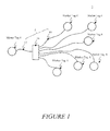
- FIG. 1 illustrates an example of a monitoring system 2 in accordance with an embodiment of the present invention.
- the system 2 includes a master tag 4 and a group of marker tags 6.
- the marker tag 6 is a tag containing a unique ID.
- the marker tag 6 is applied to an item that is to be traced.
- the master tag 4 is an entry point providing access to a group of marker tags 6, through the RF field of an RFID reader.
- the terms “monitor”, “track” and “trace” may be used interchangeably.
- “6" may represent "(individual) marker tag” or "marker tags”.
- Each marker tag 6 is physically connected to the master tag 4 via a wired connection system 8.
- the wired connection system 8 is a conductive-coupling module for coupling between the master tag 4 and the marker tags 6.
- connect (or connected) may be used interchangeably, and may indicate that two or more elements are directly or indirectly in contact with each other.
- the wired connection system 8 includes a cable 10 that is detachably connected to the marker tag 6.
- the wired connection system 8 may include a connection module 14 for dispatching signals on the marker tags 6.
- the connection module 14 may be a junction box (e.g., 14A of Figures 4 , 6 and 8 ). The junction box allows grouping all the connexions of the marker tags 6 to the single master tag 4.
- the wired connection system 8 may further include a cable 12 for connecting the master tag 4 to the connection module 14.
- the master tag 4 may be directly wired-connected to the marker tag 6 without using the connection module 14.
- the cable 10 may be a twisted pair cable or a coax cable.
- the cable 12 may be a twisted pair cable or a coax cable.
- the coax cable provides a long distance wired communication line for tags.
- the master tag 4 is operable in the RF field of the RFID reader (e.g., 50 of Figures 4 , 6 , and 8 ).
- the marker tags 6 are activated through the wired connection system 8.
- Data signals output from the RFID reader are transferred to the master tag 4, and then to the marker tags through the wired connection system 8.
- the marker tag 6 contains readable or readable/writable information (e.g., ID, information associated with an item to be tracked). The information read from the marker tag 6 is transmitted to the master tag 4 through the wired connection system 8.
- the system 2 allows for an automatic "on the fly” reading of the information stored in the marker tag 6 through the master tag 4.
- the marker tags 6 are repaired through the master tag 4.
- Information stored in the marker tag 6 is replaced through the master tag 4.
- the marker tags 6 are controlled through the single entry point, i.e., the master tag 4.
- the marker tags 6 may be used to tag items in an enclosure (e.g., a container, a box), which are not easily accessible from outside of the enclosure.
- the master tag 4 is located at a place where it is easily readable, and is used to collect information from the marker tags 6.
- the marker tag 6 and the corresponding item are immediately checked and tracked through the master tag 4.
- the marker tag 6 is detachable connected to the wired connection system 8.
- the item and its marker tag can be easily replaced with a new item and its new tag, respectively.
- marker tags 6 are shown. However, the number of the marker tags 6 is not limited to six and may vary in dependence upon the system design or requirements.
- one master tag 4 is shown. However, the number of the master tag 4 is not limited to one and may vary in dependence upon the system design or requirements. In another example, one master tag 4 may be connected to one marker tag 6 in a one to one relationship.
- the marker tag 6 of Figure 1 is described in detail.
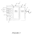
- Figure 2 illustrates an example of the marker tag 6 of Figure 1 .
- the marker tag 6 includes a tag module 20.
- the tag module 20 includes an antenna system having a primary antenna 22 and a chip 24.
- the primary antenna 22 may be a coil antenna.
- the chip 24 has a unique address and can be addressed uniquely through a tag protocol.
- the tag module 20 is accessed through the primary antenna 22.
- the marker tag 6 further includes a secondary antenna 30.
- the secondary antenna 30 may be a coil antenna.
- the secondary antenna 30 may be same or similar to the primary antenna 22.
- the secondary antenna 30 is connected to the cable 10.
- the secondary antenna 30 is located physically near the primary antenna 22, however, not electrically connected to the primary antenna 22.
- the primary antenna 22 and the secondary antenna 30 are inductively coupled, and have functionality similar to a voltage transformer.
- the primary antenna 22 and the secondary antenna 30 are positioned so that the magnetic field crossing one of the antennas will cross in the same manner the other antenna.
- the secondary antenna 30 turns on the resonant frequency same as that of the primary antenna 22. All energy/signals can be transfer from one of the antennas to the other antenna.
- the tag module 20 communicates with RFID readers (e.g., 50 of Figures 4 , 6 , and 8 ) using the cable 10.
- the tag module 20 may commutate with the RFID readers using RF signals through the secondary antenna 30, the primary antenna 22 or a combination thereof.
- tags For communications between an RFID reader and the marker tag 6, "Tag-Talks-First (TTF)" protocol or "Reader-Talks-First (RTF)” protocol may be used.
- TTF Tag-Talks-First
- RTF Reader-Talks-First
- the tag module 20 employs a standard design of RFID circuit and operates in accordance with ISO tag standards, such as ISO 15693 protocols.
- the tag module 20 is a passive RFID tag.
- the tag module 20 derives its energy based on signals received through the cable 10 or signals directly received by the marker tag 6 (e.g., the primary antenna 22, the secondary antenna 30).
- the tag module 20 may be an RFID read tag or an RFID read/write tag, which is operable by the RFID readers.
- the chip 24 includes a memory 26 and a logic section 28 for reading from the memory 26 or reading and writing to the memory 26.
- the memory 26 includes a plurality of memory blocks, each of which is selectively readable or readable and writeable. In Figure 2 , three memory blocks 26A, 26B and 26C are shown. However, the number of the memory blocks may vary in dependence upon the system design.
- the memory 26 may include one memory block.
- the memory 26 stores a unique ID that is used as the tag's unique address.
- An RFID reader uses the unique ID allocated to the marker tag 6 to identify that tag or an item to which the tag is affixed, and to select the tag.
- the memory 26 may further store data, such as time dependent information (e.g., date) and information on the item or tag (e.g., configuration).
- the memory 26 may include a Read-Only Memory (ROM), a Random Access Memory (RAM) and a Non-Volatile Programmable Memory.
- ROM Read-Only Memory
- RAM Random Access Memory
- Non-Volatile Programmable Memory may take various forms, e.g., Electrically Erasable Programmable Read Only Memory (EEPROM).
- the primary antenna 22 and the chip 24 are shown separately from each other. However, the primary antenna 22 and the chip 24 may be integrated into one circuit board and may be in physical or electrical or magnetic contact with each other.
- the memory 26 and the logic section 28 are shown separately from each other. However, the memory 26 and the logic section 28 may be integrated into one single integrated circuit.
- the secondary antenna 30 is connected to the cable 10 through a connector 32.
- the connector 32 is attached to the cable 10.
- the marker tag 6 is detachably connected to the connector 32 so that the marker tag 6 can be easily separated from the connector 32 and may be replaced with a new marker tag. In order for the replacement, an operator plugs the connector 32 to the new marker tag 6.
- the secondary antenna 30 may be directly connected to the cable 10 without using the connector 32.
- the tag module 20 and the secondary antenna 30 are in a package 34, and form a single module.
- the secondary antenna 30 may be provided separately from the tag module 20 and be located outside the package 34.
- the master tag 4 of Figure 1 is described in detail.
- the master tag 4 includes an antenna connected to the cable 12, and may have no RF tag function ( Figure 3 ).
- the master tag 4 may include a full standard RFID tag in addition to the antenna ( Figure 5 )
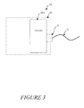
- FIG 3 illustrates an example of the master tag 4 of Figure 1 .
- the master tag 4A of Figure 3 includes an antenna 40A.
- the antenna 40A is coupled with the cable 12 through a connector 42.
- the connector 42 may be same or similar to the connector 32 of Figure 2 .
- the master tag 4A may be detachably connected to the connector 42. In another example, the master tag 4A may be directly connected to the cable 12.
- the antenna 40A may be on a Printed Circuit Board (PCB) or in a package (44).
- the antenna 40A may be a coil antenna.
- the antenna 40A may be same or similar to the secondary antenna 30 of Figure 2 .
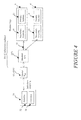
- FIG 4 illustrates an example of a coupling among an RFID reader, the master tag 4A and the marker tag 6.
- the RFID reader 50 of Figure 4 includes an antenna 52 for communicating with tags and reader circuitry 54.
- the antenna 52 may be a coil antenna.
- the RFID reader 50 may include a battery and the antenna 52 may be battery powered.
- the RFID reader 50 implements read operations on tags.
- the RFID reader 50 may implement write operations on the tags.
- the antenna 40A of the master tag 4A is inductive-coupled with the RFID reader antenna 52.
- "antenna 52" and “RFID reader antenna 52" are used interchangeably.
- the marker tags 6 communicate with the master tag 4A through a wired connection system 8A.
- the wired connection system 8A corresponds to the wired connection system 8 of Figure 1 and includes a junction box 14A.
- the junction box 14A corresponds to the connection module 14 of Figure 1 .
- the junction box 14A may be a pure connecting box, or may be made of electronic components (e.g., capacitors and inductors), to split the signal into several channels, for each marker tag 6.
- the junction box 14A is a passive device, which can be seen as a signal splitter.
- two marker tags 6 are shown. However, the number of the marker tags 6 is not limited to two and may vary in dependence upon the system design or requirements.
- one master tag 4A is shown. However, the number of the master tag 4A is not limited to one and may vary in dependence upon the system design or requirements.
- the system may include a plurality of master tags 4A, each being coupled with a different group of marker tags 6.
- the RFID reader antenna 52 creates an electro-magnetic field.
- the marker tag 6 is activated (powered up) through the wired connection system 8A (conductive-coupling).
- High Frequency (HF) signals are circulated from the master tag 4A to the secondary antenna 30 of each marker tag 6.
- Data signals from the RFID reader 50 are transmitted to the marker tag 6 through the wired connection system 8A.
- Information read from the tag module (20 of Figure 3 ) of the marker tag 6 is transmitted through the wired connection system 8A to the master tag 4A.
- the master tag 4A is coupled with the RFID antenna 52.
- the RFID reader 50 receives the information read from the marker tag 6 through the master tag 4A.
- the marker tag 6 communicates with the RFID reader 50 using the master tag 4A. However, the marker tag 6 may directly communicate with the RFID reader 50.
- the master tag 4A is connected to the marker tag 6 through the junction box 14A. However, the master tag 4A may be directly connected to the marker tag 6.
- FIG 5 illustrates another example of the master tag 4 of Figure 1 .
- the master tag 4B of Figure 5 includes a secondary antenna 40B and a tag module 60.
- the secondary antenna 40B may be same or similar to the antenna 40A of Figure 3 , and may be a coil antenna.
- the tag module 60 may be same or similar to the tag module 20 of Figure 2 .
- the tag module 60 includes an antenna system having a primary antenna 62 and a chip 64.
- the primary antenna 62 may be same or similar to the primary antenna 22 of Figure 2 , and may be a coil antenna.
- the chip 64 may be same or similar to the chip 24 of Figure 2 .
- the chip 64 has a unique address and can be addressed uniquely through a tag protocol.
- the tag module 60 is accessed through the primary antenna 62.
- the secondary antenna 40B is located physically near the primary antenna 62 to implement inductive-coupling, however, not electrically connected to the primary antenna 62.
- the primary antenna 62 and the secondary antenna 40B have functionality similar to a voltage transformer.
- the primary antenna 62 and the secondary antenna 40B are positioned so that the magnetic field crossing one of the antennas will cross in the same manner the other antenna.
- the secondary antenna 40B turns on the resonant frequency same as that of the primary antenna 62. All energy/signals can be transfer from one of the antennas to the other antenna.
- the tag module 60 may be an RFID read tag or an RFID read/write tag, which is operable by RFID readers (e.g., 50 of Figures 4 , 6 , and 8 ).
- the tag module 60 may be a passive tag or an active tag that includes a battery.
- the chip 64 includes a memory 66 and a logic section 68 for reading from the memory 66 or reading and writing to the memory 66.
- the memory 66 includes a plurality of memory blocks, each of which is selectively readable or readable and writeable. In Figure 5 , three memory blocks 66A, 66B and 66C are shown. However, the number of the memory blocks may vary in dependence upon the system design.
- the memory 66 may include one memory block.
- the memory 66 stores a unique ID that is used as the tag's unique address.
- An RFID reader uses the unique ID allocated to the master tag 4B to identify that tag or an item to which the tag is affixed, and to select the tag.
- the memory 66 may further store data, such as time dependent information (e.g., date) and information on the item or tag (e.g., configuration).
- the tag module 60 may communicate with RFID readers directly through the primary antenna 62 or through the secondary antenna 40B.
- RFID readers For communications between an RFID reader and the tag module 60, "Tag-Talks-First (TTF)” protocol or "Reader-Talks-First (RTF)” protocol may be used.
- TTF Tag-Talks-First
- RTF Reader-Talks-First
- the tag module 60 employs a standard design of RFID circuit and operates in accordance with ISO tag standards, such as ISO 15693 protocols.
- the primary antenna 62 and the chip 64 are shown separately from each other. However, the primary antenna 62 and the chip 64 may be integrated into one circuit board and may be in physical or electrical or magnetic contact with each other.
- the memory 66 and the logic section 68 are shown separately from each other. However, the memory 66 and the logic section 68 may be integrated into one single integrated circuit.
- the tag module 60 and the secondary antenna 40B may be in a package 70, and form a single module.
- the secondary antenna 40B may be provided separately from the tag module 60 and be located outside the package 70.
- Figure 6 illustrates an example of a coupling among the RFID reader, the master tag 4B and the marker tag 6.
- the primary antenna 62 and the secondary antenna 40B may form a single module in a package (e.g., 70 of Figure 5 ) or may be different modules.
- the RFID reader antenna 52, the primary antenna 62 of the master tag 4B and the secondary antenna 40B of the master tag 4B are in close inductive-coupling so that any energy or data signals transmitted from one antenna is received on the other antennas.
- the ID of the master tag 4B represents a group of the marker tags 6.
- the marker tags 6 communicate with the master tag 4B through the wired connection system 8A.
- the secondary antenna 40B of the master tag 4B is conductively coupled with the secondary antenna 30 of the marker tag 6.
- two marker tags 6 are shown. However, the number of the marker tags 6 is not limited to two and may vary in dependence upon the system design or requirements.
- one master tag 4B is shown. However, the number of the master tag 4B is not limited to one and may vary in dependence upon the system design or requirements.
- the system may include a plurality of master tags 4B, and the ID of each master tag 4B may represent a different group of marker tags 6.
- both of the primary antenna 62 and the secondary antenna 40B receive the RF signals, because of the proximity.
- the RFID reader 50 acts as an emitter and both of the antennas 40B and 62 in the master tag 4B act as receivers or dual secondary antennas. It is similar to a transformer having three coil-antennas.
- any coding read from the marker tag 6 is transmitted through the wired connection system 8A to the secondary antenna 40B of the master tag 4B.
- the secondary antenna 40B is coupled to the primary antenna 62 and the RFID reader antenna 52.
- the RFID reader 50 receives information read from the marker tag 6.
- the RFID reader 50 may receive information read from the tag module (60) of the master tag 4B.
- the RFID reader 50 communicates with both of the primary antenna 62 and the secondary antenna 40B in the master tag 4B at the same time. After that, the coupling among these antennas depends on a geometric balance, such as the sizes of their coils and distances among the coils.
- the RFID reader 50 may directly or indirectly communicate with the secondary antenna 40B, the primary antenna 62 or a combination thereof.
- the primary 62 may be a large size coil.
- the large size coil (primary antenna) 62 grasps the energy generated by the RFID reader 50 and then transfers it to the secondary antenna 40B.
- the distance between the RFID reader antenna 52 and the primary antenna 62 or the distance between the RFID reader antenna 52 and the secondary antenna 40B may be larger than the distance between the primary antenna 62 and the secondary antenna 40, due to ergonomics/practical reasons.
- the marker tag 6 communicates with the RFID reader 50 using the master tag 4B through the wired cable (conductive-coupling) 8A. However, the marker tag 6 may directly communicate with the RFID reader 50.
- the master tag 4B is connected to the marker tag 6 through the junction box 14A. However, the master tag 4B may be directly connected to the marker tag 6.
- the system 2 uses a simultaneous multiple access function, called anti-collision algorithm for operating on a plurality of tags.
- the tag anti-collision function may be implemented in the tag/reader protocol, allowing all tags to be addressed in a one by one manner, with a time slot system.
- the system 2 may employ anti-collision mechanism in accordance with the standard ISO 15693-3.
- the RFID reader (e.g., 50 of Figures 4 , 6 , and 8 ) has an RFID tag protocol that defines how to address a particular tag, how to read the ID, or how to read a particular memory block of that particular tag. All that protocol is part of standard tag protocol. All of the tags are activated, however, selective read/write to specific addresses can be achieved.
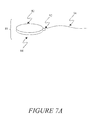
- Figures 7A-7C illustrate an example of the structure of the marker tag 6 of Figure 1 .
- the tag of Figures 7A-7C is made of a multilayer PCB 80.
- the PCB 80 has two layers 82 and 84.
- the chip 86 corresponds to the chip 24 of Figure 2 .
- the primary coil 88 corresponds to the primary antenna 22 of Figure 2 .
- the secondary coil 90 corresponds to the secondary antenna 30 of Figure 2 .
- the primary coil 88 and the secondary coil 90 are inductively coupled.
- the secondary coil 90 is connected to a cable through the wire connector 92.
- the connector 92 corresponds to the connector 32 of Figure 2 .
- the connector 92 may be a small Surface Mount Device (SMD) type connector, to connect the layer 84 on the PCB to a double wire (e.g., cable 10 of Figure 1 ). There are no connections between the first layer 82 and the second layer 84.
- SMD Surface Mount Device
- the representation of the primary coil 88 and the secondary coil 90 is schematic only, and the actual configuration of the primary coil 88 and the secondary coil 90 may take on a variety of configurations.
- the interface to the tag is implemented at the connector level, and the tag and its associated secondary antenna is designed on the same unitary component.
- the marker tag 6 is activated as soon as its connector 92 is linked to the master tag and the HF signal propagates into the wire cable (conductive coupling) through the connector 92.
- the master tag 4B of Figure 5 may have the structure that is same or similar to that of Figures 7A-7C .
- the primary coil 88 corresponds to the primary antenna 62 of Figure 5
- the chip 86 corresponds to the chip 64 of Figure 5
- the secondary coil 90 corresponds to the secondary antenna 40B of Figure 5
- the connector 92 corresponds to the connector 42 of Figure 5 .
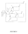
- Figure 8 illustrates an exemplary scenario applied to the system 2 of Figure 1 .
- the marker tags 6 are placed on items 100 that are to be tracked.
- the items 100 may be, but not limited to, electronic boards, an assembled unit forming one component, or mechanical parts.
- the items 100 are in an enclosure 102.
- the enclosure 102 may be, but not limited to, a sealed electric box, a sealed metal box, or an electrical cabinet, so that RF signals may not pass through the enclosure 102.
- the marker tags 6 are connected to the master tag 4 through the wired connection system 8A.
- the master tag 4 may be the master tag 4A of Figure 3 or the master tag 4B of Figure 5 .
- the junction box 14A is located in the enclosure 102. However, the junction box 14A may be located outside the enclosure 102.
- the master tag 4 is located at a place where it is easily readable by the RFID reader 50.
- the RFID reader 50 may be a hand-held RFID reader or a fix reading station having RFID reader functions.
- the RFID reader 50 may communicate with an external computer-based device and use a wired or some other wireless radio protocols to communicate with that computer-based device.
- the RFID reader 50 may include a user interface, such as a display, input devices and sound devices.
- the master tag 4 is mounted on the external side of the enclosure 102. In an other example, the master tag 4 may be outside the enclosure 102 and be separated from the enclosure 102. The cable 12 connected to the master tag 4 goes inside the enclosure 102.
- the RFID reader 50 sends the RF energy through its antenna 52 to the master tag 4.
- the master tag 4 transmits the energy to the marker tags 6 through the wired connection system 8A.
- the RFID reader 50 communicates with the marker tags 6 through the master tag 4, and can address a particular marker tag or a particular memory block of that particular marker according to the tag communication protocol.
- the IDs of all marker tags are scanned and reported under the control of the RFID reader 50.
- a particular field stored in the memory e.g., a memory block 26A, 26B, or 26C of Figure 2
- a particular memory field for a particular tag is scanned and reported under the control of the RFID reader 50.
- Identification information and particular information associated with the marker tag 6 and the item 100 is collected at the master tag 4. Thus, the information in the marker tag 6 is readable without opening the enclosure 102.
- the enclosure 102 may be a shield, electrical cabinet in a train or a vehicle (hereinafter referred to as cabinet 102).
- the master tag 4 may be placed underneath the train or vehicle or on the side or top of the train or vehicle.
- all IDs of the marker tags 6 are read through the master tag 4.
- the operator of the RFID reader 50 may update a particular field of a marker tag through the master tag 4.
- an operator When replacing the item 100, an operator removes the connector (e.g., 32 of Figure 2 , 92 of Figures 7A and 7C ) from the marker tag 6, and replaces the item 100 with a new item that is fitted with its proper new marker tag. The operator reconnects the connector to the new marker tag. When the system tracks the new item, information on the new marker tag is read.
- the connector e.g., 32 of Figure 2 , 92 of Figures 7A and 7C
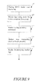
- FIG 9 illustrates an example of a method of operating the system 2 of Figure 1 .
- an RFID reader e.g., 50 of Figures 4 , 6 and 8
- the RFID reader sends the RF energy to the master tag 4, which transmits this energy to the marker tags 6 through the wired connection system 8.
- the marker tags 6 connected to the master tag 4 are powered up and are ready to communicate with the RFID reader (step 112).
- the RFID reader issues a tag inventory command (step 114).
- Each marker tag 6 makes a response using its unique ID (step 116). If a collision occurs, the RFID reader detects the collision. The collision is resolved by the anti-collision mechanism.
- the anti-collision process is implemented until there are no more collisions and the RFID reader identifies all marker tags 6 connected to the master tag 4. Once the RFID reader has inventories all marker tags connected to the master tag 4 (step 118), the RFID reader can access an individual marker tag through the master tag 4 for reading or reading and writing operations.
- the master tag 4 (e.g., 4B of Figure 5 ) may respond to the RFID reader in accordance with the anti-collision mechanism, using its unique ID.
- the marker tags 6 are operated through the master tag 4. However, in another example, the marker tags 6 may directly respond to the RFID reader. In this example, the marker tag 6 is placed within the RF field of the RFID reader. The marker tag 6 is powered up by signals directly received from the RFID reader. The RFID reader directly obtains the ID of the marker tag 6.
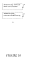
- FIG 10 illustrates an example of a method for read mode operation for the system 2 of Figure 1 .
- the RFID reader e.g., 50 of Figures 4 , 6 and 8
- the RFID reader has the IDs of the marker tags 6.
- the master tag 4 is within the RF field of the RFID reader.
- the RFID reader sends an addressed mode read command to a particular marker tag 6, and a particular memory block in the particular marker tag 6 (step 120).
- the unique ID allocated to each marker tag is used to access that particular marker tag.
- the RFID reader receives through the master tag 4 information read from the particular memory block in the particular marker tag 6 (step 122).
- the addressed mode read command is, for example, based on ISO 15693-3 tag protocol.
- the RFID reader may read information from the master tag 4 (e.g., 4B of Figure 5 ), using the tag's unique ID.
- the marker tags 6 are operated through the master tag 4.
- the RFID reader may directly read information from the marker tag 6.
- the marker tag 6 is placed within the RF field of the RFID reader.
- FIG 11 illustrates an example of a method for write mode operation for the system 2 of Figure 1 .
- the RFID reader e.g., 50 of Figures 4 , 6 and 8
- the RFID reader has the IDs of the marker tags 6.
- the master tag 4 is within the RF field of the RFID reader.
- the RFID reader sends an addressed mode write command to a particular marker tag, and a particular memory block in the particular marker tag 6 (step 124).
- the unique ID allocated to each marker tag is used to access a particular marker tag.
- the RFID reader sends an addressed mode read command to check that the reading has been completed (step 126), similar to the step 120 of Figure 10 .
- the RFID reader receives through the master tag 4 information read from the particular memory block in the particular marker tag 6 (step 128), similar to the step 122 of Figure 10 .
- the addressed mode read command and the addressed mode write command are, for example, based on ISO 15693-3 tag protocol.
- the RFID reader may implement the write and read operation on the master tag 4 (e.g., 4B of Figure 5 ), using the tag's unique ID.
- the marker tags 6 are operated through the master tag 4.
- the RFID reader may directly write information on the marker tag 6.
- the marker tag 6 is placed within the RF field of the RFID reader.
- FIG 12 illustrates an example of a monitoring system 150 in accordance with another embodiment of the present invention.
- the system 150 includes a secondary antenna 152 for one or more than one marker tag 154, and a wired connection system 160 for connecting the secondary antenna 152 and the master tag 4.
- the secondary antenna 152 may be a coil antenna.
- the marker tag 154 is applied to an item that is to be traced. In the description, "154" may represent "(individual) marker tag" or "(a group of) marker tags”.
- the marker tag 154 may be same or similar to the tag module 20 of Figure 2 .
- the marker tag 154 contains a primary antenna (e.g., 156 of Figure 13 ) and RF tag functions.
- the marker tag 154 contains readable information or readable/writeable information in its memory block(s), e.g., a unique ID.
- the marker tag 154 does not include a secondary antenna.
- the secondary antenna 152 may be same or similar to the secondary antenna 30 of Figure 2 .
- the secondary antenna 152 and the primary antenna (e.g., 156 of Figure 13 ) of each marker tag 154 are coupled by inductive-coupling.
- the wired connection system 160 includes a cable 162 that is connected to the secondary antenna 152.
- the cable 162 may be detachably connected to the secondary antenna 152.
- the wired connection system 160 may include a connection module 164 for connecting the cable 162 to the master tag 4.
- the connection module 164 may be same or similar to the connection module 14 of Figure 1 .
- the connection module 164 may be a junction box (e.g., 14A of Figures 4 , 6 and 8 ).
- the wired connection system 160 may further include a cable 166 for connecting the master tag 4 to the cable 162.
- the master tag 4 may be directly wired-connected to the secondary antenna 152 without using the connection module 164.
- the cable 162 may be a twisted pair cable or a coax cable.
- the cable 166 may be a twisted pair cable or a coax cable.
- the wired connection system 160 may be same or similar to the wired connection system 8 of Figure 1 or 8A of Figures 4 , 6
- one master tag 4 is shown. However, the number of the master tag 4 is not limited to one and may vary in dependence upon the system design or requirements.
- one secondary antenna 152 is shown. However, the number of the secondary antenna 152 is not limited to one and may vary in dependence upon the system design or requirements.
- one master tag 4 may be connected to a plurality of secondary antennas 152.
- three marker tags 154 are shown. However, these marker tags 154 are representative only.
- one cable 162 is shown. However, the number of the cables 162 is not limited to one and depends on the number of the secondary antennas 152. A plurality of cables 162 may be connected to the master tag 4 through the connection module 164.
- the system 150 may include a plurality of secondary antennas 152 and a plurality of master tags 4, and each master tag 4 may represent one secondary antenna 152 or a group of secondary antennas 152.
- Figure 13 illustrates an exemplary scenario applied to the system 150 of Figure 12 .
- the marker tag 154 is allocated to an item 100 that is to be traced.
- the marker tag 154 is, for example, placed on a frame of the item 100.
- the secondary antenna 152 is located at a particular position/location.
- the item 100 is moved into a certain area associated with the particular position of the secondary antenna 152 when it is to be tracked.
- a link between the secondary antenna 152 and the marker tag 154 is established.
- the marker tag 154 is seen by the secondary antenna 152 (inductive-coupling).
- the marker tag 154 is, for example, a passive tag.
- the marker tag 154 is energized by signals that are received through the wired connection system 160 or the secondary antenna 152, or received directly at its antenna 156.
- the marker tag 154 is an RFID read tag or an RFID read-write tag.
- An RFID reader (e.g., 50, Figures 4 , 6 and 8 ) may implement the operation processes on the marker tag 154, similar to those of Figures 9-11 .
- the RFID reader accesses the marker tag 154 through the master tag 4.
- the RFID reader may directly operate on the marker tags 154.
- a memory block in the marker tag 154 may be read or read/written by the RFID reader using tag protocols.
- a particular memory block in a particular marker tag 154 may be read or read/written by the RFID reader using tag protocols (e.g., ISO 15693-3).
- the marker tag i.e., 6 of Figure 2 , 154 of Figure 13
- communicates with RFID readers using the secondary antenna i.e., 30 of Figure 2 , 152 of Figure 13
- the secondary antenna is directly connected to the wired connection system (i.e., 8 of Figure 2 , 160 of Figure 13 ).
- the tag antenna of the marker tag is directly connected to the wired connection system as shown in Figure 14 .
- FIG 14 illustrates an example of a monitoring system 180 in accordance with a further embodiment of the present invention.
- the system 180 includes a group of marker tags 182.
- the marker tag 182 includes a tag module containing a unique ID.
- the marker tag 182 may be an RFID read tag or an RFID read/write tag.
- the marker tag 182 may employ a standard design of RFID circuit and operate in accordance with ISO tag standards (e.g., ISO 15693 protocols).
- ISO tag standards e.g., ISO 15693 protocols.
- the marker tag 182 is applied to an item that is to be traced.
- Each marker tag 182 has a tag antenna 184 and a chip 186.
- the tag antenna 184 and the chip 186 form a single tag module.
- the marker tag 182 is accessed through the tag antenna 184.
- the tag antenna 184 may be a coil antenna.
- the chip 186 has a unique address and can be addressed uniquely through a tag protocol (e.g., ISO 15693 protocols).
- the tag antenna 184 is physically connected to the cable 10.
- the tag antenna 184 may be detachably connected to the cable 10 via a connector similar to the connector 32 of Figure 3 .
- the marker tags 182 communicate with RFID readers (e.g., 50 of Figures 4 , 6 , and 8 ) via the wired connection system 8.
- the marker tags 182 are readable and writable via the master tag 4.
- the marker tags 182 are controlled through the master tag 4.
- the tag antenna 184 and the chip 186 are shown separately. However, the tag antenna 184 and the chip 186 may be integrated into one circuit board and may be in physical or electrical or magnetic contact with each other.
- the marker tag 182 may be same or similar to the tag module 20 of Figure 2 .
- the tag antenna 184 may be same or similar to the primary antenna 22 of Figure 2 .
- the chip 186 may be same or similar to the chip 24 of Figure 2 , and includes a logic circuit and a memory having one or more than one memory block.
- a particular memory block in a particular marker tag 154 may be read or read/written by the RFID reader using tag protocols (e.g., ISO15693-3).
- the system 180 of Figure 14 may be operated in accordance with the steps of Figures 9-11 .
- the marker tag 182 is a passive RFID tag.
- the marker tag 182 derives its energy based on signals received through the cable 10 or signals directly received by the tag antenna 184.
- three marker tags 182 are shown. However, the number of the marker tags 182 is not limited to three and may vary in dependence upon the system design or requirements.
- one master tag 4 is shown. However, the number of the master tag 4 is not limited to one and may vary in dependence upon the system design or requirements. In a further example, one master tag 4 may be connected to one marker tag 182 in a one to one relationship.
- the master tag 4 in the above embodiments may be same or similar to the marker tag 182.
- the tag antenna of the master tag 4 may be directly connected to the wired connection system (i.e., 8 of Figures 1 and 14 , 160 of Figure 12 ).
- the wired connection system 8 of Figures 1 and 14 may be same or similar to the wired connection system 160 of Figure 12 .
- the system 180 may include the wired connection system 160 of Figure 12 .
Landscapes
- Engineering & Computer Science (AREA)
- Physics & Mathematics (AREA)
- General Physics & Mathematics (AREA)
- Theoretical Computer Science (AREA)
- Health & Medical Sciences (AREA)
- Computer Vision & Pattern Recognition (AREA)
- Artificial Intelligence (AREA)
- Toxicology (AREA)
- Electromagnetism (AREA)
- Computer Hardware Design (AREA)
- Microelectronics & Electronic Packaging (AREA)
- Computer Networks & Wireless Communication (AREA)
- General Health & Medical Sciences (AREA)
- Near-Field Transmission Systems (AREA)
- Burglar Alarm Systems (AREA)
Description
- The present invention relates to Radio Frequency Identification (RFID) technology, and more specifically to RFID based monitoring system and method.
- The process of tracking items requires that each item have its own readable information. Conventionally, each item is marked locally with a visible serial number, which is printed on a label, or is used with a bar code having a machine-readable serial number. Such serial numbers may be correctly read when the items are located so that the serial numbers on the items can be visually observed or be scanned by a bar code scanner. However, manual reading may introduce errors. Further, the items may be in a shield boundary (e.g., cabinet) and are not easily accessible from outside. In this case, it is necessary to open the boundary to read the serial number on each item.
- Radio frequency identification (RFID) tags function as contactless markers. Each RFID tag has its own unique identification or identifier (ID). The IDs on the RFID tags are read by an RFID reader using RF signals, and can be used for inventory purpose. Items having the RFID tags can be tracked using the IDs of the tags. The RFID tags can be either active or passive RFID tags. An active RFID tag is used in a variaty of applications since the active RFID tag has its own internal power source. However, the size and cost for the active RFID tag is high. In addition, when tracking items in the shield boundary, there is no way to know how many active RFID tags will answer to the RFID reader. Moreover, there may be a confusion between the items supposed to be read and the IDs obtained. The operator of the RFID reader may not know the items in the boundary. The operator may not know where the items are in the boundary.
- Therefore, there exists a need for a method and system to improve the access to the item's ID. There is also a need for a method and system to improve the time to scan/read the ID among multiple IDs for inventory purpose.
DE10113719 A1 provides a system for monitoring components in a car. The system includes a receiver, and a transponder for transmitting data from the components to the receiver.EP1672560 A1 provides an inductive identification system having a transponder, a 'transmitter and receiver' device, and a coupling unit for communication between the transponder and the 'transmitter and receiver' device.US2003/122655 A1 provides a short range communication system having an interrogator, transponders, and coupling ports for communication between the interrogator and the transponders. - It is an object of the invention to provide a method and system that obviates or mitigates at least one of the disadvantages/limitations of existing systems. In accordance with a first aspect of the invention, an apparatus having the features of appended
claim 1 is provided. In accordance with a second aspect of the invention, an apparatus having the features of appended claim 19 is provided. In accordance with a third aspect of the invention, a method having the steps of appendedclaim 20 is provided. The dependent claims provide details of features and steps of embodiments. - In accordance with an aspect of the present invention, there is provided a system for monitoring one or more than one item. The system includes a master tag operable in an RF field of an RFID reader, and a connection system for accessing one or more than one marker tag allocated to the one or more than one item, respectively, through conductive coupling. Each of the one or more than one marker tag includes a unique ID and is operable by the RFID reader. The connection system is conductively coupled with the master tag and includes a cable for coupling each of the one or more than one marker tags to the master tag, so that the one or more than one marker tag is readable through the conductive coupling by the RFID reader.
- In accordance with another aspect of the present invention, there is provided a system for monitoring an item. The system includes a tag module having a unique ID and a first antenna. The tag module is operable by an RFID reader. The system includes a second antenna for accessing the tag module. The second antenna is conductively coupled, through conductive coupling with a master tag operable in an RF field of the RFID reader. The second antenna is inductively coupled with the first antenna, so that the tag module is readable through a combination of conductive and inductive coupling by the RFID reader.
- In accordance with a further aspect of the present invention, there is provided a method of monitoring one or more than one item. The method includes allocating one or more than one marker tag to the one or more than one item, respectively. Each of the one or more than one marker tag includes a unique ID and is operable by an RFID reader. The method includes accessing the one or more than one marker tag through conductive coupling. The step of accessing includes conductively coupling a master tag operable by the RFID with a connection system for accessing the one or more than one marker tag via a cable, and reading the one or more than one marker tag with the RFID reader through the master tag.
- This summary of the invention does not necessarily describe all features of the invention.
- These and other features of the invention will become more apparent from the following description in which reference is made to the appended drawings wherein:
-
Figure 1 is a schematic diagram illustrating an example of a monitoring system in accordance with an embodiment of the present invention; -
Figure 2 is a schematic diagram illustrating an example of a marker tag ofFigure 1 ; -
Figure 3 is a schematic diagram illustrating an example of a master tag ofFigure 1 ; -
Figure 4 is a schematic diagram illustrating an example of a coupling among an RFID reader, the master tag and the marker tag; -
Figure 5 is a schematic diagram illustrating another example of the master tag ofFigure 1 ; -
Figure 6 is a schematic diagram illustrating another example of the coupling among the RFID reader, the master tag and the marker tag; -
Figure 7A is a perspective view illustrating an example of the layered structure of the marker tag; -
Figure 7B is a schematic diagram illustrating an example of one layer ofFigure 7A ; -
Figure 7C is a schematic diagram illustrating an example of another layer ofFigure 7A ; -
Figure 8 is a schematic diagram illustrating an exemplary scenario applied to the system ofFigure 1 ; -
Figure 9 is a flowchart illustrating an example of a method of operating the monitoring system ofFigure 1 ; -
Figure 10 is a flowchart illustrating an example of a method for read mode operation for the monitoring system ofFigure 1 ; -
Figure 11 is a flowchart illustrating an example of a method for read mode operation for the monitoring system ofFigure 1 ; -
Figure 12 is a schematic diagram illustrating an example of a monitoring system in accordance with another embodiment of the present invention; -
Figure 13 is a schematic diagram illustrating an exemplary scenario applied to the system ofFigure 12 ; and -
Figure 14 is a schematic diagram illustrating an example of a monitoring system in accordance with another embodiment of the present invention. -
Figure 1 illustrates an example of amonitoring system 2 in accordance with an embodiment of the present invention. Thesystem 2 includes amaster tag 4 and a group of marker tags 6. Themarker tag 6 is a tag containing a unique ID. Themarker tag 6 is applied to an item that is to be traced. Themaster tag 4 is an entry point providing access to a group ofmarker tags 6, through the RF field of an RFID reader. In the description, the terms "monitor", "track" and "trace" may be used interchangeably. In the description, "6" may represent "(individual) marker tag" or "marker tags". - Each
marker tag 6 is physically connected to themaster tag 4 via awired connection system 8. Thewired connection system 8 is a conductive-coupling module for coupling between themaster tag 4 and the marker tags 6. In the description, the terms "connect (or connected)", "couple (or coupled) " and "link (linked)" may be used interchangeably, and may indicate that two or more elements are directly or indirectly in contact with each other. - The
wired connection system 8 includes acable 10 that is detachably connected to themarker tag 6. Thewired connection system 8 may include aconnection module 14 for dispatching signals on the marker tags 6. Theconnection module 14 may be a junction box (e.g., 14A ofFigures 4 ,6 and8 ). The junction box allows grouping all the connexions of the marker tags 6 to thesingle master tag 4. - The
wired connection system 8 may further include acable 12 for connecting themaster tag 4 to theconnection module 14. However, in another example, themaster tag 4 may be directly wired-connected to themarker tag 6 without using theconnection module 14. - The
cable 10 may be a twisted pair cable or a coax cable. Thecable 12 may be a twisted pair cable or a coax cable. The coax cable provides a long distance wired communication line for tags. - The
master tag 4 is operable in the RF field of the RFID reader (e.g., 50 ofFigures 4 ,6 , and8 ). When themaster tag 4 is within the RF field of the RFID reader, the marker tags 6 are activated through thewired connection system 8. Data signals output from the RFID reader are transferred to themaster tag 4, and then to the marker tags through thewired connection system 8. Themarker tag 6 contains readable or readable/writable information (e.g., ID, information associated with an item to be tracked). The information read from themarker tag 6 is transmitted to themaster tag 4 through thewired connection system 8. - The
system 2 allows for an automatic "on the fly" reading of the information stored in themarker tag 6 through themaster tag 4. In addition, the marker tags 6 are repaired through themaster tag 4. Information stored in themarker tag 6 is replaced through themaster tag 4. The marker tags 6 are controlled through the single entry point, i.e., themaster tag 4. - For example, the marker tags 6 may be used to tag items in an enclosure (e.g., a container, a box), which are not easily accessible from outside of the enclosure. In this case, the
master tag 4 is located at a place where it is easily readable, and is used to collect information from the marker tags 6. Themarker tag 6 and the corresponding item are immediately checked and tracked through themaster tag 4. Themarker tag 6 is detachable connected to thewired connection system 8. Thus, the item and its marker tag can be easily replaced with a new item and its new tag, respectively. - In
Figure 1 , sixmarker tags 6 are shown. However, the number of the marker tags 6 is not limited to six and may vary in dependence upon the system design or requirements. InFigure 1 , onemaster tag 4 is shown. However, the number of themaster tag 4 is not limited to one and may vary in dependence upon the system design or requirements. In another example, onemaster tag 4 may be connected to onemarker tag 6 in a one to one relationship. - The
marker tag 6 ofFigure 1 is described in detail.Figure 2 illustrates an example of themarker tag 6 ofFigure 1 . Referring toFigure 2 , themarker tag 6 includes atag module 20. Thetag module 20 includes an antenna system having aprimary antenna 22 and achip 24. Theprimary antenna 22 may be a coil antenna. Thechip 24 has a unique address and can be addressed uniquely through a tag protocol. Thetag module 20 is accessed through theprimary antenna 22. - The
marker tag 6 further includes asecondary antenna 30. Thesecondary antenna 30 may be a coil antenna. Thesecondary antenna 30 may be same or similar to theprimary antenna 22. Thesecondary antenna 30 is connected to thecable 10. Thesecondary antenna 30 is located physically near theprimary antenna 22, however, not electrically connected to theprimary antenna 22. - The
primary antenna 22 and thesecondary antenna 30 are inductively coupled, and have functionality similar to a voltage transformer. Theprimary antenna 22 and thesecondary antenna 30 are positioned so that the magnetic field crossing one of the antennas will cross in the same manner the other antenna. Thesecondary antenna 30 turns on the resonant frequency same as that of theprimary antenna 22. All energy/signals can be transfer from one of the antennas to the other antenna. - The
tag module 20 communicates with RFID readers (e.g., 50 ofFigures 4 ,6 , and8 ) using thecable 10. Thetag module 20 may commutate with the RFID readers using RF signals through thesecondary antenna 30, theprimary antenna 22 or a combination thereof. For communications between an RFID reader and themarker tag 6, "Tag-Talks-First (TTF)" protocol or "Reader-Talks-First (RTF)" protocol may be used. Thetag module 20 employs a standard design of RFID circuit and operates in accordance with ISO tag standards, such as ISO 15693 protocols. - The
tag module 20 is a passive RFID tag. Thetag module 20 derives its energy based on signals received through thecable 10 or signals directly received by the marker tag 6 (e.g., theprimary antenna 22, the secondary antenna 30). - The
tag module 20 may be an RFID read tag or an RFID read/write tag, which is operable by the RFID readers. Thechip 24 includes amemory 26 and alogic section 28 for reading from thememory 26 or reading and writing to thememory 26. Thememory 26 includes a plurality of memory blocks, each of which is selectively readable or readable and writeable. InFigure 2 , threememory blocks memory 26 may include one memory block. Thememory 26 stores a unique ID that is used as the tag's unique address. An RFID reader uses the unique ID allocated to themarker tag 6 to identify that tag or an item to which the tag is affixed, and to select the tag. Thememory 26 may further store data, such as time dependent information (e.g., date) and information on the item or tag (e.g., configuration). - The
memory 26 may include a Read-Only Memory (ROM), a Random Access Memory (RAM) and a Non-Volatile Programmable Memory. The Non-Volatile Programmable Memory may take various forms, e.g., Electrically Erasable Programmable Read Only Memory (EEPROM). - In
Figure 2 , theprimary antenna 22 and thechip 24 are shown separately from each other. However, theprimary antenna 22 and thechip 24 may be integrated into one circuit board and may be in physical or electrical or magnetic contact with each other. InFigure 2 , thememory 26 and thelogic section 28 are shown separately from each other. However, thememory 26 and thelogic section 28 may be integrated into one single integrated circuit. - The
secondary antenna 30 is connected to thecable 10 through aconnector 32. Theconnector 32 is attached to thecable 10. Themarker tag 6 is detachably connected to theconnector 32 so that themarker tag 6 can be easily separated from theconnector 32 and may be replaced with a new marker tag. In order for the replacement, an operator plugs theconnector 32 to thenew marker tag 6. In another example, thesecondary antenna 30 may be directly connected to thecable 10 without using theconnector 32. - The
tag module 20 and thesecondary antenna 30 are in apackage 34, and form a single module. However, in another example, thesecondary antenna 30 may be provided separately from thetag module 20 and be located outside thepackage 34. - The
master tag 4 ofFigure 1 is described in detail. Themaster tag 4 includes an antenna connected to thecable 12, and may have no RF tag function (Figure 3 ). Themaster tag 4 may include a full standard RFID tag in addition to the antenna (Figure 5 ) -
Figure 3 illustrates an example of themaster tag 4 ofFigure 1 . Themaster tag 4A ofFigure 3 includes anantenna 40A. Theantenna 40A is coupled with thecable 12 through aconnector 42. Theconnector 42 may be same or similar to theconnector 32 ofFigure 2 . Themaster tag 4A may be detachably connected to theconnector 42. In another example, themaster tag 4A may be directly connected to thecable 12. Theantenna 40A may be on a Printed Circuit Board (PCB) or in a package (44). Theantenna 40A may be a coil antenna. Theantenna 40A may be same or similar to thesecondary antenna 30 ofFigure 2 . -
Figure 4 illustrates an example of a coupling among an RFID reader, themaster tag 4A and themarker tag 6. TheRFID reader 50 ofFigure 4 includes anantenna 52 for communicating with tags andreader circuitry 54. Theantenna 52 may be a coil antenna. TheRFID reader 50 may include a battery and theantenna 52 may be battery powered. TheRFID reader 50 implements read operations on tags. TheRFID reader 50 may implement write operations on the tags. Theantenna 40A of themaster tag 4A is inductive-coupled with theRFID reader antenna 52. In the description, "antenna 52" and "RFID reader antenna 52" are used interchangeably. - The marker tags 6 communicate with the
master tag 4A through awired connection system 8A. Thewired connection system 8A corresponds to thewired connection system 8 ofFigure 1 and includes ajunction box 14A. Thejunction box 14A corresponds to theconnection module 14 ofFigure 1 . Thejunction box 14A may be a pure connecting box, or may be made of electronic components (e.g., capacitors and inductors), to split the signal into several channels, for eachmarker tag 6. Thejunction box 14A is a passive device, which can be seen as a signal splitter. - In
Figure 4 , twomarker tags 6 are shown. However, the number of the marker tags 6 is not limited to two and may vary in dependence upon the system design or requirements. InFigure 4 , onemaster tag 4A is shown. However, the number of themaster tag 4A is not limited to one and may vary in dependence upon the system design or requirements. The system may include a plurality ofmaster tags 4A, each being coupled with a different group of marker tags 6. - The
RFID reader antenna 52 creates an electro-magnetic field. When themaster tag 4A is located within the electro-magnetic field, themarker tag 6 is activated (powered up) through thewired connection system 8A (conductive-coupling). Based on the outputs from theRFID reader 50, High Frequency (HF) signals are circulated from themaster tag 4A to thesecondary antenna 30 of eachmarker tag 6. Data signals from theRFID reader 50 are transmitted to themarker tag 6 through thewired connection system 8A. Information read from the tag module (20 ofFigure 3 ) of themarker tag 6 is transmitted through thewired connection system 8A to themaster tag 4A. Themaster tag 4A is coupled with theRFID antenna 52. Thus, theRFID reader 50 receives the information read from themarker tag 6 through themaster tag 4A. - In
Figure 4 , themarker tag 6 communicates with theRFID reader 50 using themaster tag 4A. However, themarker tag 6 may directly communicate with theRFID reader 50. InFigure 4 , themaster tag 4A is connected to themarker tag 6 through thejunction box 14A. However, themaster tag 4A may be directly connected to themarker tag 6. -
Figure 5 illustrates another example of themaster tag 4 ofFigure 1 . Themaster tag 4B ofFigure 5 includes asecondary antenna 40B and atag module 60. Thesecondary antenna 40B may be same or similar to theantenna 40A ofFigure 3 , and may be a coil antenna. Thetag module 60 may be same or similar to thetag module 20 ofFigure 2 . Thetag module 60 includes an antenna system having aprimary antenna 62 and achip 64. Theprimary antenna 62 may be same or similar to theprimary antenna 22 ofFigure 2 , and may be a coil antenna. Thechip 64 may be same or similar to thechip 24 ofFigure 2 . Thechip 64 has a unique address and can be addressed uniquely through a tag protocol. Thetag module 60 is accessed through theprimary antenna 62. - The
secondary antenna 40B is located physically near theprimary antenna 62 to implement inductive-coupling, however, not electrically connected to theprimary antenna 62. Theprimary antenna 62 and thesecondary antenna 40B have functionality similar to a voltage transformer. Theprimary antenna 62 and thesecondary antenna 40B are positioned so that the magnetic field crossing one of the antennas will cross in the same manner the other antenna. Thesecondary antenna 40B turns on the resonant frequency same as that of theprimary antenna 62. All energy/signals can be transfer from one of the antennas to the other antenna. - The
tag module 60 may be an RFID read tag or an RFID read/write tag, which is operable by RFID readers (e.g., 50 ofFigures 4 ,6 , and8 ). Thetag module 60 may be a passive tag or an active tag that includes a battery. - The
chip 64 includes amemory 66 and alogic section 68 for reading from thememory 66 or reading and writing to thememory 66. Thememory 66 includes a plurality of memory blocks, each of which is selectively readable or readable and writeable. InFigure 5 , threememory blocks memory 66 may include one memory block. Thememory 66 stores a unique ID that is used as the tag's unique address. An RFID reader uses the unique ID allocated to themaster tag 4B to identify that tag or an item to which the tag is affixed, and to select the tag. Thememory 66 may further store data, such as time dependent information (e.g., date) and information on the item or tag (e.g., configuration). - The
tag module 60 may communicate with RFID readers directly through theprimary antenna 62 or through thesecondary antenna 40B. For communications between an RFID reader and thetag module 60, "Tag-Talks-First (TTF)" protocol or "Reader-Talks-First (RTF)" protocol may be used. Thetag module 60 employs a standard design of RFID circuit and operates in accordance with ISO tag standards, such as ISO 15693 protocols. - In
Figure 5 , theprimary antenna 62 and thechip 64 are shown separately from each other. However, theprimary antenna 62 and thechip 64 may be integrated into one circuit board and may be in physical or electrical or magnetic contact with each other. InFigure 5 , thememory 66 and thelogic section 68 are shown separately from each other. However, thememory 66 and thelogic section 68 may be integrated into one single integrated circuit. - The
tag module 60 and thesecondary antenna 40B may be in apackage 70, and form a single module. However, in another example, thesecondary antenna 40B may be provided separately from thetag module 60 and be located outside thepackage 70. -
Figure 6 illustrates an example of a coupling among the RFID reader, themaster tag 4B and themarker tag 6. InFigure 6 , theprimary antenna 62 and thesecondary antenna 40B may form a single module in a package (e.g., 70 ofFigure 5 ) or may be different modules. TheRFID reader antenna 52, theprimary antenna 62 of themaster tag 4B and thesecondary antenna 40B of themaster tag 4B are in close inductive-coupling so that any energy or data signals transmitted from one antenna is received on the other antennas. In this example, the ID of themaster tag 4B represents a group of the marker tags 6. - The marker tags 6 communicate with the
master tag 4B through thewired connection system 8A. Thesecondary antenna 40B of themaster tag 4B is conductively coupled with thesecondary antenna 30 of themarker tag 6. - In
Figure 6 , twomarker tags 6 are shown. However, the number of the marker tags 6 is not limited to two and may vary in dependence upon the system design or requirements. InFigure 6 , onemaster tag 4B is shown. However, the number of themaster tag 4B is not limited to one and may vary in dependence upon the system design or requirements. The system may include a plurality ofmaster tags 4B, and the ID of eachmaster tag 4B may represent a different group of marker tags 6. - When the
RFID reader 50 outputs RF signals, both of theprimary antenna 62 and thesecondary antenna 40B receive the RF signals, because of the proximity. TheRFID reader 50 acts as an emitter and both of theantennas master tag 4B act as receivers or dual secondary antennas. It is similar to a transformer having three coil-antennas. - When the
marker tag 6 is activated through thewired connection system 8A (conductive-coupling), any coding read from themarker tag 6 is transmitted through thewired connection system 8A to thesecondary antenna 40B of themaster tag 4B. Thesecondary antenna 40B is coupled to theprimary antenna 62 and theRFID reader antenna 52. Thus, theRFID reader 50 receives information read from themarker tag 6. TheRFID reader 50 may receive information read from the tag module (60) of themaster tag 4B. - The
RFID reader 50 communicates with both of theprimary antenna 62 and thesecondary antenna 40B in themaster tag 4B at the same time. After that, the coupling among these antennas depends on a geometric balance, such as the sizes of their coils and distances among the coils. TheRFID reader 50 may directly or indirectly communicate with thesecondary antenna 40B, theprimary antenna 62 or a combination thereof. - The primary 62 may be a large size coil. In this example, the large size coil (primary antenna) 62 grasps the energy generated by the
RFID reader 50 and then transfers it to thesecondary antenna 40B. The distance between theRFID reader antenna 52 and theprimary antenna 62 or the distance between theRFID reader antenna 52 and thesecondary antenna 40B may be larger than the distance between theprimary antenna 62 and the secondary antenna 40, due to ergonomics/practical reasons. - In
Figure 6 , themarker tag 6 communicates with theRFID reader 50 using themaster tag 4B through the wired cable (conductive-coupling) 8A. However, themarker tag 6 may directly communicate with theRFID reader 50. InFigure 6 , themaster tag 4B is connected to themarker tag 6 through thejunction box 14A. However, themaster tag 4B may be directly connected to themarker tag 6. - Referring to
Figure 1 , thesystem 2 uses a simultaneous multiple access function, called anti-collision algorithm for operating on a plurality of tags. The tag anti-collision function may be implemented in the tag/reader protocol, allowing all tags to be addressed in a one by one manner, with a time slot system. For example, thesystem 2 may employ anti-collision mechanism in accordance with the standard ISO 15693-3. - The RFID reader (e.g., 50 of
Figures 4 ,6 , and8 ) has an RFID tag protocol that defines how to address a particular tag, how to read the ID, or how to read a particular memory block of that particular tag. All that protocol is part of standard tag protocol. All of the tags are activated, however, selective read/write to specific addresses can be achieved. -
Figures 7A-7C illustrate an example of the structure of themarker tag 6 ofFigure 1 . The tag ofFigures 7A-7C is made of amultilayer PCB 80. InFigures 7A-7C , thePCB 80 has twolayers layer 82, there is achip 86 and aprimary coil 88. On the other side of the PCB, i.e., theother layer 84, there is asecondary coil 90 and a wire connexion having aconnector 92. Thechip 86 corresponds to thechip 24 ofFigure 2 . Theprimary coil 88 corresponds to theprimary antenna 22 ofFigure 2 . Thesecondary coil 90 corresponds to thesecondary antenna 30 ofFigure 2 . Theprimary coil 88 and thesecondary coil 90 are inductively coupled. Thesecondary coil 90 is connected to a cable through thewire connector 92. Theconnector 92 corresponds to theconnector 32 ofFigure 2 . Theconnector 92 may be a small Surface Mount Device (SMD) type connector, to connect thelayer 84 on the PCB to a double wire (e.g.,cable 10 ofFigure 1 ). There are no connexions between thefirst layer 82 and thesecond layer 84. - One of ordinary skill in the art will understand that the representation of the
primary coil 88 and thesecondary coil 90 is schematic only, and the actual configuration of theprimary coil 88 and thesecondary coil 90 may take on a variety of configurations. - In this example, the interface to the tag is implemented at the connector level, and the tag and its associated secondary antenna is designed on the same unitary component. The
marker tag 6 is activated as soon as itsconnector 92 is linked to the master tag and the HF signal propagates into the wire cable (conductive coupling) through theconnector 92. - The
master tag 4B ofFigure 5 may have the structure that is same or similar to that ofFigures 7A-7C . In this example, theprimary coil 88 corresponds to theprimary antenna 62 ofFigure 5 , thechip 86 corresponds to thechip 64 ofFigure 5 , thesecondary coil 90 corresponds to thesecondary antenna 40B ofFigure 5 , and theconnector 92 corresponds to theconnector 42 ofFigure 5 . -
Figure 8 illustrates an exemplary scenario applied to thesystem 2 ofFigure 1 . InFigure 8 , the marker tags 6 are placed onitems 100 that are to be tracked. Theitems 100 may be, but not limited to, electronic boards, an assembled unit forming one component, or mechanical parts. Theitems 100 are in anenclosure 102. Theenclosure 102 may be, but not limited to, a sealed electric box, a sealed metal box, or an electrical cabinet, so that RF signals may not pass through theenclosure 102. - The marker tags 6 are connected to the
master tag 4 through thewired connection system 8A. Themaster tag 4 may be themaster tag 4A ofFigure 3 or themaster tag 4B ofFigure 5 . InFigure 8 , thejunction box 14A is located in theenclosure 102. However, thejunction box 14A may be located outside theenclosure 102. - The
master tag 4 is located at a place where it is easily readable by theRFID reader 50. TheRFID reader 50 may be a hand-held RFID reader or a fix reading station having RFID reader functions. TheRFID reader 50 may communicate with an external computer-based device and use a wired or some other wireless radio protocols to communicate with that computer-based device. TheRFID reader 50 may include a user interface, such as a display, input devices and sound devices. - In
Figure 8 , themaster tag 4 is mounted on the external side of theenclosure 102. In an other example, themaster tag 4 may be outside theenclosure 102 and be separated from theenclosure 102. Thecable 12 connected to themaster tag 4 goes inside theenclosure 102. - The
RFID reader 50 sends the RF energy through itsantenna 52 to themaster tag 4. Themaster tag 4 transmits the energy to the marker tags 6 through thewired connection system 8A. Once the marker tags 6 have waked up, theRFID reader 50 communicates with the marker tags 6 through themaster tag 4, and can address a particular marker tag or a particular memory block of that particular marker according to the tag communication protocol. - In an example, the IDs of all marker tags are scanned and reported under the control of the
RFID reader 50. In another example, a particular field stored in the memory (e.g., amemory block Figure 2 ) for each tag is scanned and reported under the control of theRFID reader 50. In a further example, a particular memory field for a particular tag is scanned and reported under the control of theRFID reader 50. - Identification information and particular information associated with the
marker tag 6 and theitem 100 is collected at themaster tag 4. Thus, the information in themarker tag 6 is readable without opening theenclosure 102. - The
enclosure 102 may be a shield, electrical cabinet in a train or a vehicle (hereinafter referred to as cabinet 102). Themaster tag 4 may be placed underneath the train or vehicle or on the side or top of the train or vehicle. - When updating the list of serial numbers of the
items 100 in thecabinet 102, all IDs of the marker tags 6 are read through themaster tag 4. After performing a particular maintenance operation, the operator of theRFID reader 50 may update a particular field of a marker tag through themaster tag 4. - When replacing the
item 100, an operator removes the connector (e.g., 32 ofFigure 2 , 92 ofFigures 7A and7C ) from themarker tag 6, and replaces theitem 100 with a new item that is fitted with its proper new marker tag. The operator reconnects the connector to the new marker tag. When the system tracks the new item, information on the new marker tag is read. -
Figure 9 illustrates an example of a method of operating thesystem 2 ofFigure 1 . Referring toFigures 1 and9 , an RFID reader (e.g., 50 ofFigures 4 ,6 and8 ) is placed near the master tag 4 (step 110). The RFID reader sends the RF energy to themaster tag 4, which transmits this energy to the marker tags 6 through thewired connection system 8. The marker tags 6 connected to themaster tag 4 are powered up and are ready to communicate with the RFID reader (step 112). The RFID reader issues a tag inventory command (step 114). Eachmarker tag 6 makes a response using its unique ID (step 116). If a collision occurs, the RFID reader detects the collision. The collision is resolved by the anti-collision mechanism. The anti-collision process is implemented until there are no more collisions and the RFID reader identifies allmarker tags 6 connected to themaster tag 4. Once the RFID reader has inventories all marker tags connected to the master tag 4 (step 118), the RFID reader can access an individual marker tag through themaster tag 4 for reading or reading and writing operations. - In
Figure 9 , the master tag 4 (e.g., 4B ofFigure 5 ) may respond to the RFID reader in accordance with the anti-collision mechanism, using its unique ID. - In
Figure 9 , the marker tags 6 are operated through themaster tag 4. However, in another example, the marker tags 6 may directly respond to the RFID reader. In this example, themarker tag 6 is placed within the RF field of the RFID reader. Themarker tag 6 is powered up by signals directly received from the RFID reader. The RFID reader directly obtains the ID of themarker tag 6. -
Figure 10 illustrates an example of a method for read mode operation for thesystem 2 ofFigure 1 . Referring toFigures 1 and10 , the RFID reader (e.g., 50 ofFigures 4 ,6 and8 ) has the IDs of the marker tags 6. Themaster tag 4 is within the RF field of the RFID reader. The RFID reader sends an addressed mode read command to aparticular marker tag 6, and a particular memory block in the particular marker tag 6 (step 120). The unique ID allocated to each marker tag is used to access that particular marker tag. The RFID reader receives through themaster tag 4 information read from the particular memory block in the particular marker tag 6 (step 122). The addressed mode read command is, for example, based on ISO 15693-3 tag protocol. - In
Figure 10 , the RFID reader may read information from the master tag 4 (e.g., 4B ofFigure 5 ), using the tag's unique ID. - In
Figure 10 , the marker tags 6 are operated through themaster tag 4. However, in another example, the RFID reader may directly read information from themarker tag 6. In this example, themarker tag 6 is placed within the RF field of the RFID reader. -
Figure 11 illustrates an example of a method for write mode operation for thesystem 2 ofFigure 1 . Referring toFigures 1 and11 , the RFID reader (e.g., 50 ofFigures 4 ,6 and8 ) has the IDs of the marker tags 6. Themaster tag 4 is within the RF field of the RFID reader. The RFID reader sends an addressed mode write command to a particular marker tag, and a particular memory block in the particular marker tag 6 (step 124). The unique ID allocated to each marker tag is used to access a particular marker tag. For confirmation, the RFID reader sends an addressed mode read command to check that the reading has been completed (step 126), similar to thestep 120 ofFigure 10 . The RFID reader receives through themaster tag 4 information read from the particular memory block in the particular marker tag 6 (step 128), similar to thestep 122 ofFigure 10 . The addressed mode read command and the addressed mode write command are, for example, based on ISO 15693-3 tag protocol. - In
Figure 11 , the RFID reader may implement the write and read operation on the master tag 4 (e.g., 4B ofFigure 5 ), using the tag's unique ID. - In
Figure 11 , the marker tags 6 are operated through themaster tag 4. However, in another example, the RFID reader may directly write information on themarker tag 6. In this example, themarker tag 6 is placed within the RF field of the RFID reader. -
Figure 12 illustrates an example of amonitoring system 150 in accordance with another embodiment of the present invention. Thesystem 150 includes asecondary antenna 152 for one or more than onemarker tag 154, and awired connection system 160 for connecting thesecondary antenna 152 and themaster tag 4. Thesecondary antenna 152 may be a coil antenna. Themarker tag 154 is applied to an item that is to be traced. In the description, "154" may represent "(individual) marker tag" or "(a group of) marker tags". - The
marker tag 154 may be same or similar to thetag module 20 ofFigure 2 . Themarker tag 154 contains a primary antenna (e.g., 156 ofFigure 13 ) and RF tag functions. Themarker tag 154 contains readable information or readable/writeable information in its memory block(s), e.g., a unique ID. Themarker tag 154 does not include a secondary antenna. - The
secondary antenna 152 may be same or similar to thesecondary antenna 30 ofFigure 2 . Thesecondary antenna 152 and the primary antenna (e.g., 156 ofFigure 13 ) of eachmarker tag 154 are coupled by inductive-coupling. - The
wired connection system 160 includes acable 162 that is connected to thesecondary antenna 152. Thecable 162 may be detachably connected to thesecondary antenna 152. Thewired connection system 160 may include aconnection module 164 for connecting thecable 162 to themaster tag 4. Theconnection module 164 may be same or similar to theconnection module 14 ofFigure 1 . Theconnection module 164 may be a junction box (e.g., 14A ofFigures 4 ,6 and8 ). Thewired connection system 160 may further include acable 166 for connecting themaster tag 4 to thecable 162. In another example, themaster tag 4 may be directly wired-connected to thesecondary antenna 152 without using theconnection module 164. Thecable 162 may be a twisted pair cable or a coax cable. Thecable 166 may be a twisted pair cable or a coax cable. Thewired connection system 160 may be same or similar to thewired connection system 8 ofFigure 1 or8A ofFigures 4 ,6 and8 . - In
Figure 12 , onemaster tag 4 is shown. However, the number of themaster tag 4 is not limited to one and may vary in dependence upon the system design or requirements. InFigure 12 , onesecondary antenna 152 is shown. However, the number of thesecondary antenna 152 is not limited to one and may vary in dependence upon the system design or requirements. In another example, onemaster tag 4 may be connected to a plurality ofsecondary antennas 152. InFigure 12 , threemarker tags 154 are shown. However, thesemarker tags 154 are representative only. InFigure 12 , onecable 162 is shown. However, the number of thecables 162 is not limited to one and depends on the number of thesecondary antennas 152. A plurality ofcables 162 may be connected to themaster tag 4 through theconnection module 164. - The
system 150 may include a plurality ofsecondary antennas 152 and a plurality ofmaster tags 4, and eachmaster tag 4 may represent onesecondary antenna 152 or a group ofsecondary antennas 152. -
Figure 13 illustrates an exemplary scenario applied to thesystem 150 ofFigure 12 . Themarker tag 154 is allocated to anitem 100 that is to be traced. Themarker tag 154 is, for example, placed on a frame of theitem 100. Thesecondary antenna 152 is located at a particular position/location. Theitem 100 is moved into a certain area associated with the particular position of thesecondary antenna 152 when it is to be tracked. When theitem 100 approaches and moves into that area, a link between thesecondary antenna 152 and themarker tag 154 is established. Themarker tag 154 is seen by the secondary antenna 152 (inductive-coupling). - The
marker tag 154 is, for example, a passive tag. Themarker tag 154 is energized by signals that are received through thewired connection system 160 or thesecondary antenna 152, or received directly at itsantenna 156. - The
marker tag 154 is an RFID read tag or an RFID read-write tag. An RFID reader (e.g., 50,Figures 4 ,6 and8 ) may implement the operation processes on themarker tag 154, similar to those ofFigures 9-11 . The RFID reader accesses themarker tag 154 through themaster tag 4. The RFID reader may directly operate on the marker tags 154. A memory block in themarker tag 154 may be read or read/written by the RFID reader using tag protocols. A particular memory block in aparticular marker tag 154 may be read or read/written by the RFID reader using tag protocols (e.g., ISO 15693-3). - In the above embodiments, the marker tag (i.e., 6 of
Figure 2 , 154 ofFigure 13 ) communicates with RFID readers using the secondary antenna (i.e., 30 ofFigure 2 , 152 ofFigure 13 ) where the secondary antenna is directly connected to the wired connection system (i.e., 8 ofFigure 2 , 160 ofFigure 13 ). In a further embodiment, the tag antenna of the marker tag is directly connected to the wired connection system as shown inFigure 14 . -
Figure 14 illustrates an example of amonitoring system 180 in accordance with a further embodiment of the present invention. Thesystem 180 includes a group of marker tags 182. Themarker tag 182 includes a tag module containing a unique ID. Themarker tag 182 may be an RFID read tag or an RFID read/write tag. Themarker tag 182 may employ a standard design of RFID circuit and operate in accordance with ISO tag standards (e.g., ISO 15693 protocols). Themarker tag 182 is applied to an item that is to be traced. - Each
marker tag 182 has atag antenna 184 and achip 186. Thetag antenna 184 and thechip 186 form a single tag module. Themarker tag 182 is accessed through thetag antenna 184. Thetag antenna 184 may be a coil antenna. Thechip 186 has a unique address and can be addressed uniquely through a tag protocol (e.g., ISO 15693 protocols). - The
tag antenna 184 is physically connected to thecable 10. Thetag antenna 184 may be detachably connected to thecable 10 via a connector similar to theconnector 32 ofFigure 3 . The marker tags 182 communicate with RFID readers (e.g., 50 ofFigures 4 ,6 , and8 ) via thewired connection system 8. The marker tags 182 are readable and writable via themaster tag 4. The marker tags 182 are controlled through themaster tag 4. - In
Figure 14 , thetag antenna 184 and thechip 186 are shown separately. However, thetag antenna 184 and thechip 186 may be integrated into one circuit board and may be in physical or electrical or magnetic contact with each other. - The
marker tag 182 may be same or similar to thetag module 20 ofFigure 2 . Thetag antenna 184 may be same or similar to theprimary antenna 22 ofFigure 2 . Thechip 186 may be same or similar to thechip 24 ofFigure 2 , and includes a logic circuit and a memory having one or more than one memory block. A particular memory block in aparticular marker tag 154 may be read or read/written by the RFID reader using tag protocols (e.g., ISO15693-3). Thesystem 180 ofFigure 14 may be operated in accordance with the steps ofFigures 9-11 . - The
marker tag 182 is a passive RFID tag. Themarker tag 182 derives its energy based on signals received through thecable 10 or signals directly received by thetag antenna 184. - In
Figure 14 , threemarker tags 182 are shown. However, the number of the marker tags 182 is not limited to three and may vary in dependence upon the system design or requirements. InFigure 14 , onemaster tag 4 is shown. However, the number of themaster tag 4 is not limited to one and may vary in dependence upon the system design or requirements. In a further example, onemaster tag 4 may be connected to onemarker tag 182 in a one to one relationship. - The
master tag 4 in the above embodiments may be same or similar to themarker tag 182. The tag antenna of themaster tag 4 may be directly connected to the wired connection system (i.e., 8 ofFigures 1 and14 , 160 ofFigure 12 ). Thewired connection system 8 ofFigures 1 and14 may be same or similar to thewired connection system 160 ofFigure 12 . Thesystem 180 may include thewired connection system 160 ofFigure 12 . - The present invention has been described with regard to one or more embodiments. However, it will be apparent to persons skilled in the art that a number of variations and modifications can be made without departing from the scope of the invention as defined in the claims.
Claims (24)
- A system (2, 150, 180) for monitoring one or more than one item, characterized by comprising:a master tag (4, 4A, 4B) operable in a Radio Frequency field of a Radio Frequency Identification, RFID, reader (50); anda connection system (2, 150, 180; 8, 8A, 10, 12, 14, 14A) for accessing one or more than one marker tag (6, 154, 182) allocated to the one or more than one item, respectively, through conductive coupling, each of the one or more than one marker tag including a unique identification and being operable by the RFID reader;the connection system (2, 150, 180) being conductively coupled with the master tag (4, 4A, 4B) and including a cable (10, 12, 94, 162, 166) for coupling each of the one or more than one marker tag to the master tag (4, 4A, 4B) so that each of the one or more than one marker tag (6, 154, 182) is readable through the conductive coupling by the RFID reader (50).
- The system (2, 150, 180) as claimed in claim 1, wherein a data signal, energy or a combination thereof is transferable from the RFID reader to each of the one or more than one marker tag (6, 154, 182) through the conductive coupling.
- The system (2, 150, 180) as claimed in claim 1 or 2, wherein each of the one or more than one marker tag (6, 154, 182) is writable with the RFID reader through the conductive coupling.
- The system (2, 150, 180) as claimed in any one of claims 1 to 3, wherein each of the one or more than one marker tag (6, 154, 182) is operable in accordance with an anti-collision mechanism.
- The system (2, 150, 180) as claimed in claim 2, wherein each of the one or more than one marker tag (6, 154, 182) comprises a passive tag module.
- The system (2, 150, 180) as claimed in any one of claims 1 to 4, wherein each of the one or more than one marker tag (6) comprises a tag module (20) having a first antenna (22) and further comprises a second antenna (30), the second antenna (30) being conductively coupled with the master tag (4), wherein a cable (10) is connected to the second antenna (30) of each of the one or more than one marker tag (6).
- The system (2, 150, 180) as claimed in claim 6, wherein the tag module (20) and the second antenna (30) form a single module.
- The system (2, 150, 180) as claimed in claim 7, wherein the single module comprises a layered structure including a first layer (82) and a second layer (84), and wherein the first layer (82) comprises the first antenna (22) and the second layer (84) comprises the second antenna (30).
- The system (2, 150, 180) as claimed in claim 6 or 7, wherein the second antenna (30) is inductively coupled with the first antenna (22) so that the tag module (20) is readable via the second antenna (30).
- The system (2, 150, 180) as claimed in any of claims 6-9, wherein the second antenna (30) is detachably connected to the cable (10).
- The system (2, 150, 180) as claimed in any one of claims 6-10, wherein the connection system (2, 150, 180) comprises a junction box (14A) for connecting the cable to the master tag (4, 4A, 4B).
- The system (2, 150, 180) as claimed in any one of claims 5 to11, wherein the RFID reader (50) is in a fixed RFID reading equipment, and wherein the tag module is readable with the RFID reader by locating the item with the marker tag (6) in a position associated with the second antenna (152).
- The system (2, 150, 180) as claimed in any one of claims 5 to11, wherein the RFID reader (50) is in a fixed RFID reading equipment, and wherein the master tag (4, 4A, 4B) is readable with the RFID reader by locating the master tag in the RF field of the RFID reader.
- The system (2, 150, 180) as claimed in any one of claims 5-11, wherein the RFID reader (50) is a handheld RFID reader, and wherein the tag module is readable with the handheld RFID reader.
- The system (2, 150, 180) as claimed in any one of claims 5-11, wherein the RFID reader is a handheld RFID reader, and wherein the master tag is readable with the handheld RFID reader by locating the handheld RFID reader or the master tag so that the master tag is in the RF field of the handheld RFID reader.
- The system (2, 150, 180) as claimed in any one of claims 1 to 4, wherein the master tag (4, 4A, 4B) comprises a first antenna (40A, 40B), and wherein the first antenna (40A, 40B) is conductively coupled with the connection system (2, 150, 180) and is accessible by the RFID reader.
- The system (2, 150, 180) as claimed in claim 16, wherein the master tag (4B) comprises a read tag module or a read/write tag module operable by the RFID reader and having a second antenna (62), and wherein the second antenna is inductively coupled with the first antenna and is accessible by the RFID reader.
- The system (2, 150, 180) as claimed in any previous claim, wherein the master tag is operable in accordance with an anti-collision mechanism.
- A system for monitoring an item, comprising:a tag module (20) including a unique Identification, ID, and a first antenna (22), the tag module (20) being operable by a Radio Frequency Identification, RFID, reader; anda second antenna (30, 152) for accessing the tag module (20), the second antenna (30, 152) being conductively coupled through conductive coupling with a master tag (4, 4A, 4B) operable in a Radio Frequency, RF, field of the RFID reader, the second antenna (30, 152) being inductively coupled with the first antenna (22) so that the tag module (20) is readable through a combination of conductive and inductive coupling by the RFID reader (50).
- A method of monitoring one or more than one item, comprising the steps of:allocating (110) one or more than one marker tag (6, 154, 182) to the one or more than one item, respectively, each of the one or more than one marker tag comprising a unique identification, ID, and being operable by a Radio Frequency Identification, RFID, reader (50); andaccessing the one or more than one marker tag (6, 154, 182) through conductive coupling, including conductively coupling a master tag operable by the RFID reader (50) with a connection system (2, 150, 180) (8, 8A, 10, 12, 14, 14A) for accessing the one or more than one marker tag (6, 154, 182) via a cable (10, 12, 94, 162, 166), and reading (118) the one or more than one marker tag (6, 154, 182) with the RFID reader (50) through the master tag (4, 4A, 4B).
- A method in accordance with claim 20, further comprising either:a) placing (110) the RFID reader (50) near the master tag (4);
the RFID reader (50) sending RF energy to the master tag (4);
the master tag (4) transmitting the energy to the marker tags (6) through the wired connection system (2, 150, 180) (8), thereby powering up (112) the marker tags (6) ready to communicate with the RFID reader (50);
the RFID reader (50) issuing (114) a tag inventory command;
each marker tag (6) responding (116) using its unique ID (step 116);
the RFID reader (50) identifying and thereby inventorying (118) all marker tags (6) connected to the master tag (4);
orb) placing a marker tag (6) within the RF field of the RFID reader (50);
powering up the marker tag (6) by signals directly received from the RFID reader (50);
the RFID reader (50) directly obtaining the ID of the marker tag (6). - A method in accordance with claim 20 or claim 21, further comprising a method for read mode operation, comprising either:a) placing the master tag (4) within the RF field of the RFID reader (50);
the RFID reader (50) sending (120) an addressed mode read command to a marker tag (6), and a particular memory block in the marker tag (6);
the RFID reader (50) receiving (122), through the master tag (4), information read from the particular memory block in the particular marker tag (6);
orb) placing the marker tag (6) within the RF field of the RFID reader (50); and
the RFID reader (50) directly reading information from the marker tag (6). - A method in accordance with any of claims 20-22, further comprising a method for write mode operation, comprising either:a) placing the master tag (4) within the RF field of the RFID reader (50);
the RFID reader (50) sending (124) an addressed mode write command to a marker tag (6), and a particular memory block in the marker tag (6), using the unique ID allocated to the marker tag (6) to access the marker tag (6); and
for confirmation, the RFID reader (50) sending (126) an addressed mode read command to check that the reading has been completed;
the RFID reader (50) receiving (128), through the master tag (4), information read from the particular memory block in the marker tag (6);
orb) placing the marker tag (6) within the RF field of the RFID reader (50); and
the RFID reader (50) directly writing information on the marker tag (6). - A method in accordance with any of claims 20-23, further comprising, when monitoring more than one item:the RFID reader (50) detecting a collision between responses from two different marker tags (6); andapplying an anti-collision mechanism to resolve the collision; andapplying the anti-collision mechanism until there are no more collisions.
Applications Claiming Priority (1)
| Application Number | Priority Date | Filing Date | Title |
|---|---|---|---|
| CA2570616A CA2570616C (en) | 2006-12-07 | 2006-12-07 | Rfid based monitoring system and method |
Publications (3)
| Publication Number | Publication Date |
|---|---|
| EP1933260A2 EP1933260A2 (en) | 2008-06-18 |
| EP1933260A3 EP1933260A3 (en) | 2011-04-13 |
| EP1933260B1 true EP1933260B1 (en) | 2015-08-12 |
Family
ID=39399153
Family Applications (1)
| Application Number | Title | Priority Date | Filing Date |
|---|---|---|---|
| EP07122508.0A Active EP1933260B1 (en) | 2006-12-07 | 2007-12-06 | RFID based monitoring system and method |
Country Status (3)
| Country | Link |
|---|---|
| EP (1) | EP1933260B1 (en) |
| CN (1) | CN101256618B (en) |
| CA (1) | CA2570616C (en) |
Families Citing this family (8)
| Publication number | Priority date | Publication date | Assignee | Title |
|---|---|---|---|---|
| EP2580707B1 (en) * | 2010-06-08 | 2013-12-25 | Widex A/S | Monitoring device and method for wireless power transmission in a monitoring device |
| US20150134383A1 (en) * | 2013-11-11 | 2015-05-14 | Qualcomm Incorporated | Granular asset tracking using landmark tags |
| CN103810513A (en) * | 2014-02-13 | 2014-05-21 | 颜力 | Data operating method and device for RFID (Radio Frequency Identification Device) label of user |
| CN108242036A (en) * | 2016-12-23 | 2018-07-03 | 天津超音科技有限公司 | Intelligent city's property monitoring maintenance system based on RFID identifications |
| CN107861100B (en) * | 2017-11-10 | 2021-09-28 | 西京学院 | Indoor positioning method based on three-dimensional wave beam |
| US10867229B2 (en) * | 2018-01-18 | 2020-12-15 | Bauer Compressors, Inc. | Efficient, secure, and safe system and method for storing and monitoring data used for refilling compressed-gas tanks |
| CN113570008A (en) * | 2020-04-28 | 2021-10-29 | 深圳市联新移动医疗科技有限公司 | A labeling and writing device for medicine bottles |
| CN120471085B (en) * | 2025-07-16 | 2025-09-26 | 桔帧科技(江苏)有限公司 | RFID tag pairing method and device based on near field coupling |
Family Cites Families (4)
| Publication number | Priority date | Publication date | Assignee | Title |
|---|---|---|---|---|
| US6018299A (en) * | 1998-06-09 | 2000-01-25 | Motorola, Inc. | Radio frequency identification tag having a printed antenna and method |
| US6714133B2 (en) * | 1999-12-15 | 2004-03-30 | Koninklijke Philips Electronics N.V. | Short range communication system |
| DE10113719A1 (en) * | 2001-03-21 | 2002-09-26 | Volkswagen Ag | Status data transmission apparatus for motor vehicle has memory device and transmitter integrated into housing of control device |
| ATE428148T1 (en) * | 2004-12-16 | 2009-04-15 | Schweizerische Bundesbahnen Sb | INDUCTIVE IDENTIFICATION SYSTEM |
-
2006
- 2006-12-07 CA CA2570616A patent/CA2570616C/en active Active
-
2007
- 2007-12-06 EP EP07122508.0A patent/EP1933260B1/en active Active
- 2007-12-07 CN CN2007101994245A patent/CN101256618B/en active Active
Also Published As
| Publication number | Publication date |
|---|---|
| CA2570616A1 (en) | 2008-06-07 |
| EP1933260A3 (en) | 2011-04-13 |
| CN101256618B (en) | 2012-05-23 |
| CA2570616C (en) | 2014-07-15 |
| EP1933260A2 (en) | 2008-06-18 |
| CN101256618A (en) | 2008-09-03 |
Similar Documents
| Publication | Publication Date | Title |
|---|---|---|
| US7961097B2 (en) | RFID based monitoring system and method | |
| EP1933260A2 (en) | RFID based monitoring system and method | |
| US8963689B2 (en) | Cable ID using RFID devices | |
| US8628010B2 (en) | Automatic remote acquisition system for determining the configuration of an installation | |
| CN102907189A (en) | Asset identification and tracking system and method | |
| US20140197930A1 (en) | Field Device for Automation Technology | |
| US20120075073A1 (en) | Rfid reader device | |
| US20100259364A1 (en) | Radio frequency identification reader | |
| CN104204972B (en) | For the method for the radio operation of field apparatus | |
| CN102714925B (en) | man-machine dialogue system | |
| US10719748B2 (en) | RFID screw specifically for use on eyeglass frames | |
| CN108830360A (en) | Concerning security matters management method and system based on RFID | |
| US20110006883A1 (en) | Method and system for managing virtual space | |
| JP4825454B2 (en) | Non-contact reader / writer system | |
| US7436307B2 (en) | Method and system for setting parameters of a field station in a communications network | |
| HK1124678A (en) | Rfid based monitoring system and method | |
| KR101391981B1 (en) | System for Building Chip into Electronic Parts | |
| CN201741168U (en) | Node control device of wireless radio frequency identification system | |
| CN203084771U (en) | RFID-based monitoring management system | |
| CN201742511U (en) | Wireless radio-frequency identifying system for communication machine cabinet management | |
| JP4884741B2 (en) | Wireless tag reader / writer | |
| CN208985191U (en) | Concerning security matters management system and its RFID read-write terminal based on RFID | |
| KR20110012470A (en) | Multi-Band RFID ID Tag Reading Method and Reader | |
| JP2008059244A (en) | Data carrier and data carrier system | |
| Mikkonen | RFID Module For Medical Automation Robot |
Legal Events
| Date | Code | Title | Description |
|---|---|---|---|
| PUAI | Public reference made under article 153(3) epc to a published international application that has entered the european phase |
Free format text: ORIGINAL CODE: 0009012 |
|
| 17P | Request for examination filed |
Effective date: 20071206 |
|
| AK | Designated contracting states |
Kind code of ref document: A2 Designated state(s): AT BE BG CH CY CZ DE DK EE ES FI FR GB GR HU IE IS IT LI LT LU LV MC MT NL PL PT RO SE SI SK TR |
|
| AX | Request for extension of the european patent |
Extension state: AL BA HR MK RS |
|
| RIC1 | Information provided on ipc code assigned before grant |
Ipc: G06K 17/00 20060101ALI20080619BHEP Ipc: G06K 7/00 20060101ALI20080619BHEP Ipc: G06K 19/07 20060101AFI20080619BHEP Ipc: G06Q 10/00 20060101ALI20080619BHEP |
|
| PUAL | Search report despatched |
Free format text: ORIGINAL CODE: 0009013 |
|
| AK | Designated contracting states |
Kind code of ref document: A3 Designated state(s): AT BE BG CH CY CZ DE DK EE ES FI FR GB GR HU IE IS IT LI LT LU LV MC MT NL PL PT RO SE SI SK TR |
|
| AX | Request for extension of the european patent |
Extension state: AL BA HR MK RS |
|
| RAP1 | Party data changed (applicant data changed or rights of an application transferred) |
Owner name: PSION INC. |
|
| AKX | Designation fees paid |
Designated state(s): AT BE BG CH CY CZ DE DK EE ES FI FR GB GR HU IE IS IT LI LT LU LV MC MT NL PL PT RO SE SI SK TR |
|
| 17Q | First examination report despatched |
Effective date: 20130820 |
|
| GRAP | Despatch of communication of intention to grant a patent |
Free format text: ORIGINAL CODE: EPIDOSNIGR1 |
|
| RIC1 | Information provided on ipc code assigned before grant |
Ipc: G06K 19/077 20060101ALI20150306BHEP Ipc: G06K 17/00 20060101ALI20150306BHEP Ipc: G06K 7/10 20060101ALI20150306BHEP Ipc: G06K 19/07 20060101AFI20150306BHEP Ipc: G06Q 10/00 20120101ALI20150306BHEP Ipc: G06K 7/00 20060101ALI20150306BHEP |
|
| INTG | Intention to grant announced |
Effective date: 20150326 |
|
| GRAS | Grant fee paid |
Free format text: ORIGINAL CODE: EPIDOSNIGR3 |
|
| GRAA | (expected) grant |
Free format text: ORIGINAL CODE: 0009210 |
|
| AK | Designated contracting states |
Kind code of ref document: B1 Designated state(s): AT BE BG CH CY CZ DE DK EE ES FI FR GB GR HU IE IS IT LI LT LU LV MC MT NL PL PT RO SE SI SK TR |
|
| REG | Reference to a national code |
Ref country code: GB Ref legal event code: FG4D |
|
| REG | Reference to a national code |
Ref country code: CH Ref legal event code: EP |
|
| REG | Reference to a national code |
Ref country code: AT Ref legal event code: REF Ref document number: 742733 Country of ref document: AT Kind code of ref document: T Effective date: 20150815 |
|
| REG | Reference to a national code |
Ref country code: IE Ref legal event code: FG4D |
|
| REG | Reference to a national code |
Ref country code: DE Ref legal event code: R096 Ref document number: 602007042519 Country of ref document: DE |
|
| REG | Reference to a national code |
Ref country code: FR Ref legal event code: PLFP Year of fee payment: 9 |
|
| REG | Reference to a national code |
Ref country code: LT Ref legal event code: MG4D |
|
| REG | Reference to a national code |
Ref country code: AT Ref legal event code: MK05 Ref document number: 742733 Country of ref document: AT Kind code of ref document: T Effective date: 20150812 |
|
| REG | Reference to a national code |
Ref country code: NL Ref legal event code: MP Effective date: 20150812 |
|
| PG25 | Lapsed in a contracting state [announced via postgrant information from national office to epo] |
Ref country code: LT Free format text: LAPSE BECAUSE OF FAILURE TO SUBMIT A TRANSLATION OF THE DESCRIPTION OR TO PAY THE FEE WITHIN THE PRESCRIBED TIME-LIMIT Effective date: 20150812 Ref country code: GR Free format text: LAPSE BECAUSE OF FAILURE TO SUBMIT A TRANSLATION OF THE DESCRIPTION OR TO PAY THE FEE WITHIN THE PRESCRIBED TIME-LIMIT Effective date: 20151113 Ref country code: LV Free format text: LAPSE BECAUSE OF FAILURE TO SUBMIT A TRANSLATION OF THE DESCRIPTION OR TO PAY THE FEE WITHIN THE PRESCRIBED TIME-LIMIT Effective date: 20150812 Ref country code: FI Free format text: LAPSE BECAUSE OF FAILURE TO SUBMIT A TRANSLATION OF THE DESCRIPTION OR TO PAY THE FEE WITHIN THE PRESCRIBED TIME-LIMIT Effective date: 20150812 |
|
| PG25 | Lapsed in a contracting state [announced via postgrant information from national office to epo] |
Ref country code: SE Free format text: LAPSE BECAUSE OF FAILURE TO SUBMIT A TRANSLATION OF THE DESCRIPTION OR TO PAY THE FEE WITHIN THE PRESCRIBED TIME-LIMIT Effective date: 20150812 Ref country code: PT Free format text: LAPSE BECAUSE OF FAILURE TO SUBMIT A TRANSLATION OF THE DESCRIPTION OR TO PAY THE FEE WITHIN THE PRESCRIBED TIME-LIMIT Effective date: 20151214 Ref country code: PL Free format text: LAPSE BECAUSE OF FAILURE TO SUBMIT A TRANSLATION OF THE DESCRIPTION OR TO PAY THE FEE WITHIN THE PRESCRIBED TIME-LIMIT Effective date: 20150812 Ref country code: IS Free format text: LAPSE BECAUSE OF FAILURE TO SUBMIT A TRANSLATION OF THE DESCRIPTION OR TO PAY THE FEE WITHIN THE PRESCRIBED TIME-LIMIT Effective date: 20151212 Ref country code: ES Free format text: LAPSE BECAUSE OF FAILURE TO SUBMIT A TRANSLATION OF THE DESCRIPTION OR TO PAY THE FEE WITHIN THE PRESCRIBED TIME-LIMIT Effective date: 20150812 Ref country code: AT Free format text: LAPSE BECAUSE OF FAILURE TO SUBMIT A TRANSLATION OF THE DESCRIPTION OR TO PAY THE FEE WITHIN THE PRESCRIBED TIME-LIMIT Effective date: 20150812 |
|
| PG25 | Lapsed in a contracting state [announced via postgrant information from national office to epo] |
Ref country code: NL Free format text: LAPSE BECAUSE OF FAILURE TO SUBMIT A TRANSLATION OF THE DESCRIPTION OR TO PAY THE FEE WITHIN THE PRESCRIBED TIME-LIMIT Effective date: 20150812 |
|
| PG25 | Lapsed in a contracting state [announced via postgrant information from national office to epo] |
Ref country code: EE Free format text: LAPSE BECAUSE OF FAILURE TO SUBMIT A TRANSLATION OF THE DESCRIPTION OR TO PAY THE FEE WITHIN THE PRESCRIBED TIME-LIMIT Effective date: 20150812 Ref country code: CZ Free format text: LAPSE BECAUSE OF FAILURE TO SUBMIT A TRANSLATION OF THE DESCRIPTION OR TO PAY THE FEE WITHIN THE PRESCRIBED TIME-LIMIT Effective date: 20150812 Ref country code: IT Free format text: LAPSE BECAUSE OF FAILURE TO SUBMIT A TRANSLATION OF THE DESCRIPTION OR TO PAY THE FEE WITHIN THE PRESCRIBED TIME-LIMIT Effective date: 20150812 Ref country code: DK Free format text: LAPSE BECAUSE OF FAILURE TO SUBMIT A TRANSLATION OF THE DESCRIPTION OR TO PAY THE FEE WITHIN THE PRESCRIBED TIME-LIMIT Effective date: 20150812 Ref country code: SK Free format text: LAPSE BECAUSE OF FAILURE TO SUBMIT A TRANSLATION OF THE DESCRIPTION OR TO PAY THE FEE WITHIN THE PRESCRIBED TIME-LIMIT Effective date: 20150812 |
|
| REG | Reference to a national code |
Ref country code: DE Ref legal event code: R097 Ref document number: 602007042519 Country of ref document: DE |
|
| PG25 | Lapsed in a contracting state [announced via postgrant information from national office to epo] |
Ref country code: BE Free format text: LAPSE BECAUSE OF NON-PAYMENT OF DUE FEES Effective date: 20151231 Ref country code: RO Free format text: LAPSE BECAUSE OF FAILURE TO SUBMIT A TRANSLATION OF THE DESCRIPTION OR TO PAY THE FEE WITHIN THE PRESCRIBED TIME-LIMIT Effective date: 20150812 |
|
| PLBE | No opposition filed within time limit |
Free format text: ORIGINAL CODE: 0009261 |
|
| STAA | Information on the status of an ep patent application or granted ep patent |
Free format text: STATUS: NO OPPOSITION FILED WITHIN TIME LIMIT |
|
| 26N | No opposition filed |
Effective date: 20160513 |
|
| PG25 | Lapsed in a contracting state [announced via postgrant information from national office to epo] |
Ref country code: LU Free format text: LAPSE BECAUSE OF FAILURE TO SUBMIT A TRANSLATION OF THE DESCRIPTION OR TO PAY THE FEE WITHIN THE PRESCRIBED TIME-LIMIT Effective date: 20151206 Ref country code: MC Free format text: LAPSE BECAUSE OF FAILURE TO SUBMIT A TRANSLATION OF THE DESCRIPTION OR TO PAY THE FEE WITHIN THE PRESCRIBED TIME-LIMIT Effective date: 20150812 |
|
| REG | Reference to a national code |
Ref country code: CH Ref legal event code: PL |
|
| PG25 | Lapsed in a contracting state [announced via postgrant information from national office to epo] |
Ref country code: SI Free format text: LAPSE BECAUSE OF FAILURE TO SUBMIT A TRANSLATION OF THE DESCRIPTION OR TO PAY THE FEE WITHIN THE PRESCRIBED TIME-LIMIT Effective date: 20150812 |
|
| REG | Reference to a national code |
Ref country code: IE Ref legal event code: MM4A |
|
| PG25 | Lapsed in a contracting state [announced via postgrant information from national office to epo] |
Ref country code: CH Free format text: LAPSE BECAUSE OF NON-PAYMENT OF DUE FEES Effective date: 20151231 Ref country code: LI Free format text: LAPSE BECAUSE OF NON-PAYMENT OF DUE FEES Effective date: 20151231 Ref country code: IE Free format text: LAPSE BECAUSE OF NON-PAYMENT OF DUE FEES Effective date: 20151206 |
|
| REG | Reference to a national code |
Ref country code: FR Ref legal event code: PLFP Year of fee payment: 10 |
|
| PG25 | Lapsed in a contracting state [announced via postgrant information from national office to epo] |
Ref country code: BE Free format text: LAPSE BECAUSE OF FAILURE TO SUBMIT A TRANSLATION OF THE DESCRIPTION OR TO PAY THE FEE WITHIN THE PRESCRIBED TIME-LIMIT Effective date: 20150812 |
|
| REG | Reference to a national code |
Ref country code: DE Ref legal event code: R082 Ref document number: 602007042519 Country of ref document: DE Representative=s name: LKGLOBAL | LORENZ & KOPF PARTG MBB PATENTANWAE, DE Ref country code: DE Ref legal event code: R082 Ref document number: 602007042519 Country of ref document: DE Representative=s name: KOPF, KORBINIAN, DIPL.-ING.UNIV., MA, DE Ref country code: DE Ref legal event code: R082 Ref document number: 602007042519 Country of ref document: DE Representative=s name: LKGLOBAL LORENZ UND KOPF PATENTANWALT, ATTORNE, DE |
|
| PG25 | Lapsed in a contracting state [announced via postgrant information from national office to epo] |
Ref country code: HU Free format text: LAPSE BECAUSE OF FAILURE TO SUBMIT A TRANSLATION OF THE DESCRIPTION OR TO PAY THE FEE WITHIN THE PRESCRIBED TIME-LIMIT; INVALID AB INITIO Effective date: 20071206 Ref country code: BG Free format text: LAPSE BECAUSE OF FAILURE TO SUBMIT A TRANSLATION OF THE DESCRIPTION OR TO PAY THE FEE WITHIN THE PRESCRIBED TIME-LIMIT Effective date: 20150812 |
|
| PG25 | Lapsed in a contracting state [announced via postgrant information from national office to epo] |
Ref country code: CY Free format text: LAPSE BECAUSE OF FAILURE TO SUBMIT A TRANSLATION OF THE DESCRIPTION OR TO PAY THE FEE WITHIN THE PRESCRIBED TIME-LIMIT Effective date: 20150812 |
|
| PG25 | Lapsed in a contracting state [announced via postgrant information from national office to epo] |
Ref country code: TR Free format text: LAPSE BECAUSE OF FAILURE TO SUBMIT A TRANSLATION OF THE DESCRIPTION OR TO PAY THE FEE WITHIN THE PRESCRIBED TIME-LIMIT Effective date: 20150812 Ref country code: MT Free format text: LAPSE BECAUSE OF FAILURE TO SUBMIT A TRANSLATION OF THE DESCRIPTION OR TO PAY THE FEE WITHIN THE PRESCRIBED TIME-LIMIT Effective date: 20150812 |
|
| REG | Reference to a national code |
Ref country code: FR Ref legal event code: PLFP Year of fee payment: 11 |
|
| REG | Reference to a national code |
Ref country code: DE Ref legal event code: R082 Ref document number: 602007042519 Country of ref document: DE Representative=s name: LKGLOBAL | LORENZ & KOPF PARTG MBB PATENTANWAE, DE Ref country code: DE Ref legal event code: R082 Ref document number: 602007042519 Country of ref document: DE Representative=s name: LKGLOBAL LORENZ UND KOPF PATENTANWALT, ATTORNE, DE |
|
| P01 | Opt-out of the competence of the unified patent court (upc) registered |
Effective date: 20230411 |
|
| PGFP | Annual fee paid to national office [announced via postgrant information from national office to epo] |
Ref country code: DE Payment date: 20251126 Year of fee payment: 19 |
|
| PGFP | Annual fee paid to national office [announced via postgrant information from national office to epo] |
Ref country code: GB Payment date: 20251119 Year of fee payment: 19 |
|
| PGFP | Annual fee paid to national office [announced via postgrant information from national office to epo] |
Ref country code: FR Payment date: 20251120 Year of fee payment: 19 |