EP1933221A1 - Voltage regulator with an improved transient response - Google Patents
Voltage regulator with an improved transient response Download PDFInfo
- Publication number
- EP1933221A1 EP1933221A1 EP06025990A EP06025990A EP1933221A1 EP 1933221 A1 EP1933221 A1 EP 1933221A1 EP 06025990 A EP06025990 A EP 06025990A EP 06025990 A EP06025990 A EP 06025990A EP 1933221 A1 EP1933221 A1 EP 1933221A1
- Authority
- EP
- European Patent Office
- Prior art keywords
- voltage
- output voltage
- terminal
- load current
- iload
- Prior art date
- Legal status (The legal status is an assumption and is not a legal conclusion. Google has not performed a legal analysis and makes no representation as to the accuracy of the status listed.)
- Granted
Links
Images


Classifications
-
- G—PHYSICS
- G05—CONTROLLING; REGULATING
- G05F—SYSTEMS FOR REGULATING ELECTRIC OR MAGNETIC VARIABLES
- G05F1/00—Automatic systems in which deviations of an electric quantity from one or more predetermined values are detected at the output of the system and fed back to a device within the system to restore the detected quantity to its predetermined value or values, i.e. retroactive systems
- G05F1/10—Regulating voltage or current
- G05F1/46—Regulating voltage or current wherein the variable actually regulated by the final control device is DC
- G05F1/56—Regulating voltage or current wherein the variable actually regulated by the final control device is DC using semiconductor devices in series with the load as final control devices
Definitions
- the present invention relates to voltage regulators, especially to voltage regulators having a low voltage drop, a low current consumption and a fast transient response.
- a low voltage drop over the voltage regulator is achieved by the use of a MOSFET as a voltage regulating element together with a charge pump providing a sufficiently high gate potential which has to be higher than the output voltage of the voltage regulator, in the case of a low drop regulator even higher than the input voltage of the voltage regulator.
- the gate of the voltage regulating MOSFET (e.g. a power MOSFET) is supplied with a bias current provided by a charge pump and controlled by a closed loop control system. That is, the output voltage of the voltage regulator is received by a controller which controls the gate current (and therefore the gate voltage) of the voltage regulating MOSFET such, that the output voltage of the voltage regulator remains substantially constant.
- the output voltage In response to an upward step of the load current (i.e. the output current) the output voltage will slightly drop due to the higher voltage drop over the voltage regulating MOSFET. Triggered by this voltage drop the controller will increase the gate current for charging the gate-source-capacitance of the voltage regulating MOSFET in order to increase the conductivity of the voltage regulating MOSFET thus re-adjusting the output voltage to its desired value.
- the load current i.e. the output current
- the time which is needed to compensate for the disturbance in the output voltage induced by the step in a load current is determined by the loop bandwidth of the closed loop control system and especially dependent on the value of the gate-source-capacitance of the voltage regulating MOSFET.
- the speed of the closed loop control system can only be increased by increasing the gate current which charges the gate of the MOSFET.
- This gate current is supplied by a charge pump, as explained before, and, in order to minimize power consumption, an increase of the maximum gate current which would entail a more costly charge pump is not desirable.
- the inventive voltage regulator comprises a power filed effect transistor having a threshold voltage, a drain terminal receiving an input voltage, a source terminal providing an output voltage and a load current, a gate terminal responsive to a control signal, and a bulk terminal.
- the voltage regulator further comprises a control loop circuits responsive to the output voltage and providing the control signal.
- the control loop circuit is adapted for adjusting said control signal to such a value that the output voltage is regulated to a desired (constant) value.
- the threshold voltage of the power field effect transistor is modified dependent on the load current.
- the threshold voltage can be modified dependent on the output voltage or on both, the output voltage and the load current.
- the voltage regulator additionally comprises a switching circuit for modifying the threshold voltage.
- the switching circuit is responsive to the output voltage and/or to the load current and it is adapted for connecting the bulk terminal of the field effect transistor with either the source terminal or a constant potential dependent on the load currents and/or the output voltage.
- the invention also comprises a method for controlling the power field effect transistor which was defined above.
- the method comprises the step of modifying the threshold voltage dependent on the load current and/or the output voltage. This can be done, for example, by a connecting the bulk terminal of the field effect transistor with either the source terminal or a constant potential dependent on the load current and/or the output voltage.
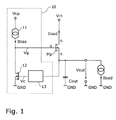
- Figure 1 shows a simple voltage regulator using a power MOSFET Mp as a voltage regulating element.
- a n-MOS transistor is used whose drain terminal D is connected to a first supply terminal receiving an input voltage Vin and whose source terminal S is connected to an output terminal providing an output voltage Vout and a load current Iload.
- a capacitance Cout is connected between the source terminal S and a second supply terminal, e.g. a ground terminal GND.
- the voltage regulator further comprises a feedback circuit 10 for regulating the output voltage Vout, i.e. the source potential of the power MOSFET, to a desired (e.g. constant) value.
- the feedback circuit 10 comprises a controller 13 whose input is connected to the source terminal S and responsive to the output voltage Vout.
- the output of the controller 13 provides a controller voltage Vc received by the gate of a controlling transistor 12 whose source terminal is connected to the ground terminal GND and whose drain terminal is connected to the gate G of the voltage regulating power MOSFET Mp and to a current source 11 providing a bias current Ibias to the gate G and to the controlling transistor 12.
- the current source 11 is connected to a third supply terminal receiving a supply voltage Vcp provided by a charge pump (not shown).
- FIG. 4 illustrates the step response of the output voltage Vout, the controller voltage Vc, and the gate voltage Vg to an upward step of the load current Iload.
- the drain-source voltage Vds of the power MOSFET Mp has been adjusted by the feedback circuit 10 such, that drain-source voltage Vds (i.e. the product RDS ⁇ Iload of the drain-source resistance RDS and the load current Iload) is equal to the difference between the supply voltage Vin and the output voltage Vout.
- An upward step of the load current Iload firstly results in a drop of the output voltage Vout.
- the controller 13 reduces the controller voltage Vc, i.e. the gate voltage of the controlling transistor 12, thus increasing the fractional part of the bias current Ibias used for charging the gate (i.e. the gate-source-capacitance) of the power MOSFET Mp.
- An increased gate charge results in a higher gate voltage Vg of the power MOSFET and in a lower drain-source voltage Vds (i.e. in a lower drain-source resistance RDS) which compensates for the higher load current Iload, thus readjusting the output voltage to its desired (constant) value.
- the time which is needed to readjust the drop in the output voltage Vout to its desired constant value depends on the time the feedback circuit 10 needs to react to a drop in the output voltage, i.e. the loop delay time tL, the time which is needed to charge the gate-source capacitance of the power MOSFET Mp, i.e. the charging time tC.
- the loop delay time tL depends on the bandwidth of the feedback circuit 10 and is usually much smaller than the charging time tC.
- To decrease the overall delay time tD (TD tL + tC) it is necessary to reduce the charging time tC, which could be done by increasing the bias current Ibias which would entail higher costs for the current source 11 and the charge pump.
- FIG. 2 Another possibility to improve the overall delay tD time without the need for increasing the bias current Ibias is shown in figure 2 .
- a current measurement means 30 is connected in series to the drain-source path of the power MOSFET Mp.
- the current measurement means is connected between the drain terminal D of the power MOSFET Mp and the supply terminal receiving Vin.
- the current measurement means 30 provides a measurement signal S30 which depends on the load current Iload.
- the voltage regulator further comprises a switching circuit 20 being responsive to the load current Iload (or, strictly speaking, to the measurement signal S30).
- the switching circuit 20 is connected to the output terminal providing the output voltage Vout (i.e. the source potential) and with the bulk terminal B of the power MOSFET Mp.
- the switching circuit comprises a switch SW responsive to the measurement signal S30.
- the switch SW is adapted for connecting the bulk terminal B of the power MOSFET Mp with either the source terminal S or a constant potential V2 dependent on the value of the load current Iload or the measurement signal S30 respectively.
- the constant potential V2 is preferably lower than the output voltage Vout and can also be equal to ground potential GND.
- An "ordinary" MOSFET would have its bulk terminal B connected to its source terminal S.
- the threshold voltage of the power MOSFET Mp increases, if the switch SW connects the bulk terminal B of the power MOSFET Mp with the constant potential V2 being lower than the source potential (Vout) of the power MOSFET Mp.
- This state of the switch SW is further referred to as the second switching state.
- the function of the circuit is explained in more detail by reference to figures 3 and 5 .
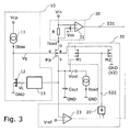
- FIG. 3 shows the embodiment of figure 2 wherein the measurement means 13 and the switching circuit 20 are illustrated in more detail.
- the measurement circuit 13 comprises a shunt resistor R, a voltage source providing the offset voltage Vos and a comparator 31.
- the shunt resistor is connected to the drain terminal D of the power MOSFET Mp with its first terminal in series to the drain-source path of the power MOSFET.
- a second terminal of the shunt resistor R is connected to a non-inverting input of the comparator 31 and the first terminal of the shunt resistor R is also connected to the inverting input of the comparator 31 via the voltage source providing the offset voltage Vos.
- the output signal of the comparator assumes a first logic level, e.g.
- the switching 20 circuit comprises a comparator 23, an AND-gate 22 with an inverting and a non-inverting input, and transistors M1, M2 provide the functionality of the switch SW.
- the comparator 23 is adapted for comparing the output voltage Vout with a reference voltage Vref and for providing an output signal which assumes a first logic level, e.g. a high level, if the output voltage is higher than the reference voltage.
- the output of the comparator 23 is connected with the non-inverting input of the AND-gate 22.
- the inverting input of the AND-gate 22 is connected with the output of the comparator 31 which has been described above.
- the AND-gate 22 provides a switching signal S22 controlling the switching states of the transistors M1, M2.
- the switching signal S22 assumes a first logic level, e.g. a high level, if the load current Iload is lower than a reference current defined by the quotient Vos/R and the output voltage is higher than the reference voltage Vref. Then the first p-MOS transistor M1 is switched to an off-state and the n-MOS transistor M2 is switched to an on-state, thus isolating the bulk terminal B of the power MOSFET Mp from the output terminal providing the output voltage Vout (and also from its source terminal S) and connecting the bulk terminal B of the power MOSFET Mp with the constant potential V2 which is - in the current case - equal to the ground potential.
- a first logic level e.g. a high level
- the output logic level of one of the comparators 23, 31 will change and the output signal S22 of the AND-gate 22 will switch to a second logic level, e.g. a low level, thus switching on the p-MOS transistor M1 and switching off the n-MOS transistor M2 and the p-MOS transistor M3.
- the bulk terminal B of the power MOSFET Mp is than connected to the source terminal S of the power MOSFET Mp and isolated from the constant potential V2.
- FIG. 5 shows, like figure 4 , timing diagrams of the load current Iload, the output voltage Vout, the control voltage Vc, the gate voltage Vg, and the bulk voltage Vb.
- the feedback circuit 10 can react much faster for regulating the output voltage Vout to its desired constant value and the charging time tC is greatly reduced, thus improving the overall performance of the voltage regulator.
Landscapes
- Engineering & Computer Science (AREA)
- Physics & Mathematics (AREA)
- Electromagnetism (AREA)
- General Physics & Mathematics (AREA)
- Radar, Positioning & Navigation (AREA)
- Automation & Control Theory (AREA)
- Continuous-Control Power Sources That Use Transistors (AREA)
Abstract
Description
- The present invention relates to voltage regulators, especially to voltage regulators having a low voltage drop, a low current consumption and a fast transient response.
- A low voltage drop over the voltage regulator is achieved by the use of a MOSFET as a voltage regulating element together with a charge pump providing a sufficiently high gate potential which has to be higher than the output voltage of the voltage regulator, in the case of a low drop regulator even higher than the input voltage of the voltage regulator.
- In order to guarantee a substantially constant output voltage, the gate of the voltage regulating MOSFET (e.g. a power MOSFET) is supplied with a bias current provided by a charge pump and controlled by a closed loop control system. That is, the output voltage of the voltage regulator is received by a controller which controls the gate current (and therefore the gate voltage) of the voltage regulating MOSFET such, that the output voltage of the voltage regulator remains substantially constant.
- In response to an upward step of the load current (i.e. the output current) the output voltage will slightly drop due to the higher voltage drop over the voltage regulating MOSFET. Triggered by this voltage drop the controller will increase the gate current for charging the gate-source-capacitance of the voltage regulating MOSFET in order to increase the conductivity of the voltage regulating MOSFET thus re-adjusting the output voltage to its desired value.
- The time which is needed to compensate for the disturbance in the output voltage induced by the step in a load current is determined by the loop bandwidth of the closed loop control system and especially dependent on the value of the gate-source-capacitance of the voltage regulating MOSFET.
- With a given value of the gate-source-capacitance of the voltage regulating MOSFET the speed of the closed loop control system can only be increased by increasing the gate current which charges the gate of the MOSFET. This gate current is supplied by a charge pump, as explained before, and, in order to minimize power consumption, an increase of the maximum gate current which would entail a more costly charge pump is not desirable.
- It is an object of the current invention to provide an improved voltage regulator which is able to compensate for disturbances in its output voltage induced by changes in the load current very quickly.
- This object is achieved by the voltage regulator of claim 1 and by the method for controlling a field effect transistor of claim 8. Several embodiments and enhancements of the invention are covered by the dependent claims.
- In one embodiment of the invention the inventive voltage regulator comprises a power filed effect transistor having a threshold voltage, a drain terminal receiving an input voltage, a source terminal providing an output voltage and a load current, a gate terminal responsive to a control signal, and a bulk terminal. The voltage regulator further comprises a control loop circuits responsive to the output voltage and providing the control signal. The control loop circuit is adapted for adjusting said control signal to such a value that the output voltage is regulated to a desired (constant) value. Additionally the threshold voltage of the power field effect transistor is modified dependent on the load current. Alternatively the threshold voltage can be modified dependent on the output voltage or on both, the output voltage and the load current.
- In another embodiment of the invention the voltage regulator additionally comprises a switching circuit for modifying the threshold voltage. The switching circuit is responsive to the output voltage and/or to the load current and it is adapted for connecting the bulk terminal of the field effect transistor with either the source terminal or a constant potential dependent on the load currents and/or the output voltage.
- The invention also comprises a method for controlling the power field effect transistor which was defined above. In one embodiment the method comprises the step of modifying the threshold voltage dependent on the load current and/or the output voltage. This can be done, for example, by a connecting the bulk terminal of the field effect transistor with either the source terminal or a constant potential dependent on the load current and/or the output voltage.
- The following discussion explains the invention in more detail based on the figures.
- Figure 1
- shows a conventional voltage regulator with a power MOSFET as a regulating element and a feedback circuit for regulating the output voltage to a desired constant value.
- Figure 2
- shows one embodiment of the inventive voltage regulator comprising a switching circuit for modifying the threshold voltage of the voltage regulating power MOSFET.
- Figure 3
- shows the embodiment of
figure 2 with the switching circuit being illustrated in more detail. - Figure 4
- shows timing diagrams of the load current, the output voltage and the gate voltage illustrating the step response of a voltage regulator according to
figure 1 . - Figure 5
- shows timing diagrams of the load current, the output voltage, the gate voltage and the bulk voltage illustrating the step response of an inventive voltage regulator according to
figure 2 or3 . - In the figures, unless otherwise indicated, the same reference notations refer to the same components or the same signals with the same meaning.
-
Figure 1 shows a simple voltage regulator using a power MOSFET Mp as a voltage regulating element. In the embodiment shown infigure 1 a n-MOS transistor is used whose drain terminal D is connected to a first supply terminal receiving an input voltage Vin and whose source terminal S is connected to an output terminal providing an output voltage Vout and a load current Iload. For compensating for high frequency current spikes a capacitance Cout is connected between the source terminal S and a second supply terminal, e.g. a ground terminal GND. The voltage regulator further comprises afeedback circuit 10 for regulating the output voltage Vout, i.e. the source potential of the power MOSFET, to a desired (e.g. constant) value. - The
feedback circuit 10 comprises acontroller 13 whose input is connected to the source terminal S and responsive to the output voltage Vout. The output of thecontroller 13 provides a controller voltage Vc received by the gate of a controllingtransistor 12 whose source terminal is connected to the ground terminal GND and whose drain terminal is connected to the gate G of the voltage regulating power MOSFET Mp and to acurrent source 11 providing a bias current Ibias to the gate G and to the controllingtransistor 12. Thecurrent source 11 is connected to a third supply terminal receiving a supply voltage Vcp provided by a charge pump (not shown). - The function of the feedback circuit can be easily understood with the help of the timing diagrams shown in
figure 4. Figure 4 illustrates the step response of the output voltage Vout, the controller voltage Vc, and the gate voltage Vg to an upward step of the load current Iload. In the circuit offigure 1 with a given output voltage Vout, a given load current Iload, and a given supply voltage Vin the drain-source voltage Vds of the power MOSFET Mp has been adjusted by thefeedback circuit 10 such, that drain-source voltage Vds (i.e. the product RDS × Iload of the drain-source resistance RDS and the load current Iload) is equal to the difference between the supply voltage Vin and the output voltage Vout. An upward step of the load current Iload firstly results in a drop of the output voltage Vout. Triggered by this voltage drop thecontroller 13 reduces the controller voltage Vc, i.e. the gate voltage of the controllingtransistor 12, thus increasing the fractional part of the bias current Ibias used for charging the gate (i.e. the gate-source-capacitance) of the power MOSFET Mp. An increased gate charge results in a higher gate voltage Vg of the power MOSFET and in a lower drain-source voltage Vds (i.e. in a lower drain-source resistance RDS) which compensates for the higher load current Iload, thus readjusting the output voltage to its desired (constant) value. - The time which is needed to readjust the drop in the output voltage Vout to its desired constant value depends on the time the
feedback circuit 10 needs to react to a drop in the output voltage, i.e. the loop delay time tL, the time which is needed to charge the gate-source capacitance of the power MOSFET Mp, i.e. the charging time tC. The loop delay time tL depends on the bandwidth of thefeedback circuit 10 and is usually much smaller than the charging time tC. To decrease the overall delay time tD (TD = tL + tC) it is necessary to reduce the charging time tC, which could be done by increasing the bias current Ibias which would entail higher costs for thecurrent source 11 and the charge pump. - Another possibility to improve the overall delay tD time without the need for increasing the bias current Ibias is shown in
figure 2 . compared to the circuit offigure 1 a current measurement means 30 is connected in series to the drain-source path of the power MOSFET Mp. In the case offigure 2 the current measurement means is connected between the drain terminal D of the power MOSFET Mp and the supply terminal receiving Vin. The current measurement means 30 provides a measurement signal S30 which depends on the load current Iload. The voltage regulator further comprises aswitching circuit 20 being responsive to the load current Iload (or, strictly speaking, to the measurement signal S30). Theswitching circuit 20 is connected to the output terminal providing the output voltage Vout (i.e. the source potential) and with the bulk terminal B of the power MOSFET Mp. The switching circuit comprises a switch SW responsive to the measurement signal S30. The switch SW is adapted for connecting the bulk terminal B of the power MOSFET Mp with either the source terminal S or a constant potential V2 dependent on the value of the load current Iload or the measurement signal S30 respectively. - The constant potential V2 is preferably lower than the output voltage Vout and can also be equal to ground potential GND. An "ordinary" MOSFET would have its bulk terminal B connected to its source terminal S. Compared to this switching state (a first switching state) the threshold voltage of the power MOSFET Mp increases, if the switch SW connects the bulk terminal B of the power MOSFET Mp with the constant potential V2 being lower than the source potential (Vout) of the power MOSFET Mp. This state of the switch SW is further referred to as the second switching state. The function of the circuit is explained in more detail by reference to
figures 3 and5 . -
Figure 3 shows the embodiment offigure 2 wherein the measurement means 13 and theswitching circuit 20 are illustrated in more detail. Themeasurement circuit 13 comprises a shunt resistor R, a voltage source providing the offset voltage Vos and acomparator 31. The shunt resistor is connected to the drain terminal D of the power MOSFET Mp with its first terminal in series to the drain-source path of the power MOSFET. A second terminal of the shunt resistor R is connected to a non-inverting input of thecomparator 31 and the first terminal of the shunt resistor R is also connected to the inverting input of thecomparator 31 via the voltage source providing the offset voltage Vos. The output signal of the comparator assumes a first logic level, e.g. a high level, if the load current Iload is higher than a reference current defined by the quotient Iref=Vos/R of the shunt resistor R and the offset voltage Vos. Of course any other method for measuring the load current Iload and comparing it with a reference current is applicable (e.g. a sense-FET). - Additionally to the embodiment shown in
figure 2 the switching 20 circuit comprises acomparator 23, an AND-gate 22 with an inverting and a non-inverting input, and transistors M1, M2 provide the functionality of the switch SW. Thecomparator 23 is adapted for comparing the output voltage Vout with a reference voltage Vref and for providing an output signal which assumes a first logic level, e.g. a high level, if the output voltage is higher than the reference voltage. The output of thecomparator 23 is connected with the non-inverting input of the AND-gate 22. The inverting input of the AND-gate 22 is connected with the output of thecomparator 31 which has been described above. The AND-gate 22 provides a switching signal S22 controlling the switching states of the transistors M1, M2. - In the current embodiment the switching signal S22 assumes a first logic level, e.g. a high level, if the load current Iload is lower than a reference current defined by the quotient Vos/R and the output voltage is higher than the reference voltage Vref. Then the first p-MOS transistor M1 is switched to an off-state and the n-MOS transistor M2 is switched to an on-state, thus isolating the bulk terminal B of the power MOSFET Mp from the output terminal providing the output voltage Vout (and also from its source terminal S) and connecting the bulk terminal B of the power MOSFET Mp with the constant potential V2 which is - in the current case - equal to the ground potential.
- If either the output voltage drops below the reference voltage Vref or the load current rises above the reference current defined by the quotient Vos/R the output logic level of one of the
comparators - Connecting the bulk terminal either with a constant potential V2 or with the source terminal S will change the threshold voltage of the voltage regulating power MOSFET Mp. The effect of this change of the threshold voltage on the speed of the feedback circuit can easily be explained by the help of
figure 5. Figure 5 shows, likefigure 4 , timing diagrams of the load current Iload, the output voltage Vout, the control voltage Vc, the gate voltage Vg, and the bulk voltage Vb. The left hand side of the timing diagram of Iload shows the load current Iload dropping below the reference current Iref = Vout/R. As a consequence the bulk terminal B is isolated from the source terminal S and connected with a constant potential V2. This results in an increase of the threshold voltage of the power MOSFET Mp and the controller 13 (via the controlling transistor 12) has to adjust the gate voltage Vg to a higher value, i.e the gate G of the power MOSFET Mp is precharged during the second switching state when the load current Iload is below the reference current and the output voltage Vout is above the reference voltage Vref. In response to an upward step in the load current Iref a drop in the output voltage Vout will be observed. Due to the rise of the load current Iload the bulk terminal B of the power MOSFET Mp will again be connected with the source terminal S and therefore the threshold voltage of the power MOSFET Mp is decreased again. Due to the fact, that the gate G of the power MOSFET Mp was precharged before, less charge is necessary to increase the gate voltage to a value necessary for compensating for the increase load current. As a consequence thefeedback circuit 10 can react much faster for regulating the output voltage Vout to its desired constant value and the charging time tC is greatly reduced, thus improving the overall performance of the voltage regulator.
Claims (12)
- A voltage regulator comprising- a power field effect transistor (Mp) having a threshold voltage (Vth), a drain terminal receiving an input voltage (Vin), a source terminal providing an output voltage (Vout) and a load current (Iload), a gate terminal responsive to a control signal (Vg), and a bulk terminal,- a control-loop circuit (10) responsive to said output voltage (Vout) and providing said control signal (Vg), said control circuit being adapted for adjusting said control (Vg) signal to such a value that said output voltage (Vout) is regulated to a constant value,wherein said threshold voltage (Vth) of said power field effect transistor (Mp) is modified dependent on said load current (Iload).
- The voltage regulator of claim 1 further comprising a switching circuit (20) responsive to said output voltage (Vout) and to said load current (Iload), said switching circuit being adapted for connecting said bulk terminal with said source terminal or with a constant potential (V2) dependent on said load current and/or said output voltage.
- The voltage regulator of claim 2, wherein said switching circuit (20) is adapted for- connecting said bulk terminal (B) with said source terminal (S), if said load current (Iload) is higher than a reference current, and for- connecting said bulk terminal (B) with said constant potential (V2), if said load current (Iload) is lower than said reference current.
- The voltage regulator of claim 2, wherein said switching circuit (20) is adapted for- connecting said bulk terminal (B) with said source terminal (S), if said output voltage is lower than a reference voltage, and for- connecting said bulk terminal (B) with said constant potential (V2), if said said output voltage is higher than said reference voltage.
- The voltage regulator of claim 2, wherein said switching circuit (20) is adapted for- connecting said bulk terminal (B) with said source terminal (S), if said load current (Iload) is higher than a reference current and said output voltage is lower than a reference voltage, and for- connecting said bulk terminal (B) with said constant potential (V2), if said load current (Iload) is lower than said reference current and said output voltage is higher than said reference voltage.
- The voltage regulator of claim 3, 4, or 5, wherein said constant potential (V2) is lower than said output voltage (Vout).
- The voltage regulator of claim 3, 4, or 5, wherein said said constant potential (V2) is equal to a ground potential (GND).
- A method for controlling a power field effect transistor (Mp) having a threshold voltage (Vth), a drain terminal receiving an input voltage (Vin), a source terminal providing an output voltage (Vout) and a load current (Iload), a gate terminal responsive to a control signal (Vg), and a bulk terminal; said method comprising- modifying said threshold voltage dependent on said load current (Iload) and/or said output voltage (Vout).
- The method of claim 8 further comprising:- connecting said bulk terminal with said source terminal or with a constant potential (V2) dependent on said load current.
- The method of claim.9 further comprising:- comparing said load current (Iload) with a reference current,- connecting said bulk terminal with said source terminal, if said load current (Iload) is higher than said reference current, or connecting said bulk terminal with a constant potential (V2), if said load current (Iload) is lower than said reference current.
- The method of claim 9 further comprising:- comparing said output voltage (Vout) with a reference voltage,- connecting said bulk terminal with said source terminal, if said output voltage (Vout) is lower than said reference voltage, or connecting said bulk terminal with a constant potential (V2), if said output voltage (Vout) is higher than said reference voltage.
- The method of claim 9 further comprising:- comparing said load current (Iload) with a reference current,- comparing said output voltage (Vout) with a reference voltage,- connecting said bulk terminal with said source terminal, if said load current (Iload) is higher than said reference current and said output voltage (Vout) is lower than said reference voltage, or connecting said bulk terminal with a constant potential (V2), if said load current (Iload) is lower than said reference current and if said output voltage (Vout) is higher than said reference voltage.
Priority Applications (1)
| Application Number | Priority Date | Filing Date | Title |
|---|---|---|---|
| EP20060025990 EP1933221B1 (en) | 2006-12-14 | 2006-12-14 | Voltage regulator with an improved transient response |
Applications Claiming Priority (1)
| Application Number | Priority Date | Filing Date | Title |
|---|---|---|---|
| EP20060025990 EP1933221B1 (en) | 2006-12-14 | 2006-12-14 | Voltage regulator with an improved transient response |
Publications (2)
| Publication Number | Publication Date |
|---|---|
| EP1933221A1 true EP1933221A1 (en) | 2008-06-18 |
| EP1933221B1 EP1933221B1 (en) | 2012-03-21 |
Family
ID=37762481
Family Applications (1)
| Application Number | Title | Priority Date | Filing Date |
|---|---|---|---|
| EP20060025990 Ceased EP1933221B1 (en) | 2006-12-14 | 2006-12-14 | Voltage regulator with an improved transient response |
Country Status (1)
| Country | Link |
|---|---|
| EP (1) | EP1933221B1 (en) |
Cited By (5)
| Publication number | Priority date | Publication date | Assignee | Title |
|---|---|---|---|---|
| US8253479B2 (en) | 2009-11-19 | 2012-08-28 | Freescale Semiconductor, Inc. | Output driver circuits for voltage regulators |
| DE102018131859B3 (en) | 2018-12-12 | 2020-04-30 | Semikron Elektronik Gmbh & Co. Kg Patentabteilung | Power semiconductor device with a power semiconductor switch and with a control device |
| CN114448237A (en) * | 2021-12-06 | 2022-05-06 | 深圳市创芯微微电子有限公司 | A DC switching power supply and its fast transient response circuit |
| CN114637355A (en) * | 2020-12-15 | 2022-06-17 | 炬芯科技股份有限公司 | Voltage stabilizing circuit and voltage stabilizing control method |
| CN114740934A (en) * | 2022-04-29 | 2022-07-12 | 北京时代民芯科技有限公司 | A Large Drive Balanced LDO Circuit |
Citations (3)
| Publication number | Priority date | Publication date | Assignee | Title |
|---|---|---|---|---|
| US20020185681A1 (en) * | 2001-06-06 | 2002-12-12 | Takashi Nakano | Power MOS transistor having capability for setting substrate potential independently of source potential |
| US6744288B1 (en) * | 2002-10-15 | 2004-06-01 | National Semiconductor Corporation | Driver with bulk switching MOS power transistor |
| US20040239304A1 (en) * | 2003-06-02 | 2004-12-02 | Perez Raul A. | Threshold voltage adjustment for MOS devices |
-
2006
- 2006-12-14 EP EP20060025990 patent/EP1933221B1/en not_active Ceased
Patent Citations (3)
| Publication number | Priority date | Publication date | Assignee | Title |
|---|---|---|---|---|
| US20020185681A1 (en) * | 2001-06-06 | 2002-12-12 | Takashi Nakano | Power MOS transistor having capability for setting substrate potential independently of source potential |
| US6744288B1 (en) * | 2002-10-15 | 2004-06-01 | National Semiconductor Corporation | Driver with bulk switching MOS power transistor |
| US20040239304A1 (en) * | 2003-06-02 | 2004-12-02 | Perez Raul A. | Threshold voltage adjustment for MOS devices |
Non-Patent Citations (1)
| Title |
|---|
| GABRIEL A RINCON-MORA ET AL: "A Low-Voltage, Low Quiescent Current, Low Drop-Out Regulator", IEEE JOURNAL OF SOLID-STATE CIRCUITS, IEEE SERVICE CENTER, PISCATAWAY, NJ, US, vol. 33, no. 1, January 1998 (1998-01-01), XP011060653, ISSN: 0018-9200 * |
Cited By (7)
| Publication number | Priority date | Publication date | Assignee | Title |
|---|---|---|---|---|
| US8253479B2 (en) | 2009-11-19 | 2012-08-28 | Freescale Semiconductor, Inc. | Output driver circuits for voltage regulators |
| DE102018131859B3 (en) | 2018-12-12 | 2020-04-30 | Semikron Elektronik Gmbh & Co. Kg Patentabteilung | Power semiconductor device with a power semiconductor switch and with a control device |
| CN114637355A (en) * | 2020-12-15 | 2022-06-17 | 炬芯科技股份有限公司 | Voltage stabilizing circuit and voltage stabilizing control method |
| CN114637355B (en) * | 2020-12-15 | 2023-08-29 | 炬芯科技股份有限公司 | Voltage stabilizing circuit and voltage stabilizing control method |
| CN114448237A (en) * | 2021-12-06 | 2022-05-06 | 深圳市创芯微微电子有限公司 | A DC switching power supply and its fast transient response circuit |
| CN114740934A (en) * | 2022-04-29 | 2022-07-12 | 北京时代民芯科技有限公司 | A Large Drive Balanced LDO Circuit |
| CN114740934B (en) * | 2022-04-29 | 2024-04-05 | 北京时代民芯科技有限公司 | A large drive balanced LDO circuit |
Also Published As
| Publication number | Publication date |
|---|---|
| EP1933221B1 (en) | 2012-03-21 |
Similar Documents
| Publication | Publication Date | Title |
|---|---|---|
| KR101508391B1 (en) | Voltage regulator | |
| US8575906B2 (en) | Constant voltage regulator | |
| US7652455B2 (en) | Low-dropout voltage regulator with a voltage slew rate efficient transient response boost circuit | |
| US20230221746A1 (en) | High-speed low-impedance boosting low-dropout regulator | |
| US10452087B2 (en) | Low drop-out regulator | |
| US8810219B2 (en) | Voltage regulator with transient response | |
| US7855535B2 (en) | Inrush current control | |
| US7589509B2 (en) | Switching regulator | |
| US8525580B2 (en) | Semiconductor circuit and constant voltage regulator employing same | |
| US20110193538A1 (en) | Domino voltage regulator (dvr) | |
| EP3051378B1 (en) | Low dropout regulator circuit and method for controlling a voltage of a low dropout regulator circuit | |
| US20030147193A1 (en) | Voltage regulator protected against short -circuits | |
| US10338617B2 (en) | Regulator circuit | |
| US20160161961A1 (en) | Circuit to improve load transient behavior of voltage regulators and load switches | |
| US7446514B1 (en) | Linear regulator for use with electronic circuits | |
| US10175708B2 (en) | Power supply device | |
| CN103383581B (en) | A voltage regulator with transient response enhancement mechanism | |
| US9817427B2 (en) | Static offset reduction in a current conveyor | |
| US7589510B2 (en) | Voltage regulator having variable threshold voltage switch | |
| US10063132B1 (en) | Over-current protection circuit | |
| US20130063115A1 (en) | Constant-voltage power supply circuit | |
| US8981840B1 (en) | Reduction in on-resistance in pass device | |
| EP1933221B1 (en) | Voltage regulator with an improved transient response | |
| US9933798B2 (en) | Voltage regulator | |
| KR100967029B1 (en) | Regulator with Soft Start |
Legal Events
| Date | Code | Title | Description |
|---|---|---|---|
| PUAI | Public reference made under article 153(3) epc to a published international application that has entered the european phase |
Free format text: ORIGINAL CODE: 0009012 |
|
| 17P | Request for examination filed |
Effective date: 20070512 |
|
| AK | Designated contracting states |
Kind code of ref document: A1 Designated state(s): AT BE BG CH CY CZ DE DK EE ES FI FR GB GR HU IE IS IT LI LT LU LV MC NL PL PT RO SE SI SK TR |
|
| AX | Request for extension of the european patent |
Extension state: AL BA HR MK RS |
|
| APBK | Appeal reference recorded |
Free format text: ORIGINAL CODE: EPIDOSNREFNE |
|
| APBN | Date of receipt of notice of appeal recorded |
Free format text: ORIGINAL CODE: EPIDOSNNOA2E |
|
| AKX | Designation fees paid |
Designated state(s): DE FR GB IT |
|
| APBR | Date of receipt of statement of grounds of appeal recorded |
Free format text: ORIGINAL CODE: EPIDOSNNOA3E |
|
| APAF | Appeal reference modified |
Free format text: ORIGINAL CODE: EPIDOSCREFNE |
|
| RAP1 | Party data changed (applicant data changed or rights of an application transferred) |
Owner name: INFINEON TECHNOLOGIES AG |
|
| APBT | Appeal procedure closed |
Free format text: ORIGINAL CODE: EPIDOSNNOA9E |
|
| GRAJ | Information related to disapproval of communication of intention to grant by the applicant or resumption of examination proceedings by the epo deleted |
Free format text: ORIGINAL CODE: EPIDOSDIGR1 |
|
| GRAP | Despatch of communication of intention to grant a patent |
Free format text: ORIGINAL CODE: EPIDOSNIGR1 |
|
| GRAP | Despatch of communication of intention to grant a patent |
Free format text: ORIGINAL CODE: EPIDOSNIGR1 |
|
| GRAS | Grant fee paid |
Free format text: ORIGINAL CODE: EPIDOSNIGR3 |
|
| GRAA | (expected) grant |
Free format text: ORIGINAL CODE: 0009210 |
|
| AK | Designated contracting states |
Kind code of ref document: B1 Designated state(s): DE FR GB IT |
|
| REG | Reference to a national code |
Ref country code: GB Ref legal event code: FG4D |
|
| REG | Reference to a national code |
Ref country code: DE Ref legal event code: R096 Ref document number: 602006028276 Country of ref document: DE Effective date: 20120516 |
|
| PLBE | No opposition filed within time limit |
Free format text: ORIGINAL CODE: 0009261 |
|
| STAA | Information on the status of an ep patent application or granted ep patent |
Free format text: STATUS: NO OPPOSITION FILED WITHIN TIME LIMIT |
|
| 26N | No opposition filed |
Effective date: 20130102 |
|
| REG | Reference to a national code |
Ref country code: DE Ref legal event code: R097 Ref document number: 602006028276 Country of ref document: DE Effective date: 20130102 |
|
| REG | Reference to a national code |
Ref country code: FR Ref legal event code: PLFP Year of fee payment: 10 |
|
| REG | Reference to a national code |
Ref country code: FR Ref legal event code: PLFP Year of fee payment: 11 |
|
| REG | Reference to a national code |
Ref country code: FR Ref legal event code: PLFP Year of fee payment: 12 |
|
| PGFP | Annual fee paid to national office [announced via postgrant information from national office to epo] |
Ref country code: DE Payment date: 20220225 Year of fee payment: 16 |
|
| PGFP | Annual fee paid to national office [announced via postgrant information from national office to epo] |
Ref country code: GB Payment date: 20221222 Year of fee payment: 17 Ref country code: FR Payment date: 20221222 Year of fee payment: 17 |
|
| PGFP | Annual fee paid to national office [announced via postgrant information from national office to epo] |
Ref country code: IT Payment date: 20221228 Year of fee payment: 17 |
|
| REG | Reference to a national code |
Ref country code: DE Ref legal event code: R119 Ref document number: 602006028276 Country of ref document: DE |
|
| PG25 | Lapsed in a contracting state [announced via postgrant information from national office to epo] |
Ref country code: DE Free format text: LAPSE BECAUSE OF NON-PAYMENT OF DUE FEES Effective date: 20230701 |
|
| GBPC | Gb: european patent ceased through non-payment of renewal fee |
Effective date: 20231214 |
|
| PG25 | Lapsed in a contracting state [announced via postgrant information from national office to epo] |
Ref country code: GB Free format text: LAPSE BECAUSE OF NON-PAYMENT OF DUE FEES Effective date: 20231214 |
|
| PG25 | Lapsed in a contracting state [announced via postgrant information from national office to epo] |
Ref country code: FR Free format text: LAPSE BECAUSE OF NON-PAYMENT OF DUE FEES Effective date: 20231231 |
|
| PG25 | Lapsed in a contracting state [announced via postgrant information from national office to epo] |
Ref country code: GB Free format text: LAPSE BECAUSE OF NON-PAYMENT OF DUE FEES Effective date: 20231214 Ref country code: FR Free format text: LAPSE BECAUSE OF NON-PAYMENT OF DUE FEES Effective date: 20231231 |
|
| PG25 | Lapsed in a contracting state [announced via postgrant information from national office to epo] |
Ref country code: IT Free format text: LAPSE BECAUSE OF NON-PAYMENT OF DUE FEES Effective date: 20231214 |