EP1930940A1 - Organic thin film transistor, and method for surface modification of gate insulating layer in organic thin film transistor - Google Patents
Organic thin film transistor, and method for surface modification of gate insulating layer in organic thin film transistor Download PDFInfo
- Publication number
- EP1930940A1 EP1930940A1 EP06783033A EP06783033A EP1930940A1 EP 1930940 A1 EP1930940 A1 EP 1930940A1 EP 06783033 A EP06783033 A EP 06783033A EP 06783033 A EP06783033 A EP 06783033A EP 1930940 A1 EP1930940 A1 EP 1930940A1
- Authority
- EP
- European Patent Office
- Prior art keywords
- thin film
- organic thin
- film transistor
- gate insulating
- insulating layer
- Prior art date
- Legal status (The legal status is an assumption and is not a legal conclusion. Google has not performed a legal analysis and makes no representation as to the accuracy of the status listed.)
- Withdrawn
Links
Images









Classifications
-
- H—ELECTRICITY
- H10—SEMICONDUCTOR DEVICES; ELECTRIC SOLID-STATE DEVICES NOT OTHERWISE PROVIDED FOR
- H10K—ORGANIC ELECTRIC SOLID-STATE DEVICES
- H10K10/00—Organic devices specially adapted for rectifying, amplifying, oscillating or switching; Organic capacitors or resistors having potential barriers
- H10K10/40—Organic transistors
- H10K10/46—Field-effect transistors, e.g. organic thin-film transistors [OTFT]
- H10K10/462—Insulated gate field-effect transistors [IGFETs]
- H10K10/466—Lateral bottom-gate IGFETs comprising only a single gate
-
- H—ELECTRICITY
- H10—SEMICONDUCTOR DEVICES; ELECTRIC SOLID-STATE DEVICES NOT OTHERWISE PROVIDED FOR
- H10K—ORGANIC ELECTRIC SOLID-STATE DEVICES
- H10K10/00—Organic devices specially adapted for rectifying, amplifying, oscillating or switching; Organic capacitors or resistors having potential barriers
- H10K10/40—Organic transistors
- H10K10/46—Field-effect transistors, e.g. organic thin-film transistors [OTFT]
- H10K10/462—Insulated gate field-effect transistors [IGFETs]
- H10K10/468—Insulated gate field-effect transistors [IGFETs] characterised by the gate dielectrics
- H10K10/472—Insulated gate field-effect transistors [IGFETs] characterised by the gate dielectrics the gate dielectric comprising only inorganic materials
-
- H—ELECTRICITY
- H10—SEMICONDUCTOR DEVICES; ELECTRIC SOLID-STATE DEVICES NOT OTHERWISE PROVIDED FOR
- H10K—ORGANIC ELECTRIC SOLID-STATE DEVICES
- H10K10/00—Organic devices specially adapted for rectifying, amplifying, oscillating or switching; Organic capacitors or resistors having potential barriers
- H10K10/40—Organic transistors
- H10K10/46—Field-effect transistors, e.g. organic thin-film transistors [OTFT]
- H10K10/462—Insulated gate field-effect transistors [IGFETs]
- H10K10/468—Insulated gate field-effect transistors [IGFETs] characterised by the gate dielectrics
- H10K10/474—Insulated gate field-effect transistors [IGFETs] characterised by the gate dielectrics the gate dielectric comprising a multilayered structure
- H10K10/476—Insulated gate field-effect transistors [IGFETs] characterised by the gate dielectrics the gate dielectric comprising a multilayered structure comprising at least one organic layer and at least one inorganic layer
-
- H—ELECTRICITY
- H10—SEMICONDUCTOR DEVICES; ELECTRIC SOLID-STATE DEVICES NOT OTHERWISE PROVIDED FOR
- H10K—ORGANIC ELECTRIC SOLID-STATE DEVICES
- H10K71/00—Manufacture or treatment specially adapted for the organic devices covered by this subclass
- H10K71/10—Deposition of organic active material
- H10K71/16—Deposition of organic active material using physical vapour deposition [PVD], e.g. vacuum deposition or sputtering
- H10K71/166—Deposition of organic active material using physical vapour deposition [PVD], e.g. vacuum deposition or sputtering using selective deposition, e.g. using a mask
-
- H—ELECTRICITY
- H10—SEMICONDUCTOR DEVICES; ELECTRIC SOLID-STATE DEVICES NOT OTHERWISE PROVIDED FOR
- H10K—ORGANIC ELECTRIC SOLID-STATE DEVICES
- H10K19/00—Integrated devices, or assemblies of multiple devices, comprising at least one organic element specially adapted for rectifying, amplifying, oscillating or switching, covered by group H10K10/00
- H10K19/10—Integrated devices, or assemblies of multiple devices, comprising at least one organic element specially adapted for rectifying, amplifying, oscillating or switching, covered by group H10K10/00 comprising field-effect transistors
-
- H—ELECTRICITY
- H10—SEMICONDUCTOR DEVICES; ELECTRIC SOLID-STATE DEVICES NOT OTHERWISE PROVIDED FOR
- H10K—ORGANIC ELECTRIC SOLID-STATE DEVICES
- H10K85/00—Organic materials used in the body or electrodes of devices covered by this subclass
- H10K85/60—Organic compounds having low molecular weight
- H10K85/615—Polycyclic condensed aromatic hydrocarbons, e.g. anthracene
- H10K85/623—Polycyclic condensed aromatic hydrocarbons, e.g. anthracene containing five rings, e.g. pentacene
Definitions
- the present invention relates to an organic thin film transistor and a method for surface modification of a gate insulating layer in the organic thin film transistor.
- an organic thin film transistor using an organic substance as a material uses an oxide, for example, as a gate insulating layer.
- various methods of performing surface modification of the gate insulating layer formed of an oxide have been proposed to improve its transistor characteristics.
- a method of performing surface modification of the gate insulating layer formed of the oxide a method of forming a self-assembled film such as octadecyltrichlorosilane (OTS) and 1,1,1,3,3,3-hexamethyldisilazane (HMDS), for example, has been mentioned.
- OTS octadecyltrichlorosilane
- HMDS 1,1,1,3,3,3-hexamethyldisilazane
- the above-described conventional method was limited to the case where the gate insulating layer is formed of an oxide, had a problems that it could not be applied to the case where the gate insulating layer was formed of a substance other than the oxide.
- Patent Document 1 Japanese Patent Laid-open No. 2003-255857 presented as Patent Document 1, for example.
- Non-patent Document 1 D.J.Gundlach, J.A.Nichols, L.Zhou and T.N.Jackson, Appl.Phys.Lett.80, 2925(2002 )
- Non-patent Document 2 M.Shtein, J.Mapel, J.B.Benziger and S.Forrest, Appl.Phys.Lett.81, 263(2002 )
- Non-patent Document 3 D.Knipp, R.A.Street, A.Volkel and J.Ho, J.Appl.Phys.93, 347(2003 )
- Non-patent Document 4 J.Lee, K. Kim, J.H.Kim, S. Im and D.
- Patent Document 1 Japanese Patent Laid-open No. 2003-255857
- the present invention has been created in view of the above-described problem that prior art has, and it is an object of the invention to provide an organic thin film transistor and a method for surface modification of the gate insulating layer of the organic thin film transistor, which is capable of modifying the surface of the gate insulating layer not only in the case where the gate insulating layer is formed of an oxide but also in the case where the gate insulating layer is formed of a substance other than the oxide, and consequently transistor characteristics can be significantly improved.
- the present invention is designed that a layer formed of polyparaxylylene (poly para-xylylene) is formed on the surface of the gate insulating layer.
- the formation of polyparaxylylene layer on the surface of the gate insulating layer should only be performed by depositing polyparaxylylene film on the surface of the gate insulating layer by using a chemical vapor deposition (CVD), for example.
- CVD chemical vapor deposition
- the surface of the gate insulating layer is modified to hydrophobic, a threshold voltage becomes negative, Off can be taken when a gate voltage is zero, and stable operation can be obtained as a transistor.
- the present invention is an organic thin film transistor where an organic semiconductor layer is stacked on a gate insulating layer and an electrode is formed on the organic semiconductor layer, in which a polyparaxylylene layer formed of a continuous polyparaxylylene film is formed on the surface of the gate insulating layer, between the gate insulating layer and the organic semiconductor layer, so as to face and contact the organic semiconductor layer.
- the polyparaxylylene film is a continuous film whose film thickness shows the angle of 85 degrees or more by contact angle measurement of water.
- the present invention in the above-described invention is designed that the polyparaxylylene has the purity of 99% or higher.
- the present invention in the above-described invention is designed that the thickness of the polyparaxylylene film is 5 to 200nm. Further, the present invention, in the above-described invention is designed that the polyparaxylylene is polychloroparaxylylene. Further, the present invention, in the method for surface modification of the gate insulating layer in the organic thin film transistor where the organic semiconductor layer is stacked on the gate insulating layer and the electrode is formed on the organic semiconductor layer is designed that the polyparaxylylene film is deposited on the surface of the gate insulating layer as continuous film having a predetermined thickness by chemical vapor deposition.
- the present invention in the above-described invention is designed that the film thickness of the continuous film shows the angle of 85 degrees or more by the contact angle evaluation of water. Further, the present invention, in the above-described invention is designed that the polyparaxylylene has the purity of 99% or higher. Further, the present invention, in the above-described invention is designed that the film thickness of the continuous film is 5 to 200nm. Further, the present invention, the above-described invention is designed that the polyparaxylylene is polychloroparaxylylene.
- the present invention is constituted as described above, the invention exerts an excellent effect that it can perform modification of the surface of the gate insulating layer not only in the case where the gate insulating layer is formed of an oxide but also in the case where the gate insulating layer is formed of a substance other than the oxide, and consequently transistor characteristics can be significantly improved.
- Fig.1 is a constitution explanatory view showing an example of an embodiment of the organic thin film transistor according to the present invention.
- an organic thin film transistor 10 is constituted by having: a substrate 12 formed of semiconductor, which is a gate layer that functions as a substrate and a gate electrode; a gate insulating layer 14 formed of an insulative material, which is formed on one surface 12a of the substrate 12; a polyparaxylylene film 16 being a polyparaxylylene layer, which is formed on the surface 14a of the gate insulating layer 14 by depositing polyparaxylylene; an organic semiconductor layer 18 being an active layer formed of an organic material, which is formed on the surface 16a of the polyparaxylylene film 16; a source electrode 20 being a first electrode formed of a conductive material, which is formed on the surface 18a of the organic semiconductor layer 18; and a drain electrode 22 being a second electrode formed of a conductive material, which is formed on the surface 18a of the organic semiconductor layer 18.
- the polyparaxylylene film 16 and the organic semiconductor layer 18 face and contact with each other, and the polyparaxylylene film 16 is arranged directly under the organic semiconductor layer 18.
- the polyparaxylylene film 16 and the organic semiconductor layer 18 should only be formed by deposition, for example.
- the substrate 12 an n-type Si substrate being an Si substrate doped with phosphorus can be used, for example, but the substrate is not limited to this, and an n-type semiconductor substrate or a p-type semiconductor substrate where various impurities are doped in various semiconductor materials can be used.
- an SiO 2 film being an insulative material can be used, for example, but the layer is not limited to this, and polymer film such as polyvinylphenol (PVP), polyvinylalcohol (PVA) and polystyrene (PS), for example, can be used instead of an oxide like SiO 2 .
- the polyparaxylylene film 16 is formed as a continuous film, that is, a continuous film having no holes formed therein, and it is preferable to form the film by high-purity polyparaxylylene, for example, more particularly polyparaxylylene whose purity is 99% or higher.
- the film thickness of the polyparaxylylene film is not particularly limited, it is preferable that the thickness be about 5 to 200nm, more particularly about 5 to 100nm. Particularly, in the case where the surface of the polyparaxylylene film 16 can be formed homogeneously, the film thickness can be made as thin as about 5nm, for example. It is to be noted that formation of a film whose surface is homogeneous is made possible by using high-purity polyparaxylylene. Furthermore, as an organic material for forming the organic semiconductor layer 18, pentacene (Pentacene) can be used for example, but the material is not limited to this, and various organic materials such as copper phthalocyanine and thiophenes can be used, for example.
- pentacene pentacene
- various organic materials such as copper phthalocyanine and thiophenes can be used, for example.
- the source electrode 20 and the drain electrode 22 can be formed by depositing metal being a conductive material which is Au, for example, by vapor deposition on the surface 18a of the organic semiconductor layer 18, for example, an Au electrode formed in this manner can be used as the source electrode 20 and the drain electrode 22.
- a conductive material used as the source electrode 20 and the drain electrode 22 is not limited to Au, but Pt, Ag or the like can be used.
- the polyparaxylylene film 16 modifies the surface of the gate insulating layer 14 from hydrophilic to hydrophobic, and consequently, the transistor characteristics of the organic thin film transistor 10 could be significantly improved.
- “dix-C” (trademark) on the surface of the SiO 2 thermal oxide film by chemical vapor deposition in this experiment, it was performed under reduced pressure by using an exclusive unit called “DACS-0" (trademark) manufactured by KISCO Ltd., which is used for coating "diX” (trademark) manufactured by Daisan Kasei Co., Ltd.
- This unit mainly consists of the 3 portions of a vaporizer, a pyrolizer and a deposition chamber, where the n-type Si substrate on which the SiO 2 thermal oxide film is formed is arranged in the deposition chamber, and powder of "dix-C” (trademark) being the coating material is arranged in the vaporizer.
- the temperature of the vaporizer is increased (120 to 180°C) to evaporate "dix-C"(trademark).
- the evaporated gas is drawn by a vacuum pump to flow toward the deposition chamber side, and passes through the high-temperature (650 to 700°C) pyrolizer, the gas is thermally decomposed into monomer.
- the monomer contacts the SiO 2 thermal oxide film inside the deposition chamber of room temperature, it is cooled down and polymerized on the surface, and a high-molecular weight polyparaxylylene film is formed on the surface of the SiO 2 thermal oxide film.
- pentacene film having the thickness of 30nm was vacuum-deposited as the organic semiconductor layer 18 through a metal mask.
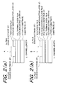
- the metal mask was replaced, an Au film having the thickness of 50nm as the source electrode 20 and the drain electrode 22 was formed on the surface of the pentacene film vacuum-deposited as described above, and thus a three organic thin film transistor according to prior art (refer to Fig.2(a) ) and three organic thin film transistors by the present invention (refer to Fig.2(b) ) were fabricated.
- the three organic thin film transistors by prior art (refer to Fig.2(a) ) and the three organic thin film transistors by the present invention (refer to Fig.2(b) ) were severally formed such that the channel length L becomes 200 ⁇ m (refer to Fig.3(a) ), 100 ⁇ m (refer to Fig.3(b) ) and 50 ⁇ m( Fig.3(c) ) as shown in Figs.3(a) (b) (c) in arrow A of Fig.2 (a) or in arrow B of Fig.2(b) . It is to be noted that a channel width W was set to 1mm for all cases.
- the three organic thin film transistor by prior art having the channel length L of 200 ⁇ m, 100 ⁇ m or 50 ⁇ m, and similarly, the three organic thin film transistor by the present invention having the channel length L of 200 ⁇ m, 100 ⁇ m or 50 ⁇ m were obtained. It is to be noted that the degree of vacuum during deposition is 2 ⁇ 10 -4 Pa for all cases in the above-described manufacturing method.
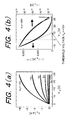
- Fig.4(a) is the graph showing the measurement result of the output characteristics of the transistor
- Fig.4(b) is the graph showing the measurement result of the transfer characteristics of the transistor.
- I D denotes a drain current
- V D denotes a drain voltage
- V G denotes a gate voltage
- V th denotes a threshold voltage in Figs.2 and 3 , and the same applies to each graph to be described below.
- the measurement result took the threshold voltage V th of +10V and the threshold voltage V th of a positive value as shown in Fig.4(b) .
- a current flows even if the gate voltage is not applied, which means that Off is not taken when the gate voltage was zero.
- the mobility of transistor is 0.069cm 2 /Vs and the on/off ratio is 6.4 ⁇ 10 3 .
- the organic thin film transistor by prior art having the channel length L of 50 ⁇ m, as shown in the graph of Fig.5 where 10 times of measurement were recorded, measurement values shifted from left to right on the graph as measurement was repeated, and operation was unstable due to the change of the measurement value changed as measurement was repeated. It is to be noted that 45 seconds were required for one measurement.
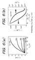
- Figs.6(a) (b) show the measurement result of the output characteristics and the transfer characteristics of the transistor by using the organic thin film transistor by the present invention having the channel length L of 50 ⁇ m (refer to Fig.2(b) and Fig.3(c) ).
- Fig.6(a) is the graph showing the measurement result of the output characteristics of the transistor
- Fig.6(b) is the graph showing the measurement result of the transfer characteristics of the transistor, where the measurement result took the threshold voltage V th of -12V and the threshold voltage V th of a negative value as shown in Fig.6 (b) .
- a current did not flow unless the gate voltage was applied, and Off was taken when the gate voltage was zero.
- the mobility of transistor is 0.17cm 2 /Vs and the on/off ratio is 8.9 ⁇ 10 4 .
- the organic thin film transistor by the present invention having the channel length L of 50 ⁇ m, as shown in the graph of Fig.7 where 10 times of measurement were recorded, measurement values are substantially overlapped with each other even if measurement was repeated, the measurement values scarcely changed even if measurement was repeated, and showed stable operation. It is to be noted that 45 seconds were required for one measurement.
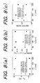
- Figs.8(a) (b) (c) show the measurement result, where Fig.8(a) is the graph showing the channel length dependency of the threshold voltage V th , Fig.8(b) is the graph showing the channel length dependency of the mobility, Fig. 8 (c) is the graph showing the channel length dependency of the on/off ratio. As shown in the graphs of Figs.
- the organic thin film transistor by the present invention shows significant improvement comparing to the organic thin film transistor by prior art in the threshold voltage V th , the mobility and the on/off ratio.
- Fig.9 shows the explanatory view of the state where the polyparaxylylene film having the thickness of 10nm formed of "dix-C” (trademark), which was formed on the surface of the SiO 2 thermal oxide film, was observed by the atomic force microscope (AFM).
- the present invention can be applied to a transistor having the shape described below, which is proposed by the present applicant.
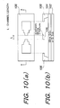
- the present applicant proposes the organic thin film transistor using the suspended bridge structure and the method for manufacturing the transistor that will be described referring to Fig.10 to Fig.12 as Patent Application 2005-27034 (filing date: February 2, 2005 ) "Method for manufacturing top-contact type field-effect transistor and top-contact type field-effect transistor".
- a solid suspended bridge structure formed of a three-layered structure by resist 106 is formed on an n-type Si substrate 102 (corresponding to the substrate 12) where an SiO 2 oxide film 104 (corresponding to the gate insulating layer 14) having the thickness of 50nm is formed on one surface as the gate insulating layer by using electron beam lithography technology (refer to Figs. 10 (a) (b) ).
- the transfer characteristics of the transistor was measured by using the organic thin film transistor including the structure shown in Fig.11(c) and the organic thin film transistor including the structure by the present invention shown in Fig.13(c) .
- the channel length of the organic thin film transistor including the structure shown in Fig.11(c) was 0.4 ⁇ m, and its channel width was 3 ⁇ m.
- the channel length of the organic thin film transistor including the structure by the present invention shown in Fig. 13 (c) is 0.35 ⁇ m, its channel width is 2.9 ⁇ m, and the thickness of "dix-C" (trademark) being the polyparaxylylene film 16 is 10nm as described above.
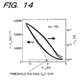
- Fig.14 is the graph showing the measurement result of the transfer characteristics of the organic thin film transistor including the structure shown in Fig.11(c) , where the threshold voltage V th was -0.3V, the mobility of transistor was 0.029cm 2 /Vs, and the on/off ratio was 2.5 ⁇ 10 2 .
- Fig.15 is the graph showing the measurement result of the transfer characteristics of the organic thin film transistor including the structure by the present invention shown in Fig.13(c) , where the threshold voltage V th is -5.6V, the mobility of transistor is 0.044cm 2 /Vs, and the on/off ratio is 4.8 ⁇ 10 3 , and the characteristics have been improved comparing to organic thin film transistor including the structure shown in Fig.11(c) .
- the water contact angle measurement method is a measurement method where one water droplet is dropped on a substrate and a contact angle of water edge with the substrate is measured.
- measurement was also performed for the SiO 2 oxide film formed on the Si substrate and HMDS coated on the surface of the SiO 2 oxide film that was formed on the Si substrate by spin coating.
- Fig.16 (a) shows the explanatory view showing the state where the SiO 2 oxide film was observed by the atomic force microscope
- Fig.16 (b) shows the explanatory view showing the state of observing the state where one water droplet was dropped on the SiO 2 oxide film by the microscope.
- the root-mean-square roughness (RMS) of the SiO 2 film was 0.1580nm, and the water contact angle was 6.8 degrees.
- Fig.17(a) shows the explanatory view showing the state where the HMDS was observed by the atomic force microscope
- Fig.17(b) shows the explanatory view showing the state of observing the state where the state where one water droplet was dropped on the HMDS by the microscope.
- Fig.18(a) shows the explanatory view showing the state of observing the state where one water droplet was dropped on "dix-C” (trademark) having the thickness of 10nm, which was formed on the SiO 2 oxide film, by the microscope
- Fig.18(b) shows the explanatory view showing the state of observing the state where one water droplet was dropped on "dix-C” (trademark) having the thickness of 415nm, which was formed on the SiO 2 oxide film, by the microscope.
- the water contact angle was 87 degrees for the both cases of film thickness 10nm and 415nm. Specifically, the water contact angle does not change even if the film thickness of "dix-C” (trademark) is made thin or thick.
- the water contact angle needs to be larger in order to modify the surface of the gate insulating layer 14 into hydrophobic, the water contact angle does not change even if the film thickness of "dix-C” (trademark) is made thin or thick, and the water contact angle of 85 degrees or larger is obtained even with the film thickness of about 5nm if the polyparaxylylene film 16 is a continuous film, and the surface of the gate insulating layer 14 is modified into hydrophobic.
- the present invention can be used in manufacturing a flexible display, a fine organic electronic device, a nano-bio device and the like which are used in electronic equipment, medical equipment and the like.
Landscapes
- Chemical & Material Sciences (AREA)
- Inorganic Chemistry (AREA)
- Engineering & Computer Science (AREA)
- Manufacturing & Machinery (AREA)
- Thin Film Transistor (AREA)
Abstract
Description
- The present invention relates to an organic thin film transistor and a method for surface modification of a gate insulating layer in the organic thin film transistor.
- Generally, there is known an organic thin film transistor using an organic substance as a material, and such an organic thin film transistor uses an oxide, for example, as a gate insulating layer.
Then, in the organic thin film transistor using an oxide as the gate insulating layer, various methods of performing surface modification of the gate insulating layer formed of an oxide have been proposed to improve its transistor characteristics.
Conventionally, as a method of performing surface modification of the gate insulating layer formed of the oxide, a method of forming a self-assembled film such as octadecyltrichlorosilane (OTS) and 1,1,1,3,3,3-hexamethyldisilazane (HMDS), for example, has been mentioned. Meanwhile, refer toNon-patent Documents 1 to 4 for the method concerning OTS, and refer toNon-patent Document 5 for the method concerning HMDS. - However, the above-described conventional method was limited to the case where the gate insulating layer is formed of an oxide, had a problems that it could not be applied to the case where the gate insulating layer was formed of a substance other than the oxide.
- Further, as a patent document related to the organic thin film transistor, there is Japanese Patent Laid-open No.
2003-255857 Patent Document 1, for example. - Non-patent Document 1 : D.J.Gundlach, J.A.Nichols, L.Zhou and T.N.Jackson, Appl.Phys.Lett.80, 2925(2002)
Non-patent Document 2 : M.Shtein, J.Mapel, J.B.Benziger and S.Forrest, Appl.Phys.Lett.81, 263(2002)
Non-patent Document 3 : D.Knipp, R.A.Street, A.Volkel and J.Ho, J.Appl.Phys.93, 347(2003)
Non-patent Document 4 : J.Lee, K. Kim, J.H.Kim, S. Im and D. Jung, Appl.Phys.Lett.82, 4169(2003)
Non-patent Document 5 : I.Yagi, K.Tsukagoshi, Y.Aoagi, Appl.Phys.Lett.86, 103502(2005)
Patent Document 1 : Japanese Patent Laid-open No.2003-255857 - The present invention has been created in view of the above-described problem that prior art has, and it is an object of the invention to provide an organic thin film transistor and a method for surface modification of the gate insulating layer of the organic thin film transistor, which is capable of modifying the surface of the gate insulating layer not only in the case where the gate insulating layer is formed of an oxide but also in the case where the gate insulating layer is formed of a substance other than the oxide, and consequently transistor characteristics can be significantly improved.
- To achieve the above-described objects, the present invention is designed that a layer formed of polyparaxylylene (poly para-xylylene) is formed on the surface of the gate insulating layer.
The formation of polyparaxylylene layer on the surface of the gate insulating layer should only be performed by depositing polyparaxylylene film on the surface of the gate insulating layer by using a chemical vapor deposition (CVD), for example.
Herein, it is preferable that polyparaxylylene have high purity, that is, the purity of 99% or higher, and polychloroparaxylylene whose purity exceeds 99% can be used, for example.
According to the present invention, by the polyparaxylylene layer that is formed on the surface of the gate insulating layer formed of an oxide or a substance other than the oxide, the surface of the gate insulating layer is modified to hydrophobic, a threshold voltage becomes negative, Off can be taken when a gate voltage is zero, and stable operation can be obtained as a transistor. - Specifically, the present invention is an organic thin film transistor where an organic semiconductor layer is stacked on a gate insulating layer and an electrode is formed on the organic semiconductor layer, in which a polyparaxylylene layer formed of a continuous polyparaxylylene film is formed on the surface of the gate insulating layer, between the gate insulating layer and the organic semiconductor layer, so as to face and contact the organic semiconductor layer.
Further, the present invention, in the above-described invention is designed that the polyparaxylylene film is a continuous film whose film thickness shows the angle of 85 degrees or more by contact angle measurement of water.
Further, the present invention, in the above-described invention is designed that the polyparaxylylene has the purity of 99% or higher.
Further, the present invention, in the above-described invention is designed that the thickness of the polyparaxylylene film is 5 to 200nm.
Further, the present invention, in the above-described invention is designed that the polyparaxylylene is polychloroparaxylylene.
Further, the present invention, in the method for surface modification of the gate insulating layer in the organic thin film transistor where the organic semiconductor layer is stacked on the gate insulating layer and the electrode is formed on the organic semiconductor layer is designed that the polyparaxylylene film is deposited on the surface of the gate insulating layer as continuous film having a predetermined thickness by chemical vapor deposition.
Further, the present invention, in the above-described invention is designed that the film thickness of the continuous film shows the angle of 85 degrees or more by the contact angle evaluation of water.
Further, the present invention, in the above-described invention is designed that the polyparaxylylene has the purity of 99% or higher.
Further, the present invention, in the above-described invention is designed that the film thickness of the continuous film is 5 to 200nm.
Further, the present invention, the above-described invention is designed that the polyparaxylylene is polychloroparaxylylene. - Since the present invention is constituted as described above, the invention exerts an excellent effect that it can perform modification of the surface of the gate insulating layer not only in the case where the gate insulating layer is formed of an oxide but also in the case where the gate insulating layer is formed of a substance other than the oxide, and consequently transistor characteristics can be significantly improved.
- [
Figure 1] Fig.1 is a constitution explanatory view showing an example of an embodiment of the organic thin film transistor according to the present invention. - [
Figure2] Figs.2(a)(b) respectively show an organic thin film transistor by prior art and the organic thin film transistor by the present invention, in whichFig.2(a) is a constitution explanatory view of the organic thin film transistor by prior art, andFig.2(b) is a constitution explanatory view of the organic thin film transistor by the present invention. - [
Figure 3] Figs.3(a) (b) (c) are explanatory views showing the state where the film observed by an optical microscope in arrow A ofFig.2 (a) and in arrow B ofFig.2(b) , whereFig. 3 (a) shows the case where a channel length L is 200µm,Fig. 3 (b) shows the case where the channel length L is 100µm, andFig.3 (c) shows the case where the channel length L is 50µm. - [
Figure 4] Figs.4(a) (b) are graphs showing experiment results by the present inventor using the organic thin film transistor having the channel length L of 50µm by prior art, whereFig. 4 (a) is a graph showing the measurement result of the output characteristics of the transistor andFig.4 (b) is a graph showing the measurement result of the transfer characteristics of the transistor. - [
Figure 5] Fig.5 is a graph showing an experiment result by the present inventor using the organic thin film transistor having the channel length L of 50µm by prior art, where 10 times of measurement were recorded. - [
Figure 6] Figs.6(a) (b) are graphs showing experiment results by the present inventor using the organic thin film transistor having the channel length L of 50µm by the present invention, whereFig.6(a) is a graph showing the measurement result of the output characteristics of the transistor, andFig.6(b) is a graph showing the measurement result of the transfer characteristics of the transistor. - [
Figure 7] Fig.7 is a graph showing an experiment result by the present inventor using the organic thin film transistor having the channel length L of 50µm by the present invention, where 10 times of measurement were recorded. - [
Figure 8] Figs.8(a) (b) (c) are graphs showing experiment results where the channel length dependency of a threshold voltage Vth, mobility and on/off ratio regarding the organic thin film transistor by prior art and the organic thin film transistor by the present invention each having the channel length L of 50 µm, 100 µm and 200 µm were measured, whereFig. 8 (a) is a graph showing the channel length dependency of the threshold voltage Vth,Fig.8(b) is a graph showing the channel length dependency of mobility,Fig.8(c) is a graph showing the channel length dependency of on/off ratio. - [
Figure 9] Fig. 9 is an explanatory view showing the state where a polyparaxylylene film having the thickness of 10nm formed of "dix-C" (trademark), which is formed on the surface of an SiO2 thermal oxide film, is observed by an atomic force microscope (AFM). - [
Figure 10] Figs.10(a) (b) are explanatory views of an organic thin film transistor and the method for manufacturing the transistor, which uses a suspension bridge structure shown in Patent Application2005-27034 (filing date: February 2, 2005 Fig.10(a) is a top surface explanatory view showing the state where a solid suspension bridge structure formed of a three-layered structure is formed by resist on an n-type Si substrate where the SiO2 oxide film is formed, andFig.10(b) is an end surface explanatory view when the transistor is cut off by X-X line ofFig.10(a) . - [
Figure 11] Figs.11 (a) (b) (c) are explanatory views of an organic thin film transistor and the method for manufacturing the transistor, which uses a suspension bridge structure shown in Patent Application2005-27034 (filing date: February 2, 2005 Fig.11(a) is the explanatory view of a first process,Fig.11(b) is the explanatory view of a second process, andFig.11(c) is the explanatory view of a third process. - [
Figure 12] Fig.12 is a conceptual constitution explanatory view of the organic thin film transistor using the suspension bridge structure. - [
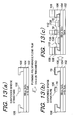
Figure 13] Figs.13(a) (b) (c) are explanatory views showing a processing when applying the present invention to the organic thin film transistor using the suspended bridge structure, whereFig.13(a) is an explanatory view showing an n-type Si substrate where resist including the suspended bridge structure is formed on the SiO2 oxide film,Fig.13(b) is an explanatory view showing the processing of forming the polyparaxylylene film, andFig.13(c) is an explanatory view showing a transistor structure that is obtained by executing the first process to the third process shown inFigs.11(a) (b) (c) . - [
Figure 14] Fig.14 is a graph showing an experiment result by the present inventor using the organic thin film transistor including the structure shown inFig.11(c) , and is a graph showing the measurement result of the transfer characteristics of the transistor including the structure shown inFig.11(c) . - [
Figure 15] Fig.15 is a graph showing an experiment result by the present inventor, which uses the organic thin film transistor including the structure by the present invention shown inFig.13(c) , and a graph showing the measurement result of the transfer characteristics of the transistor including the structure by the present invention shown inFig.11(c) . - [
Figure 16] Fig.16(a) is an explanatory view showing the state where the SiO2 oxide film was observed by the atomic force microscope,Fig. 16 (b) is an explanatory view showing the state where one water droplet was dropped on the SiO2 oxide film was observed by a microscope. - [
Figure 17] Fig.17(a) is an explanatory view showing the state where HMDS is observed by the atomic force microscope, andFig.17(b) is an explanatory view showing the state of observing the state where one water droplet was dropped on HMDS by the microscope. - [
Figure 18] Fig.18(a) is an explanatory view showing the state of observing the state where one water droplet was dropped on a "dix-C" (trademark) having the thickness of 10nm formed on the SiO2 oxide film, andFig.18(b) is an explanatory view showing the state of observing the state where one water droplet was dropped on the "dix-C" (trademark) having the thickness of 415nm formed on the SiO2 oxide film. -
- 10
- Organic thin film transistor
- 12
- Substrate
- 12a
- Surface
- 14
- Gate insulating layer
- 14a
- Surface
- 16
- Polyparaxylylene film
- 16a
- Surface
- 18
- Organic semiconductor layer
- 18a
- Surface
- 20
- Source electrode
- 22
- Drain electrode
- 100
- Organic thin film transistor
- 102
- n-type Si substrate
- 104
- SiO2 oxide film
- 106
- Resist
- 108
- Pentacene film
- 110
- Source electrode
- 112
- Drain electrode
- Hereinafter, description will be made in detail for an example of the embodiments of the organic thin film transistor and the method for surface modification of the gate insulating layer in the organic thin film transistor according to the present invention by referring to the attached drawings.
-
Fig.1 shows the constitution explanatory view of an example of the embodiment of the organic thin film transistor according to the present invention.
Specifically, an organicthin film transistor 10 according to an example of the present invention is constituted by having: asubstrate 12 formed of semiconductor, which is a gate layer that functions as a substrate and a gate electrode; agate insulating layer 14 formed of an insulative material, which is formed on onesurface 12a of thesubstrate 12; apolyparaxylylene film 16 being a polyparaxylylene layer, which is formed on thesurface 14a of thegate insulating layer 14 by depositing polyparaxylylene; anorganic semiconductor layer 18 being an active layer formed of an organic material, which is formed on the surface 16a of thepolyparaxylylene film 16; asource electrode 20 being a first electrode formed of a conductive material, which is formed on thesurface 18a of theorganic semiconductor layer 18; and adrain electrode 22 being a second electrode formed of a conductive material, which is formed on thesurface 18a of theorganic semiconductor layer 18.
Specifically, in the organicthin film transistor 10, thepolyparaxylylene film 16 and theorganic semiconductor layer 18 face and contact with each other, and thepolyparaxylylene film 16 is arranged directly under theorganic semiconductor layer 18.
It is to be noted that thepolyparaxylylene film 16 and theorganic semiconductor layer 18 should only be formed by deposition, for example.
Herein, as thesubstrate 12, an n-type Si substrate being an Si substrate doped with phosphorus can be used, for example, but the substrate is not limited to this, and an n-type semiconductor substrate or a p-type semiconductor substrate where various impurities are doped in various semiconductor materials can be used.
Further, as thegate insulating layer 14, an SiO2 film being an insulative material can be used, for example, but the layer is not limited to this, and polymer film such as polyvinylphenol (PVP), polyvinylalcohol (PVA) and polystyrene (PS), for example, can be used instead of an oxide like SiO2.
Moreover, thepolyparaxylylene film 16 is formed as a continuous film, that is, a continuous film having no holes formed therein, and it is preferable to form the film by high-purity polyparaxylylene, for example, more particularly polyparaxylylene whose purity is 99% or higher. Further, although the film thickness of the polyparaxylylene film is not particularly limited, it is preferable that the thickness be about 5 to 200nm, more particularly about 5 to 100nm. Particularly, in the case where the surface of thepolyparaxylylene film 16 can be formed homogeneously, the film thickness can be made as thin as about 5nm, for example.
It is to be noted that formation of a film whose surface is homogeneous is made possible by using high-purity polyparaxylylene.
Furthermore, as an organic material for forming theorganic semiconductor layer 18, pentacene (Pentacene) can be used for example, but the material is not limited to this, and various organic materials such as copper phthalocyanine and thiophenes can be used, for example.
Further, thesource electrode 20 and thedrain electrode 22 can be formed by depositing metal being a conductive material which is Au, for example, by vapor deposition on thesurface 18a of theorganic semiconductor layer 18, for example, an Au electrode formed in this manner can be used as thesource electrode 20 and thedrain electrode 22. It is to be noted that a conductive material used as thesource electrode 20 and thedrain electrode 22 is not limited to Au, but Pt, Ag or the like can be used. - In the constitution above, in the above-described organic
thin film transistor 10, thepolyparaxylylene film 16 modifies the surface of thegate insulating layer 14 from hydrophilic to hydrophobic, and consequently, the transistor characteristics of the organicthin film transistor 10 could be significantly improved. - Next, description will be made for the experiment and its result by the present inventor, the organic thin film transistor by prior art and the organic thin film transistor by the present invention were fabricated in this experiment, and the transistor characteristics of the both transistors were compared.
First, description will be made for the manufacturing methods of the organic thin film transistor by prior art and the organic thin film transistor by the present invention used in the experiment. As thesubstrate gate insulating layer 14 was formed on one surface were prepared and oxygen plasma cleaning was performed after solution cleaning by acetone and isopropyl alcohol was performed.
Regarding 3 pieces of n-type Si substrate out of the 6 pieces of the n-type Si substrate to which the above-described processing was performed, only on the surface of their SiO2 thermal oxide film, a film formed of high-purity polychloroparaxylylene (poly chloro-para-xylylene) having the purity of 99% or higher was deposited as thepolyparaxylylene film 16 by chemical vapor deposition (CVD) to so to be formed in the thickness of 10nm.
Meanwhile, in this experiment, "dix-C" (trademark) that is one of polyparaxylylene, which is generally called as "diX" (trademark) manufactured by Daisan Kasei Co., Ltd., was used as the high-purity polychloroparaxylylene having the purity of 99% or higher. It is to be noted that "diX" (trademark) has purity exceeding 99%.
Further, to deposit "dix-C" (trademark) on the surface of the SiO2 thermal oxide film by chemical vapor deposition in this experiment, it was performed under reduced pressure by using an exclusive unit called "DACS-0" (trademark) manufactured by KISCO Ltd., which is used for coating "diX" (trademark) manufactured by Daisan Kasei Co., Ltd. This unit mainly consists of the 3 portions of a vaporizer, a pyrolizer and a deposition chamber, where the n-type Si substrate on which the SiO2 thermal oxide film is formed is arranged in the deposition chamber, and powder of "dix-C" (trademark) being the coating material is arranged in the vaporizer. Then, after decompressing inside the unit, the temperature of the vaporizer is increased (120 to 180°C) to evaporate "dix-C"(trademark). When the evaporated gas is drawn by a vacuum pump to flow toward the deposition chamber side, and passes through the high-temperature (650 to 700°C) pyrolizer, the gas is thermally decomposed into monomer. Moreover, when the monomer contacts the SiO2 thermal oxide film inside the deposition chamber of room temperature, it is cooled down and polymerized on the surface, and a high-molecular weight polyparaxylylene film is formed on the surface of the SiO2 thermal oxide film.
Then, on the above-described 6 pieces of n-type Si substrates, pentacene film having the thickness of 30nm was vacuum-deposited as theorganic semiconductor layer 18 through a metal mask.
Next, the metal mask was replaced, an Au film having the thickness of 50nm as thesource electrode 20 and thedrain electrode 22 was formed on the surface of the pentacene film vacuum-deposited as described above, and thus a three organic thin film transistor according to prior art (refer toFig.2(a) ) and three organic thin film transistors by the present invention (refer toFig.2(b) ) were fabricated.
Herein, the three organic thin film transistors by prior art (refer toFig.2(a) ) and the three organic thin film transistors by the present invention (refer toFig.2(b) ) were severally formed such that the channel length L becomes 200 µm (refer toFig.3(a) ), 100µm (refer toFig.3(b) ) and 50µ m(Fig.3(c) ) as shown inFigs.3(a) (b) (c) in arrow A ofFig.2 (a) or in arrow B ofFig.2(b) . It is to be noted that a channel width W was set to 1mm for all cases.
Therefore, according to the above-described manufacturing method, the three organic thin film transistor by prior art having the channel length L of 200 µm, 100 µm or 50 µm, and similarly, the three organic thin film transistor by the present invention having the channel length L of 200µm, 100µm or 50 µm were obtained.
It is to be noted that the degree of vacuum during deposition is 2×10⁻⁴Pa for all cases in the above-described manufacturing method. - First, the output characteristics and the transfer characteristics of the transistor were measured by using the organic thin film transistor by prior art having the channel length L of 50µm (refer to
Fig.2(a) andFig.3(c) ).
Herein,Fig.4(a) is the graph showing the measurement result of the output characteristics of the transistor, andFig.4(b) is the graph showing the measurement result of the transfer characteristics of the transistor. It is to be noted that ID denotes a drain current, VD denotes a drain voltage, VG denotes a gate voltage, Vth denotes a threshold voltage inFigs.2 and3 , and the same applies to each graph to be described below.
The measurement result took the threshold voltage Vth of +10V and the threshold voltage Vth of a positive value as shown inFig.4(b) . Specifically, a current flows even if the gate voltage is not applied, which means that Off is not taken when the gate voltage was zero.
It is to be noted that the mobility of transistor is 0.069cm2/Vs and the on/off ratio is 6.4×10³.
Further, in the organic thin film transistor by prior art having the channel length L of 50 µm, as shown in the graph ofFig.5 where 10 times of measurement were recorded, measurement values shifted from left to right on the graph as measurement was repeated, and operation was unstable due to the change of the measurement value changed as measurement was repeated. It is to be noted that 45 seconds were required for one measurement. - On the other hand,
Figs.6(a) (b) show the measurement result of the output characteristics and the transfer characteristics of the transistor by using the organic thin film transistor by the present invention having the channel length L of 50µm (refer toFig.2(b) andFig.3(c) ).
Herein,Fig.6(a) is the graph showing the measurement result of the output characteristics of the transistor andFig.6(b) is the graph showing the measurement result of the transfer characteristics of the transistor, where the measurement result took the threshold voltage Vth of -12V and the threshold voltage Vth of a negative value as shown inFig.6 (b) . Specifically, a current did not flow unless the gate voltage was applied, and Off was taken when the gate voltage was zero.
It is to be noted that the mobility of transistor is 0.17cm2/Vs and the on/off ratio is 8.9×10⁴.
Further, in the organic thin film transistor by the present invention having the channel length L of 50 µm, as shown in the graph ofFig.7 where 10 times of measurement were recorded, measurement values are substantially overlapped with each other even if measurement was repeated, the measurement values scarcely changed even if measurement was repeated, and showed stable operation. It is to be noted that 45 seconds were required for one measurement. - Next, by using the organic thin film transistor by prior art and the organic thin film transistor by the present invention each having the channel length L of 50µm, 100µm and 200µm, each channel length dependency for the threshold voltage Vth, the mobility and the on/off ratio was measured.
Figs.8(a) (b) (c) show the measurement result, whereFig.8(a) is the graph showing the channel length dependency of the threshold voltage Vth,Fig.8(b) is the graph showing the channel length dependency of the mobility,Fig. 8 (c) is the graph showing the channel length dependency of the on/off ratio.
As shown in the graphs ofFigs. 8 (a) (b) (c) , in all channel lengths having the channel length L of 50µm, 100µm and 200 µm, the organic thin film transistor by the present invention shows significant improvement comparing to the organic thin film transistor by prior art in the threshold voltage Vth, the mobility and the on/off ratio. - Herein,
Fig.9 shows the explanatory view of the state where the polyparaxylylene film having the thickness of 10nm formed of "dix-C" (trademark), which was formed on the surface of the SiO2 thermal oxide film, was observed by the atomic force microscope (AFM).
The polyparaxylylene film having the thickness of 10nm formed of "dix-C" (trademark) has:
Average roughness (Ra)=0.4847nm;
Maximum vertical interval (P-V)=4.76nm; and
Root-mean-square roughness (RMS)=0.6093nm and includes a relatively flat surface shape.
Meanwhile, for reference, the SiO2 thermal oxide film formed on the n-type Si substrate had Root-mean-square roughness (RMS)=0.158nm. - Further, since the polyparaxylylene film has characteristics that it thoroughly grows around the surface of an object, the present invention can be applied to a transistor having the shape described below, which is proposed by the present applicant.
Specifically, the present applicant proposes the organic thin film transistor using the suspended bridge structure and the method for manufacturing the transistor that will be described referring toFig.10 to Fig.12 as Patent Application2005-27034 (filing date: February 2, 2005
To fabricate the organic thin film transistor using the suspension bridge structure, firstly, a solid suspended bridge structure formed of a three-layered structure by resist 106 is formed on an n-type Si substrate 102 (corresponding to the substrate 12) where an SiO2 oxide film 104 (corresponding to the gate insulating layer 14) having the thickness of 50nm is formed on one surface as the gate insulating layer by using electron beam lithography technology (refer toFigs. 10 (a) (b) ).
Then, to the n-type Si substrate 102 where the resist 106 including the suspended bridge structure was formed on the SiO2 oxide film 104, by performing a first process of depositing a pentacene film 108 (corresponding to the organic semiconductor layer 18) at the deposition angle of 45 degrees to a vertical direction (refer toFig.11(a) ), a second process of depositing the pentacene film 108 (corresponding to the organic semiconductor layer 18) at the deposition angle of 45 degrees to the vertical direction which is symmetrical to the deposition angle in the first process (refer toFig.11(b) ), and a third process of depositing a metal material, which becomes a source electrode 110 (corresponding to the source electrode 20) and a drain electrode 112 (corresponding to the drain electrode 22), from the vertical direction (refer toFig.11(c) ), an organicthin film transistor 100 using the suspended bridge structure as conceptually shown inFig.12 can be formed.
It is to be noted that a channel is formed under the suspended bridge structure in such an organic thin film transistor using the suspended bridge structure. - Herein, in applying the present invention to the above-described organic thin film transistor using the suspended bridge structure, as shown in
Figs.13(a) (b) (c) , to the n-type Si substrate 102 where the resist 106 including the suspended bridge structure is formed on the SiO2 oxide film 104 having the thickness of 50nm (refer toFig.13(a) ), "dix-C" (trademark) being the high-purity polychloroparaxylylene exceeding the purity of 99% is formed as thepolyparaxylylene film 16 in the thickness of 10nm by chemical vapor deposition (refer toFig.13(b) ). Since the polyparaxylylene film has characteristics that it thoroughly grows around the surface of an object, the film also thoroughly grows under the suspended bridge structure.
Then, the first process to the third process shown inFigs.11(a) (b) (c) described above are executed to form the transistor structure (refer toFig.13(c) ). - Next, the transfer characteristics of the transistor was measured by using the organic thin film transistor including the structure shown in
Fig.11(c) and the organic thin film transistor including the structure by the present invention shown inFig.13(c) . It is to be noted that the channel length of the organic thin film transistor including the structure shown inFig.11(c) was 0.4µm, and its channel width was 3µ m. On the other hand, the channel length of the organic thin film transistor including the structure by the present invention shown inFig. 13 (c) is 0.35µm, its channel width is 2.9µm, and the thickness of "dix-C" (trademark) being thepolyparaxylylene film 16 is 10nm as described above.
Fig.14 is the graph showing the measurement result of the transfer characteristics of the organic thin film transistor including the structure shown inFig.11(c) , where the threshold voltage Vth was -0.3V, the mobility of transistor was 0.029cm2/Vs, and the on/off ratio was 2.5×10².
On the other hand,Fig.15 is the graph showing the measurement result of the transfer characteristics of the organic thin film transistor including the structure by the present invention shown inFig.13(c) , where the threshold voltage Vth is -5.6V, the mobility of transistor is 0.044cm2/Vs, and the on/off ratio is 4.8×10³, and the characteristics have been improved comparing to organic thin film transistor including the structure shown inFig.11(c) . - Herein, description will be made for a measurement result by a contact angle measurement method for evaluating water contact angle where the water contact angle of "dix-C" (trademark) the
polyparaxylylene film 16 was measured.
It is to be noted that the water contact angle measurement method is a measurement method where one water droplet is dropped on a substrate and a contact angle of water edge with the substrate is measured.
Herein, for comparison, measurement was also performed for the SiO2 oxide film formed on the Si substrate and HMDS coated on the surface of the SiO2 oxide film that was formed on the Si substrate by spin coating.
Fig.16 (a) shows the explanatory view showing the state where the SiO2 oxide film was observed by the atomic force microscope, andFig.16 (b) shows the explanatory view showing the state of observing the state where one water droplet was dropped on the SiO2 oxide film by the microscope.
The root-mean-square roughness (RMS) of the SiO2 film was 0.1580nm, and the water contact angle was 6.8 degrees.
Further,Fig.17(a) shows the explanatory view showing the state where the HMDS was observed by the atomic force microscope, andFig.17(b) shows the explanatory view showing the state of observing the state where the state where one water droplet was dropped on the HMDS by the microscope.
The root-mean-square roughness (RMS) of the HMDS was 0.1638nm, and the water contact angle was 70 degrees.
Then,Fig.18(a) shows the explanatory view showing the state of observing the state where one water droplet was dropped on "dix-C" (trademark) having the thickness of 10nm, which was formed on the SiO2 oxide film, by the microscope, andFig.18(b) shows the explanatory view showing the state of observing the state where one water droplet was dropped on "dix-C" (trademark) having the thickness of 415nm, which was formed on the SiO2 oxide film, by the microscope.
Regarding "dix-C" (trademark), the water contact angle was 87 degrees for the both cases of film thickness 10nm and 415nm. Specifically, the water contact angle does not change even if the film thickness of "dix-C" (trademark) is made thin or thick.
Herein, although the water contact angle needs to be larger in order to modify the surface of thegate insulating layer 14 into hydrophobic, the water contact angle does not change even if the film thickness of "dix-C" (trademark) is made thin or thick, and the water contact angle of 85 degrees or larger is obtained even with the film thickness of about 5nm if thepolyparaxylylene film 16 is a continuous film, and the surface of thegate insulating layer 14 is modified into hydrophobic. - It is to be noted that the above-described embodiment may be modified as described in (1) to (3) below.
- (1) In the above-described embodiment, polychloroparaxylylene whose purity exceeds 99% was shown as an example of polyparaxylylene, it goes out without saying that the material is not limited to this, and polyparaxylylene derivative using 4-amino (2,2) paracyclophane, 4-aminomethyl (2,2) paracyclophane, tetrachloro (2,2) paracyclophane, 1,1,9,9-tetrafluoro (2,2) paracyclophane or the like as an initial material can be used.
- (2) In the above-described embodiment, specific material names and thickness have been shown regarding the
substrate 12, thegate insulating layer 14, theorganic semiconductor layer 18, thesource electrode 20 and thedrain electrode 22, but it goes without saying that the materials and the thickness are merely examples, and it is a matter of course that materials and the thickness may be appropriately selected corresponding to design conditions or the like. - (3) The modification examples shown in the above-described embodiment and above-described (1) to (2) may be appropriately combined.
- The present invention can be used in manufacturing a flexible display, a fine organic electronic device, a nano-bio device and the like which are used in electronic equipment, medical equipment and the like.
Claims (10)
- An organic thin film transistor where an organic semiconductor layer is stacked on a gate insulating layer and an electrode is formed on said organic semiconductor layer, wherein
a polyparaxylylene layer formed of continuous polyparaxylylene film is formed on the surface of said gate insulating layer, between the gate insulating layer and the organic semiconductor layer, so as to face and contact said organic semiconductor layer. - The organic thin film transistor according to Claim 1, wherein
said polyparaxylylene film is a continuous film whose film thickness shows the angle of 85 degrees or more by contact angle measurement of water. - The organic thin film transistor according to any one of Claims 1 and 2, wherein
said polyparaxylylene has the purity of 99% or higher. - The organic thin film transistor according to any one of Claims 1, 2 and 3, wherein
the thickness of said polyparaxylylene film is 5 to 200nm. - The organic thin film transistor according to any one of Claims 1, 2, 3 and 4 wherein
said polyparaxylylene is polychloroparaxylylene. - A method for surface modification of a gate insulating layer in an organic thin film transistor where an organic semiconductor layer is stacked on a gate insulating layer and an electrode is formed on said organic semiconductor layer, wherein
a polyparaxylylene film is deposited as a continuous film having a predetermined thickness on the surface of the gate insulating layer by chemical vapor deposition. - The method for surface modification of a gate insulating layer in an organic thin film transistor according to Claim 6, wherein
the film thickness of said continuous film shows the angle of 85 degrees or more by contact angle evaluation of water. - The method for surface modification of a gate insulating layer in an organic thin film transistor according to any one of Claims 6 and 7, wherein
said polyparaxylylene has the purity of 99% or higher. - The method for surface modification of a gate insulating layer in an organic thin film transistor according to any one of Claims 6, 7 and 8, wherein
the film thickness of said continuous film is 5 to 200nm. - The method for surface modification of a gate insulating layer in an organic thin film transistor according to any one of Claims 6, 7, 8 and 9, wherein
said polyparaxylylene is polychloroparaxylylene.
Applications Claiming Priority (2)
| Application Number | Priority Date | Filing Date | Title |
|---|---|---|---|
| JP2005252256 | 2005-08-31 | ||
| PCT/JP2006/316687 WO2007026608A1 (en) | 2005-08-31 | 2006-08-25 | Organic thin film transistor, and method for surface modification of gate insulating layer in organic thin film transistor |
Publications (1)
| Publication Number | Publication Date |
|---|---|
| EP1930940A1 true EP1930940A1 (en) | 2008-06-11 |
Family
ID=37808702
Family Applications (1)
| Application Number | Title | Priority Date | Filing Date |
|---|---|---|---|
| EP06783033A Withdrawn EP1930940A1 (en) | 2005-08-31 | 2006-08-25 | Organic thin film transistor, and method for surface modification of gate insulating layer in organic thin film transistor |
Country Status (4)
| Country | Link |
|---|---|
| US (1) | US20080315190A1 (en) |
| EP (1) | EP1930940A1 (en) |
| JP (1) | JPWO2007026608A1 (en) |
| WO (1) | WO2007026608A1 (en) |
Families Citing this family (4)
| Publication number | Priority date | Publication date | Assignee | Title |
|---|---|---|---|---|
| JPWO2008155930A1 (en) * | 2007-06-20 | 2010-08-26 | 日本電気株式会社 | Switching element |
| JP5636626B2 (en) * | 2007-12-27 | 2014-12-10 | ソニー株式会社 | Method for forming semiconductor thin film and method for manufacturing thin film semiconductor device |
| JP5943590B2 (en) | 2011-01-07 | 2016-07-05 | 日本発條株式会社 | Piezoelectric element manufacturing method, piezoelectric element, piezoelectric actuator, and head suspension |
| US10388895B2 (en) * | 2017-11-07 | 2019-08-20 | Shenzhen China Star Optoelectonics Semiconductor Display Technology Co., Ltd. | Organic thin film transistor with charge injection layer and manufacturing method thereof |
Family Cites Families (3)
| Publication number | Priority date | Publication date | Assignee | Title |
|---|---|---|---|---|
| US7166689B2 (en) * | 2003-02-13 | 2007-01-23 | Ricoh Company, Ltd. | Aryl amine polymer, thin film transistor using the aryl amine polymer, and method of manufacturing the thin film transistor |
| JP4480410B2 (en) * | 2003-10-31 | 2010-06-16 | 株式会社リコー | Organic semiconductor material, organic thin film transistor, and manufacturing method thereof |
| JP2006173532A (en) * | 2004-12-20 | 2006-06-29 | Nippon Hoso Kyokai <Nhk> | Organic transistor and method for forming organic transistor |
-
2006
- 2006-08-25 US US12/065,416 patent/US20080315190A1/en not_active Abandoned
- 2006-08-25 EP EP06783033A patent/EP1930940A1/en not_active Withdrawn
- 2006-08-25 JP JP2007533210A patent/JPWO2007026608A1/en active Pending
- 2006-08-25 WO PCT/JP2006/316687 patent/WO2007026608A1/en not_active Ceased
Non-Patent Citations (1)
| Title |
|---|
| See references of WO2007026608A1 * |
Also Published As
| Publication number | Publication date |
|---|---|
| US20080315190A1 (en) | 2008-12-25 |
| WO2007026608A1 (en) | 2007-03-08 |
| JPWO2007026608A1 (en) | 2009-03-05 |
Similar Documents
| Publication | Publication Date | Title |
|---|---|---|
| US10636652B2 (en) | Method of forming a semiconductor device using layered etching and repairing of damaged portions | |
| EP1485958B1 (en) | Self-aligned nanotube field effect transistor and method of fabricating same | |
| TWI463654B (en) | Self-aligned process of nano tube/nano wire field effect transistor | |
| TWI573799B (en) | An organic semiconductor composition comprising a non-polymeric material having a polydispersity of 1, at least one solvent, and a crystal modifier, and an organic thin film transistor using the same | |
| US8642432B2 (en) | N-dopant for carbon nanotubes and graphene | |
| JP2011061046A (en) | Three-terminal type electronic device and two-terminal type electronic device | |
| US11961898B2 (en) | Method of patterning two-dimensional material layer on substrate, and method of fabricating semiconductor device | |
| Oh | Organic thin-film transistors using pentacene and SiOC film | |
| CN105895704A (en) | Graphene field effect transistor and manufacturing method thereof | |
| US7045814B2 (en) | OFET structures with both n- and p-type channels | |
| JPWO2007094164A1 (en) | Organic thin film transistor and manufacturing method thereof | |
| KR101978944B1 (en) | Transistor and preparation method thereof | |
| US20080315190A1 (en) | Organic Thin Film Transistor and Method for Surface Modification of Gate Insulating Layer of Organic Thin Film Transistor | |
| CN103890988A (en) | Organic single crystal film, organic single crystal film array, and semiconductor device including an organic single crystal film | |
| KR102845024B1 (en) | Organic semiconductor device, method for manufacturing an organic semiconductor single crystal film, and method for manufacturing an organic semiconductor device | |
| Kannan et al. | Controllable switching ratio in quantum dot/metal–metal oxide nanostructure based non-volatile memory device | |
| KR100602259B1 (en) | A vertical field-effect transistor, method for manufacturing the same, and a display device having the same | |
| Kim et al. | A direct metal transfer method for cross-bar type polymer non-volatile memory applications | |
| JP7558569B2 (en) | Graphene laminate and method for producing same | |
| Xiao et al. | Fabrication of field-effect transistors with transfer-free nanostructured carbon as the semiconducting channel material | |
| KR102639310B1 (en) | Semiconductor device including iodine-doped CuO film and manufacturing method thereof | |
| Wu et al. | Lithography‐Free Microfabrication of Electrode Arrays with 2 μm Electrode Gaps Using Topographic Templates | |
| Cha et al. | High performance ZnO nanowire field effect transistor | |
| JP5610387B2 (en) | Organic thin film semiconductor device and manufacturing method thereof | |
| Trivedi et al. | The fabrication of high density nanochannel organic light emitting diodes with reduced charge spreading |
Legal Events
| Date | Code | Title | Description |
|---|---|---|---|
| PUAI | Public reference made under article 153(3) epc to a published international application that has entered the european phase |
Free format text: ORIGINAL CODE: 0009012 |
|
| 17P | Request for examination filed |
Effective date: 20080313 |
|
| AK | Designated contracting states |
Kind code of ref document: A1 Designated state(s): AT BE BG CH CY CZ DE DK EE ES FI FR GB GR HU IE IS IT LI LT LU LV MC NL PL PT RO SE SI SK TR |
|
| RIN1 | Information on inventor provided before grant (corrected) |
Inventor name: AOYAGI, YOSHINOBU Inventor name: YAGI, IWAO Inventor name: SHIGETO, KUNJI Inventor name: TSUKAGOSHI, KAZUHITOC/O RIKEN |
|
| STAA | Information on the status of an ep patent application or granted ep patent |
Free format text: STATUS: THE APPLICATION HAS BEEN WITHDRAWN |
|
| 18W | Application withdrawn |
Effective date: 20100702 |