EP1930755A1 - Optical waveguide device and method for fabricating optical waveguide device - Google Patents
Optical waveguide device and method for fabricating optical waveguide device Download PDFInfo
- Publication number
- EP1930755A1 EP1930755A1 EP06767042A EP06767042A EP1930755A1 EP 1930755 A1 EP1930755 A1 EP 1930755A1 EP 06767042 A EP06767042 A EP 06767042A EP 06767042 A EP06767042 A EP 06767042A EP 1930755 A1 EP1930755 A1 EP 1930755A1
- Authority
- EP
- European Patent Office
- Prior art keywords
- light
- core section
- optical waveguide
- body portion
- waveguide device
- Prior art date
- Legal status (The legal status is an assumption and is not a legal conclusion. Google has not performed a legal analysis and makes no representation as to the accuracy of the status listed.)
- Withdrawn
Links
Images





Classifications
-
- G—PHYSICS
- G02—OPTICS
- G02B—OPTICAL ELEMENTS, SYSTEMS OR APPARATUS
- G02B6/00—Light guides; Structural details of arrangements comprising light guides and other optical elements, e.g. couplings
- G02B6/10—Light guides; Structural details of arrangements comprising light guides and other optical elements, e.g. couplings of the optical waveguide type
- G02B6/12—Light guides; Structural details of arrangements comprising light guides and other optical elements, e.g. couplings of the optical waveguide type of the integrated circuit kind
- G02B6/13—Integrated optical circuits characterised by the manufacturing method
-
- G—PHYSICS
- G02—OPTICS
- G02B—OPTICAL ELEMENTS, SYSTEMS OR APPARATUS
- G02B6/00—Light guides; Structural details of arrangements comprising light guides and other optical elements, e.g. couplings
- G02B6/10—Light guides; Structural details of arrangements comprising light guides and other optical elements, e.g. couplings of the optical waveguide type
- G02B6/12—Light guides; Structural details of arrangements comprising light guides and other optical elements, e.g. couplings of the optical waveguide type of the integrated circuit kind
- G02B6/122—Basic optical elements, e.g. light-guiding paths
-
- G—PHYSICS
- G02—OPTICS
- G02B—OPTICAL ELEMENTS, SYSTEMS OR APPARATUS
- G02B6/00—Light guides; Structural details of arrangements comprising light guides and other optical elements, e.g. couplings
- G02B6/24—Coupling light guides
- G02B6/42—Coupling light guides with opto-electronic elements
-
- G—PHYSICS
- G02—OPTICS
- G02B—OPTICAL ELEMENTS, SYSTEMS OR APPARATUS
- G02B6/00—Light guides; Structural details of arrangements comprising light guides and other optical elements, e.g. couplings
- G02B6/24—Coupling light guides
- G02B6/42—Coupling light guides with opto-electronic elements
- G02B6/43—Arrangements comprising a plurality of opto-electronic elements and associated optical interconnections
-
- G—PHYSICS
- G02—OPTICS
- G02B—OPTICAL ELEMENTS, SYSTEMS OR APPARATUS
- G02B6/00—Light guides; Structural details of arrangements comprising light guides and other optical elements, e.g. couplings
- G02B6/24—Coupling light guides
- G02B6/42—Coupling light guides with opto-electronic elements
- G02B6/4201—Packages, e.g. shape, construction, internal or external details
- G02B6/4204—Packages, e.g. shape, construction, internal or external details the coupling comprising intermediate optical elements, e.g. lenses, holograms
- G02B6/4214—Packages, e.g. shape, construction, internal or external details the coupling comprising intermediate optical elements, e.g. lenses, holograms the intermediate optical element having redirecting reflective means, e.g. mirrors, prisms for deflecting the radiation from horizontal to down- or upward direction toward a device
Definitions
- the present invention relates to an optical waveguide device and a method for fabricating an optical waveguide device.
- an optical waveguide device which uses polymer resin material is used.
- a technique where an end of the optical waveguide forms an inclination surface by 45° and the inclination surface bends an optical path in a right angle is developed (for example, Patent Document 1).
- Fig. 7 shows a cross-sectional view of an optical waveguide device 31.
- the optical waveguide device 31 is constituted of a light-emitting element 33 provided on a substrate 32, a light-receiving element 35 provided on a substrate 34, and an optical guide member 36 for guiding the light.
- the light-emitting element 33 and an optical guide member 36, and the light-receiving element 35 and the optical guide member 36 are adhered to each other with optical path members 37, 38 respectively.
- the optical guide member 36 includes, from the bottom, a protective layer 39, a clad section 40, and a protective layer 41, and a core section 42 with a higher refractive index than the clad section 40 is formed in the clad section 40.
- Mirror faces 43, 44 having an inclination angle of 45° are formed on both ends of the optical guide member 36.
- the mirror faces 43, 44 are formed by cutting using an angled blade having an inclination angle on its blade edge. As shown in FIG. 7 , light emitted from the light-emitting element 33 is reflected totally by the mirror face 43 and progresses through the core section 42. Then, the light is reflected totally by the mirror face 44 and is received by the light-receiving element 35.
- FIG. 8 a mirror block method for changing an optical path as shown in FIG. 8 is used.
- the same reference numerals are applied to the same components as in FIG. 7 , and description of the structure is omitted.
- the light which propagated through the core section 42 is reflected by the mirror face 45 and the light is received by the light-receiving element 35.
- Patent Document 1 Japanese Patent Application Laid-Open Publication No. 2001-166167
- the mirror faces 43, 44 totally reflect the light with a refractive index difference between the core section 42 and air, as shown in FIG. 9 , there was a problem of when the optical path member 37 adheres to the mirror face 43, the light leaks. Also, the mirror faces 43, 44 are formed by cutting using an angled blade, in which rotary instability easily occurs due to blade thickness, and it was necessary to carefully control the accuracy of the angle.
- the present invention has been made in consideration of the above problems of the techniques, and it is an object to reduce light loss in an optical waveguide device.
- an optical waveguide device comprising:
- the optical guide member is formed in a film-like shape.
- ends of the light inlet and exit portions of the core section are provided with photoelectric conversion elements to perform a conversion between light and electricity.
- one of the photoelectric conversion elements provided on one end of the light inlet and exit portions is a light-emitting element
- the other of the photoelectric conversion elements provided on the other end of the light inlet and exit portions is a light-receiving element.
- a method for fabricating an optical waveguide device comprising the steps of:
- the inclined planes of the core section are exposed by cutting the first clad layer and the second clad layer in a direction orthogonal to the layers.
- the inclined planes of the core section are exposed by etching processing performed on the first clad layer and the second clad layer.
- the light may be directly introduced to the core section from a substantially orthogonal direction to the optical guide direction, and the light directly exits from the core section in a direction substantially orthogonal to the optical guide direction. Consequently, since the light does not pass through a portion where a refractive index is different, scattering and reflecting on an interface can be avoided, and optical loss can be reduced.
- FIG. 1 is a perspective view showing an optical waveguide film cable 1 of the embodiment of the present invention
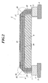
- FIG. 2 is a cross-sectional view of the optical waveguide film cable 1.
- the optical waveguide film cable 1 is constituted of a light-emitting element 3 provided on a substrate 2, a light-receiving element 5 provided on a substrate 4 and an optical guide member 6 extending in an optical guide direction (in FIG. 2 , right direction).
- the light-emitting element 3 and the optical guide member 6, and the light-receiving element 5 and the optical guide member 6 are adhered with each other by optical path members 7, 8 respectively.
- the optical path members 7, 8 have a function to adhere and fix the light-emitting element 3 and the light-receiving element 5 to the optical guide member 6 and a function as a refractive medium to stabilize transmission of light.
- the optical guide member 6 has a film-like shape and flexibility, and is constituted of a clad section 9, a core section 10 formed in the clad section 9 and protective layers 11, 12.
- a refractive index of the core section 10 is higher than a refractive index of the clad section 9 and a refractive index of air.
- the light propagated through the core section 10 is totally reflected at the interface with the clad section 9 or the air.
- a side face of the clad section 9 is covered with protective films 11, 12.
- the core section 10 includes a body portion 13 extending in an optical guide direction, and a light inlet portion 14 and a light exit portion 15 protruding from both ends of the body portion 13 in a direction substantially orthogonal to the body portion 13, and is formed in a substantial U-shape.
- the light inlet portion 14 and the light exit portion 15 are the light inlet and exit portions described in the claims.
- Mirror faces 18, 19 which are inclined planes having an inclination angle of 45° are formed on a shoulder portion 16 located at the continuous portion of a body portion 13 and a light inlet portion 14, and on a shoulder portion 17 located at the continuous portion of the body portion 13 and a light exit portion 15, respectively.
- the core section 10 is exposed outside the clad section 9 and in contact with the outside air at these mirror faces 18, 19.
- a cross-section of the core section 10 in a direction perpendicular to the direction light propagates through the core section 10 is formed in a square shape.
- the light-emitting element 3 is provided on an end of the light inlet section 14.
- the light-emitting element 3 is constituted of, for example, a surface emitting semiconductor laser (VCSEL: Vertical Cavity Surface Emitting Laser), and according to an electrical signal supplied externally, emits light in a direction perpendicular to the contact face with the optical guide member 6 (in FIG. 2 , upward).
- VCSEL Vertical Cavity Surface Emitting Laser
- the light-receiving element 5 is provided on an end of the light exit portion 15.
- the light-receiving element 5 is constituted of, for example, PD (PhotoDiode) and receives light in a direction perpendicular to the contact face with the optical guide member 6 (in FIG. 2 , downward) to convert to an electrical signal.
- PD PhotoDiode
- the light emitted from the light-emitting element 3 propagates through the light inlet portion 14 of the core section 10 and is reflected totally by the mirror face 18.
- Light subjected to optical path change by 90° on the mirror face 18 propagates through the body portion 13 of the core section 10 and is reflected totally by the mirror surface 19.
- Light subjected to optical path change by 90° on the mirror surface 19 propagates through the light exit portion 15 of the core section 10 and is received by the light-receiving element 5.
- a resin thin film in a liquid state is formed on the protective film 11 with a rotating film formation method, etc., and the film is heated to form a clad layer 9a.
- the protective film 11 is constituted of a resin film, for example, polyimide, PET, etc.
- the clad layer 9a includes polymeric resin material with optical transparency, and is constituted of, for example, epoxy resin, acrylic resin, imide resin, etc.
- the core layer 10a includes polymeric resin material with optical transparency and is constituted of, for example, epoxy resin, acrylic resin, imide resin, etc.
- a mask is applied to the core layer 10a, and as shown in FIG. 3C , a core pattern of the core section 10 is formed in a two-dimensional state with photolithography and etching processing.
- "Formed in a two-dimensional state” means to form a two-dimensional pattern with a plane parallel to an XY plane including arrows X, Y shown in FIG. 3C .
- the core section 10 is formed along a plane of the clad layer 9a. As shown in FIG.
- the core section 10 is substantially U-shaped, includes the body portion 13, the light inlet portion 14 and a light exit portion 15 and includes mirror faces 18, 19 on a shoulder portion 16 located at the continuous portion of a body portion 13 and a light inlet portion 14, and on a shoulder portion 17 located at the continuous portion of the body portion 13 and a light exit portion 15, respectively.
- a resin thin film in a liquid state is formed with a rotating film formation method, etc., and the film is heated to cover the core section 10 with a material which has a refractive index as same as the clad layer 9a to form a clad layer 9b.
- the clad layer 9b is formed with a material with a same composition as the clad layer 9a.
- a protective film 12 is formed on the clad layer 9b.
- the protective film 12 is constituted of a resin film, for example, polyimide, PET, etc.
- FIG. 4B shows a cross-section taken along A-A shown in FIG. 4A .
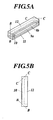
- FIG. 5A and FIG. 5B are a perspective view and a top view showing layers shown in FIG. 4A by cutting out in a rectangular shape to include core section 10.
- the mirror faces 18, 19 of the core section 10 are exposed to the outside.
- an optical guide member 6 shown in FIG. 6A and FIG. 6B is completed.
- the clad layer 9a and the clad layer 9b shown in FIG. 6A correspond to the clad section 9 shown in FIG. 1 and FIG. 2 .
- the protective layer 11, the clad layer 9a, the clad layer 9b and the protective layer 12 may be cut in a direction perpendicular to the layers with a dicer or a laser as a method of processing for exposing the mirror faces 18, 19.
- the unnecessary portions may also be dissolved by liquid phase etching or gas phase etching processing on the layers, protective layer 11, the clad layer 9a, the clad layer 9b and the protective layer 12.
- the optical waveguide film cable 1 is completed.
- the light may be directly introduced to the core section 10 from a substantially orthogonal direction to the optical guide direction, and the light may directly exit from the core section 10 in a substantially orthogonal direction to the optical guide direction. Consequently, since the light does not pass through a portion where a refractive index is different, scattering and reflecting on an interface may be avoided, and optical loss may be reduced. Also, the length of the light inlet portion 14 and the light exit portion 15 of the core section 10 may be set freely.
- the above-described embodiment is an example of the optical waveguide device of the present invention, and thus is not limited to the embodiments shown. Details of the components constituting the optical waveguide film cable 1 may be modified without leaving the scope of the invention.
- the angle of the mirror faces 18, 19 are formed at 45°, however, the angle of the mirror faces 18, 19 are not limited to this angle, and the angle may be adjusted to an angle so that the light loss becomes a minimum according to a characteristic of the light-emitting element 3 or the light-receiving element 5.
- the substantially U-shaped core section 10 is formed in a two-dimensional shape, however, the shape is not limited to a U-shape, and a V-shaped, M-shaped, N-shaped, etc. two-dimensional pattern may be formed.
- the method of forming the core pattern is not limited to photolithography and etching processing, and direct lithography may also be used.
- the light-emitting element 3 and the light-receiving element 5 are respectively provided on different substrates 2, 4, however, the light-emitting element 3 and the light-receiving element 5 may be provided on the same substrate.
- optical waveguide device and the method for fabricating the optical waveguide device of the present invention may be applied to the field of optical communication.
Landscapes
- Physics & Mathematics (AREA)
- General Physics & Mathematics (AREA)
- Optics & Photonics (AREA)
- Engineering & Computer Science (AREA)
- Microelectronics & Electronic Packaging (AREA)
- Optical Integrated Circuits (AREA)
- Optical Couplings Of Light Guides (AREA)
Abstract
An optical waveguide device in which optical loss is reduced. An optical waveguide film cable (1) is constituted of a light-emitting element (3), a light-receiving element (5), and an optical guide member (6). The optical guide member (6) has a film-like shape and a substantially U-shaped core section (10) is formed in a clad section (9). Mirror faces (18, 19) having an inclination angle of 45° are formed on a shoulder portion (16) located at the continuous portion of a body portion (13) and a light inlet portion (14), and on a shoulder portion (17) located at the continuous portion of the body portion (13) and a light exit portion (15). Light emitted from the light-emitting element (3) propagates through the light inlet portion (14) of the core section (10) and is reflected totally by the mirror surface (18). Light subjected to optical path change by 90° on the mirror surface (18) propagates through the body portion (13) of the core section (10) and is reflected totally by the mirror surface (19). Light subjected to optical path change by 90° on the mirror surface (19) propagates through the exit portion (15) of the core section (10) and is received by the light-receiving element (5).
Description
- The present invention relates to an optical waveguide device and a method for fabricating an optical waveguide device.
- Recently, as a component for optical communication, an optical waveguide device which uses polymer resin material is used. In order to change a direction of optical wiring in an optical waveguide, a technique where an end of the optical waveguide forms an inclination surface by 45° and the inclination surface bends an optical path in a right angle is developed (for example, Patent Document 1).
-
Fig. 7 shows a cross-sectional view of anoptical waveguide device 31. As shown inFig. 7 , theoptical waveguide device 31 is constituted of a light-emittingelement 33 provided on asubstrate 32, a light-receivingelement 35 provided on asubstrate 34, and anoptical guide member 36 for guiding the light. The light-emittingelement 33 and anoptical guide member 36, and the light-receivingelement 35 and theoptical guide member 36 are adhered to each other withoptical path members - The
optical guide member 36 includes, from the bottom, aprotective layer 39, aclad section 40, and aprotective layer 41, and acore section 42 with a higher refractive index than theclad section 40 is formed in theclad section 40. Mirror faces 43, 44 having an inclination angle of 45° are formed on both ends of theoptical guide member 36. The mirror faces 43, 44 are formed by cutting using an angled blade having an inclination angle on its blade edge. As shown inFIG. 7 , light emitted from the light-emittingelement 33 is reflected totally by themirror face 43 and progresses through thecore section 42. Then, the light is reflected totally by themirror face 44 and is received by the light-receivingelement 35. - Other than the total reflection mirror method shown in
FIG. 7 , a mirror block method for changing an optical path as shown inFIG. 8 is used. InFIG. 8 , the same reference numerals are applied to the same components as inFIG. 7 , and description of the structure is omitted. As shown inFig. 8 , the light which propagated through thecore section 42 is reflected by themirror face 45 and the light is received by the light-receivingelement 35. In the mirror block method, it is preferable to coat the surface of themirror face 45 with metal in order to increase reflection efficiency.
Patent Document 1: Japanese Patent Application Laid-Open Publication No.2001-166167 - However, in
Fig. 7 , in order for the light emitted from the light-emittingelement 33 to reach thecore section 42, the light needs to pass through theoptical path member 37, theprotective layer 39, and theclad section 40, causing light loss through optical diffusion and interface reflection. Similarly, light loss occurred when the light reached the light-receivingelement 35 from thecore section 42. In order to prevent light loss, highly accurate adjustment of the position in the height direction was necessary. - Since the mirror faces 43, 44 totally reflect the light with a refractive index difference between the
core section 42 and air, as shown inFIG. 9 , there was a problem of when theoptical path member 37 adheres to themirror face 43, the light leaks. Also, the mirror faces 43, 44 are formed by cutting using an angled blade, in which rotary instability easily occurs due to blade thickness, and it was necessary to carefully control the accuracy of the angle. - The present invention has been made in consideration of the above problems of the techniques, and it is an object to reduce light loss in an optical waveguide device.
- In order to achieve the above object, according to a first aspect of the present invention, there is provided an optical waveguide device, comprising:
- an optical guide member extending in an optical guide direction with a core section in a clad section, wherein
- the core section is formed in a substantial U-shape of a two-dimensional shape including;
- a body portion; and
- light inlet and exit portions which protrude from both ends of the body portion in a direction substantially orthogonal to the body portion;
- inclined planes are formed on shoulder portions located at continuous portions of the body portion and the light inlet and exit portions; and
- the inclined planes of the core section are exposed outside.
- Preferably, the optical guide member is formed in a film-like shape.
- Preferably, ends of the light inlet and exit portions of the core section are provided with photoelectric conversion elements to perform a conversion between light and electricity.
- Preferably, one of the photoelectric conversion elements provided on one end of the light inlet and exit portions is a light-emitting element, and the other of the photoelectric conversion elements provided on the other end of the light inlet and exit portions is a light-receiving element.
- According to a second aspect of the present invention, there is provided a method for fabricating an optical waveguide device, comprising the steps of:
- forming a first clad layer;
- forming a core section formed in a substantial U-shape of a two-dimensional shape on the first clad layer, including a body portion and light inlet and exit portions which protrude from both ends of the body portion in a direction substantially orthogonal to the body portion, in which inclined planes are formed on shoulder portions located at continuous portions of the body portion and the light inlet and exit portions;
- forming a second clad layer which covers the core section and has a refractive index as same as the first clad layer; and
- exposing the inclined planes of the core section outside.
- Preferably, the inclined planes of the core section are exposed by cutting the first clad layer and the second clad layer in a direction orthogonal to the layers.
- Preferably, the inclined planes of the core section are exposed by etching processing performed on the first clad layer and the second clad layer.
- According to the present invention, by totally reflecting light on an inclined plane and propagating the light along the substantially U-shaped core section, the light may be directly introduced to the core section from a substantially orthogonal direction to the optical guide direction, and the light directly exits from the core section in a direction substantially orthogonal to the optical guide direction. Consequently, since the light does not pass through a portion where a refractive index is different, scattering and reflecting on an interface can be avoided, and optical loss can be reduced.
-
-
FIG. 1 is a perspective view showing an optical waveguide film cable 1 of the embodiment of the present invention; -
FIG. 2 is a cross-sectional view showing the optical waveguide film cable 1; -
FIG. 3A is a diagram for describing a forming of aclad layer 9a; -
FIG. 3B is a diagram for describing a forming of acore layer 10a; -
FIG. 3C is a diagram for describing a forming of acore section 10; -
FIG. 3D is a diagram showing a shape of thecore section 10; -
FIG. 4A is a diagram for describing a method of forming theclad layer 9b and aprotective layer 12; -
FIG. 4B is a diagram showing a cross-section taken along A-A shown inFIG. 4A ; -
FIG. 5A is a perspective view showing layers by cutting out in a rectangular shape to include thecore section 10; -
FIG. 5B is a top view showing layers by cutting out in a rectangular shape to include thecore section 10; -
FIG. 6A is a perspective view showing mirror faces 18, 19 in an exposed state; -
FIG. 6B is a top view showing the mirror faces 18, 19 in an exposed state; -
FIG. 7 is a cross-sectional view showing anoptical waveguide device 31; -
FIG. 8 is a diagram for describing a mirror block method to change an optical path; and -
FIG. 9 is a diagram for describing a problem in theoptical waveguide device 31. - An embodiment of the present invention will be specifically described with reference to the drawings.
-
FIG. 1 is a perspective view showing an optical waveguide film cable 1 of the embodiment of the present invention andFIG. 2 is a cross-sectional view of the optical waveguide film cable 1. As shown inFIG. 1 andFIG. 2 , the optical waveguide film cable 1 is constituted of a light-emittingelement 3 provided on asubstrate 2, a light-receivingelement 5 provided on a substrate 4 and anoptical guide member 6 extending in an optical guide direction (inFIG. 2 , right direction). The light-emittingelement 3 and theoptical guide member 6, and the light-receivingelement 5 and theoptical guide member 6 are adhered with each other byoptical path members optical path members element 3 and the light-receivingelement 5 to theoptical guide member 6 and a function as a refractive medium to stabilize transmission of light. - The
optical guide member 6 has a film-like shape and flexibility, and is constituted of aclad section 9, acore section 10 formed in theclad section 9 andprotective layers core section 10 is higher than a refractive index of theclad section 9 and a refractive index of air. Thus, the light propagated through thecore section 10 is totally reflected at the interface with theclad section 9 or the air. A side face of theclad section 9 is covered withprotective films - As shown in
FIG. 2 , thecore section 10 includes abody portion 13 extending in an optical guide direction, and alight inlet portion 14 and alight exit portion 15 protruding from both ends of thebody portion 13 in a direction substantially orthogonal to thebody portion 13, and is formed in a substantial U-shape. Thelight inlet portion 14 and thelight exit portion 15 are the light inlet and exit portions described in the claims. Mirror faces 18, 19 which are inclined planes having an inclination angle of 45° are formed on ashoulder portion 16 located at the continuous portion of abody portion 13 and alight inlet portion 14, and on ashoulder portion 17 located at the continuous portion of thebody portion 13 and alight exit portion 15, respectively. Thecore section 10 is exposed outside theclad section 9 and in contact with the outside air at these mirror faces 18, 19. A cross-section of thecore section 10 in a direction perpendicular to the direction light propagates through thecore section 10 is formed in a square shape. - The light-emitting
element 3 is provided on an end of thelight inlet section 14. The light-emittingelement 3 is constituted of, for example, a surface emitting semiconductor laser (VCSEL: Vertical Cavity Surface Emitting Laser), and according to an electrical signal supplied externally, emits light in a direction perpendicular to the contact face with the optical guide member 6 (inFIG. 2 , upward). - The light-receiving
element 5 is provided on an end of thelight exit portion 15. The light-receivingelement 5 is constituted of, for example, PD (PhotoDiode) and receives light in a direction perpendicular to the contact face with the optical guide member 6 (inFIG. 2 , downward) to convert to an electrical signal. - As shown in
FIG. 2 , the light emitted from the light-emittingelement 3 propagates through thelight inlet portion 14 of thecore section 10 and is reflected totally by themirror face 18. Light subjected to optical path change by 90° on themirror face 18 propagates through thebody portion 13 of thecore section 10 and is reflected totally by themirror surface 19. Light subjected to optical path change by 90° on themirror surface 19 propagates through thelight exit portion 15 of thecore section 10 and is received by the light-receivingelement 5. - Next, a method for fabricating an optical waveguide film cable 1 will be described with reference to
FIG. 3A, FIG. 3B ,FIG. 3C, FIG. 3D ,FIG. 4A, FIG. 4B ,FIG. 5A, FIG. 5B ,FIG. 6A and FIG. 6B . - First, as shown in
FIG. 3A , a resin thin film in a liquid state is formed on theprotective film 11 with a rotating film formation method, etc., and the film is heated to form aclad layer 9a. Theprotective film 11 is constituted of a resin film, for example, polyimide, PET, etc. Theclad layer 9a includes polymeric resin material with optical transparency, and is constituted of, for example, epoxy resin, acrylic resin, imide resin, etc. - Then, as shown in
FIG. 3B , a resin thin film in a liquid state is formed on theclad layer 9a with a rotating film formation method, etc., and the film is heated to form acore layer 10a with a higher refractive index than theclad layer 9a. Thecore layer 10a includes polymeric resin material with optical transparency and is constituted of, for example, epoxy resin, acrylic resin, imide resin, etc. - Next, a mask is applied to the
core layer 10a, and as shown inFIG. 3C , a core pattern of thecore section 10 is formed in a two-dimensional state with photolithography and etching processing. "Formed in a two-dimensional state" means to form a two-dimensional pattern with a plane parallel to an XY plane including arrows X, Y shown inFIG. 3C . In short, thecore section 10 is formed along a plane of theclad layer 9a. As shown inFIG. 3D , thecore section 10 is substantially U-shaped, includes thebody portion 13, thelight inlet portion 14 and alight exit portion 15 and includes mirror faces 18, 19 on ashoulder portion 16 located at the continuous portion of abody portion 13 and alight inlet portion 14, and on ashoulder portion 17 located at the continuous portion of thebody portion 13 and alight exit portion 15, respectively. - Next, as shown in
FIG. 4A , a resin thin film in a liquid state is formed with a rotating film formation method, etc., and the film is heated to cover thecore section 10 with a material which has a refractive index as same as theclad layer 9a to form aclad layer 9b. It is preferable that theclad layer 9b is formed with a material with a same composition as theclad layer 9a. As shown inFIG. 4a , aprotective film 12 is formed on theclad layer 9b. Theprotective film 12 is constituted of a resin film, for example, polyimide, PET, etc.FIG. 4B shows a cross-section taken along A-A shown inFIG. 4A . -
FIG. 5A and FIG. 5B are a perspective view and a top view showing layers shown inFIG. 4A by cutting out in a rectangular shape to includecore section 10. By processing the layers perpendicular to the layers at the position of B-B, C-C shown inFIG. 5A and FIG. 5B , the mirror faces 18, 19 of thecore section 10 are exposed to the outside. In this way, anoptical guide member 6 shown inFIG. 6A and FIG. 6B is completed. Theclad layer 9a and theclad layer 9b shown inFIG. 6A correspond to theclad section 9 shown inFIG. 1 andFIG. 2 . - The
protective layer 11, theclad layer 9a, theclad layer 9b and theprotective layer 12 may be cut in a direction perpendicular to the layers with a dicer or a laser as a method of processing for exposing the mirror faces 18, 19. The unnecessary portions may also be dissolved by liquid phase etching or gas phase etching processing on the layers,protective layer 11, theclad layer 9a, theclad layer 9b and theprotective layer 12. - As shown in
FIG. 1 andFIG. 2 , by adhering the light-emittingelement 3 and the light-receivingelement 5 to theoptical guide member 6 with optical path members, 7, 8, the optical waveguide film cable 1 is completed. - As described above, according to the present embodiment, by totally reflecting light by mirror faces 18, 19 and propagating the light along a
core section 10 substantially U-shaped, the light may be directly introduced to thecore section 10 from a substantially orthogonal direction to the optical guide direction, and the light may directly exit from thecore section 10 in a substantially orthogonal direction to the optical guide direction. Consequently, since the light does not pass through a portion where a refractive index is different, scattering and reflecting on an interface may be avoided, and optical loss may be reduced. Also, the length of thelight inlet portion 14 and thelight exit portion 15 of thecore section 10 may be set freely. - When the mirror faces 18, 19 are exposed by cutting with a dicer, since the processing may be performed with the same thin blade as used in cutting the external form of the
optical guide member 6, processing with high accuracy may be easily performed, and a number of steps such as changing blades, etc. may be reduced compared to the method of processing using an angled blade. - The above-described embodiment is an example of the optical waveguide device of the present invention, and thus is not limited to the embodiments shown. Details of the components constituting the optical waveguide film cable 1 may be modified without leaving the scope of the invention.
- For example, in the above-described embodiment, the angle of the mirror faces 18, 19 are formed at 45°, however, the angle of the mirror faces 18, 19 are not limited to this angle, and the angle may be adjusted to an angle so that the light loss becomes a minimum according to a characteristic of the light-emitting
element 3 or the light-receivingelement 5. In the above-described embodiment, the substantiallyU-shaped core section 10 is formed in a two-dimensional shape, however, the shape is not limited to a U-shape, and a V-shaped, M-shaped, N-shaped, etc. two-dimensional pattern may be formed. - The method of forming the core pattern is not limited to photolithography and etching processing, and direct lithography may also be used.
- In the above-described embodiment, the light-emitting
element 3 and the light-receivingelement 5 are respectively provided ondifferent substrates 2, 4, however, the light-emittingelement 3 and the light-receivingelement 5 may be provided on the same substrate. - The optical waveguide device and the method for fabricating the optical waveguide device of the present invention may be applied to the field of optical communication.
-
- 1
- optical waveguide film cable (optical waveguide device)
- 3
- light-emitting element
- 5
- light-receiving element
- 6
- optical guide member
- 7, 8
- optical path members
- 9
- clad section
- 9a
- clad layer (first clad layer)
- 9b
- clad layer (second clad layer)
- 10
- core section
- 10a
- core layer
- 11, 12
- protective layers
- 13
- body portion
- 14
- light inlet portion (light inlet and exit portion)
- 15
- light exit portion (light inlet and exit portion)
- 16, 17
- shoulder portions
- 18, 19
- mirror faces (inclined planes)
- 31
- optical waveguide device
- 33
- light-emitting element
- 35
- light-receiving element
- 36
- optical guide member
- 37, 38
- optical path member
- 39
- protective layer
- 40
- clad section
- 41
- protective layer
- 42
- core section
- 43, 44
- mirror faces
- 45
- mirror face
Claims (7)
- An optical waveguide device comprising:an optical guide member extending in an optical guide direction with a core section in a clad section, whereinthe core section is formed in a substantial U-shape of a two-dimensional shape including;a body portion; andlight inlet and exit portions which protrude from both ends of the body portion in a direction substantially orthogonal to the body portion;inclined planes are formed on shoulder portions located at continuous portions of the body portion and the light inlet and exit portions; andthe inclined planes of the core section are exposed outside.
- The optical waveguide device according to claim 1, wherein the optical guide member is formed in a film-like shape.
- The optical waveguide device according to either claim 1 or 2, wherein ends of the light inlet and exit portions of the core section are provided with photoelectric conversion elements to perform a conversion between light and electricity.
- The optical waveguide device according to claim 3, wherein, one of the photoelectric conversion elements provided on one end of the light inlet and exit portions is a light-emitting element, and the other of the photoelectric conversion elements provided on the other end of the light inlet and exit portions is a light-receiving element.
- A method for fabricating an optical waveguide device, comprising the steps of:forming a first clad layer;forming a core section formed in a substantial U-shape of a two-dimensional shape on the first clad layer, including a body portion and light inlet and exit portions which protrude from both ends of the body portion in a direction substantially orthogonal to the body portion, in which inclined planes are formed on shoulder portions located at continuous portions of the body portion and the light inlet and exit portions;forming a second clad layer which covers the core section and has a refractive index as same as the first clad layer; andexposing the inclined planes of the core section outside.
- A method for fabricating an optical waveguide device according to claim 5, wherein the inclined planes of the core section are exposed by cutting the first clad layer and the second clad layer in a direction orthogonal to the layers.
- A method for fabricating an optical waveguide device according to claim 5, wherein the inclined planes of the core section are exposed by etching processing performed on the first clad layer and the second clad layer.
Applications Claiming Priority (2)
| Application Number | Priority Date | Filing Date | Title |
|---|---|---|---|
| JP2005286723A JP4277840B2 (en) | 2005-09-30 | 2005-09-30 | Manufacturing method of optical waveguide device |
| PCT/JP2006/312383 WO2007039964A1 (en) | 2005-09-30 | 2006-06-21 | Optical waveguide device and method for fabricating optical waveguide device |
Publications (2)
| Publication Number | Publication Date |
|---|---|
| EP1930755A1 true EP1930755A1 (en) | 2008-06-11 |
| EP1930755A4 EP1930755A4 (en) | 2009-10-28 |
Family
ID=37906010
Family Applications (1)
| Application Number | Title | Priority Date | Filing Date |
|---|---|---|---|
| EP06767042A Withdrawn EP1930755A4 (en) | 2005-09-30 | 2006-06-21 | Optical waveguide device and method for fabricating optical waveguide device |
Country Status (6)
| Country | Link |
|---|---|
| US (1) | US20090232465A1 (en) |
| EP (1) | EP1930755A4 (en) |
| JP (1) | JP4277840B2 (en) |
| KR (1) | KR100970395B1 (en) |
| CN (1) | CN101243341A (en) |
| WO (1) | WO2007039964A1 (en) |
Cited By (1)
| Publication number | Priority date | Publication date | Assignee | Title |
|---|---|---|---|---|
| US7974508B2 (en) | 2009-02-03 | 2011-07-05 | Nitto Denko Corporation | Multi-layer structure and method for manufacturing the same |
Families Citing this family (2)
| Publication number | Priority date | Publication date | Assignee | Title |
|---|---|---|---|---|
| EP1909123A4 (en) * | 2005-07-27 | 2009-07-08 | Mitsumi Electric Co Ltd | FLAT GUIDE FLAT CABLE |
| CN108227067B (en) | 2017-11-13 | 2021-02-02 | 南京矽力微电子技术有限公司 | Optical structure and electronic equipment with same |
Family Cites Families (14)
| Publication number | Priority date | Publication date | Assignee | Title |
|---|---|---|---|---|
| JPS59168414A (en) * | 1983-03-16 | 1984-09-22 | Nec Corp | Reflection type multichannel optical switch |
| CA1211550A (en) * | 1984-03-22 | 1986-09-16 | Northern Telecom Limited | Electronic apparatus with circuit cards and signals optically coupled therebetween |
| US4733093A (en) * | 1984-03-26 | 1988-03-22 | Northern Telecom Limited | Electronic apparatus with circuit cards and signals optically coupled therebetween |
| US6324313B1 (en) * | 1998-12-21 | 2001-11-27 | Lsi Logic Corporation | On-chip multiple layer vertically transitioning optical waveguide and damascene method of fabricating the same |
| TW451084B (en) * | 1999-06-25 | 2001-08-21 | Toppan Printing Co Ltd | Optical-electro wiring board, mounted board, and manufacturing method of optical-electro wiring board |
| US6713866B2 (en) * | 2002-04-22 | 2004-03-30 | Agilent Technologies, Inc. | Cooling of optoelectronic elements |
| JP3883901B2 (en) * | 2002-04-23 | 2007-02-21 | 三菱電機株式会社 | Optical path conversion device and manufacturing method thereof |
| EP1372005A3 (en) * | 2002-06-07 | 2004-11-17 | Fuji Photo Film Co., Ltd. | Optical integrated circuit and method of fabrication |
| JP2004133300A (en) * | 2002-10-11 | 2004-04-30 | Sony Corp | Waveguide mold and method of manufacturing waveguide |
| JP2004191564A (en) * | 2002-12-10 | 2004-07-08 | Mitsubishi Electric Corp | Optical path conversion connector |
| US7263248B2 (en) * | 2003-02-11 | 2007-08-28 | Avago Technologies Fiber Ip (Singapore) Pte. Ltd. | Optical via to pass signals through a printed circuit board |
| US7324723B2 (en) * | 2003-10-06 | 2008-01-29 | Mitsui Chemicals, Inc. | Optical waveguide having specular surface formed by laser beam machining |
| US7224857B2 (en) * | 2004-12-20 | 2007-05-29 | Fujitsu Limited | Optical-routing boards for opto-electrical systems and methods and apparatuses for manufacturing the same |
| US20070258675A1 (en) * | 2006-05-05 | 2007-11-08 | Virgin Islands Microsystems, Inc. | Multiplexed optical communication between chips on a multi-chip module |
-
2005
- 2005-09-30 JP JP2005286723A patent/JP4277840B2/en not_active Expired - Fee Related
-
2006
- 2006-06-21 KR KR1020087003381A patent/KR100970395B1/en not_active Expired - Fee Related
- 2006-06-21 WO PCT/JP2006/312383 patent/WO2007039964A1/en not_active Ceased
- 2006-06-21 US US11/992,722 patent/US20090232465A1/en not_active Abandoned
- 2006-06-21 CN CNA2006800297365A patent/CN101243341A/en active Pending
- 2006-06-21 EP EP06767042A patent/EP1930755A4/en not_active Withdrawn
Cited By (1)
| Publication number | Priority date | Publication date | Assignee | Title |
|---|---|---|---|---|
| US7974508B2 (en) | 2009-02-03 | 2011-07-05 | Nitto Denko Corporation | Multi-layer structure and method for manufacturing the same |
Also Published As
| Publication number | Publication date |
|---|---|
| JP4277840B2 (en) | 2009-06-10 |
| KR20080026213A (en) | 2008-03-24 |
| WO2007039964A1 (en) | 2007-04-12 |
| US20090232465A1 (en) | 2009-09-17 |
| KR100970395B1 (en) | 2010-07-15 |
| CN101243341A (en) | 2008-08-13 |
| JP2007094303A (en) | 2007-04-12 |
| EP1930755A4 (en) | 2009-10-28 |
Similar Documents
| Publication | Publication Date | Title |
|---|---|---|
| EP1522882B1 (en) | Optical waveguide having mirror surface formed by laser beam machining | |
| US7590315B2 (en) | Optical waveguide and optical module using the same | |
| KR101588348B1 (en) | Photonic guiding device | |
| EP2803123B1 (en) | Integrated sub-wavelength grating system | |
| JP5208351B2 (en) | Optical device | |
| JP5089643B2 (en) | Optical connection element manufacturing method, optical transmission board, optical connection component, connection method, and optical transmission system | |
| JP5309212B2 (en) | Optical splitter device | |
| US7796851B2 (en) | Manufacturing method of optical waveguide, optical waveguide and optical reception/transmission apparatus | |
| US20010053260A1 (en) | Optical module and method for producing the same, and optical circuit device | |
| EP2012154A1 (en) | Optical device and optical device manufacturing method | |
| US7460747B2 (en) | Waveguide and optical cable module | |
| US10302871B2 (en) | Microfabricated fiber optic platform | |
| US7747115B2 (en) | Optical waveguide device and light outputting module | |
| US8358892B2 (en) | Connection structure of two-dimensional array optical element and optical circuit | |
| US20170371100A1 (en) | Optical waveguide and manufacturing method thereof, optical device using the optical waveguide | |
| SE525405C2 (en) | Mirrors for polymeric guides, process for their preparation, and optical waveguide device | |
| US20090232465A1 (en) | Optical Waveguide Device and Method for Fabricating Optical Waveguide Device | |
| JP2007072007A (en) | Optical waveguide module | |
| EP1930756A1 (en) | Optical waveguide device and method for fabricating optical waveguide device | |
| JP4609311B2 (en) | Optical transceiver | |
| JP7750288B2 (en) | Optical connection structure and manufacturing method thereof | |
| Hwang et al. | Bendable and splitter-integrated optical subassembly based on a flexible optical board | |
| JP2006349861A (en) | Optical waveguide, optical module, and optical waveguide manufacturing method | |
| JP2009025552A (en) | Optical waveguide and method for manufacturing the same | |
| JP2013127641A (en) | Optical splitter device |
Legal Events
| Date | Code | Title | Description |
|---|---|---|---|
| PUAI | Public reference made under article 153(3) epc to a published international application that has entered the european phase |
Free format text: ORIGINAL CODE: 0009012 |
|
| 17P | Request for examination filed |
Effective date: 20080326 |
|
| AK | Designated contracting states |
Kind code of ref document: A1 Designated state(s): DE FR GB |
|
| RBV | Designated contracting states (corrected) |
Designated state(s): DE FR GB |
|
| A4 | Supplementary search report drawn up and despatched |
Effective date: 20090925 |
|
| STAA | Information on the status of an ep patent application or granted ep patent |
Free format text: STATUS: THE APPLICATION HAS BEEN WITHDRAWN |
|
| 18W | Application withdrawn |
Effective date: 20110111 |