EP1928219A2 - Imaging apparatus for fully automatic screen printer - Google Patents
Imaging apparatus for fully automatic screen printer Download PDFInfo
- Publication number
- EP1928219A2 EP1928219A2 EP07253746A EP07253746A EP1928219A2 EP 1928219 A2 EP1928219 A2 EP 1928219A2 EP 07253746 A EP07253746 A EP 07253746A EP 07253746 A EP07253746 A EP 07253746A EP 1928219 A2 EP1928219 A2 EP 1928219A2
- Authority
- EP
- European Patent Office
- Prior art keywords
- stacked
- imaging apparatus
- fully automatic
- beamsplitters
- light source
- Prior art date
- Legal status (The legal status is an assumption and is not a legal conclusion. Google has not performed a legal analysis and makes no representation as to the accuracy of the status listed.)
- Granted
Links
Images


Classifications
-
- H—ELECTRICITY
- H05—ELECTRIC TECHNIQUES NOT OTHERWISE PROVIDED FOR
- H05K—PRINTED CIRCUITS; CASINGS OR CONSTRUCTIONAL DETAILS OF ELECTRIC APPARATUS; MANUFACTURE OF ASSEMBLAGES OF ELECTRICAL COMPONENTS
- H05K3/00—Apparatus or processes for manufacturing printed circuits
- H05K3/0008—Apparatus or processes for manufacturing printed circuits for aligning or positioning of tools relative to the circuit board
-
- G—PHYSICS
- G01—MEASURING; TESTING
- G01N—INVESTIGATING OR ANALYSING MATERIALS BY DETERMINING THEIR CHEMICAL OR PHYSICAL PROPERTIES
- G01N21/00—Investigating or analysing materials by the use of optical means, i.e. using sub-millimetre waves, infrared, visible or ultraviolet light
- G01N21/84—Systems specially adapted for particular applications
- G01N21/88—Investigating the presence of flaws or contamination
- G01N21/8806—Specially adapted optical and illumination features
-
- G—PHYSICS
- G01—MEASURING; TESTING
- G01N—INVESTIGATING OR ANALYSING MATERIALS BY DETERMINING THEIR CHEMICAL OR PHYSICAL PROPERTIES
- G01N21/00—Investigating or analysing materials by the use of optical means, i.e. using sub-millimetre waves, infrared, visible or ultraviolet light
- G01N21/84—Systems specially adapted for particular applications
- G01N21/88—Investigating the presence of flaws or contamination
- G01N21/95—Investigating the presence of flaws or contamination characterised by the material or shape of the object to be examined
- G01N21/956—Inspecting patterns on the surface of objects
-
- H—ELECTRICITY
- H05—ELECTRIC TECHNIQUES NOT OTHERWISE PROVIDED FOR
- H05K—PRINTED CIRCUITS; CASINGS OR CONSTRUCTIONAL DETAILS OF ELECTRIC APPARATUS; MANUFACTURE OF ASSEMBLAGES OF ELECTRICAL COMPONENTS
- H05K1/00—Printed circuits
- H05K1/02—Details
- H05K1/0266—Marks, test patterns or identification means
- H05K1/0269—Marks, test patterns or identification means for visual or optical inspection
-
- H—ELECTRICITY
- H05—ELECTRIC TECHNIQUES NOT OTHERWISE PROVIDED FOR
- H05K—PRINTED CIRCUITS; CASINGS OR CONSTRUCTIONAL DETAILS OF ELECTRIC APPARATUS; MANUFACTURE OF ASSEMBLAGES OF ELECTRICAL COMPONENTS
- H05K2201/00—Indexing scheme relating to printed circuits covered by H05K1/00
- H05K2201/09—Shape and layout
- H05K2201/09818—Shape or layout details not covered by a single group of H05K2201/09009 - H05K2201/09809
- H05K2201/09918—Optically detected marks used for aligning tool relative to the PCB, e.g. for mounting of components
-
- H—ELECTRICITY
- H05—ELECTRIC TECHNIQUES NOT OTHERWISE PROVIDED FOR
- H05K—PRINTED CIRCUITS; CASINGS OR CONSTRUCTIONAL DETAILS OF ELECTRIC APPARATUS; MANUFACTURE OF ASSEMBLAGES OF ELECTRICAL COMPONENTS
- H05K3/00—Apparatus or processes for manufacturing printed circuits
- H05K3/10—Apparatus or processes for manufacturing printed circuits in which conductive material is applied to the insulating support in such a manner as to form the desired conductive pattern
- H05K3/12—Apparatus or processes for manufacturing printed circuits in which conductive material is applied to the insulating support in such a manner as to form the desired conductive pattern using thick film techniques, e.g. printing techniques to apply the conductive material or similar techniques for applying conductive paste or ink patterns
- H05K3/1216—Apparatus or processes for manufacturing printed circuits in which conductive material is applied to the insulating support in such a manner as to form the desired conductive pattern using thick film techniques, e.g. printing techniques to apply the conductive material or similar techniques for applying conductive paste or ink patterns by screen printing or stencil printing
Definitions
- the present invention relates to an imaging apparatus, specially relates to an imaging apparatus for the reference mark measurement and inspecting the paste solder printing; more specially relates to an imaging apparatus for the reference mark measurement of the screen and the printed circuit board during the paste solder printing of the printed circuit board of the screen printing process, and for the inspection of the screen and the printed circuit board during the paste solder printing.
- the portions of the printed circuit board desired to be printed are required to be corresponding to the holes of the screen.
- Reference mark measurement is usually used for the alignment of the screen and the printed circuit board, that is to say, signs are marked on both the screen and the printed circuit board so as to ensure that the portions of the printed circuit board desired to be printed are corresponding to the holes of the screen when the relevant signs of the screen are calibrated with respect to that of the printed circuit board.
- the simplest method of the alignment is mechanical positioning, in which the reference marks are the holes formed on the printed circuit board, and the sinker bars of the pistons of one or more cylinder-piston means are inserted into the positioning holes of the printed circuit board when positioning.
- this method is of the defects including low precision, low speed and even that there is no positioning hole due to the different positioning aperture of different printed circuit board. Therefore, this method is difficult to adapt to the development of the SMT production with high density, large output and high precision, and will fall into disuse gradually.
- the screen printer is required to be of higher precision, speed and reliability.
- the quality inspection of the solder-paste printing is mainly carried out by manual inspection.
- the manual inspection may have the problems including strong subjectivity, poor reproducibility, misjudgment and overlook due to vision fatigue, etc.
- the manual inspection is hardly qualified for the inspection requirement of SMT product line.
- the imaging apparatus of the screen printer of this type normally includes a low-angle ring light source, two light sources, a beamsplitter, an optical reflector, an imaging lens and an image sensor.
- the two light sources on different horizontal planes illuminate at different time, the light sources irradiate on the screen or the printed circuit board through the beamsplitter, and then the beams of light are reflected back to the beamsplitter and refracted to the imaging lens by the beamsplitter, and finally imaging on the image sensor is obtained.
- This method is of the advantages including simple light path and low cost.
- acquiring the images at different time may result in that the image acquiring positions of the lower image and the upper image are inconsistent; and the dimension of the apparatus in the direction of the upward and downward light path is too large, so that the distance between the printed circuit board and the screen is accordingly large when acquiring the image.
- An object of the present invention is to provide an imaging apparatus with compact structure, in which the light path is easy to adjust and the images can be acquired from the same position in upward and downward directions.
- the apparatus is used for image acquiring during the reference mark measurement of the screen and the printed circuit board, and during the inspection in the solder-paste printing process.
- An imaging apparatus for fully automatic screen printer including two stacked light sources, two stacked beamsplitters, two stacked optical reflectors, two stacked imaging lens and two stacked image sensors, wherein the two stacked optical reflectors and the two stacked light sources are correspondingly disposed on two different sides of the two beamsplitters, the two stacked imaging lens are disposed on another side of the beamsplitters different from that of the optical reflectors and the light sources, the two stacked image sensors are disposed behind the imaging lens; the optical reflectors are provided with an upward reflection plane and a downward reflection plane, the optical axes of the imaging lenses are orthogonal to that of the light sources.
- the two stacked optical reflectors and the two stacked light sources are disposed on two opposite sides of the two beamsplitters, the imaging apparatus forms a T-shaped structure.
- the two stacked optical reflectors and the stacked imaging lens are correspondingly disposed on two opposite sides of the two stacked beamsplitters, the two stacked light sources are disposed on another side of the two stacked beamsplitters different from that of the optical reflectors and the imaging lens, the imaging apparatus forms a L-shaped structure.
- angles of the light-splitting planes of the beamsplitters with respect to the axes of the imaging lenses and the axes of the light source are both 45°.
- the beamsplitter may be formed of two right angular prisms; or the beamsplitter may be formed of one or two light-splitting plates.
- the optical reflector may be formed of an isosceles right angle prism or two reflection lens or a right angle prism with two reflection planes.
- the image sensor may be formed of an analog or digital CCD camera or CMOS camera.
- the imaging apparatus further includes a ring light source
- the ring light source is formed of a LED ring light source between a printed circuit board and the optical reflector in order to provide lateral illumination for the printed circuit board, the beam of light reflected downwards by the optical reflector travels through the central hole of the ring light source and then irradiates on the printed circuit board.
- the light source and the image sensor are connected to the camera controller of the image acquiring control and processing device so as to control the switching of the light source and accordingly control the image acquiring of the screen and the printed circuit board;
- the video signal output end of the image sensor is connected to the image acquiring card of the image acquiring control and processing device, so as to convert the acquired image video signals into digital signals.
- the imaging apparatus can simultaneously capture the images in downward direction (i.e. the screen) and upward direction (i.e. the printed circuit board), so that the relative movement of the printed circuit board and the screen is minimized.
- the combination of the coaxial illumination and the side illumination can improve the quality of the reference mark image of the printed circuit board and the inspection image of the solder paste, which adapts to the image acquiring during the reference mark measurement of the screen and the printed circuit board, and during the inspection in the solder-paste printing process.
- EMBODIMENT 1 A T-type Imaging apparatus with Two Lenses for Fully Automatic Screen Printer
- the imaging apparatus for reference mark measurement and inspection of the solder-paste printing includes a first reflector 1, a second reflector 2, a low-angle ring light source 3, a first beamsplitter 4, a second beamsplitter 5, a firstLED light source 6, a second LED light source 7, a first imaging lens 8, a second imaging lens 10, a image sensor 9 and a second image sensor 10.
- the two stacked optical reflectors 1, 2 and the two stacked LED light sources 6, 7 are correspondingly disposed on two opposite sides of the two stacked beamsplitters 4, 5.
- the two stacked imaging lens 8, 10 are disposed on another side of the beamsplitters 4, 5 different from that of the optical reflectors and the light sources.
- the optical axes of the two stacked image sensors 8, 10 are orthogonal to that of the LED light sources 6, 7.
- the angles of the light-splitting planes of the two beamsplitters with respect to the axes of the two imaging lenses and the axes of the two light sources are both 45°.
- the beams of light from the first LED light source 6 and the second LED light source 7 are refracted to the first reflector 1 and the second reflector 2 by the first beamsplitter 4 and the second beamsplitter 5, respectively.
- the beams of light are reflected to the screen 13 and the printed circuit board 14 by the first reflector 1 and the second reflector 2, respectively.
- the ring light source 3 is disposed below the reflector 2, so as to provide side illumination for the printed circuit board 14.
- the beam of light reflected downwards by the reflector 2 travels through the central hole of the ring light source 3 and irradiates on the printed circuit board 14.
- the reflected beams of light of the screen 13 are reflected in an angle of 90° towards the first beamsplitter 4 by the first reflector 1.
- the reflected beams of light of the printed circuit board 14 travel through the central hole of the ring light source 3 and then irradiate onto the second reflector 2 below, by which the beams of light are reflected back to the second beamsplitter 5.
- the first reflector 1 and the second reflector 2 are two isosceles right angle prisms stacked together.
- the first reflector 1 and the second reflector 2 may be two light-splitting plates or a right angle prism with two reflection planes.
- the first beamsplitter 4 and the second beamsplitter 5 are right angle prisms stacked together, or a cuboid beamsplitter, or one or two light-splitting plates.
- a part of the reflected light is refracted towards the first LED light source 6 and the second LED light source 7 by the first beamsplitter 4 and the second beamsplitter 5 respectively; the other part of the reflected light is reflected in an angle of 90° by the first beamsplitter 4 and the second beamsplitter 5 into the first imaging lens 8 and the second imaging lens 10, and then imaging is obtained on the first image sensor 9 and the second image sensor 11.
- the first image sensor 9 and the second image sensor 11 may be formed of analog CCD cameras or digital CCD cameras or CMOS cameras, so that the images are converted into analog signals or digital signals by the image sensors and transferred to computer for processing.
- the two stacked reflectors and the two stacked light sources are disposed on two opposite sides of the two stacked beamsplitters.
- the imaging apparatus forms a T-shaped structure, in which the upper light path and the lower light path are independent with respect to each other, and acquire the image of the screen and the image of the printed circuit board, respectively.
- an image acquiring control and processing device 16 and a positioning device 15 are further required.
- the image acquiring control and processing device 16 consists of a camera controller, an image acquiring card, a positioning controller, an image processing model, a general computer and a memory.
- the camera controller is connected to the first LED light source 6, the second LED light source 7, the first image sensor 9 and the second image sensor 11 respectively, and controls the image acquiring of the first image sensor 9 and the second image sensor 11.
- the image acquiring card is connected to the video interfaces of the first image sensor 9 and the second image sensor 11, and the image video signals are converted into digital signals.
- the positioning controller is connected to the positioning device 15 on which the imaging apparatus 12 is mounted.
- the imaging apparatus 12 When acquiring the images, according to the given coordinate information, the imaging apparatus 12 is conveyed to a designated position between the screen 13 and the printed circuit board 14. The imaging apparatus 12 simultaneously captures the image of the screen on the side facing the printed circuit board, and the image of the printed circuit board on the side facing the screen.
- the image acquiring process is automatically controlled and accomplished by program.
- the acquired images and the processing results are stored on the memory.
- the light emitted from the first LED light source 6 and the second LED light source 7 is refracted towards the first reflector 1 and the second reflector 2 by the first beamsplitter 4 and the second beamsplitter 5.
- a beam of light is reflected upwards to the screen 13 by the first reflector 1, while a beam of light is reflected downwards by the second reflector 2 and travels through the central hole of the ring light source 3 and irradiates onto the printed circuit board 11.
- the ring light source 3 provides side illumination for the image acquiring of the printed circuit board.
- the beam of light reflected back from the screen 10 is reflected towards the first beamsplitter 4 by the first reflector 1; the beam of light reflected back from the printed circuit board 14 travels through the central hole of the ring light source 3 and irradiates onto the second reflector 2, and then is reflected to the second beamsplitter 5.
- 50% of the light reflected back by the first reflector 1 and the second reflector 2 is refracted towards the first LED light source 6 and the second LED light source 7 by the first beamsplitter 4 and the second beamsplitter 5.
- the images of reference marks on the printed circuit board 14 and the screen 13 are simultaneously acquired, and then inputted into computer after being converted into digital signals by the image acquiring card, and the coordinates of the two reference marks can be calculated, and then deviation analysis is carried out, so that the alignment in high speed and high precision can be obtained.
- the images of the printed circuit board 14 and the screen 13 can be simultaneously acquired, and then inputted into computer after being converted into digital signals by the image acquiring card, and the digital signals are compared with the information of standard model stored on the computer, so that the block of the screen and the quality of solder-paste printing of the printed circuit board can be inspected.
- EMBODIMENT 2 A L-type Imaging apparatus with Two Lenses for Fully Automatic Screen Printer
- the two stacked reflectors 1, 2 and the two stacked imaging lenses 8, 10 are disposed on two opposite sides of the two stacked beamsplitters 4, 5, and the two stacked LED light sources 6, 7 are disposed on another side of the two stacked beamsplitters 4, 5 different from that of the reflectors and the imaging lenses, so that the imaging apparatus forms a L-shaped structure.
- the other features of the embodiment 2 are the same as that of the embodiment 1 as described above.
- the optical axes of the first imaging lens 8 and the second imaging lens 10 are both orthogonal to that of the first LED light source 6 and the second LED light source 7.
- the angles of the light-splitting planes of the two beamsplitters 4, 5 with respect to the axes of the two imaging lenses 8, 10 and the axes of the two LED light sources 6, 7 are both 45°.
- the light emitted from the first LED light source 6 and the second LED light source 7 is reflected in an angle of 90°by the first beamsplitter 4 and the second beamsplitter 5 towards the first reflector 1 and the second reflector 2. Then, the beams of light are reflected towards the screen 13 and the printed circuit board 14 by the reflectors 1, 2, respectively.
- the ring light source 3 is disposed below the reflector 2, so as to provide side illumination for the printed circuit board 14.
- the beam of light reflected downwards by the reflector 2 travels through the central hole of the ring light source 3 and irradiates onto the printed circuit board 14.
- the beam of light reflected by the screen 13 is reflected in an angle of 90° towards the first beamsplitter 4 by the first reflector 1.
- the beam of light reflected by the printed circuit board 14 travels through the central hole of the ring light source 3 and then irradiates onto the second reflector 2 below, by which the beam of light is reflected back to the second beamsplitter 5.
- the first reflector 1 and the second reflector 2 are two isosceles right angle prisms stacked together.
- the reflectors also may be formed of two reflection mirror or a right angle prism with two reflection planes.
- a part of the reflected light from the screen 13 or the printed circuit board 14 is reflected in an angle of 90°by the first beamsplitter 4 and the second beamsplitter 5 towards the first LED light source 6 and the second LED light source 7; the other part of the reflected light is refracted into the first imaging lens 8 and the second imaging lens 10 by the first beamsplitter 4 and the second beamsplitter 5, and imaging is respectively obtained on the image sensor 9 and the image sensor 10.
- the images are converted by the image sensors into analog voltage signals or digital signals.
- the images are transferred to computer for processing.
- the operation mode of the imaging apparatus according to this embodiment is the same as that of the embodiment 1.
Landscapes
- Physics & Mathematics (AREA)
- Health & Medical Sciences (AREA)
- Life Sciences & Earth Sciences (AREA)
- Chemical & Material Sciences (AREA)
- Analytical Chemistry (AREA)
- Biochemistry (AREA)
- General Health & Medical Sciences (AREA)
- General Physics & Mathematics (AREA)
- Immunology (AREA)
- Pathology (AREA)
- Engineering & Computer Science (AREA)
- Manufacturing & Machinery (AREA)
- Microelectronics & Electronic Packaging (AREA)
- Investigating Materials By The Use Of Optical Means Adapted For Particular Applications (AREA)
- Cameras In General (AREA)
- Electric Connection Of Electric Components To Printed Circuits (AREA)
- Printers Or Recording Devices Using Electromagnetic And Radiation Means (AREA)
Abstract
Description
- The present invention relates to an imaging apparatus, specially relates to an imaging apparatus for the reference mark measurement and inspecting the paste solder printing; more specially relates to an imaging apparatus for the reference mark measurement of the screen and the printed circuit board during the paste solder printing of the printed circuit board of the screen printing process, and for the inspection of the screen and the printed circuit board during the paste solder printing.
- During the paste solder printing of the printed circuit board of the screen printing process, in order to apply the solder paste to the printed circuit board accurately, the portions of the printed circuit board desired to be printed are required to be corresponding to the holes of the screen. Reference mark measurement is usually used for the alignment of the screen and the printed circuit board, that is to say, signs are marked on both the screen and the printed circuit board so as to ensure that the portions of the printed circuit board desired to be printed are corresponding to the holes of the screen when the relevant signs of the screen are calibrated with respect to that of the printed circuit board. The simplest method of the alignment is mechanical positioning, in which the reference marks are the holes formed on the printed circuit board, and the sinker bars of the pistons of one or more cylinder-piston means are inserted into the positioning holes of the printed circuit board when positioning. However, this method is of the defects including low precision, low speed and even that there is no positioning hole due to the different positioning aperture of different printed circuit board. Therefore, this method is difficult to adapt to the development of the SMT production with high density, large output and high precision, and will fall into disuse gradually.
- With the development of the electronic component in the direction of micromation, chip type and high density, the screen printer is required to be of higher precision, speed and reliability. Currently, in the SMT product line of the printed circuit board with high density, most of the defects come from the printing faults of the solder paste. The quality inspection of the solder-paste printing is mainly carried out by manual inspection. The manual inspection may have the problems including strong subjectivity, poor reproducibility, misjudgment and overlook due to vision fatigue, etc. The manual inspection is hardly qualified for the inspection requirement of SMT product line.
- A screen printer utilizing machine vision technique can realize simultaneously both alignment with respect to the reference mark in high speed and high precision, and printing quality inspection during printing. At present, the imaging apparatus of the screen printer of this type normally includes a low-angle ring light source, two light sources, a beamsplitter, an optical reflector, an imaging lens and an image sensor. During the operation, the two light sources on different horizontal planes illuminate at different time, the light sources irradiate on the screen or the printed circuit board through the beamsplitter, and then the beams of light are reflected back to the beamsplitter and refracted to the imaging lens by the beamsplitter, and finally imaging on the image sensor is obtained. This method is of the advantages including simple light path and low cost. However, acquiring the images at different time may result in that the image acquiring positions of the lower image and the upper image are inconsistent; and the dimension of the apparatus in the direction of the upward and downward light path is too large, so that the distance between the printed circuit board and the screen is accordingly large when acquiring the image.
- An object of the present invention is to provide an imaging apparatus with compact structure, in which the light path is easy to adjust and the images can be acquired from the same position in upward and downward directions. The apparatus is used for image acquiring during the reference mark measurement of the screen and the printed circuit board, and during the inspection in the solder-paste printing process.
- The above object of the present invention is achieved by the following technical solutions:
- An imaging apparatus for fully automatic screen printer including two stacked light sources, two stacked beamsplitters, two stacked optical reflectors, two stacked imaging lens and two stacked image sensors, wherein the two stacked optical reflectors and the two stacked light sources are correspondingly disposed on two different sides of the two beamsplitters, the two stacked imaging lens are disposed on another side of the beamsplitters different from that of the optical reflectors and the light sources, the two stacked image sensors are disposed behind the imaging lens; the optical reflectors are provided with an upward reflection plane and a downward reflection plane, the optical axes of the imaging lenses are orthogonal to that of the light sources.
- Preferably, the two stacked optical reflectors and the two stacked light sources are disposed on two opposite sides of the two beamsplitters, the imaging apparatus forms a T-shaped structure.
- Preferably, the two stacked optical reflectors and the stacked imaging lens are correspondingly disposed on two opposite sides of the two stacked beamsplitters, the two stacked light sources are disposed on another side of the two stacked beamsplitters different from that of the optical reflectors and the imaging lens, the imaging apparatus forms a L-shaped structure.
- Preferably, the angles of the light-splitting planes of the beamsplitters with respect to the axes of the imaging lenses and the axes of the light source are both 45°.
- Preferably, the beamsplitter may be formed of two right angular prisms; or the beamsplitter may be formed of one or two light-splitting plates.
- Preferably, the optical reflector may be formed of an isosceles right angle prism or two reflection lens or a right angle prism with two reflection planes.
- Preferably, the image sensor may be formed of an analog or digital CCD camera or CMOS camera.
- Preferably, the imaging apparatus further includes a ring light source, the ring light source is formed of a LED ring light source between a printed circuit board and the optical reflector in order to provide lateral illumination for the printed circuit board, the beam of light reflected downwards by the optical reflector travels through the central hole of the ring light source and then irradiates on the printed circuit board.
- Preferably, the light source and the image sensor are connected to the camera controller of the image acquiring control and processing device so as to control the switching of the light source and accordingly control the image acquiring of the screen and the printed circuit board; the video signal output end of the image sensor is connected to the image acquiring card of the image acquiring control and processing device, so as to convert the acquired image video signals into digital signals.
- The advantages of the present invention
- The imaging apparatus according to the present invention can simultaneously capture the images in downward direction (i.e. the screen) and upward direction (i.e. the printed circuit board), so that the relative movement of the printed circuit board and the screen is minimized. Moreover, the combination of the coaxial illumination and the side illumination can improve the quality of the reference mark image of the printed circuit board and the inspection image of the solder paste, which adapts to the image acquiring during the reference mark measurement of the screen and the printed circuit board, and during the inspection in the solder-paste printing process.
-
-
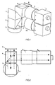
Fig.1 is a schematic perspective view of the first embodiment showing a T-type imaging apparatus with two lenses for fully automatic screen printer; -
Fig.2 is the top view of the imaging apparatus shown inFig.1 ; -
Fig.3 is the front view of the imaging apparatus shown inFig.1 during operation; -
Fig.4 is the bottom view of the imaging apparatus shown inFig.1 ; -
Fig.5 is the right view of the imaging apparatus shown inFig.1 ; -
Fig.6 is the schematic view showing the structure formed of the T-type imaging apparatus with two lenses as shown inFig.1 , and the image acquiring control and processing device, along with the positioning device; and -
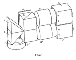
Fig.7 is a schematic perspective view of the second embodiment showing a L-type imaging apparatus with two lenses for fully automatic screen printer. - Wherein,
- 1- the first reflector;
- 2- the second reflector;
- 3- low-angle LED ring light source;
- 4- the first beamsplitter;
- 5- the second beamsplitter;
- 6- the first LED light source;
- 7- the second LED light source;
- 8- the first imaging lens;
- 9- the first image sensor;
- 10- the second imaging lens;
- 11- the second image sensor;
- 12- imaging apparatus;
- 13- screen;
- 14- printed circuit board;
- 15- positioning device;
- 16- image acquiring control and processing device;
- The above characteristics and spirit of the present invention will be more clearly understood by the detailed description of the preferred embodiments accompanying the drawings, which are given as example only without intention to limit the protection scope of the present invention.
- EMBODIMENT 1: A T-type Imaging apparatus with Two Lenses for Fully Automatic Screen Printer
- As shown in
Figs.1, 2 ,3, 4 and5 , the imaging apparatus for reference mark measurement and inspection of the solder-paste printing, includes afirst reflector 1, asecond reflector 2, a low-anglering light source 3, a first beamsplitter 4, asecond beamsplitter 5, afirstLED light source 6, a secondLED light source 7, afirst imaging lens 8, asecond imaging lens 10, aimage sensor 9 and asecond image sensor 10. The two stackedoptical reflectors LED light sources beamsplitters 4, 5. The two stackedimaging lens beamsplitters 4, 5 different from that of the optical reflectors and the light sources. The optical axes of the twostacked image sensors LED light sources LED light source 6 and the secondLED light source 7 are refracted to thefirst reflector 1 and thesecond reflector 2 by the first beamsplitter 4 and thesecond beamsplitter 5, respectively. Then, the beams of light are reflected to thescreen 13 and the printedcircuit board 14 by thefirst reflector 1 and thesecond reflector 2, respectively. The ringlight source 3 is disposed below thereflector 2, so as to provide side illumination for the printedcircuit board 14. The beam of light reflected downwards by thereflector 2 travels through the central hole of the ringlight source 3 and irradiates on the printedcircuit board 14. The reflected beams of light of thescreen 13 are reflected in an angle of 90° towards the first beamsplitter 4 by thefirst reflector 1. The reflected beams of light of the printedcircuit board 14 travel through the central hole of the ringlight source 3 and then irradiate onto thesecond reflector 2 below, by which the beams of light are reflected back to thesecond beamsplitter 5. Thefirst reflector 1 and thesecond reflector 2 are two isosceles right angle prisms stacked together. In the present embodiment, thefirst reflector 1 and thesecond reflector 2 may be two light-splitting plates or a right angle prism with two reflection planes. The first beamsplitter 4 and thesecond beamsplitter 5 are right angle prisms stacked together, or a cuboid beamsplitter, or one or two light-splitting plates. A part of the reflected light is refracted towards the firstLED light source 6 and the secondLED light source 7 by the first beamsplitter 4 and thesecond beamsplitter 5 respectively; the other part of the reflected light is reflected in an angle of 90° by the first beamsplitter 4 and thesecond beamsplitter 5 into thefirst imaging lens 8 and thesecond imaging lens 10, and then imaging is obtained on thefirst image sensor 9 and thesecond image sensor 11. Thefirst image sensor 9 and thesecond image sensor 11 may be formed of analog CCD cameras or digital CCD cameras or CMOS cameras, so that the images are converted into analog signals or digital signals by the image sensors and transferred to computer for processing. In the whole imaging apparatus, the two stacked reflectors and the two stacked light sources are disposed on two opposite sides of the two stacked beamsplitters. The imaging apparatus forms a T-shaped structure, in which the upper light path and the lower light path are independent with respect to each other, and acquire the image of the screen and the image of the printed circuit board, respectively. - As shown in
Fig. 6 , in order to cooperate with the operation of the imaging apparatus according to the present invention, an image acquiring control andprocessing device 16 and apositioning device 15 are further required. The image acquiring control andprocessing device 16 consists of a camera controller, an image acquiring card, a positioning controller, an image processing model, a general computer and a memory. The camera controller is connected to the firstLED light source 6, the secondLED light source 7, thefirst image sensor 9 and thesecond image sensor 11 respectively, and controls the image acquiring of thefirst image sensor 9 and thesecond image sensor 11. The image acquiring card is connected to the video interfaces of thefirst image sensor 9 and thesecond image sensor 11, and the image video signals are converted into digital signals. The positioning controller is connected to thepositioning device 15 on which theimaging apparatus 12 is mounted. When acquiring the images, according to the given coordinate information, theimaging apparatus 12 is conveyed to a designated position between thescreen 13 and the printedcircuit board 14. Theimaging apparatus 12 simultaneously captures the image of the screen on the side facing the printed circuit board, and the image of the printed circuit board on the side facing the screen. The image acquiring process is automatically controlled and accomplished by program. The acquired images and the processing results are stored on the memory. - When using the imaging apparatus of this embodiment, the light emitted from the first
LED light source 6 and the secondLED light source 7 is refracted towards thefirst reflector 1 and thesecond reflector 2 by the first beamsplitter 4 and thesecond beamsplitter 5. A beam of light is reflected upwards to thescreen 13 by thefirst reflector 1, while a beam of light is reflected downwards by thesecond reflector 2 and travels through the central hole of the ringlight source 3 and irradiates onto the printedcircuit board 11. The ringlight source 3 provides side illumination for the image acquiring of the printed circuit board. The beam of light reflected back from thescreen 10 is reflected towards the first beamsplitter 4 by thefirst reflector 1; the beam of light reflected back from the printedcircuit board 14 travels through the central hole of the ringlight source 3 and irradiates onto thesecond reflector 2, and then is reflected to thesecond beamsplitter 5. 50% of the light reflected back by thefirst reflector 1 and thesecond reflector 2 is refracted towards the firstLED light source 6 and the secondLED light source 7 by the first beamsplitter 4 and thesecond beamsplitter 5. The other 50% of the light is reflected in an angle of 90° towards thefirst imaging lens 8 and thesecond imaging lens 10 by the first beamsplitter 4 and thesecond beamsplitter 5, and finally the upper and lower paths of light are imaged on thefirst image sensor 9 and thesecond image sensor 10 separately. - When the apparatus according to the embodiment of the present invention is used for reference mark measurement, the images of reference marks on the printed
circuit board 14 and thescreen 13 are simultaneously acquired, and then inputted into computer after being converted into digital signals by the image acquiring card, and the coordinates of the two reference marks can be calculated, and then deviation analysis is carried out, so that the alignment in high speed and high precision can be obtained. - When the apparatus according to the embodiment of the present invention is used for the inspection of the solder paste printing, the images of the printed
circuit board 14 and thescreen 13 can be simultaneously acquired, and then inputted into computer after being converted into digital signals by the image acquiring card, and the digital signals are compared with the information of standard model stored on the computer, so that the block of the screen and the quality of solder-paste printing of the printed circuit board can be inspected. - EMBODIMENT 2: A L-type Imaging apparatus with Two Lenses for Fully Automatic Screen Printer
- As shown in
Fig. 7 , the twostacked reflectors stacked imaging lenses stacked beamsplitters 4, 5, and the two stackedLED light sources stacked beamsplitters 4, 5 different from that of the reflectors and the imaging lenses, so that the imaging apparatus forms a L-shaped structure. The other features of theembodiment 2 are the same as that of theembodiment 1 as described above. The optical axes of thefirst imaging lens 8 and thesecond imaging lens 10 are both orthogonal to that of the firstLED light source 6 and the secondLED light source 7. The angles of the light-splitting planes of the twobeamsplitters 4, 5 with respect to the axes of the twoimaging lenses LED light sources - The light emitted from the first
LED light source 6 and the secondLED light source 7 is reflected in an angle of 90°by the first beamsplitter 4 and thesecond beamsplitter 5 towards thefirst reflector 1 and thesecond reflector 2. Then, the beams of light are reflected towards thescreen 13 and the printedcircuit board 14 by thereflectors light source 3 is disposed below thereflector 2, so as to provide side illumination for the printedcircuit board 14. The beam of light reflected downwards by thereflector 2 travels through the central hole of the ringlight source 3 and irradiates onto the printedcircuit board 14. The beam of light reflected by thescreen 13 is reflected in an angle of 90° towards the first beamsplitter 4 by thefirst reflector 1. The beam of light reflected by the printedcircuit board 14 travels through the central hole of the ringlight source 3 and then irradiates onto thesecond reflector 2 below, by which the beam of light is reflected back to thesecond beamsplitter 5. Thefirst reflector 1 and thesecond reflector 2 are two isosceles right angle prisms stacked together. The reflectors also may be formed of two reflection mirror or a right angle prism with two reflection planes. A part of the reflected light from thescreen 13 or the printedcircuit board 14 is reflected in an angle of 90°by the first beamsplitter 4 and thesecond beamsplitter 5 towards the firstLED light source 6 and the secondLED light source 7; the other part of the reflected light is refracted into thefirst imaging lens 8 and thesecond imaging lens 10 by the first beamsplitter 4 and thesecond beamsplitter 5, and imaging is respectively obtained on theimage sensor 9 and theimage sensor 10. The images are converted by the image sensors into analog voltage signals or digital signals. The images are transferred to computer for processing. - The operation mode of the imaging apparatus according to this embodiment is the same as that of the
embodiment 1. - The embodiments described above are only the preferred examples without intention to limit the protection scope of the present invention. Therefore, any amendments to the structure according to the present invention as described in the specification or the drawings are within the protection scope of the present invention.
Claims (10)
- An imaging apparatus for fully automatic screen printer including two stacked light sources, two stacked beamsplitters, two stacked optical reflectors, two stacked imaging lens and two stacked image sensors, wherein the two stacked optical reflectors and the two stacked light sources are correspondingly disposed on two different sides of the two beamsplitters, the two stacked imaging lens are disposed on another side of the beamsplitters different from that of the optical reflectors and the light sources, the two stacked image sensors are disposed behind the imaging lens; the optical reflectors are provided with an upward reflection plane and a downward reflection plane, the optical axes of the imaging lenses are orthogonal to that of the light sources.
- The imaging apparatus for fully automatic screen printer according to claim1, wherein the two stacked optical reflectors and the two stacked light sources are disposed on two opposite sides of the two beamsplitters, the imaging apparatus forms a T-shaped structure.
- The imaging apparatus for fully automatic screen printer according to claim 1, wherein the two stacked optical reflectors and the stacked imaging lens are correspondingly disposed on two opposite sides of the two stacked beamsplitters, the two stacked light sources are disposed on another side of the two stacked beamsplitters different from the that of the optical reflectors and the imaging lens, the imaging apparatus forms a L-shaped structure.
- The imaging apparatus for fully automatic screen printer according to any of claims 1-3, wherein the angles of the light-splitting planes of the beamsplitters with respect to the axes of the imaging lenses and the axes of the light source are both 45°.
- The imaging apparatus for fully automatic screen printer according to any of claims 1-3, wherein the beamsplitter is formed of two right angular prisms.
- The imaging apparatus for fully automatic screen printer according to any of claims 1-3, wherein the beamsplitter is formed of one or two light-splitting plates.
- The imaging apparatus for fully automatic screen printer according to any of claims 1-3, wherein the optical reflector is formed of an isosceles right angle prism or two reflection lens or a right angle prism with two reflection planes.
- The imaging apparatus for fully automatic screen printer according to any of claims 1-3, wherein the image sensor is formed of an analog or digital CCD camera or CMOS camera.
- The imaging apparatus for fully automatic screen printer according to any of claims 1-3, wherein it further includes a ring light source, the ring light source is formed of a LED ring light source between a printed circuit board and the optical reflector in order to provide lateral illumination for the printed circuit board, the beam of light reflected downwards by the optical reflector travels through the central hole of the ring light source and then irradiates on the printed circuit board.
- The imaging apparatus for fully automatic screen printer according to any of claims 1-3, wherein the light source and the image sensor are connected to the camera controller of the image acquiring control and processing device so as to control the switching of the light source and accordingly control the image acquiring of the screen and the printed circuit board; the video signal output end of the image sensor is connected to the image acquiring card of the image acquiring control and processing device, so as to convert the acquired image video signals into digital signals.
Applications Claiming Priority (2)
| Application Number | Priority Date | Filing Date | Title |
|---|---|---|---|
| CNB2006101238949A CN100440929C (en) | 2006-11-30 | 2006-11-30 | A T-shaped double-lens image acquisition device for a fully automatic solder paste printing machine |
| CNB2006101238934A CN100421453C (en) | 2006-11-30 | 2006-11-30 | L-shaped dual-lens image acquisition device for solder paste printing |
Publications (3)
| Publication Number | Publication Date |
|---|---|
| EP1928219A2 true EP1928219A2 (en) | 2008-06-04 |
| EP1928219A3 EP1928219A3 (en) | 2009-12-30 |
| EP1928219B1 EP1928219B1 (en) | 2010-12-22 |
Family
ID=38776346
Family Applications (1)
| Application Number | Title | Priority Date | Filing Date |
|---|---|---|---|
| EP07253746A Ceased EP1928219B1 (en) | 2006-11-30 | 2007-09-21 | Imaging apparatus for fully automatic screen printer |
Country Status (4)
| Country | Link |
|---|---|
| US (3) | US8115973B2 (en) |
| EP (1) | EP1928219B1 (en) |
| CA (1) | CA2594884C (en) |
| DE (1) | DE602007011382D1 (en) |
Cited By (1)
| Publication number | Priority date | Publication date | Assignee | Title |
|---|---|---|---|---|
| EP3767937A4 (en) * | 2018-06-14 | 2021-04-14 | Guangdong Oppo Mobile Telecommunications Corp., Ltd. | CAMERA MODULE AND ELECTRONIC DEVICE |
Families Citing this family (3)
| Publication number | Priority date | Publication date | Assignee | Title |
|---|---|---|---|---|
| JP5775439B2 (en) * | 2011-12-06 | 2015-09-09 | 新電子株式会社 | Screen printing plate making inspection equipment |
| CN109927401A (en) * | 2019-01-31 | 2019-06-25 | 中国科学院西安光学精密机械研究所 | A kind of high accuracy prints machine double light path machine vision device |
| US11947094B1 (en) * | 2023-03-23 | 2024-04-02 | Illinois Tool Works Inc. | Dual camera prism assembly for stencil printer |
Family Cites Families (9)
| Publication number | Priority date | Publication date | Assignee | Title |
|---|---|---|---|---|
| JP2775921B2 (en) * | 1989-11-10 | 1998-07-16 | 松下電器産業株式会社 | Screen mask pattern hole inspection method |
| JPH07198335A (en) * | 1993-12-28 | 1995-08-01 | Omron Corp | Device and method for circumscribing position of IC chip package or print pattern |
| JPH07311025A (en) * | 1994-05-17 | 1995-11-28 | Komatsu Ltd | 3D shape inspection device |
| JPH08156224A (en) * | 1994-12-01 | 1996-06-18 | Matsushita Electric Ind Co Ltd | Screen printer |
| US6123024A (en) * | 1998-01-15 | 2000-09-26 | Alpha Metals, Inc. | Stencil incorporating electronic tag |
| JPH11245369A (en) * | 1998-02-27 | 1999-09-14 | Tenryu Seiki Kk | Image recognition device and cream solder printing device |
| US20070102477A1 (en) * | 2005-11-10 | 2007-05-10 | Speedline Technologies, Inc. | Imaging system and method for a stencil printer |
| US20070102478A1 (en) * | 2005-11-10 | 2007-05-10 | Speedline Technologies, Inc. | Optimal imaging system and method for a stencil printer |
| JP4696861B2 (en) * | 2005-11-11 | 2011-06-08 | パナソニック株式会社 | Screen printing device |
-
2007
- 2007-07-26 CA CA2594884A patent/CA2594884C/en active Active
- 2007-08-09 US US11/836,497 patent/US8115973B2/en active Active
- 2007-09-21 DE DE602007011382T patent/DE602007011382D1/en active Active
- 2007-09-21 EP EP07253746A patent/EP1928219B1/en not_active Ceased
-
2011
- 2011-04-22 US US13/092,677 patent/US20120098956A1/en not_active Abandoned
- 2011-06-07 US US13/155,036 patent/US20110234870A1/en not_active Abandoned
Cited By (2)
| Publication number | Priority date | Publication date | Assignee | Title |
|---|---|---|---|---|
| EP3767937A4 (en) * | 2018-06-14 | 2021-04-14 | Guangdong Oppo Mobile Telecommunications Corp., Ltd. | CAMERA MODULE AND ELECTRONIC DEVICE |
| US11463568B2 (en) | 2018-06-14 | 2022-10-04 | Guangdong Oppo Mobile Telecommunications Corp., Ltd. | Camera module and electronic device |
Also Published As
| Publication number | Publication date |
|---|---|
| EP1928219B1 (en) | 2010-12-22 |
| CA2594884A1 (en) | 2008-05-30 |
| HK1121904A1 (en) | 2009-04-30 |
| EP1928219A3 (en) | 2009-12-30 |
| CA2594884C (en) | 2011-12-06 |
| US20120098956A1 (en) | 2012-04-26 |
| US8115973B2 (en) | 2012-02-14 |
| US20110234870A1 (en) | 2011-09-29 |
| US20080130068A1 (en) | 2008-06-05 |
| DE602007011382D1 (en) | 2011-02-03 |
Similar Documents
| Publication | Publication Date | Title |
|---|---|---|
| KR101245148B1 (en) | Vision inspect apparatus of improved picture visibility | |
| KR101105679B1 (en) | Vision inspection device | |
| JP2014508938A (en) | Vision inspection equipment using multiple grid patterns | |
| KR101657952B1 (en) | Method of inspecting board | |
| JP4434417B2 (en) | Inspection equipment for printed wiring boards | |
| CN201058521Y (en) | Single lens image acquisition device for reference alignment and detection | |
| CN201063716Y (en) | Dual lens image capture device for fiducial alignment and detection | |
| CN101322446A (en) | Imaging system and method for a metal stencil printer | |
| KR101622628B1 (en) | Method and apparatus of inspecting a substrate with electronic devices mounted thereon | |
| EP1928219B1 (en) | Imaging apparatus for fully automatic screen printer | |
| KR101245622B1 (en) | Vision inspection apparatus using stereo vision grid pattern | |
| JPH07307599A (en) | Inspection device and product manufacturing method | |
| KR20090092116A (en) | Apparatus and method for measuring three dimension shape of a object | |
| KR101099392B1 (en) | Vision inspection device | |
| KR101123051B1 (en) | Vision inspection apparatus | |
| CN2938734Y (en) | Image collection device for reference measuring and tin paste printing detection | |
| CN100421453C (en) | L-shaped dual-lens image acquisition device for solder paste printing | |
| CN100440929C (en) | A T-shaped double-lens image acquisition device for a fully automatic solder paste printing machine | |
| HK1121904B (en) | Imaging apparatus for fully automatic screen printer | |
| CN200986617Y (en) | T-type single lens image collecting device for full-automatic tin paste printer | |
| CN200980119Y (en) | L-type dual-lens image-acquisition device for solder paste printing process | |
| CN200980120Y (en) | T-type dual-lens image-acquisition devices for full-automatic solder paste printing process machine | |
| CN1151359C (en) | Method and device for identifying the position and/or for checking the coplanarity and/or for checking the spacing of connection points of components | |
| JP2012169370A (en) | Display panel inspection equipment and display panel inspection method | |
| KR100715293B1 (en) | Vision inspection method using Hanzo's biaxial total reflection mirror |
Legal Events
| Date | Code | Title | Description |
|---|---|---|---|
| PUAI | Public reference made under article 153(3) epc to a published international application that has entered the european phase |
Free format text: ORIGINAL CODE: 0009012 |
|
| AK | Designated contracting states |
Kind code of ref document: A2 Designated state(s): AT BE BG CH CY CZ DE DK EE ES FI FR GB GR HU IE IS IT LI LT LU LV MC MT NL PL PT RO SE SI SK TR |
|
| AX | Request for extension of the european patent |
Extension state: AL BA HR MK RS |
|
| REG | Reference to a national code |
Ref country code: HK Ref legal event code: DE Ref document number: 1121904 Country of ref document: HK |
|
| PUAL | Search report despatched |
Free format text: ORIGINAL CODE: 0009013 |
|
| AK | Designated contracting states |
Kind code of ref document: A3 Designated state(s): AT BE BG CH CY CZ DE DK EE ES FI FR GB GR HU IE IS IT LI LT LU LV MC MT NL PL PT RO SE SI SK TR |
|
| AX | Request for extension of the european patent |
Extension state: AL BA HR MK RS |
|
| GRAP | Despatch of communication of intention to grant a patent |
Free format text: ORIGINAL CODE: EPIDOSNIGR1 |
|
| 17P | Request for examination filed |
Effective date: 20100329 |
|
| AKX | Designation fees paid |
Designated state(s): DE FR GB IT |
|
| GRAS | Grant fee paid |
Free format text: ORIGINAL CODE: EPIDOSNIGR3 |
|
| GRAA | (expected) grant |
Free format text: ORIGINAL CODE: 0009210 |
|
| AK | Designated contracting states |
Kind code of ref document: B1 Designated state(s): DE FR GB IT |
|
| REG | Reference to a national code |
Ref country code: GB Ref legal event code: FG4D |
|
| REF | Corresponds to: |
Ref document number: 602007011382 Country of ref document: DE Date of ref document: 20110203 Kind code of ref document: P |
|
| REG | Reference to a national code |
Ref country code: DE Ref legal event code: R096 Ref document number: 602007011382 Country of ref document: DE Effective date: 20110203 |
|
| REG | Reference to a national code |
Ref country code: HK Ref legal event code: GR Ref document number: 1121904 Country of ref document: HK |
|
| PLBE | No opposition filed within time limit |
Free format text: ORIGINAL CODE: 0009261 |
|
| STAA | Information on the status of an ep patent application or granted ep patent |
Free format text: STATUS: NO OPPOSITION FILED WITHIN TIME LIMIT |
|
| 26N | No opposition filed |
Effective date: 20110923 |
|
| REG | Reference to a national code |
Ref country code: DE Ref legal event code: R097 Ref document number: 602007011382 Country of ref document: DE Effective date: 20110923 |
|
| PG25 | Lapsed in a contracting state [announced via postgrant information from national office to epo] |
Ref country code: FR Free format text: LAPSE BECAUSE OF NON-PAYMENT OF DUE FEES Effective date: 20101222 |
|
| P01 | Opt-out of the competence of the unified patent court (upc) registered |
Effective date: 20230530 |
|
| PGFP | Annual fee paid to national office [announced via postgrant information from national office to epo] |
Ref country code: GB Payment date: 20230920 Year of fee payment: 17 |
|
| PGFP | Annual fee paid to national office [announced via postgrant information from national office to epo] |
Ref country code: DE Payment date: 20230920 Year of fee payment: 17 |
|
| PGFP | Annual fee paid to national office [announced via postgrant information from national office to epo] |
Ref country code: IT Payment date: 20230927 Year of fee payment: 17 |
|
| REG | Reference to a national code |
Ref country code: DE Ref legal event code: R119 Ref document number: 602007011382 Country of ref document: DE |
|
| GBPC | Gb: european patent ceased through non-payment of renewal fee |
Effective date: 20240921 |
|
| PG25 | Lapsed in a contracting state [announced via postgrant information from national office to epo] |
Ref country code: DE Free format text: LAPSE BECAUSE OF NON-PAYMENT OF DUE FEES Effective date: 20250401 |
|
| PG25 | Lapsed in a contracting state [announced via postgrant information from national office to epo] |
Ref country code: GB Free format text: LAPSE BECAUSE OF NON-PAYMENT OF DUE FEES Effective date: 20240921 |
|
| PG25 | Lapsed in a contracting state [announced via postgrant information from national office to epo] |
Ref country code: IT Free format text: LAPSE BECAUSE OF NON-PAYMENT OF DUE FEES Effective date: 20240921 |