EP1928005A2 - Commutation sans arc basé sur un système micro-électromécanique avec circuit pour absorber une alimentation électrique au cours d'une condition de panne - Google Patents
Commutation sans arc basé sur un système micro-électromécanique avec circuit pour absorber une alimentation électrique au cours d'une condition de panne Download PDFInfo
- Publication number
- EP1928005A2 EP1928005A2 EP07110553A EP07110553A EP1928005A2 EP 1928005 A2 EP1928005 A2 EP 1928005A2 EP 07110553 A EP07110553 A EP 07110553A EP 07110553 A EP07110553 A EP 07110553A EP 1928005 A2 EP1928005 A2 EP 1928005A2
- Authority
- EP
- European Patent Office
- Prior art keywords
- pulse
- circuit
- switch
- current
- energy
- Prior art date
- Legal status (The legal status is an assumption and is not a legal conclusion. Google has not performed a legal analysis and makes no representation as to the accuracy of the status listed.)
- Granted
Links
- 230000004044 response Effects 0.000 claims abstract description 26
- 230000015572 biosynthetic process Effects 0.000 claims abstract description 11
- 239000003990 capacitor Substances 0.000 claims description 56
- 230000000452 restraining effect Effects 0.000 claims description 2
- 238000000034 method Methods 0.000 description 23
- 230000001629 suppression Effects 0.000 description 18
- 238000010586 diagram Methods 0.000 description 15
- 230000008569 process Effects 0.000 description 10
- 230000007423 decrease Effects 0.000 description 9
- 238000001514 detection method Methods 0.000 description 8
- 230000006870 function Effects 0.000 description 7
- 230000002441 reversible effect Effects 0.000 description 6
- 230000009471 action Effects 0.000 description 5
- 238000012546 transfer Methods 0.000 description 5
- 230000001419 dependent effect Effects 0.000 description 4
- 230000000977 initiatory effect Effects 0.000 description 4
- 238000005457 optimization Methods 0.000 description 4
- 230000009467 reduction Effects 0.000 description 4
- 230000002829 reductive effect Effects 0.000 description 4
- 238000000926 separation method Methods 0.000 description 4
- 230000001960 triggered effect Effects 0.000 description 4
- 239000013598 vector Substances 0.000 description 4
- 230000003466 anti-cipated effect Effects 0.000 description 3
- 230000008859 change Effects 0.000 description 3
- 230000003247 decreasing effect Effects 0.000 description 3
- 238000013461 design Methods 0.000 description 2
- 230000007246 mechanism Effects 0.000 description 2
- 238000012986 modification Methods 0.000 description 2
- 230000004048 modification Effects 0.000 description 2
- 230000003071 parasitic effect Effects 0.000 description 2
- 230000001681 protective effect Effects 0.000 description 2
- 230000001052 transient effect Effects 0.000 description 2
- 238000010521 absorption reaction Methods 0.000 description 1
- 238000013459 approach Methods 0.000 description 1
- 230000008901 benefit Effects 0.000 description 1
- 230000000903 blocking effect Effects 0.000 description 1
- 239000002131 composite material Substances 0.000 description 1
- 238000013016 damping Methods 0.000 description 1
- 238000012938 design process Methods 0.000 description 1
- 230000001627 detrimental effect Effects 0.000 description 1
- 230000003467 diminishing effect Effects 0.000 description 1
- 230000000694 effects Effects 0.000 description 1
- 238000005516 engineering process Methods 0.000 description 1
- 230000006872 improvement Effects 0.000 description 1
- 230000001939 inductive effect Effects 0.000 description 1
- 230000005764 inhibitory process Effects 0.000 description 1
- 230000003993 interaction Effects 0.000 description 1
- 230000000670 limiting effect Effects 0.000 description 1
- 238000004519 manufacturing process Methods 0.000 description 1
- 229910044991 metal oxide Inorganic materials 0.000 description 1
- 150000004706 metal oxides Chemical class 0.000 description 1
- 238000012544 monitoring process Methods 0.000 description 1
- 238000004806 packaging method and process Methods 0.000 description 1
- 230000021715 photosynthesis, light harvesting Effects 0.000 description 1
- 238000012163 sequencing technique Methods 0.000 description 1
- 238000007493 shaping process Methods 0.000 description 1
- 238000004088 simulation Methods 0.000 description 1
- 230000003068 static effect Effects 0.000 description 1
- 239000000758 substrate Substances 0.000 description 1
Images


Classifications
-
- H—ELECTRICITY
- H01—ELECTRIC ELEMENTS
- H01H—ELECTRIC SWITCHES; RELAYS; SELECTORS; EMERGENCY PROTECTIVE DEVICES
- H01H59/00—Electrostatic relays; Electro-adhesion relays
- H01H59/0009—Electrostatic relays; Electro-adhesion relays making use of micromechanics
-
- H—ELECTRICITY
- H01—ELECTRIC ELEMENTS
- H01H—ELECTRIC SWITCHES; RELAYS; SELECTORS; EMERGENCY PROTECTIVE DEVICES
- H01H9/00—Details of switching devices, not covered by groups H01H1/00 - H01H7/00
- H01H9/54—Circuit arrangements not adapted to a particular application of the switching device and for which no provision exists elsewhere
- H01H9/541—Contacts shunted by semiconductor devices
- H01H9/542—Contacts shunted by static switch means
- H01H2009/543—Contacts shunted by static switch means third parallel branch comprising an energy absorber, e.g. MOV, PTC, Zener
-
- H—ELECTRICITY
- H01—ELECTRIC ELEMENTS
- H01H—ELECTRIC SWITCHES; RELAYS; SELECTORS; EMERGENCY PROTECTIVE DEVICES
- H01H71/00—Details of the protective switches or relays covered by groups H01H73/00 - H01H83/00
- H01H2071/008—Protective switches or relays using micromechanics
-
- H—ELECTRICITY
- H01—ELECTRIC ELEMENTS
- H01H—ELECTRIC SWITCHES; RELAYS; SELECTORS; EMERGENCY PROTECTIVE DEVICES
- H01H9/00—Details of switching devices, not covered by groups H01H1/00 - H01H7/00
- H01H9/54—Circuit arrangements not adapted to a particular application of the switching device and for which no provision exists elsewhere
- H01H9/541—Contacts shunted by semiconductor devices
-
- H—ELECTRICITY
- H03—ELECTRONIC CIRCUITRY
- H03K—PULSE TECHNIQUE
- H03K17/00—Electronic switching or gating, i.e. not by contact-making and –breaking
- H03K17/08—Modifications for protecting switching circuit against overcurrent or overvoltage
- H03K17/081—Modifications for protecting switching circuit against overcurrent or overvoltage without feedback from the output circuit to the control circuit
- H03K17/0814—Modifications for protecting switching circuit against overcurrent or overvoltage without feedback from the output circuit to the control circuit by measures taken in the output circuit
- H03K17/08142—Modifications for protecting switching circuit against overcurrent or overvoltage without feedback from the output circuit to the control circuit by measures taken in the output circuit in field-effect transistor switches
-
- H—ELECTRICITY
- H03—ELECTRONIC CIRCUITRY
- H03K—PULSE TECHNIQUE
- H03K17/00—Electronic switching or gating, i.e. not by contact-making and –breaking
- H03K17/08—Modifications for protecting switching circuit against overcurrent or overvoltage
- H03K17/082—Modifications for protecting switching circuit against overcurrent or overvoltage by feedback from the output to the control circuit
- H03K17/0822—Modifications for protecting switching circuit against overcurrent or overvoltage by feedback from the output to the control circuit in field-effect transistor switches
Definitions
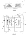
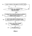
- the system includes switching circuitry comprising a micro-electromechanical system switch configured to switch the system from a first switching state to a second switching state.
- An arc suppression circuitry is coupled to the switching circuitry, wherein the arc suppression circuitry is configured to suppress an arc formation between contacts of the micro-electromechanical system switch.
- Detection circuitry is coupled to the arc suppression circuitry and configured to determine existence of a fault condition.
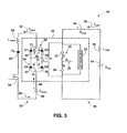
- the first MEMS switch 20 may be coupled in parallel across midpoints of the balanced diode bridge 28.
- the midpoints of the balanced diode bridge may include a first midpoint located between the first and second diodes 30, 32 and a second midpoint located between the third and fourth diodes 34, 36.
- the first MEMS switch 20 and the balanced diode bridge 28 may be tightly packaged to facilitate minimization of parasitic inductance caused by the balanced diode bridge 28 and in particular, the connections to the MEMS switch 20.
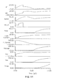
- the pulse circuit 52 may include a pulse switch 54 and a pulse capacitor C PULSE 56 series coupled to the pulse switch 54. Further, the pulse circuit may also include a pulse inductance L PULSE 58 and a first diode D P 60 coupled in series with the pulse switch 54. The pulse inductance L PULSE 58, the diode D P 60, the pulse switch 54 and the pulse capacitor C PULSE 56 may be coupled in series to form a first branch of the pulse circuit 52, where the components of the first branch may be configured to facilitate pulse current shaping and timing. Also, reference numeral 62 is representative of a pulse circuit current I PULSE that may flow through the pulse circuit 52.
- triggering of the pulse switch 54 may include controlling a timing of the pulse circuit current I PULSE 62 through the balanced diode bridge 28 to facilitate creating a lower impedance path as compared to the impedance of a path through the contacts of the MEMS switch 20 during an opening interval.
- the pulse switch 54 may be triggered such that a desired voltage drop is presented across the contacts of the MEMS switch 20.
- the pulse switch 54 may be a solid-state switch that may be configured to have switching speeds in the range of nanoseconds to microseconds, for example.
- the switching speed of the pulse switch 54 should be relatively fast compared to the anticipated rise time of the load current in a fault condition.
- the current rating of the MEMS switch 20 is dependent on the rate of rise of the load current, which in turn is dependent on the inductance L LOAD 46 and the bus supply voltage V BUS 44 in the load circuit 40 as previously noted.
- the MEMS switch 20 may be appropriately rated to handle a larger load current I LOAD 50 if the load current
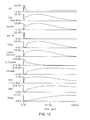
- the pulse circuit current I PULSE 62 may resonantly decrease to a zero value and to maintain the zero value due to the reverse blocking action of the diode bridge 28 and the diode D P 60.
- a circuit arrangement embodying aspects of the present invention should result in a reduced amount of fault let-through current and lower breaker energy dissipation.
- diode bridge 28 and MEMS switch 20 may be packaged to be closely integrated with one another (e.g., composite packaging) for reduction of parasitic inductance in the diode bridge and the respective interconnections to the MEMS switch. This incrementally reduces the amount of electrical energy that may be stored in such interconnections.
Landscapes
- Electronic Switches (AREA)
- Driving Mechanisms And Operating Circuits Of Arc-Extinguishing High-Tension Switches (AREA)
- Arc Welding Control (AREA)
- Keying Circuit Devices (AREA)
Applications Claiming Priority (1)
| Application Number | Priority Date | Filing Date | Title |
|---|---|---|---|
| US11/563,726 US7876538B2 (en) | 2005-12-20 | 2006-11-28 | Micro-electromechanical system based arc-less switching with circuitry for absorbing electrical energy during a fault condition |
Publications (3)
| Publication Number | Publication Date |
|---|---|
| EP1928005A2 true EP1928005A2 (fr) | 2008-06-04 |
| EP1928005A3 EP1928005A3 (fr) | 2009-07-15 |
| EP1928005B1 EP1928005B1 (fr) | 2013-09-25 |
Family
ID=39083243
Family Applications (1)
| Application Number | Title | Priority Date | Filing Date |
|---|---|---|---|
| EP07110553.0A Active EP1928005B1 (fr) | 2006-11-28 | 2007-06-19 | Commutation sans arc basé sur un système micro-électromécanique avec circuit pour absorber une alimentation électrique au cours d'une condition de panne |
Country Status (5)
| Country | Link |
|---|---|
| US (2) | US7876538B2 (fr) |
| EP (1) | EP1928005B1 (fr) |
| JP (1) | JP5202882B2 (fr) |
| CN (1) | CN101192477B (fr) |
| MX (1) | MX2007014897A (fr) |
Cited By (1)
| Publication number | Priority date | Publication date | Assignee | Title |
|---|---|---|---|---|
| US9087653B2 (en) | 2010-03-12 | 2015-07-21 | Arc Suppression Technologies, Llc | Two terminal arc suppressor |
Families Citing this family (20)
| Publication number | Priority date | Publication date | Assignee | Title |
|---|---|---|---|---|
| US7876538B2 (en) * | 2005-12-20 | 2011-01-25 | General Electric Company | Micro-electromechanical system based arc-less switching with circuitry for absorbing electrical energy during a fault condition |
| US9076607B2 (en) * | 2007-01-10 | 2015-07-07 | General Electric Company | System with circuitry for suppressing arc formation in micro-electromechanical system based switch |
| US7542250B2 (en) * | 2007-01-10 | 2009-06-02 | General Electric Company | Micro-electromechanical system based electric motor starter |
| US8358488B2 (en) * | 2007-06-15 | 2013-01-22 | General Electric Company | Micro-electromechanical system based switching |
| US7554222B2 (en) * | 2007-11-01 | 2009-06-30 | General Electric Company | Micro-electromechanical system based switching |
| IL194955A0 (en) * | 2008-10-28 | 2009-08-03 | Alexsander Ulanovsky | Solid state device for voltage decreasing for the electric circuit of direct and alternating current of medium and high voltage |
| US8427792B2 (en) * | 2009-05-29 | 2013-04-23 | General Electric Company | Method and system to enhance reliability of switch array |
| US8203319B2 (en) * | 2009-07-09 | 2012-06-19 | General Electric Company | Transformer on-load tap changer using MEMS technology |
| US8916995B2 (en) * | 2009-12-02 | 2014-12-23 | General Electric Company | Method and apparatus for switching electrical power |
| EP2518745A3 (fr) * | 2011-04-28 | 2013-04-24 | General Electric Company | Réseau de commutation comprenant des circuits pour ajuster une distribution temporelle d'un signal de déclenchement appliqué au réseau |
| US20130027817A1 (en) * | 2011-07-25 | 2013-01-31 | General Electric Company | Micro electro-mechanical switch (mems) based over current motor protection system |
| US8773235B2 (en) | 2011-11-30 | 2014-07-08 | General Electric Company | Electrical switch and circuit breaker |
| US8659326B1 (en) | 2012-09-28 | 2014-02-25 | General Electric Company | Switching apparatus including gating circuitry for actuating micro-electromechanical system (MEMS) switches |
| US20140091808A1 (en) * | 2012-09-28 | 2014-04-03 | Arc Suppression Technologies | Contact separation detector and methods therefor |
| US10068733B2 (en) | 2015-10-22 | 2018-09-04 | General Electric Company | Micro-electromechanical system relay circuit |
| US10083811B2 (en) * | 2015-10-22 | 2018-09-25 | General Electric Company | Auxiliary circuit for micro-electromechanical system relay circuit |
| US10211622B2 (en) | 2016-06-29 | 2019-02-19 | General Electric Company | System and method for fault interruption with MEMS switches |
| DE112017007451T5 (de) * | 2017-04-18 | 2020-02-20 | Mitsubishi Electric Corporation | Überstrom-erfassungsschaltung und leistungswandler |
| GB2569185A (en) | 2017-12-11 | 2019-06-12 | Eaton Intelligent Power Ltd | Fault clearing circuitry |
| US11114257B2 (en) * | 2018-04-06 | 2021-09-07 | Yazaki North America, Inc. | Methods and apparatus for DC arc detection/suppression |
Family Cites Families (16)
| Publication number | Priority date | Publication date | Assignee | Title |
|---|---|---|---|---|
| US4500934A (en) | 1982-06-21 | 1985-02-19 | General Electric Company | Hybrid switching device employing liquid metal contact |
| US4700256A (en) | 1984-05-16 | 1987-10-13 | General Electric Company | Solid state current limiting circuit interrupter |
| JPS61259416A (ja) * | 1985-05-10 | 1986-11-17 | 大光電気株式会社 | スイツチ回路 |
| US4723187A (en) | 1986-11-10 | 1988-02-02 | General Electric Company | Current commutation circuit |
| EP0272349B1 (fr) | 1986-12-22 | 1993-05-19 | S.A. Acec Transport | Disjoncteur hyper rapide assisté par semi-conducteurs |
| US5339210A (en) * | 1992-07-22 | 1994-08-16 | General Electric Company | DC circuit interrupter |
| US5430597A (en) | 1993-01-04 | 1995-07-04 | General Electric Company | Current interrupting device using micromechanical components |
| US5374792A (en) * | 1993-01-04 | 1994-12-20 | General Electric Company | Micromechanical moving structures including multiple contact switching system |
| DE19846639A1 (de) | 1998-10-09 | 2000-04-27 | Abb Research Ltd | Neue elektrische Schalteinrichtung |
| SE9900852D0 (sv) | 1999-03-08 | 1999-03-08 | Secheron Sa | An electrical coil module, an electrical coil comprising such modules, an actuation mechanism including such a coil and a circuit breaker comprising such an actuation mechanism |
| DE19927762A1 (de) | 1999-06-17 | 2001-01-04 | Abb Research Ltd | Neue elektrische Schalteinrichtung zum Überstromschutz |
| US6952335B2 (en) | 2002-03-22 | 2005-10-04 | Virginia Tech Intellectual Properties, Inc. | Solid-state DC circuit breaker |
| GB2387480B (en) | 2002-04-09 | 2005-04-13 | Microsaic Systems Ltd | Micro-engineered self-releasing switch |
| ES2259409T3 (es) | 2003-12-05 | 2006-10-01 | Societe Technique Pour L'energie Atomique Technicatome | Dispositivo disyuntor hibrido. |
| US6884950B1 (en) * | 2004-09-15 | 2005-04-26 | Agilent Technologies, Inc. | MEMs switching system |
| US7876538B2 (en) * | 2005-12-20 | 2011-01-25 | General Electric Company | Micro-electromechanical system based arc-less switching with circuitry for absorbing electrical energy during a fault condition |
-
2006
- 2006-11-28 US US11/563,726 patent/US7876538B2/en active Active
-
2007
- 2007-06-19 EP EP07110553.0A patent/EP1928005B1/fr active Active
- 2007-06-25 JP JP2007165724A patent/JP5202882B2/ja active Active
- 2007-07-02 CN CN2007101273307A patent/CN101192477B/zh not_active Expired - Fee Related
- 2007-11-27 MX MX2007014897A patent/MX2007014897A/es active IP Right Grant
-
2010
- 2010-12-14 US US12/967,526 patent/US8050000B2/en active Active
Non-Patent Citations (1)
| Title |
|---|
| None |
Cited By (6)
| Publication number | Priority date | Publication date | Assignee | Title |
|---|---|---|---|---|
| US9087653B2 (en) | 2010-03-12 | 2015-07-21 | Arc Suppression Technologies, Llc | Two terminal arc suppressor |
| US9508501B2 (en) | 2010-03-12 | 2016-11-29 | Arc Suppression Technologies, Llc | Two terminal arc suppressor |
| US10134536B2 (en) | 2010-03-12 | 2018-11-20 | Arc Suppression Technologies, Llc | Two terminal arc suppressor |
| US10748719B2 (en) | 2010-03-12 | 2020-08-18 | Arc Suppression Technologies, Llc | Two terminal arc suppressor |
| US11295906B2 (en) | 2010-03-12 | 2022-04-05 | Arc Suppression Technologies, Llc | Two terminal arc suppressor |
| US11676777B2 (en) | 2010-03-12 | 2023-06-13 | Arc Suppression Technologies, Llc | Two terminal arc suppressor |
Also Published As
| Publication number | Publication date |
|---|---|
| US20110096444A1 (en) | 2011-04-28 |
| US8050000B2 (en) | 2011-11-01 |
| CN101192477A (zh) | 2008-06-04 |
| JP2008211755A (ja) | 2008-09-11 |
| US7876538B2 (en) | 2011-01-25 |
| US20070139831A1 (en) | 2007-06-21 |
| EP1928005B1 (fr) | 2013-09-25 |
| CN101192477B (zh) | 2012-10-10 |
| EP1928005A3 (fr) | 2009-07-15 |
| MX2007014897A (es) | 2009-02-19 |
| JP5202882B2 (ja) | 2013-06-05 |
Similar Documents
| Publication | Publication Date | Title |
|---|---|---|
| EP1928005B1 (fr) | Commutation sans arc basé sur un système micro-électromécanique avec circuit pour absorber une alimentation électrique au cours d'une condition de panne | |
| EP1930922B1 (fr) | Circuit de commutation électromécanique en parallèle avec un circuit de commutation semi-conducteur pouvant être commutés sélectivement pour porter un courant de charge approprié pour un tel circuit | |
| US7542250B2 (en) | Micro-electromechanical system based electric motor starter | |
| US8054589B2 (en) | Switch structure and associated circuit | |
| KR101468743B1 (ko) | 마이크로 전기기계 시스템 기반 스위치 내 아크 형성을 억제하는 회로를 구비한 시스템 | |
| US8358488B2 (en) | Micro-electromechanical system based switching | |
| US20070139829A1 (en) | Micro-electromechanical system based arc-less switching | |
| US7633725B2 (en) | Micro-electromechanical system based soft switching | |
| EP2056325B1 (fr) | Système et procédé pour éviter le frottement de contact dans un commutateur basé sur un système micro-électromécanique | |
| KR101445386B1 (ko) | 마이크로-전자기계적 시스템 스위치 및 밸런싱된 다이오드브릿지를 포함하는 시스템 | |
| EP2017870B1 (fr) | Commutation souple basée sur un système micro-électromécanique |
Legal Events
| Date | Code | Title | Description |
|---|---|---|---|
| PUAI | Public reference made under article 153(3) epc to a published international application that has entered the european phase |
Free format text: ORIGINAL CODE: 0009012 |
|
| AK | Designated contracting states |
Kind code of ref document: A2 Designated state(s): AT BE BG CH CY CZ DE DK EE ES FI FR GB GR HU IE IS IT LI LT LU LV MC MT NL PL PT RO SE SI SK TR |
|
| AX | Request for extension of the european patent |
Extension state: AL BA HR MK RS |
|
| PUAL | Search report despatched |
Free format text: ORIGINAL CODE: 0009013 |
|
| AK | Designated contracting states |
Kind code of ref document: A3 Designated state(s): AT BE BG CH CY CZ DE DK EE ES FI FR GB GR HU IE IS IT LI LT LU LV MC MT NL PL PT RO SE SI SK TR |
|
| AX | Request for extension of the european patent |
Extension state: AL BA HR MK RS |
|
| 17P | Request for examination filed |
Effective date: 20100115 |
|
| AKX | Designation fees paid |
Designated state(s): DE FR GB IT |
|
| 17Q | First examination report despatched |
Effective date: 20100315 |
|
| GRAP | Despatch of communication of intention to grant a patent |
Free format text: ORIGINAL CODE: EPIDOSNIGR1 |
|
| INTG | Intention to grant announced |
Effective date: 20130425 |
|
| GRAS | Grant fee paid |
Free format text: ORIGINAL CODE: EPIDOSNIGR3 |
|
| GRAA | (expected) grant |
Free format text: ORIGINAL CODE: 0009210 |
|
| AK | Designated contracting states |
Kind code of ref document: B1 Designated state(s): DE FR GB IT |
|
| REG | Reference to a national code |
Ref country code: GB Ref legal event code: FG4D |
|
| REG | Reference to a national code |
Ref country code: DE Ref legal event code: R096 Ref document number: 602007033006 Country of ref document: DE Effective date: 20131121 |
|
| REG | Reference to a national code |
Ref country code: DE Ref legal event code: R097 Ref document number: 602007033006 Country of ref document: DE |
|
| PLBE | No opposition filed within time limit |
Free format text: ORIGINAL CODE: 0009261 |
|
| STAA | Information on the status of an ep patent application or granted ep patent |
Free format text: STATUS: NO OPPOSITION FILED WITHIN TIME LIMIT |
|
| 26N | No opposition filed |
Effective date: 20140626 |
|
| REG | Reference to a national code |
Ref country code: DE Ref legal event code: R097 Ref document number: 602007033006 Country of ref document: DE Effective date: 20140626 |
|
| REG | Reference to a national code |
Ref country code: DE Ref legal event code: R119 Ref document number: 602007033006 Country of ref document: DE |
|
| GBPC | Gb: european patent ceased through non-payment of renewal fee |
Effective date: 20140619 |
|
| REG | Reference to a national code |
Ref country code: DE Ref legal event code: R119 Ref document number: 602007033006 Country of ref document: DE Effective date: 20150101 |
|
| PG25 | Lapsed in a contracting state [announced via postgrant information from national office to epo] |
Ref country code: DE Free format text: LAPSE BECAUSE OF NON-PAYMENT OF DUE FEES Effective date: 20150101 Ref country code: IT Free format text: LAPSE BECAUSE OF NON-PAYMENT OF DUE FEES Effective date: 20140619 |
|
| PG25 | Lapsed in a contracting state [announced via postgrant information from national office to epo] |
Ref country code: GB Free format text: LAPSE BECAUSE OF NON-PAYMENT OF DUE FEES Effective date: 20140619 |
|
| REG | Reference to a national code |
Ref country code: FR Ref legal event code: PLFP Year of fee payment: 10 |
|
| REG | Reference to a national code |
Ref country code: FR Ref legal event code: PLFP Year of fee payment: 11 |
|
| REG | Reference to a national code |
Ref country code: FR Ref legal event code: PLFP Year of fee payment: 12 |
|
| PGFP | Annual fee paid to national office [announced via postgrant information from national office to epo] |
Ref country code: FR Payment date: 20240522 Year of fee payment: 18 |