EP1927154B1 - Compact multilayer circuit - Google Patents
Compact multilayer circuit Download PDFInfo
- Publication number
- EP1927154B1 EP1927154B1 EP06789897A EP06789897A EP1927154B1 EP 1927154 B1 EP1927154 B1 EP 1927154B1 EP 06789897 A EP06789897 A EP 06789897A EP 06789897 A EP06789897 A EP 06789897A EP 1927154 B1 EP1927154 B1 EP 1927154B1
- Authority
- EP
- European Patent Office
- Prior art keywords
- input
- layer
- switching network
- output
- groundplane
- Prior art date
- Legal status (The legal status is an assumption and is not a legal conclusion. Google has not performed a legal analysis and makes no representation as to the accuracy of the status listed.)
- Not-in-force
Links
Images

Classifications
-
- H—ELECTRICITY
- H01—ELECTRIC ELEMENTS
- H01P—WAVEGUIDES; RESONATORS, LINES, OR OTHER DEVICES OF THE WAVEGUIDE TYPE
- H01P1/00—Auxiliary devices
- H01P1/20—Frequency-selective devices, e.g. filters
- H01P1/201—Filters for transverse electromagnetic waves
- H01P1/203—Strip line filters
-
- H—ELECTRICITY
- H01—ELECTRIC ELEMENTS
- H01P—WAVEGUIDES; RESONATORS, LINES, OR OTHER DEVICES OF THE WAVEGUIDE TYPE
- H01P1/00—Auxiliary devices
- H01P1/20—Frequency-selective devices, e.g. filters
- H01P1/201—Filters for transverse electromagnetic waves
- H01P1/203—Strip line filters
- H01P1/20327—Electromagnetic interstage coupling
- H01P1/20336—Comb or interdigital filters
- H01P1/20345—Multilayer filters
-
- H—ELECTRICITY
- H01—ELECTRIC ELEMENTS
- H01P—WAVEGUIDES; RESONATORS, LINES, OR OTHER DEVICES OF THE WAVEGUIDE TYPE
- H01P1/00—Auxiliary devices
- H01P1/10—Auxiliary devices for switching or interrupting
- H01P1/12—Auxiliary devices for switching or interrupting by mechanical chopper
- H01P1/127—Strip line switches
Definitions
- This invention relates to circuits. Specifically, the present invention relates to systems and methods for packaging and isolating circuits, such as microwave frequency converter circuits.
- Circuit isolation and packaging systems are employed in various demanding applications including microwave filter banks. Such applications demand compact packaging that minimizes electrical interference between components.
- microwave frequency-shifter components are individually packaged in expensive double-sided cavitized housing assemblies, which are interconnected via wire, ribbon, and/or solder interconnects. Such component assemblies are often undesirably large and expensive. Furthermore, the various interconnects are prone to breakage, which reduces system reliability.
- the system is adapted for use with microwave signals.
- the system includes a first mechanism for receiving an input signal and selectively routing the input signal onto a first signal path.
- a second mechanism routes the input signal along the first signal path through one or more layers, including one or more groundplane layers, to a first circuit component for modifying the input signal and providing an adjusted signal in response thereto.
- a third mechanism outputs the adjusted signal.
- a multilayer signal processing system comprising a first mechanism for receiving an input signal and selectively routing the input signal onto a first signal path; a second mechanism for routing the input signal along the first signal path vertically through one or more horizontal layers to a first circuit component that provides an adjusted signal in response to receipt of the input signal; and a third mechanism for outputting the adjusted signal, wherein the one or more horizontal layers include one or more ground plane layers, and wherein the first mechanism includes an input switching network in communication with one or more controllers for selectively switching the input signal onto one of plural input signal paths, the switching network disposed on a switching layer, wherein the second mechanism further includes a first input waveguide extending from the input switching network vertically through at least one groundplane layer and to an input end of the first circuit component, wherein the third mechanism includes a first output waveguide extending from an output end of the first circuit component and vertically through the at least one groundplane layer and to an output switching network disposed on the switching layer, and wherein the input switching network and the output
- the circuit layer includes plural circuit components, each coupled to a respective input waveguide and output waveguide that extend vertically through the first groundplane layer to the input switching network and the output switching network, respectively, wherein the system further includes one or more controllers coupled to the input switching network and/or to the output switching network and adapted to selectively activate or select a desired circuit component disposed on the circuit layer in response to a given operational mode of the multilayer signal processing system, wherein the system further includes one or more additional circuit layers disposed substantially adjacent to and parallel to the second groundplane layer on a side of the second groundplane layer opposite the circuit layer, and wherein the one or more additional circuit layers include one or more additional microwave filters disposed therein or thereon, and wherein the first input waveguide and the first output waveguide are equipped with parallel mode-suppression holes, the first input waveguide and the first output waveguide being circular waveguides.
- the first circuit component is a microwave filter.
- the circuit layer includes plural circuit components that are each coupled to a respective input waveguide and output waveguide that extend through the first groundplane layer to the input switching network and the output switching network, respectively.
- the system further includes one or more controllers coupled to the input switching network and/or to the output switching network.
- the one or more controllers are adapted to selectively activate or select a desired circuit component disposed on the circuit layer in response to a given operational mode of the multilayer signal processing system.
- the system further includes one or more additional circuit layers disposed substantially adjacent to and parallel to the second groundplane layer on a side of the second groundplane layer opposite the circuit layer.
- the one or more additional circuit layers include one or more additional microwave filters disposed therein.
- the various waveguides, including the first input waveguide and the first output waveguide are equipped with mode-suppression holes that parallel the waveguides, which are circular waveguides.
- One embodiment of the present invention is a stacked multilayer microwave filter with several filter elements.
- the unique positioning of the filter elements between or adjacent to groundplanes facilitates improved input/output isolation and significantly reduces the form factor required to implement the filter.
- Versatility and scalability of the filter is enhanced via use of unique input and output switching networks.
- the switching networks can switch a filter input signal to an appropriate layer and accompanying filter element and then selectively output the resulting filtered output signal while achieving minimal interference and maximum electrical isolation between filter input and output terminals.
- the vertical waveguides that couple the filter elements to the switching networks and that extend through one or more layers of the filter are equipped with special mode-suppression holes that further enhance filter response characteristics.
- Fig. 1 is an exploded view of a stacked multilayer programmable microwave filter 10 according to an embodiment of the present invention.
- various well-known components such as power supplies, antennas, and so on, have been omitted from the figures.
- those skilled in the art with access to the present teachings will know which components to implement and how to implement them to meet the needs of a given application.
- the stacked programmable microwave filter 10 includes, from top to bottom, a switching layer 14, a control-routing layer 16, a first groundplane layer 18, a first filter layer 20, a second groundplane layer 22, and a second filter layer 24.
- the various layers 14-24 are approximately parallel and coincident as shown in Fig. 1 .
- the various layers 14-24 have a low-loss dielectric substrate core, which in the present embodiment is Duroid. Duroid may be ordered from Rogers Corp.
- the switching layer 14 includes an input switching network 24 and an output switching network 26, which are positioned on opposite ends of a top surface 48 of the switching layer 14.
- the switching networks 24, 26 are implemented via microstrip with a common groundplane implemented via the first groundplane layer 18.
- the input switching network 24 includes an input terminal 28 for receiving an input microwave signal.
- the input terminal 28 connects to an input of a first 1-4 switch 30.
- the first 1-4 switch 30 selectively provides input to a second 1-4 switch 32, a first vertical RF transition 34, a second vertical RF transition 36, and a third 1-4 switch 38.
- the second 1-4 switch 32 selectively provides input to a third vertical RF transition 50, a fourth vertical RF transition 52, a fifth vertical RF transition 54, and a sixth vertical RF transition 56.
- the third 1-4 switch 38 selectively provides input to a seventh vertical RF transition 58, an eighth vertical RF transition 60, a ninth vertical RF transition 62, and a tenth vertical waveguide RF transition 64.
- the 1-4 switches 30, 32, 38 are responsive to control signals received from a first Application-Specific Integrated Circuit (ASIC) controller 40.
- the control signals are routed through the control-routing layer 16 via a first set of routing paths 42, which are connected to the first ASIC controller and to the input switching network 24 via vertical connections (not shown) extending through the switching layer 14.
- ASIC Application-Specific Integrated Circuit
- the output switching network 26 includes a first 4-1 switch 68, an output of which represents the output of the programmable stacked microwave filter 10 as provided at an output terminal 78.
- the 4-1 switch 68 In response to receipt of control signals from a second controller 44, the 4-1 switch 68 selectively switches inputs from a second 4-1 switch 70, a first output vertical RF transition 72, a second output vertical RF transition 74, and a third 4-1 switch 76 to the output terminal 78.
- the second 4-1 switch 70 selectively switches input from third, fourth, fifth, and sixth output vertical RF transitions 80-86, respectively, to an input of the first 4-1 switch 68 in response to receipt of specific control signals from the second controller 44.
- the third 4-1 switch 76 selectively switches input from seventh, eighth, ninth, and tenth vertical RF transitions 88-94, respectively, to an input of the first 4-1 switch 68.
- the various switches 68, 70, 76 are responsive to control signals received from the second ASIC controller 44.
- the control signals are routed through the control-routing layer 16 via a second set of routing paths 46, which are connected to the second ASIC controller and to the output switching network 26 via vertical connections (not shown) extending through the switching layer 14.
- the first, third, fifth, seventh, and ninth input vertical RF transitions 34, 50, 54, 58, 62, respectively, extend approximately perpendicularly through the switching layer 14, the control-routing layer 16, and the first groundplane layer 18 to the first filter layer 20.
- the input vertical RF transitions 34, 50, 54, 58, 62 couple to inputs of five respective first-layer filter elements 96, three of which are visible in Fig. 1 .
- the three visible first-layer filter elements include a first filter element 98, a second filter element 100, and a third filter element 102, which are coupled to the third input vertical RF transition 50, the fifth input vertical waveguide 54, and the first input vertical waveguide 34, respectively.
- the corresponding first, third, fifth, seventh, and ninth output vertical RF transitions 72, 80, 84, 88, 92, respectively, extend approximately perpendicularly through the switching layer 14, the control-routing layer 16, and the first groundplane layer 18, and couple to outputs of the respective first-layer filter elements 96.
- Outputs of the first filter element 98, second filter element 100, and third filter element 102 are coupled to the third output vertical RF transition 80, fifth output vertical RF transition 84, and the first output vertical RF transition 74, respectively.
- the second, fourth, sixth, eighth, and tenth input vertical RF transitions 36, 52, 56, 60, 64, respectively, extend approximately perpendicularly through the switching layer 14, the control-routing layer 16, the first groundplane layer 18, the first filter layer 20, and the second groundplane layer 22.
- the input vertical RF transitions, 36, 52, 56, 60, 64 couple to inputs of five respective second-layer filter elements 104, three of which are visible in Fig. 1 .
- the three visible second-layer filter elements include first, second, and third second-layer filter elements 106, 108, 110, respectively. Inputs of the visible second-layer filter elements 106, 108, 110 are coupled to the fourth input vertical RF transition 52, the sixth input vertical waveguide 56, and the second input vertical RF transition 36, respectively.
- the second, fourth, sixth, eighth, and tenth output vertical RF transitions 74, 82, 86, 90, 94 extend approximately perpendicularly through the switching layer 14, the control-routing layer 16, the first groundplane layer 18, the first filter layer 20, and the second groundplane layer 22.
- the output vertical RF transitions 74, 82, 86, 90, 94 couple to outputs of the five respective second-layer filter elements 104.
- Outputs of the visible second layer filter elements 106, 108, 110 are coupled to the fourth output vertical RF transition 82, the sixth output vertical RF transition 86, and the second output vertical RF transition 74, respectively.
- control-routing layer 16 is constructed substantially from dielectric material, such as Duroid.
- a top surface 112 of the control-routing layer 16 is shown lacking surface metalization, but exhibiting plated through holes, i.e., coaxial structures corresponding to the various vertical RF transitions, such as the input vertical waveguides 34, 36, 50-56 shown.
- the first groundplane layer 18 is implemented via a dielectric substrate exhibiting a first metal-plated top surface 114 with vertical RF transition holes therein, which correspond to the various vertical RF transitions 34, 36, 50-64, 74, 76, 80-94.
- the second groundplane layer 22 is implemented via a dielectric substrate exhibiting a second metal-plated top surface 118 with vertical RF transition holes therein.
- the second filter layer 24 also exhibits a metallic surface 120 disposed on a dielectric core.
- the various vertical waveguides 34, 36, 50-64, 74, 76, 80-94 are shown extending perpendicularly through the various horizontal layers 14-24.
- the various vertical RF transitions 34, 36, 50-64, 74, 76, 80-94 may extend vertically through the horizontal layers 14-24 at an angle through the layers 14-24 without departing from the scope of the present invention.
- the term vertically through is taken to mean either perpendicularly through or at an angle through.
- the first filter layer 20 exhibits a dielectric core with a top surface metalization 116 with strategically cleared areas corresponding to the filter elements 96. Metalization within the strategically cleared areas is shaped to provide desired filtering operations on microwave signals passing through the filter elements 96.
- the second filter layer 24 is constructed similarly to the first filter layer 20 with the exception that the metallic surface 120 of the second filter layer 24 lacks waveguide holes therethrough.
- the filter elements 96 sandwiched between the first groundplane layer 114 and the second groundplane layer 118, are stripline filter elements. Consequently, the filter elements 96 are homogenous and exhibit improved filter responses over certain other conventional filter elements.
- the second filter layer 24 is constructed similarly to the first filter layer 20, with the exception that no waveguide holes through the second filter layer 24 are needed.
- the ASIC controllers 40, 44 configure the input switching network 24 and the output switching network 26 to select a particular filter element from the filter elements 96 of the first filter layer 20 or from the filter elements 104 of the second filter layer 104.
- a particular filter element is selected when the appropriate switches of the input network 24 and the output network 26 enable an input signal to pass through the input switching network 14; through a corresponding input vertical RF transition; through the selected filter element; through the corresponding output vertical waveguide; and through the output switching network 26 to the output terminal 78.
- the compact stacked filter 10 configuration is adapted to filter electromagnetic energy within a microwave frequency band, such as between 4-15 GHz. Furthermore, in the present embodiment, only one filter element at a time is selected via the controllers 40, 44.
- ground planes 18, 22 which further improves signal isolation and cross talk.
- the bottom filters 104-110 are stripline filters. Consequently, an additional groundplane layer (not shown) is included below the bottom filter layer 24.
- the ASIC controllers 40, 44 store information about filtering characteristics of each filter element 96, 104 and run algorithms that choose the appropriate filter for a given signal environment.
- the ASIC controllers 40, 44 may send tuning signals, via the routing paths 42, 46, to various circuit paths extending to/from the switches 30, 32, 38 and switches 68, 70, 76 to improve overall filter performance.
- Tuning signals may be computed by the ASIC controllers 40, 44 based on a predetermined algorithm that may be readily developed by those skilled in the art with access to the present teachings without undue experimentation.
- the ASIC controllers 40, 44 select the appropriate filter elements 96, 104 according to the frequency of electromagnetic energy that is provided to the input terminal 28.
- the controllers 40, 44 may communicate with a frequency-measuring device (not shown).
- appropriate functionality may be built into the controllers 40, 44, to facilitate determining the frequency of the input signal to facilitate selecting the appropriate filter element 96, 104 accordingly.
- the controllers 40, 44 may be manually pre-configured to select a particular filter element 96, 104.
- the controllers 40, 44 and accompanying algorithm may be implemented via a user-programmable computer or other ASIC by those skilled in the art without undue experimentation.
- the various vertical RF transitions 34, 36, 50-64, 74, 76, 80-94 exhibit mode-suppression holes, which are optimized to suppress undesirable signal modes travelling in the vertical RF transitions as discussed more fully below.
- the mode suppression holes 122 are implemented via metal-metal-plated through holes running substantially parallel to the vertical RF transitions 34, 36, 50-64, 74, 76, 80-94.
- the vertical RF transitions 34, 36, 50-64, 74, 76, 80-94 are implemented via coaxial structures or circular waveguides. Waveguides other than circular waveguides may be employed without departing from the scope of the present invention.
- the stacked filter 10 may be scaled to accommodate additional layers, additional filter elements per layer, or fewer layers with fewer filter elements per layer without departing from the scope of the present invention.
- the filter elements 96, 104 may be replaced with other types of circuit components, such as frequency converters, amplifiers, and so on, without departing from the scope of the present invention.
- interfacing between the switching networks 24, 26 and the vertical RF transitions are implemented via stripline-to-circular transitions.
- interfacing between the vertical RF transitions 34, 36, 50-64, 74, 76, 80-94 and the filters 96-102, 104-110 are implemented via circular-to-stripline transitions.
- Conventional stripline-to-circular transitions and/or circular-to-stripline transitions may be employed without departing from the scope of the present invention.
- the stacked programmable microwave filter 10 may be adapted for use with electromagnetic energy exhibiting frequencies other than microwave frequencies without departing from the scope of the present invention.
- the various microwave filters 96, 104 may be replaced with circuit components other than filters, such as amplifiers, frequency converters, and so on, without departing from the scope of the present invention.
- the switching networks 24, 26 may be replaced with different types of switching networks.
- the 1-4 switches 30, 32, 38 may be replaced with a single 1-10 switch.
- a 1-20 switch could be employed in implementations wherein the stacked filter 10 exhibits twenty filter elements.
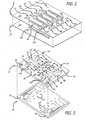
- Fig. 2 is a magnified exploded view illustrating filter layers 20, 24 of the stacked multilayer programmable filter of Fig. 1 .
- the intervening groundplane layer 22 of Fig. 1 is not shown in Fig. 2 .
- the five first-layer filter elements 96 and the five second-layer filter elements 104 are implemented as stripline filter elements with strategically patterned filter metalization 130 surrounded by clearance areas 132 in surrounding metal surfacing 134.
- Various input vertical RF transitions 52, 56, 36, 60, 64 and output vertical RF transitions 82, 86, 74, 90, 94 and accompanying mode-suppression holes 122 are more clearly visible in Fig. 2 .
- Fig. 3 is a more detailed view illustrating a Radio Frequency (RF) switching layer 14 and control-routing layer 16 of the stacked multilayer programmable filter 10 of Fig. 1 .
- the first ASIC controller 40 connects with the corresponding first set of routing paths 42 in the control-routing layer 16.
- the second ASIC controller 44 connects to the second set of routing paths 46 in the control-routing layer 16.
- the various connecting paths 42, 46 connect the ASIC controllers 40, 44 to various circuit-tuning stubs 140 in the input switching network 24 and the output switching network 26. Additional circuit paths connect the first ASIC controller 40 and the second ASIC controller 44 to the input switches 2-32 and the output switches 68, 70, 76, respectively.
- the control lines 42, 46 of Fig. 1 are not shown in Fig. 3 .
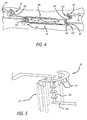
- Fig. 4 is a magnified view illustrating exemplary vertical waveguides 50, 52, 80, 82 of the programmable filter of Fig. 1 .
- the vertical RF transitions 50, 52, 80, 82 are implemented via center circular waveguide sections 142 surrounded by strategically positioned mode suppression holes 122.
- the exact numbers, sizes, and positions of the mode suppression holes 122 are application specific and may be readily determined by those skilled in the art with access to the present teachings to meet the needs of a given application.
- Well-known methods for transitioning stripline and microstrip circuits to/from circular waveguides, such as the exemplary vertical RF transitions 50, 52, 80, 82, may be employed to implement embodiments of the present invention without departing from the scope thereof.
- Fig. 5 is a further magnified view of an exemplary vertical RF transition of Fig. 4 .
- the mode-suppression holes 122 and accompanying surface metalization facilitate coupling the microstrip switching network circuitry (see switching network 24 of Fig. 1 ) to the vertical circular waveguide 50 and constituent center circular waveguide 142 while suppressing undesirable microwave signal propagation modes.
Landscapes
- Physics & Mathematics (AREA)
- Electromagnetism (AREA)
- Control Of Motors That Do Not Use Commutators (AREA)
- Waveguides (AREA)
- Waveguide Switches, Polarizers, And Phase Shifters (AREA)
- Production Of Multi-Layered Print Wiring Board (AREA)
Abstract
Description
- This invention relates to circuits. Specifically, the present invention relates to systems and methods for packaging and isolating circuits, such as microwave frequency converter circuits.
- Circuit isolation and packaging systems are employed in various demanding applications including microwave filter banks. Such applications demand compact packaging that minimizes electrical interference between components.
- Compact circuit isolation systems are particularly useful in microwave frequency converters and filter banks, where crosstalk between switches, filters, amplifiers, and signal converters is especially problematic. Conventionally, microwave frequency-shifter components are individually packaged in expensive double-sided cavitized housing assemblies, which are interconnected via wire, ribbon, and/or solder interconnects. Such component assemblies are often undesirably large and expensive. Furthermore, the various interconnects are prone to breakage, which reduces system reliability.
- Document
US 2003/0234706 shows a vertically-stacked filter employing a ground-aperture broadside-coupled resonator device. - Hence, a need exists in the art for a cost-effective and space-efficient system and method for assembling and packaging circuit components requiring electrical isolation.
- The need in the art is addressed by the compact multilayer signal processing system of the present invention. In the illustrative embodiment, the system is adapted for use with microwave signals. The system includes a first mechanism for receiving an input signal and selectively routing the input signal onto a first signal path. A second mechanism routes the input signal along the first signal path through one or more layers, including one or more groundplane layers, to a first circuit component for modifying the input signal and providing an adjusted signal in response thereto. A third mechanism outputs the adjusted signal.
- According to the invention, there is provided a multilayer signal processing system, comprising a first mechanism for receiving an input signal and selectively routing the input signal onto a first signal path; a second mechanism for routing the input signal along the first signal path vertically through one or more horizontal layers to a first circuit component that provides an adjusted signal in response to receipt of the input signal; and a third mechanism for outputting the adjusted signal, wherein the one or more horizontal layers include one or more ground plane layers, and wherein the first mechanism includes an input switching network in communication with one or more controllers for selectively switching the input signal onto one of plural input signal paths, the switching network disposed on a switching layer, wherein the second mechanism further includes a first input waveguide extending from the input switching network vertically through at least one groundplane layer and to an input end of the first circuit component, wherein the third mechanism includes a first output waveguide extending from an output end of the first circuit component and vertically through the at least one groundplane layer and to an output switching network disposed on the switching layer, and wherein the input switching network and the output switching network are microstrip switching networks, wherein the first circuit component is a stripline circuit component that is disposed on a circuit layer positioned between a first groundplane layer and a second groundplane layer, the first groundplane layer corresponding to the at least one groundplane layer. Further, the circuit layer includes plural circuit components, each coupled to a respective input waveguide and output waveguide that extend vertically through the first groundplane layer to the input switching network and the output switching network, respectively, wherein the system further includes one or more controllers coupled to the input switching network and/or to the output switching network and adapted to selectively activate or select a desired circuit component disposed on the circuit layer in response to a given operational mode of the multilayer signal processing system, wherein the system further includes one or more additional circuit layers disposed substantially adjacent to and parallel to the second groundplane layer on a side of the second groundplane layer opposite the circuit layer, and wherein the one or more additional circuit layers include one or more additional microwave filters disposed therein or thereon, and wherein the first input waveguide and the first output waveguide are equipped with parallel mode-suppression holes, the first input waveguide and the first output waveguide being circular waveguides.
- In a more specific embodiment, the first circuit component is a microwave filter. The circuit layer includes plural circuit components that are each coupled to a respective input waveguide and output waveguide that extend through the first groundplane layer to the input switching network and the output switching network, respectively.
- In the illustrative embodiment, the system further includes one or more controllers coupled to the input switching network and/or to the output switching network. The one or more controllers are adapted to selectively activate or select a desired circuit component disposed on the circuit layer in response to a given operational mode of the multilayer signal processing system. The system further includes one or more additional circuit layers disposed substantially adjacent to and parallel to the second groundplane layer on a side of the second groundplane layer opposite the circuit layer. The one or more additional circuit layers include one or more additional microwave filters disposed therein. The various waveguides, including the first input waveguide and the first output waveguide, are equipped with mode-suppression holes that parallel the waveguides, which are circular waveguides.
- One embodiment of the present invention is a stacked multilayer microwave filter with several filter elements. The unique positioning of the filter elements between or adjacent to groundplanes facilitates improved input/output isolation and significantly reduces the form factor required to implement the filter. Versatility and scalability of the filter is enhanced via use of unique input and output switching networks. The switching networks can switch a filter input signal to an appropriate layer and accompanying filter element and then selectively output the resulting filtered output signal while achieving minimal interference and maximum electrical isolation between filter input and output terminals. The vertical waveguides that couple the filter elements to the switching networks and that extend through one or more layers of the filter are equipped with special mode-suppression holes that further enhance filter response characteristics.
-
-
Fig. 1 is an exploded view of a stacked multilayer programmable microwave filter according to an embodiment of the present invention. -
Fig. 2 is a magnified view illustrating filter layers of the stacked multilayer programmable filter ofFig. 1 . -
Fig. 3 is a more detailed view illustrating a Radio Frequency (RF) switching layer and control signal routing layer of the stacked multilayer programmable filter ofFig. 1 . -
Fig. 4 is a magnified view illustrating exemplary vertical RF transitions of the programmable filter ofFig. 1 . -
Fig. 5 is a further magnified view of an exemplary vertical RF transition ofFig. 4 . - While the present invention is described herein with reference to illustrative embodiments for particular applications, it should be understood that the invention is not limited thereto. Those having ordinary skill in the art and access to the teachings provided herein will recognize additional modifications, applications, and embodiments within the scope thereof and additional fields in which the present invention would be of significant utility.
-
Fig. 1 is an exploded view of a stacked multilayerprogrammable microwave filter 10 according to an embodiment of the present invention. For clarity, various well-known components, such as power supplies, antennas, and so on, have been omitted from the figures. However, those skilled in the art with access to the present teachings will know which components to implement and how to implement them to meet the needs of a given application. - The stacked
programmable microwave filter 10 includes, from top to bottom, aswitching layer 14, a control-routing layer 16, afirst groundplane layer 18, afirst filter layer 20, asecond groundplane layer 22, and asecond filter layer 24. The various layers 14-24 are approximately parallel and coincident as shown inFig. 1 . The various layers 14-24 have a low-loss dielectric substrate core, which in the present embodiment is Duroid. Duroid may be ordered from Rogers Corp. - The
switching layer 14 includes aninput switching network 24 and anoutput switching network 26, which are positioned on opposite ends of atop surface 48 of theswitching layer 14. Theswitching networks first groundplane layer 18. - The
input switching network 24 includes aninput terminal 28 for receiving an input microwave signal. In the present specific embodiment, theinput terminal 28 connects to an input of a first 1-4switch 30. The first 1-4switch 30 selectively provides input to a second 1-4switch 32, a firstvertical RF transition 34, a secondvertical RF transition 36, and a third 1-4switch 38. - The second 1-4
switch 32 selectively provides input to a thirdvertical RF transition 50, a fourthvertical RF transition 52, a fifthvertical RF transition 54, and a sixthvertical RF transition 56. The third 1-4switch 38 selectively provides input to a seventhvertical RF transition 58, an eighthvertical RF transition 60, a ninthvertical RF transition 62, and a tenth verticalwaveguide RF transition 64. The 1-4switches controller 40. The control signals are routed through the control-routing layer 16 via a first set ofrouting paths 42, which are connected to the first ASIC controller and to theinput switching network 24 via vertical connections (not shown) extending through theswitching layer 14. - The
output switching network 26 includes a first 4-1switch 68, an output of which represents the output of the programmable stackedmicrowave filter 10 as provided at anoutput terminal 78. In response to receipt of control signals from asecond controller 44, the 4-1switch 68 selectively switches inputs from a second 4-1switch 70, a first outputvertical RF transition 72, a second outputvertical RF transition 74, and a third 4-1switch 76 to theoutput terminal 78. - The second 4-1
switch 70 selectively switches input from third, fourth, fifth, and sixth output vertical RF transitions 80-86, respectively, to an input of the first 4-1switch 68 in response to receipt of specific control signals from thesecond controller 44. Similarly, the third 4-1switch 76 selectively switches input from seventh, eighth, ninth, and tenth vertical RF transitions 88-94, respectively, to an input of the first 4-1switch 68. - The
various switches second ASIC controller 44. The control signals are routed through the control-routing layer 16 via a second set ofrouting paths 46, which are connected to the second ASIC controller and to theoutput switching network 26 via vertical connections (not shown) extending through theswitching layer 14. - The first, third, fifth, seventh, and ninth input
vertical RF transitions switching layer 14, the control-routing layer 16, and thefirst groundplane layer 18 to thefirst filter layer 20. At thefirst filter layer 20, the inputvertical RF transitions layer filter elements 96, three of which are visible inFig. 1 . The three visible first-layer filter elements include afirst filter element 98, asecond filter element 100, and athird filter element 102, which are coupled to the third inputvertical RF transition 50, the fifth inputvertical waveguide 54, and the first inputvertical waveguide 34, respectively. - The corresponding first, third, fifth, seventh, and ninth output vertical RF transitions 72, 80, 84, 88, 92, respectively, extend approximately perpendicularly through the
switching layer 14, the control-routing layer 16, and thefirst groundplane layer 18, and couple to outputs of the respective first-layer filter elements 96. Outputs of thefirst filter element 98,second filter element 100, andthird filter element 102 are coupled to the third outputvertical RF transition 80, fifth outputvertical RF transition 84, and the first outputvertical RF transition 74, respectively. - The second, fourth, sixth, eighth, and tenth input vertical RF transitions 36, 52, 56, 60, 64, respectively, extend approximately perpendicularly through the
switching layer 14, the control-routing layer 16, thefirst groundplane layer 18, thefirst filter layer 20, and thesecond groundplane layer 22. The input vertical RF transitions, 36, 52, 56, 60, 64 couple to inputs of five respective second-layer filter elements 104, three of which are visible inFig. 1 . The three visible second-layer filter elements include first, second, and third second-layer filter elements layer filter elements vertical RF transition 52, the sixth inputvertical waveguide 56, and the second inputvertical RF transition 36, respectively. - The second, fourth, sixth, eighth, and tenth output vertical RF transitions 74, 82, 86, 90, 94, respectively, extend approximately perpendicularly through the
switching layer 14, the control-routing layer 16, thefirst groundplane layer 18, thefirst filter layer 20, and thesecond groundplane layer 22. The output vertical RF transitions 74, 82, 86, 90, 94 couple to outputs of the five respective second-layer filter elements 104. Outputs of the visible secondlayer filter elements vertical RF transition 82, the sixth outputvertical RF transition 86, and the second outputvertical RF transition 74, respectively. - In the present specific embodiment, the control-
routing layer 16 is constructed substantially from dielectric material, such as Duroid. Atop surface 112 of the control-routing layer 16 is shown lacking surface metalization, but exhibiting plated through holes, i.e., coaxial structures corresponding to the various vertical RF transitions, such as the inputvertical waveguides - In the present embodiment, the
first groundplane layer 18 is implemented via a dielectric substrate exhibiting a first metal-platedtop surface 114 with vertical RF transition holes therein, which correspond to the various vertical RF transitions 34, 36, 50-64, 74, 76, 80-94. Similarly, thesecond groundplane layer 22 is implemented via a dielectric substrate exhibiting a second metal-platedtop surface 118 with vertical RF transition holes therein. Thesecond filter layer 24 also exhibits ametallic surface 120 disposed on a dielectric core. - In the
filter 10 ofFig. 1 , the variousvertical waveguides - The
first filter layer 20 exhibits a dielectric core with atop surface metalization 116 with strategically cleared areas corresponding to thefilter elements 96. Metalization within the strategically cleared areas is shaped to provide desired filtering operations on microwave signals passing through thefilter elements 96. Thesecond filter layer 24 is constructed similarly to thefirst filter layer 20 with the exception that themetallic surface 120 of thesecond filter layer 24 lacks waveguide holes therethrough. - The
filter elements 96, sandwiched between thefirst groundplane layer 114 and thesecond groundplane layer 118, are stripline filter elements. Consequently, thefilter elements 96 are homogenous and exhibit improved filter responses over certain other conventional filter elements. Thesecond filter layer 24 is constructed similarly to thefirst filter layer 20, with the exception that no waveguide holes through thesecond filter layer 24 are needed. - In operation, the
ASIC controllers input switching network 24 and theoutput switching network 26 to select a particular filter element from thefilter elements 96 of thefirst filter layer 20 or from thefilter elements 104 of thesecond filter layer 104. A particular filter element is selected when the appropriate switches of theinput network 24 and theoutput network 26 enable an input signal to pass through theinput switching network 14; through a corresponding input vertical RF transition; through the selected filter element; through the corresponding output vertical waveguide; and through theoutput switching network 26 to theoutput terminal 78. - In the present specific embodiment, the compact
stacked filter 10 configuration is adapted to filter electromagnetic energy within a microwave frequency band, such as between 4-15 GHz. Furthermore, in the present embodiment, only one filter element at a time is selected via thecontrollers - Strategic use of the
input switching network 24 and theoutput switching network 26 in combination with the use of groundplane layers 18, 22 between the input/output terminals terminals filter 10 significantly reduces filter space requirements, which is very important in various applications including missile, aircraft, and satellite systems. - Note that various layers, including the filter layers 20, 24 are coated with
metal 134. Themetalization 134 is connected to all ground planes 18, 22, which further improves signal isolation and cross talk. Note that the bottom filters 104-110 are stripline filters. Consequently, an additional groundplane layer (not shown) is included below thebottom filter layer 24. - The
ASIC controllers filter element ASIC controllers routing paths switches ASIC controllers - In the present embodiment, the
ASIC controllers appropriate filter elements input terminal 28. Thecontrollers controllers appropriate filter element controllers particular filter element controllers - In the present specific embodiments, the various vertical RF transitions 34, 36, 50-64, 74, 76, 80-94 exhibit mode-suppression holes, which are optimized to suppress undesirable signal modes travelling in the vertical RF transitions as discussed more fully below. The mode suppression holes 122 are implemented via metal-metal-plated through holes running substantially parallel to the vertical RF transitions 34, 36, 50-64, 74, 76, 80-94. In this embodiment, the vertical RF transitions 34, 36, 50-64, 74, 76, 80-94 are implemented via coaxial structures or circular waveguides. Waveguides other than circular waveguides may be employed without departing from the scope of the present invention.
- Those skilled in the art will appreciate that the stacked
filter 10 may be scaled to accommodate additional layers, additional filter elements per layer, or fewer layers with fewer filter elements per layer without departing from the scope of the present invention. Furthermore, thefilter elements - In the present specific embodiment, interfacing between the switching
networks - Those skilled in the art will appreciate that the stacked
programmable microwave filter 10 may be adapted for use with electromagnetic energy exhibiting frequencies other than microwave frequencies without departing from the scope of the present invention. Furthermore, thevarious microwave filters networks switches filter 10 exhibits twenty filter elements. - The unique use of the
switching networks groundplanes input terminal 28 and theoutput terminal 78. -
Fig. 2 is a magnified exploded view illustrating filter layers 20, 24 of the stacked multilayer programmable filter ofFig. 1 . For clarity, the interveninggroundplane layer 22 ofFig. 1 is not shown inFig. 2 . - In the present specific embodiment, the five first-
layer filter elements 96 and the five second-layer filter elements 104 are implemented as stripline filter elements with strategically patternedfilter metalization 130 surrounded byclearance areas 132 in surrounding metal surfacing 134. Various input vertical RF transitions 52, 56, 36, 60, 64 and output vertical RF transitions 82, 86, 74, 90, 94 and accompanying mode-suppression holes 122 are more clearly visible inFig. 2 . -
Fig. 3 is a more detailed view illustrating a Radio Frequency (RF) switchinglayer 14 and control-routing layer 16 of the stacked multilayerprogrammable filter 10 ofFig. 1 . Thefirst ASIC controller 40 connects with the corresponding first set ofrouting paths 42 in the control-routing layer 16. Similarly, thesecond ASIC controller 44 connects to the second set ofrouting paths 46 in the control-routing layer 16. - In the present specific embodiment, the various connecting
paths ASIC controllers stubs 140 in theinput switching network 24 and theoutput switching network 26. Additional circuit paths connect thefirst ASIC controller 40 and thesecond ASIC controller 44 to the input switches 2-32 and the output switches 68, 70, 76, respectively. For clarity, thecontrol lines Fig. 1 are not shown inFig. 3 . -
Fig. 4 is a magnified view illustrating exemplaryvertical waveguides Fig. 1 . The vertical RF transitions 50, 52, 80, 82 are implemented via centercircular waveguide sections 142 surrounded by strategically positioned mode suppression holes 122. The exact numbers, sizes, and positions of the mode suppression holes 122 are application specific and may be readily determined by those skilled in the art with access to the present teachings to meet the needs of a given application. Well-known methods for transitioning stripline and microstrip circuits to/from circular waveguides, such as the exemplary vertical RF transitions 50, 52, 80, 82, may be employed to implement embodiments of the present invention without departing from the scope thereof. -
Fig. 5 is a further magnified view of an exemplary vertical RF transition ofFig. 4 . The mode-suppression holes 122 and accompanying surface metalization facilitate coupling the microstrip switching network circuitry (see switchingnetwork 24 ofFig. 1 ) to the verticalcircular waveguide 50 and constituent centercircular waveguide 142 while suppressing undesirable microwave signal propagation modes. - Thus, the present invention has been described herein with reference to a particular embodiment for a particular application. Those having ordinary skill in the art and access to the present teachings will recognize additional modifications, applications, and embodiments within the scope thereof. It is therefore intended by the appended claims to cover any and all such applications, modifications and embodiments within the scope of the present invention.
Claims (2)
- A multilayer signal processing system (10), comprising
a first mechanism (24) for receiving an input signal and selectively routing the input signal onto a first signal path;
a second mechanism (50-56, 34, 36, 58-64) for routing the input signal along the first signal path vertically through one or more horizontal layers (16-22) to a first circuit component (96) that provides an adjusted signal in response to receipt of the input signal; and
a third mechanism (26, 80-86, 72, 74, 88-94) for outputting the adjusted signal,
wherein the one or more horizontal layers (16-22) include one or more ground plane layers (18, 22), and wherein the first mechanism (24) includes an input switching network (24) in communication with one or more controllers (40) for selectively switching the input signal onto one of plural input signal paths, the switching network (10) disposed on a switching layer (14),
wherein the second mechanism (50-56, 34, 36, 58-64) further includes a first input waveguide (50, 54, 34, 58, 62) extending from the input switching network (24) vertically through at least one groundplane layer (18) and to an input end of the first circuit component (96),
wherein the third mechanism (26, 80-86, 72, 74, 88-94) includes a first output waveguide (80, 84, 72, 88, 92) extending from an output end of the first circuit component (96) and vertically through the at least one groundplane layer (18) and to an output switching network (26) disposed on the switching layer (14), and wherein the input switching network (24) and the output switching network (26) are microstrip switching networks,
wherein the first circuit component (96) is a stripline circuit component that is disposed on a circuit layer (20) positioned between a first groundplane layer (18) and a second groundplane layer (22), the first groundplane layer (18) corresponding to the at least one groundplane layer (18),
characterized in that the circuit layer (20) includes plural circuit components (98, 100, 102), each coupled to a respective input waveguide (50, 54, 34) and output waveguide (80, 84, 72) that extend vertically through the first groundplane layer (18) to the input switching network (24) and the output switching network (26), respectively,
wherein the system (10) further includes one or more controllers (40, 78) coupled to the input switching network (24) and/or to the output switching network (26) and adapted to selectively activate or select a desired circuit component (96) disposed on the circuit layer (20) in response to a given operational mode of the multilayer signal processing system (10),
wherein the system (10) further includes one or more additional circuit layers (24) disposed substantially adjacent to and parallel to the second groundplane layer (22) on a side of the second groundplane layer (22) opposite the circuit layer (20), and wherein the one or more additional circuit layers (24) include one or more additional microwave filters (104) disposed therein or thereon, and
wherein the first input waveguide (50, 54, 34, 58, 62) and the first output waveguide (80, 84, 72, 88, 92) are equipped with parallel mode-suppression holes (122), the first input waveguide (50, 54, 34, 58, 62) and the first output waveguide (80, 84, 72, 88, 92) being circular waveguides. - The system (10) according to claim 1 wherein the first circuit component (96) is a microwave filter (96).
Applications Claiming Priority (2)
| Application Number | Priority Date | Filing Date | Title |
|---|---|---|---|
| US11/230,382 US7423498B2 (en) | 2005-09-20 | 2005-09-20 | Compact multilayer circuit |
| PCT/US2006/032611 WO2007035220A1 (en) | 2005-09-20 | 2006-08-22 | Compact multilayer circuit |
Publications (2)
| Publication Number | Publication Date |
|---|---|
| EP1927154A1 EP1927154A1 (en) | 2008-06-04 |
| EP1927154B1 true EP1927154B1 (en) | 2012-02-01 |
Family
ID=37497052
Family Applications (1)
| Application Number | Title | Priority Date | Filing Date |
|---|---|---|---|
| EP06789897A Not-in-force EP1927154B1 (en) | 2005-09-20 | 2006-08-22 | Compact multilayer circuit |
Country Status (10)
| Country | Link |
|---|---|
| US (1) | US7423498B2 (en) |
| EP (1) | EP1927154B1 (en) |
| JP (1) | JP4509208B2 (en) |
| KR (1) | KR101014472B1 (en) |
| AT (1) | ATE544193T1 (en) |
| AU (1) | AU2006292765B2 (en) |
| CA (1) | CA2606375C (en) |
| ES (1) | ES2381685T3 (en) |
| NO (1) | NO339769B1 (en) |
| WO (1) | WO2007035220A1 (en) |
Families Citing this family (4)
| Publication number | Priority date | Publication date | Assignee | Title |
|---|---|---|---|---|
| US8072297B2 (en) * | 2008-12-29 | 2011-12-06 | Qualcomm Incorporated | Apparatus and method for improving channel filter selectivity and performance using voltage variable impedance elements |
| US9178257B2 (en) | 2012-12-06 | 2015-11-03 | Anaren, Inc. | First and second microstrip networks stacked in an inverted arrangement to each other using an integrated support and shielding structure |
| FR2999813B1 (en) * | 2012-12-14 | 2017-07-14 | Cassidian Sas | HYPERFREQUENCY FILTRATION STRUCTURES |
| US10739521B2 (en) * | 2017-08-17 | 2020-08-11 | Xidas Inc. | Waveguide switch |
Family Cites Families (9)
| Publication number | Priority date | Publication date | Assignee | Title |
|---|---|---|---|---|
| JPH0758506A (en) * | 1993-08-09 | 1995-03-03 | Oki Electric Ind Co Ltd | Lc type dielectric filter and antenna multicoupler using it |
| US5471181A (en) * | 1994-03-08 | 1995-11-28 | Hughes Missile Systems Company | Interconnection between layers of striplines or microstrip through cavity backed slot |
| JP3031178B2 (en) * | 1994-09-28 | 2000-04-10 | 株式会社村田製作所 | Composite high frequency components |
| JP2001144511A (en) * | 1999-11-17 | 2001-05-25 | Mitsubishi Electric Corp | Converter for connecting planar waveguides |
| US6414570B1 (en) * | 2000-06-06 | 2002-07-02 | Raytheon Company | Low profile, high isolation and rejection x-band switched filter assembly |
| JP3866989B2 (en) * | 2001-02-27 | 2007-01-10 | 松下電器産業株式会社 | Antenna duplexer and mobile communication device using the same |
| US6798317B2 (en) * | 2002-06-25 | 2004-09-28 | Motorola, Inc. | Vertically-stacked filter employing a ground-aperture broadside-coupled resonator device |
| JP3810011B2 (en) * | 2003-08-08 | 2006-08-16 | Tdk株式会社 | High frequency switch module and multilayer substrate for high frequency switch module |
| US7084722B2 (en) * | 2004-07-22 | 2006-08-01 | Northrop Grumman Corp. | Switched filterbank and method of making the same |
-
2005
- 2005-09-20 US US11/230,382 patent/US7423498B2/en active Active
-
2006
- 2006-08-22 ES ES06789897T patent/ES2381685T3/en active Active
- 2006-08-22 KR KR1020087006718A patent/KR101014472B1/en active Active
- 2006-08-22 WO PCT/US2006/032611 patent/WO2007035220A1/en not_active Ceased
- 2006-08-22 JP JP2008531124A patent/JP4509208B2/en active Active
- 2006-08-22 AT AT06789897T patent/ATE544193T1/en active
- 2006-08-22 EP EP06789897A patent/EP1927154B1/en not_active Not-in-force
- 2006-08-22 CA CA2606375A patent/CA2606375C/en active Active
- 2006-08-22 AU AU2006292765A patent/AU2006292765B2/en not_active Ceased
-
2008
- 2008-04-21 NO NO20081894A patent/NO339769B1/en unknown
Also Published As
| Publication number | Publication date |
|---|---|
| AU2006292765A1 (en) | 2007-03-29 |
| JP2009509401A (en) | 2009-03-05 |
| KR20080036654A (en) | 2008-04-28 |
| EP1927154A1 (en) | 2008-06-04 |
| CA2606375C (en) | 2011-06-28 |
| JP4509208B2 (en) | 2010-07-21 |
| KR101014472B1 (en) | 2011-02-14 |
| NO20081894L (en) | 2008-04-21 |
| CA2606375A1 (en) | 2007-03-29 |
| ATE544193T1 (en) | 2012-02-15 |
| US7423498B2 (en) | 2008-09-09 |
| WO2007035220A1 (en) | 2007-03-29 |
| NO339769B1 (en) | 2017-01-30 |
| US20070063789A1 (en) | 2007-03-22 |
| AU2006292765B2 (en) | 2010-02-11 |
| ES2381685T3 (en) | 2012-05-30 |
Similar Documents
| Publication | Publication Date | Title |
|---|---|---|
| CN107579316B (en) | Based on microstrip line-line of rabbet joint broadband reverse phase function filter-divider | |
| US20120026052A1 (en) | Antennas with periodic shunt inductors | |
| CN111342174A (en) | Filtering phase shifter and antenna | |
| EP1855349A1 (en) | Band-pass filter element and high frequency module | |
| WO2020228402A1 (en) | Filtering, power-dividing and phase-shifting integrated antenna array feed network | |
| Nishikawa | RF front end circuit components miniaturized using dielectric resonators for cellular portable telephones | |
| US5426404A (en) | Electrical circuit using low volume multilayer transmission line devices | |
| JP2006352532A (en) | High frequency module | |
| EP1346432B1 (en) | Four port hybrid microstrip circuit of lange type | |
| US11165130B2 (en) | Three-way divider | |
| CA2606375C (en) | Compact multilayer circuit | |
| US6278341B1 (en) | Microstrip filter device | |
| US5789997A (en) | Bypassable wilkinson divider | |
| CN116759779B (en) | 5G millimeter wave filtering power division module | |
| US12155107B2 (en) | Filter, antenna module, and communication device | |
| US12506238B2 (en) | Filter and antenna module | |
| CN118472624A (en) | Millimeter wave filtering magneto-electric dipole antenna unit, antenna array and communication equipment | |
| EP1396934B1 (en) | Compact balun with rejection filter for 802.11a and 802.11b simultaneous operation | |
| JP5729636B2 (en) | Band pass filter and composite parts using the same | |
| JP5472672B2 (en) | High frequency circuit component and communication apparatus using the same | |
| CN119994425B (en) | Bandpass filter based on multilayer metal sheet waveguide | |
| US12614827B2 (en) | Wireless communication device comprising a phase shifting element having plural port units connected by plural conductive wires | |
| JP4794247B2 (en) | High frequency module | |
| Maloratsky | Design and technology tradeoffs in passive RF and microwave integrated circuits | |
| KR20260057854A (en) | High-power Antenna Filter and EMP Protection apparatus |
Legal Events
| Date | Code | Title | Description |
|---|---|---|---|
| PUAI | Public reference made under article 153(3) epc to a published international application that has entered the european phase |
Free format text: ORIGINAL CODE: 0009012 |
|
| 17P | Request for examination filed |
Effective date: 20080313 |
|
| AK | Designated contracting states |
Kind code of ref document: A1 Designated state(s): AT BE BG CH CY CZ DE DK EE ES FI FR GB GR HU IE IS IT LI LT LU LV MC NL PL PT RO SE SI SK TR |
|
| RIN1 | Information on inventor provided before grant (corrected) |
Inventor name: AKALE, TAMRAT Inventor name: CRNKOVICH, MICHAEL T. Inventor name: DRAPEAU, DAVID J. Inventor name: BARRIENTOS, EDUARDO, D., JR. Inventor name: MOYE, CHRISTOPHER A. Inventor name: DALCONZO, LAWRENCE |
|
| 17Q | First examination report despatched |
Effective date: 20091019 |
|
| GRAP | Despatch of communication of intention to grant a patent |
Free format text: ORIGINAL CODE: EPIDOSNIGR1 |
|
| DAX | Request for extension of the european patent (deleted) | ||
| GRAS | Grant fee paid |
Free format text: ORIGINAL CODE: EPIDOSNIGR3 |
|
| GRAA | (expected) grant |
Free format text: ORIGINAL CODE: 0009210 |
|
| AK | Designated contracting states |
Kind code of ref document: B1 Designated state(s): AT BE BG CH CY CZ DE DK EE ES FI FR GB GR HU IE IS IT LI LT LU LV MC NL PL PT RO SE SI SK TR |
|
| REG | Reference to a national code |
Ref country code: GB Ref legal event code: FG4D |
|
| REG | Reference to a national code |
Ref country code: CH Ref legal event code: EP Ref country code: AT Ref legal event code: REF Ref document number: 544193 Country of ref document: AT Kind code of ref document: T Effective date: 20120215 |
|
| REG | Reference to a national code |
Ref country code: DE Ref legal event code: R096 Ref document number: 602006027447 Country of ref document: DE Effective date: 20120329 |
|
| REG | Reference to a national code |
Ref country code: SE Ref legal event code: TRGR |
|
| REG | Reference to a national code |
Ref country code: ES Ref legal event code: FG2A Ref document number: 2381685 Country of ref document: ES Kind code of ref document: T3 Effective date: 20120530 Ref country code: NL Ref legal event code: VDEP Effective date: 20120201 |
|
| LTIE | Lt: invalidation of european patent or patent extension |
Effective date: 20120201 |
|
| PG25 | Lapsed in a contracting state [announced via postgrant information from national office to epo] |
Ref country code: NL Free format text: LAPSE BECAUSE OF FAILURE TO SUBMIT A TRANSLATION OF THE DESCRIPTION OR TO PAY THE FEE WITHIN THE PRESCRIBED TIME-LIMIT Effective date: 20120201 Ref country code: LT Free format text: LAPSE BECAUSE OF FAILURE TO SUBMIT A TRANSLATION OF THE DESCRIPTION OR TO PAY THE FEE WITHIN THE PRESCRIBED TIME-LIMIT Effective date: 20120201 Ref country code: IS Free format text: LAPSE BECAUSE OF FAILURE TO SUBMIT A TRANSLATION OF THE DESCRIPTION OR TO PAY THE FEE WITHIN THE PRESCRIBED TIME-LIMIT Effective date: 20120601 |
|
| PG25 | Lapsed in a contracting state [announced via postgrant information from national office to epo] |
Ref country code: LV Free format text: LAPSE BECAUSE OF FAILURE TO SUBMIT A TRANSLATION OF THE DESCRIPTION OR TO PAY THE FEE WITHIN THE PRESCRIBED TIME-LIMIT Effective date: 20120201 Ref country code: PL Free format text: LAPSE BECAUSE OF FAILURE TO SUBMIT A TRANSLATION OF THE DESCRIPTION OR TO PAY THE FEE WITHIN THE PRESCRIBED TIME-LIMIT Effective date: 20120201 Ref country code: PT Free format text: LAPSE BECAUSE OF FAILURE TO SUBMIT A TRANSLATION OF THE DESCRIPTION OR TO PAY THE FEE WITHIN THE PRESCRIBED TIME-LIMIT Effective date: 20120601 Ref country code: BE Free format text: LAPSE BECAUSE OF FAILURE TO SUBMIT A TRANSLATION OF THE DESCRIPTION OR TO PAY THE FEE WITHIN THE PRESCRIBED TIME-LIMIT Effective date: 20120201 Ref country code: GR Free format text: LAPSE BECAUSE OF FAILURE TO SUBMIT A TRANSLATION OF THE DESCRIPTION OR TO PAY THE FEE WITHIN THE PRESCRIBED TIME-LIMIT Effective date: 20120502 |
|
| REG | Reference to a national code |
Ref country code: AT Ref legal event code: MK05 Ref document number: 544193 Country of ref document: AT Kind code of ref document: T Effective date: 20120201 |
|
| PG25 | Lapsed in a contracting state [announced via postgrant information from national office to epo] |
Ref country code: CY Free format text: LAPSE BECAUSE OF FAILURE TO SUBMIT A TRANSLATION OF THE DESCRIPTION OR TO PAY THE FEE WITHIN THE PRESCRIBED TIME-LIMIT Effective date: 20120201 |
|
| PG25 | Lapsed in a contracting state [announced via postgrant information from national office to epo] |
Ref country code: DK Free format text: LAPSE BECAUSE OF FAILURE TO SUBMIT A TRANSLATION OF THE DESCRIPTION OR TO PAY THE FEE WITHIN THE PRESCRIBED TIME-LIMIT Effective date: 20120201 Ref country code: EE Free format text: LAPSE BECAUSE OF FAILURE TO SUBMIT A TRANSLATION OF THE DESCRIPTION OR TO PAY THE FEE WITHIN THE PRESCRIBED TIME-LIMIT Effective date: 20120201 Ref country code: CZ Free format text: LAPSE BECAUSE OF FAILURE TO SUBMIT A TRANSLATION OF THE DESCRIPTION OR TO PAY THE FEE WITHIN THE PRESCRIBED TIME-LIMIT Effective date: 20120201 Ref country code: RO Free format text: LAPSE BECAUSE OF FAILURE TO SUBMIT A TRANSLATION OF THE DESCRIPTION OR TO PAY THE FEE WITHIN THE PRESCRIBED TIME-LIMIT Effective date: 20120201 Ref country code: SI Free format text: LAPSE BECAUSE OF FAILURE TO SUBMIT A TRANSLATION OF THE DESCRIPTION OR TO PAY THE FEE WITHIN THE PRESCRIBED TIME-LIMIT Effective date: 20120201 |
|
| PG25 | Lapsed in a contracting state [announced via postgrant information from national office to epo] |
Ref country code: SK Free format text: LAPSE BECAUSE OF FAILURE TO SUBMIT A TRANSLATION OF THE DESCRIPTION OR TO PAY THE FEE WITHIN THE PRESCRIBED TIME-LIMIT Effective date: 20120201 |
|
| PLBE | No opposition filed within time limit |
Free format text: ORIGINAL CODE: 0009261 |
|
| STAA | Information on the status of an ep patent application or granted ep patent |
Free format text: STATUS: NO OPPOSITION FILED WITHIN TIME LIMIT |
|
| 26N | No opposition filed |
Effective date: 20121105 |
|
| PG25 | Lapsed in a contracting state [announced via postgrant information from national office to epo] |
Ref country code: AT Free format text: LAPSE BECAUSE OF FAILURE TO SUBMIT A TRANSLATION OF THE DESCRIPTION OR TO PAY THE FEE WITHIN THE PRESCRIBED TIME-LIMIT Effective date: 20120201 |
|
| REG | Reference to a national code |
Ref country code: DE Ref legal event code: R097 Ref document number: 602006027447 Country of ref document: DE Effective date: 20121105 |
|
| REG | Reference to a national code |
Ref country code: CH Ref legal event code: PL |
|
| PG25 | Lapsed in a contracting state [announced via postgrant information from national office to epo] |
Ref country code: MC Free format text: LAPSE BECAUSE OF NON-PAYMENT OF DUE FEES Effective date: 20120831 |
|
| PG25 | Lapsed in a contracting state [announced via postgrant information from national office to epo] |
Ref country code: CH Free format text: LAPSE BECAUSE OF NON-PAYMENT OF DUE FEES Effective date: 20120831 Ref country code: LI Free format text: LAPSE BECAUSE OF NON-PAYMENT OF DUE FEES Effective date: 20120831 |
|
| REG | Reference to a national code |
Ref country code: IE Ref legal event code: MM4A |
|
| PG25 | Lapsed in a contracting state [announced via postgrant information from national office to epo] |
Ref country code: IE Free format text: LAPSE BECAUSE OF NON-PAYMENT OF DUE FEES Effective date: 20120822 Ref country code: BG Free format text: LAPSE BECAUSE OF FAILURE TO SUBMIT A TRANSLATION OF THE DESCRIPTION OR TO PAY THE FEE WITHIN THE PRESCRIBED TIME-LIMIT Effective date: 20120501 |
|
| PG25 | Lapsed in a contracting state [announced via postgrant information from national office to epo] |
Ref country code: TR Free format text: LAPSE BECAUSE OF FAILURE TO SUBMIT A TRANSLATION OF THE DESCRIPTION OR TO PAY THE FEE WITHIN THE PRESCRIBED TIME-LIMIT Effective date: 20120201 |
|
| PG25 | Lapsed in a contracting state [announced via postgrant information from national office to epo] |
Ref country code: LU Free format text: LAPSE BECAUSE OF NON-PAYMENT OF DUE FEES Effective date: 20120822 |
|
| PG25 | Lapsed in a contracting state [announced via postgrant information from national office to epo] |
Ref country code: HU Free format text: LAPSE BECAUSE OF FAILURE TO SUBMIT A TRANSLATION OF THE DESCRIPTION OR TO PAY THE FEE WITHIN THE PRESCRIBED TIME-LIMIT Effective date: 20060822 |
|
| REG | Reference to a national code |
Ref country code: FR Ref legal event code: PLFP Year of fee payment: 11 |
|
| REG | Reference to a national code |
Ref country code: FR Ref legal event code: PLFP Year of fee payment: 12 |
|
| REG | Reference to a national code |
Ref country code: FR Ref legal event code: PLFP Year of fee payment: 13 |
|
| P01 | Opt-out of the competence of the unified patent court (upc) registered |
Effective date: 20230530 |
|
| PGFP | Annual fee paid to national office [announced via postgrant information from national office to epo] |
Ref country code: IT Payment date: 20230720 Year of fee payment: 18 Ref country code: GB Payment date: 20230720 Year of fee payment: 18 Ref country code: FI Payment date: 20230720 Year of fee payment: 18 Ref country code: ES Payment date: 20230901 Year of fee payment: 18 |
|
| PGFP | Annual fee paid to national office [announced via postgrant information from national office to epo] |
Ref country code: SE Payment date: 20230720 Year of fee payment: 18 Ref country code: FR Payment date: 20230720 Year of fee payment: 18 Ref country code: DE Payment date: 20230720 Year of fee payment: 18 |
|
| REG | Reference to a national code |
Ref country code: DE Ref legal event code: R119 Ref document number: 602006027447 Country of ref document: DE |
|
| REG | Reference to a national code |
Ref country code: SE Ref legal event code: EUG |
|
| PG25 | Lapsed in a contracting state [announced via postgrant information from national office to epo] |
Ref country code: FI Free format text: LAPSE BECAUSE OF NON-PAYMENT OF DUE FEES Effective date: 20240822 |
|
| GBPC | Gb: european patent ceased through non-payment of renewal fee |
Effective date: 20240822 |
|
| PG25 | Lapsed in a contracting state [announced via postgrant information from national office to epo] |
Ref country code: DE Free format text: LAPSE BECAUSE OF NON-PAYMENT OF DUE FEES Effective date: 20250301 |
|
| PG25 | Lapsed in a contracting state [announced via postgrant information from national office to epo] |
Ref country code: GB Free format text: LAPSE BECAUSE OF NON-PAYMENT OF DUE FEES Effective date: 20240822 |
|
| PG25 | Lapsed in a contracting state [announced via postgrant information from national office to epo] |
Ref country code: IT Free format text: LAPSE BECAUSE OF NON-PAYMENT OF DUE FEES Effective date: 20240822 |
|
| PG25 | Lapsed in a contracting state [announced via postgrant information from national office to epo] |
Ref country code: FR Free format text: LAPSE BECAUSE OF NON-PAYMENT OF DUE FEES Effective date: 20240831 |
|
| REG | Reference to a national code |
Ref country code: ES Ref legal event code: FD2A Effective date: 20250930 |
|
| PG25 | Lapsed in a contracting state [announced via postgrant information from national office to epo] |
Ref country code: ES Free format text: LAPSE BECAUSE OF NON-PAYMENT OF DUE FEES Effective date: 20240823 |
|
| PG25 | Lapsed in a contracting state [announced via postgrant information from national office to epo] |
Ref country code: SE Free format text: LAPSE BECAUSE OF NON-PAYMENT OF DUE FEES Effective date: 20240823 |