EP1926130A1 - Method of improving the surface of a semiconductor substrate - Google Patents
Method of improving the surface of a semiconductor substrate Download PDFInfo
- Publication number
- EP1926130A1 EP1926130A1 EP06291827A EP06291827A EP1926130A1 EP 1926130 A1 EP1926130 A1 EP 1926130A1 EP 06291827 A EP06291827 A EP 06291827A EP 06291827 A EP06291827 A EP 06291827A EP 1926130 A1 EP1926130 A1 EP 1926130A1
- Authority
- EP
- European Patent Office
- Prior art keywords
- silicon
- hole
- semiconductor substrate
- deposition step
- deposition
- Prior art date
- Legal status (The legal status is an assumption and is not a legal conclusion. Google has not performed a legal analysis and makes no representation as to the accuracy of the status listed.)
- Withdrawn
Links
Images


Classifications
-
- H—ELECTRICITY
- H10—SEMICONDUCTOR DEVICES; ELECTRIC SOLID-STATE DEVICES NOT OTHERWISE PROVIDED FOR
- H10P—GENERIC PROCESSES OR APPARATUS FOR THE MANUFACTURE OR TREATMENT OF DEVICES COVERED BY CLASS H10
- H10P50/00—Etching of wafers, substrates or parts of devices
-
- H—ELECTRICITY
- H10—SEMICONDUCTOR DEVICES; ELECTRIC SOLID-STATE DEVICES NOT OTHERWISE PROVIDED FOR
- H10P—GENERIC PROCESSES OR APPARATUS FOR THE MANUFACTURE OR TREATMENT OF DEVICES COVERED BY CLASS H10
- H10P14/00—Formation of materials, e.g. in the shape of layers or pillars
- H10P14/20—Formation of materials, e.g. in the shape of layers or pillars of semiconductor materials
- H10P14/27—Formation of materials, e.g. in the shape of layers or pillars of semiconductor materials using selective deposition, e.g. simultaneous growth of monocrystalline and non-monocrystalline semiconductor materials
-
- H—ELECTRICITY
- H10—SEMICONDUCTOR DEVICES; ELECTRIC SOLID-STATE DEVICES NOT OTHERWISE PROVIDED FOR
- H10P—GENERIC PROCESSES OR APPARATUS FOR THE MANUFACTURE OR TREATMENT OF DEVICES COVERED BY CLASS H10
- H10P52/00—Grinding, lapping or polishing of wafers, substrates or parts of devices
Definitions
- the invention relates to a method of improving a surface of a semiconductor substrate, said surface consisting at least partially of silicon.
- Defects of semiconductor substrates can be of very different origin and may occur in the bulk material of wafers or layers or on the surface of a structure.
- Deficient wafers like wafers or layers with holes or scratches on their surface or with oxide precipitates or so-called "HF-defects", which are present in or on a wafer and will be apparent by an HF-etch step, are mostly not suitable for further use.
- a wafer treatment of a wafer surface such as an etching step or a CMP step can be used to remove or to reduce the number or the size of defects at or near the wafer surface.
- Typical etchants are halogen bearing compounds such as HCl, HBr, HI, HF, and others.
- the etchant can also be a fluorine bearing compound such as SF 6 , or C x F x .
- the thermal treatment can be performed in a furnace or in a tool for rapid thermal processing (RTP).
- a defective wafer such as a cleaved film can be subjected to a combination of etching and deposition at very high temperature using a combination of etchant and deposition gases to result in a better surface quality.
- the method comprises a deposition step comprising a selective epitaxial deposition of silicon on silicon in at least one hole on the surface of said semiconductor substrate.
- the invention makes it possible to deposit silicon in said hole to seal or to close said hole selectively with high-quality mono-crystalline silicon material wherein a formation of polycrystalline silicon is avoided leading to the effect that the original hole disappears from the surface and the resulting repaired surface gets a high surface quality which is comparable to surfaces which are free from holes or defects from the outset.
- said deposition step comprises a selective growth of silicon on at least a part of a side wall of said hole.
- a hole in a silicon layer lying on another material can be closed by a gradual growth beginning from the side walls of the corresponding hole.
- said method comprises an etching step applied on the surface of the semiconductor substrate before the deposition step, said etching step comprising an etch-back of at least one defect being on the surface of the semiconductor substrate whereby forming said at least one hole on the surface.
- said deposition step is applied at least until the at least one hole is plugged with silicon.
- it can be sensible or sufficient only to plug the hole so that the hole is closed wherein it is of minor interest whether the whole hole is filled with silicon or not.
- the former hole in the surface of the semiconductor structure treated with this method is closed so that this semiconductor structure can be used for further processing.
- said deposition step is applied at least until the at least one hole is filled with silicon.
- the former hole can be fully removed and the resulting structure can be provided with a high-quality both at and under the surface.
- said etching step comprises a HF-dip to etch-back oxide containing defects at the surface of said semiconductor structure.
- An HF-etch step removes effectively oxide and thus reveals oxide containing defects at the surface resulting in a formation of holes on said surface which in turn can be closed with the selective deposition of silicon on silicon.
- etchant and silicon containing gas are used as source gas.
- HCl as the etchant and SiH 2 Cl 2 as the silicon containing gas are especially well suited material for a high-quality selective deposition of monocrystalline silicon since the respective source gas highly prevents nucleation of silicon on oxide surfaces or walls which would result in a growth of polysilicon.
- favorable etchant concentrations are a few % of the total volume of the source gas.
- silicon is deposited in the deposition step up to a thickness corresponding at least to about one half of the diameter of the hole on the surface. This thickness has been shown to be especially advantageous for a solid and durable sealing of the respective hole.
- H 2 bake at about 650°C, preferably for about 2 minutes, on the semiconductor structure before the deposition step. This relatively low-temperature H 2 bake leads to an effective removal of contaminants but to a low risk of agglomeration of silicon during the deposition step.
- said deposition step is performed under reduced pressure, for example from about 20 Torr to 80 Torr.
- reduced pressure for example from about 20 Torr to 80 Torr.
- the thickness of silicon on the surface of the semiconductor substrate is reduced before and/or after said deposition step. This enables a reduction of the final thickness of the treated semiconductor substrate, which can be in particular of importance in repairing of SOl wafers.
- Fig. 1 schematically shows a SOI substrate 1 containing at least one defect such as a HF-defect or the shown oxide precipitate 2.
- the SOI substrate 1 is only shown exemplarily to demonstrate the principle of the present invention, wherein the present invention can also be used to improve the surface quality of another semiconductor substrate like a silicon wafer or any other substrate having on top at least partially silicon.
- it is not necessary to provide a substrate with an oxide layer, as shown in Fig. 1 to apply the inventive idea of repairing this substrate.
- the inventive method is also applicable to other materials such as silicon alloys, for example SiGe structures.
- the SOl substrate of Fig. 1 comprises a silicon substrate 3, on which a buried oxide 4 is formed, and has on top a silicon layer 5 having a certain thickness t 1 and comprising the at least one defect such as the shown oxide precipitate 2 situated at a surface 6 of the silicon layer 5 and extending into the bulk region of this silicon layer 5.
- the only one defect shown in Fig. 1 consists in the example shown mainly of silicon dioxide and is only shown exemplarily to illustrate the idea of the invention, wherein in fact considerably more defects as the one defect shown can be present in or on the silicon layer 5.
- the oxide precipitate of Fig. 1 shall show exemplarily a "small" defect having a rather small lateral extension being in the order of magnitude of the thickness of the silicon layer 5 or smaller.
- the structure shown in Fig. 1 is subjected to HF leading to an at least partial removal of the oxide precipitate 2 beginning at the surface 6 and continuing in the depth of the oxide precipitate 2 without or with only minimum effects on the silicon layer 5 since HF etches silicon with a much lower rate than silicon dioxide.
- the HF dip treatment can be used to etch-back HF-defects to create space which can be filled or plugged in a subsequent process step described below with defect-free silicon.
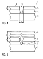
- a longer HF dip can result in a hole 17 extending into the buried oxide layer 4 underlying the silicon layer 5.
- Fig. 3 schematically shows the SOI substrate of Fig. 2 after a selective deposition of silicon using Selective Epitaxial Growth (SEG) wherein the dashed lines and the direction of arrow A shall demonstrate schematically the progress of silicon deposition leading to a thickness t 2 of the resulting silicon top layer 8.
- SEG Selective Epitaxial Growth
- SEG is an epitaxial deposition process which has the advantage that it will prevent, in general, nucleation of silicon on a polycrystalline or an amorphous material like an oxide surface.
- An epitaxial silicon growth does only occur on mono-crystalline silicon.
- wet cleaning and in situ H 2 bake at about 650°C to 800°C for about 2 minutes under a reduced pressure, for example of 20 Torr is applied on the SOl-structure shown in Fig. 2 in order to remove C, O and F contaminants on the surface 6. If a bulk material such as a silicon wafer shall be repaired instead of the SOl-structure shown in Fig. 2 , the H 2 bake is performed at higher temperatures. If the silicon layer 5 is thinner than 20 nm, temperatures in excess of about 700°C should not be applied during H 2 bake on the SOl structure 1 to prevent a Si film retraction during SEG.
- the H 2 bake can be performed at temperatures up to 850°C or higher. Although in comparison with other conventional H 2 bake processes the recommended temperature of the invention for the H 2 bake is relatively low, the contaminants left on the surface 6 prior SEG silicon formation have not such an impact on the electrical properties of the resulting devices since they will be partially consumed or removed during later procedural steps.
- the H 2 bake is followed by a ramping-up of the temperature up to the temperature of the SEG step.
- the SEG of silicon is performed in a reduced atmosphere of about 20 Torr applying a relatively low temperature of about 650°C to 800°C and using for instance HCl as an etchant and for instance SiH 2 Cl 2 as the Si gaseous precursor and using H 2 as carrier gas, optionally with some gaseous hydrochloric acid to achieve full selectivity vs. SiO 2 and Si 3 N 4 .
- the SEG step should be performed at about 750°C using for example a SiH 2 Cl 2 + HCl chemistry to avoid any severe islands formation during silicon growth.
- the growth rate of silicon should be fairly low which can be achieved by source gas reduction wherein the reaction rate is reduced in the presence of HCl.
- silicon grows during SEG on the surface 6 of the silicon layer 5, on the open silicon at the side walls of the etched hole 7 as well as on the already grown silicon in such a way that the hole in the silicon layer 6 is gradually closed or plugged with silicon.
- a thickness t 2 of silicon with a high surface quality is reached on top of the silicon layer 6.
- the non-etched part of the defect 2 and a small unfilled residual part of the etched hole 7 are buried in the structure above the oxide surface where no nucleation occurs.
- the defect shown in Fig. 1 is fully etched away during the etching step and the etching step is performed in such a way that the buried oxide below the silicon layer 5 is not influenced, the defect(s) in or on the silicon layer 5 can be fully removed and replaced by high-quality silicon resulting in a nearly perfect structure having a surface 6 without defects or with only a minimum of defects.
- the opening of the hole 7 is sealed if the thickness t 2 of the deposited silicon layer is about 1 ⁇ 2 of the diameter w of the hole 7. Therefore, a minimum epitaxial thickness t 2 of about 1 ⁇ 2 of the hole 7 diameter w is necessary in order to seal the opening.
- the structure of Fig. 1 is etched deeper than in Fig. 2 during the etching step so that the buried oxide 4 lying under the silicon layer 5 was affected.
- the resulting hole 17 in the SOI structure 1 has silicon side walls formed by the silicon layer 5 and a bottom of silicon dioxide formed by the attacked buried oxide layer 4.
- the hole 17 of the SOl substrate of Fig. 4 is gradually filled during the SEG process with silicon.
- the hole 17 is plugged and covered with high-quality mono-crystalline silicon wherein a little cavity 27 can remain in the buried oxide layer 4 which hole 27 is not filled with silicon.
- Figs. 6 and 7 show schematically that the idea of the invention can also be used to improve the surface quality of substrate or structures having on top layer with "larger" holes such as "wells” having a large aspect ratio wherein the width w of the holes is a few times higher than their depth h (w / h >> 1).
- the diameter w of the holes 37 and 47 is about 0.5 ⁇ m
- the silicon top layer 5 has a thickness of about 50 nm
- the oxide layer 4 has a thickness of about 150 nm resulting in an aspect ratio of 2.5.
- the arched lines in the Figs. 6 and 7 indicate the sequence of epitaxial deposition.
- a SOI substrate 10 is shown, said SOI substrate 10 consisting of a silicon substrate 3, an oxide layer 4 on the silicon substrate 3 and a thin silicon top layer 5.
- the SOl substrate 10 has a hole 37 through the silicon top layer 5 and the oxide layer 4.
- the hole 37 has in the example shown nearly perpendicular, flat side walls formed, for instance, by photolithography and etching, but can have, in other not shown embodiments of the present invention, also inclined and/or rough side walls.
- the bottom 39 of the hole 37 is formed by the surface of the silicon substrate 3 and consists, therefore, of mono-crystalline silicon.
- the surface 6 of the structure 10 can be smoothed and straightened by filling the hole 37 in accordance with the present invention using the Selective Epitaxial Growth of silicon.
- a HF dip prior SEG is not necessary but can, for instance if native oxide should be removed from the bottom 39, be applied.
- a SEG step in accordance with the exemplification of Figs. 3 and 5 .
- silicon grows on the exposed silicon areas of the structure 10, in particular on the surface 6 of the silicon layer 5, on the exposed side walls 20, 21 of the silicon layer 5 and on the bottom 39 of the hole 37 as well as on the already grown silicon.
- the silicon grows in such a way that the hole 37 is gradually filled during SEG with mono-crystalline silicon wherein it can be possible that at the end of SEG very small buried cavities in the former "large" hole 37 remain which are not overgrown.
- Fig. 7 schematically shows an oxide hole or well 47 in a SOl substrate 11 sealed with silicon in accordance with the present invention.
- the SOl substrate 11 consists, like the SOl substrate 10 of Fig. 6 , of a silicon substrate 3, an oxide layer 4 and a silicon top layer 5 having a surface 6 with the "large" hole 47 having a more lateral than vertical extension.
- the SOI substrate 11 has on the bottom 49 of the hole 47 a residual thickness of SiO 2 of the not completely etched oxide layer 4 so that the bottom 49 consists of silicon dioxide.
- the silicon growing during SEG does not form on the bottom 49 but only on the surface 6 and the exposed side walls 20, 21 of the silicon layer 5 as well as on the already grown silicon resulting in an overgrowth of the hole 47 from the sides what can be proceeded till the hole 47 is closed.
- the thickness of the structures as shown in the Figs. 3 , 5 , 6 or 7 can be adjusted onto certain requirements by a reduction of the thickness of the grown silicon using oxidation, CMP and/or silicon etching.
- the final SOI thickness can also be thinned by an initial reduction of the thickness t 1 of the silicon top layer 5, for instance by oxidation, CMP and/or silicon etching prior to HF-dip or SEG, or by a combination of initial and final thickness reduction.
- additional finishing steps, like smoothing annealing can be performed on the final structure.
- the present invention offers a method for repairing defects or closing holes in a surface of a semiconductor substrate consisting at least partially of silicon.
- the method of the invention can be used to repair defects in silicon substrates as well as in Semiconductor on Insulator Substrates (SeOI) like Silicon on Insulator (SOI) wafers.
- SiOI Semiconductor on Insulator Substrates
- SOI Silicon on Insulator
- the quality of a defective semiconductor substrate can be enhanced making this substrate attractive for further fabrication processes.
- SOI substrates repaired with the method of the invention are especially well suited for prospective applications where thicker SOl substrates are required.
- the final thickness (t 1 + t 2 ) of a repaired substrate can be adapted in such a way that the repaired wafer can rejoin the original product group.
- SOI wafers repaired with the method of the invention are applicable for the formation of advanced substrates using Direct Substrates Bonding (DSB). Furthermore, the method according the present invention allows repair of defects occurring in structures produced by the so-called "Smart Cut ® "-process.
- inventive technology is in particular advantageous for repairing deep defects or for closing large holes in a semiconductor substrate which can not be repaired or closed using the known surface smoothing methods.
Abstract
Description
- The invention relates to a method of improving a surface of a semiconductor substrate, said surface consisting at least partially of silicon.
- In semiconductor device production, it is more and more important to provide semiconductor substrates with a very high quality. Defects of semiconductor substrates can be of very different origin and may occur in the bulk material of wafers or layers or on the surface of a structure. Deficient wafers, like wafers or layers with holes or scratches on their surface or with oxide precipitates or so-called "HF-defects", which are present in or on a wafer and will be apparent by an HF-etch step, are mostly not suitable for further use.
- To improve the surface characteristic of a defective wafer, a wafer treatment of a wafer surface such as an etching step or a CMP step can be used to remove or to reduce the number or the size of defects at or near the wafer surface. Typical etchants are halogen bearing compounds such as HCl, HBr, HI, HF, and others. The etchant can also be a fluorine bearing compound such as SF6, or CxFx. Moreover or in addition, it is possible to treat a defect containing wafer thermally, preferably in a hydrogen bearing environment, to smooth it and to diminish its defects. The thermal treatment can be performed in a furnace or in a tool for rapid thermal processing (RTP). According to another approach disclosed in the document
US 6,287,941 B1 , a defective wafer such as a cleaved film can be subjected to a combination of etching and deposition at very high temperature using a combination of etchant and deposition gases to result in a better surface quality. - Although such methods lead, in the first instance, to a superficial improvement of the surface condition of a defective wafer by smoothing, abrasion or defect covering of the respective wafer, the known methods are mostly very laborious and the corresponding defects cannot really be repaired.
- It is therefore the object of the present invention to provide a method of improving a surface of a semiconductor substrate, said surface consisting at least partially of silicon, wherein with this method defects present in or on the semiconductor substrate can be really repaired to provide a semiconductor substrate with a high surface quality.
- This object is solved by a method of the above mentioned type wherein the method comprises a deposition step comprising a selective epitaxial deposition of silicon on silicon in at least one hole on the surface of said semiconductor substrate.
- The invention makes it possible to deposit silicon in said hole to seal or to close said hole selectively with high-quality mono-crystalline silicon material wherein a formation of polycrystalline silicon is avoided leading to the effect that the original hole disappears from the surface and the resulting repaired surface gets a high surface quality which is comparable to surfaces which are free from holes or defects from the outset.
- In a preferred variant of the invention, said deposition step comprises a selective growth of silicon on at least a part of a side wall of said hole. In this manner, a hole in a silicon layer lying on another material can be closed by a gradual growth beginning from the side walls of the corresponding hole. This kind of method is, in particular, of interest for closing large holes in SOI structures with high-quality silicon.
- In another favorable variant of the invention, said method comprises an etching step applied on the surface of the semiconductor substrate before the deposition step, said etching step comprising an etch-back of at least one defect being on the surface of the semiconductor substrate whereby forming said at least one hole on the surface. By means of this etching step, the at least one defect can be removed leading to at least one hole at the surface of the semiconductor structure which can be closed with silicon with the result that the original defect can be removed and a nearly perfect repaired surface of the originally defective semiconductor structure can be provided.
- According to an advantageous embodiment of the invention, said deposition step is applied at least until the at least one hole is plugged with silicon. In some cases, it can be sensible or sufficient only to plug the hole so that the hole is closed wherein it is of minor interest whether the whole hole is filled with silicon or not. In any case, as a result, the former hole in the surface of the semiconductor structure treated with this method is closed so that this semiconductor structure can be used for further processing.
- Preferably, said deposition step is applied at least until the at least one hole is filled with silicon. In doing so, the former hole can be fully removed and the resulting structure can be provided with a high-quality both at and under the surface.
- Advantageously, said etching step comprises a HF-dip to etch-back oxide containing defects at the surface of said semiconductor structure. An HF-etch step removes effectively oxide and thus reveals oxide containing defects at the surface resulting in a formation of holes on said surface which in turn can be closed with the selective deposition of silicon on silicon.
- According to a preferred embodiment of the invention, in said selective epitaxial deposition, etchant and silicon containing gas are used as source gas. HCl as the etchant and SiH2Cl2 as the silicon containing gas are especially well suited material for a high-quality selective deposition of monocrystalline silicon since the respective source gas highly prevents nucleation of silicon on oxide surfaces or walls which would result in a growth of polysilicon. For selective epitaxial growth, favorable etchant concentrations are a few % of the total volume of the source gas.
- In a preferred example of the present invention, silicon is deposited in the deposition step up to a thickness corresponding at least to about one half of the diameter of the hole on the surface. This thickness has been shown to be especially advantageous for a solid and durable sealing of the respective hole.
- In order to remove contaminants from the etched surface, it has been shown as advantageous to apply a H2 bake at about 650°C, preferably for about 2 minutes, on the semiconductor structure before the deposition step. This relatively low-temperature H2 bake leads to an effective removal of contaminants but to a low risk of agglomeration of silicon during the deposition step.
- It has been shown to be advantageous to perform said deposition step at about 750°C. This deposition temperature is lower than the temperature used in standard epitaxy processes. That way, agglomeration of silicon can be avoided, in particular if SOI structures with thin silicon top layers are treated with the inventive method.
- In a further embodiment of the invention, said deposition step is performed under reduced pressure, for example from about 20 Torr to 80 Torr. The deposition in a reduced atmosphere with this pressure leads to especially good and homogenous silicon formation.
- In another variant of the invention, the thickness of silicon on the surface of the semiconductor substrate is reduced before and/or after said deposition step. This enables a reduction of the final thickness of the treated semiconductor substrate, which can be in particular of importance in repairing of SOl wafers.
- Advantageous embodiments of the invention will be described in the following with respect to the figures in which
-
Fig. 1 schematically shows a SOI substrate containing a defect; -
Fig. 2 schematically shows the substrate ofFig. 1 after a short HF dip; -
Fig. 3 schematically shows the substrate ofFig. 2 after selective deposition of silicon; -
Fig. 4 schematically shows after a deeper HF dip; -
Fig. 5 schematically shows the substrate ofFig. 4 after selective deposition of silicon; -
Fig. 6 schematically shows a hole in a SOI-substrate sealed with silicon in accordance with the present invention; and -
Fig. 7 schematically shows another hole in a SOl-substrate sealed with silicon in accordance with the present invention. -
Fig. 1 schematically shows a SOI substrate 1 containing at least one defect such as a HF-defect or the shown oxide precipitate 2. The SOI substrate 1 is only shown exemplarily to demonstrate the principle of the present invention, wherein the present invention can also be used to improve the surface quality of another semiconductor substrate like a silicon wafer or any other substrate having on top at least partially silicon. In particular, it is not necessary to provide a substrate with an oxide layer, as shown inFig. 1 , to apply the inventive idea of repairing this substrate. - The inventive method is also applicable to other materials such as silicon alloys, for example SiGe structures.
- The SOl substrate of
Fig. 1 comprises asilicon substrate 3, on which a buriedoxide 4 is formed, and has on top asilicon layer 5 having a certain thickness t1 and comprising the at least one defect such as the shown oxide precipitate 2 situated at asurface 6 of thesilicon layer 5 and extending into the bulk region of thissilicon layer 5. The only one defect shown inFig. 1 consists in the example shown mainly of silicon dioxide and is only shown exemplarily to illustrate the idea of the invention, wherein in fact considerably more defects as the one defect shown can be present in or on thesilicon layer 5. The oxide precipitate ofFig. 1 shall show exemplarily a "small" defect having a rather small lateral extension being in the order of magnitude of the thickness of thesilicon layer 5 or smaller. - According to
Fig. 2 , the structure shown inFig. 1 is subjected to HF leading to an at least partial removal of theoxide precipitate 2 beginning at thesurface 6 and continuing in the depth of theoxide precipitate 2 without or with only minimum effects on thesilicon layer 5 since HF etches silicon with a much lower rate than silicon dioxide. In the same way, the HF dip treatment can be used to etch-back HF-defects to create space which can be filled or plugged in a subsequent process step described below with defect-free silicon. - The longer the HF dip the deeper is the resulting
hole 7 in thesurface 6 of the SOl structure 1. As shown inFig. 4 , a longer HF dip can result in ahole 17 extending into the buriedoxide layer 4 underlying thesilicon layer 5. -
Fig. 3 schematically shows the SOI substrate ofFig. 2 after a selective deposition of silicon using Selective Epitaxial Growth (SEG) wherein the dashed lines and the direction of arrow A shall demonstrate schematically the progress of silicon deposition leading to a thickness t2 of the resultingsilicon top layer 8. - SEG is an epitaxial deposition process which has the advantage that it will prevent, in general, nucleation of silicon on a polycrystalline or an amorphous material like an oxide surface. An epitaxial silicon growth does only occur on mono-crystalline silicon.
- Prior to the SEG step, wet cleaning and in situ H2 bake at about 650°C to 800°C for about 2 minutes under a reduced pressure, for example of 20 Torr is applied on the SOl-structure shown in
Fig. 2 in order to remove C, O and F contaminants on thesurface 6. If a bulk material such as a silicon wafer shall be repaired instead of the SOl-structure shown inFig. 2 , the H2 bake is performed at higher temperatures. If thesilicon layer 5 is thinner than 20 nm, temperatures in excess of about 700°C should not be applied during H2 bake on the SOl structure 1 to prevent a Si film retraction during SEG. Only in cases in which the film thickness of thesilicon layer 5 is higher than 20 nm, the H2 bake can be performed at temperatures up to 850°C or higher. Although in comparison with other conventional H2 bake processes the recommended temperature of the invention for the H2 bake is relatively low, the contaminants left on thesurface 6 prior SEG silicon formation have not such an impact on the electrical properties of the resulting devices since they will be partially consumed or removed during later procedural steps. The H2 bake is followed by a ramping-up of the temperature up to the temperature of the SEG step. - To avoid an agglomeration of silicon, the SEG of silicon is performed in a reduced atmosphere of about 20 Torr applying a relatively low temperature of about 650°C to 800°C and using for instance HCl as an etchant and for instance SiH2Cl2 as the Si gaseous precursor and using H2 as carrier gas, optionally with some gaseous hydrochloric acid to achieve full selectivity vs. SiO2 and Si3N4. For an
ultra-thin silicon layer 6 with a thickness t1 in the range of 3 to 10 nm, the SEG step should be performed at about 750°C using for example a SiH2Cl2 + HCl chemistry to avoid any severe islands formation during silicon growth. During SEG, the growth rate of silicon should be fairly low which can be achieved by source gas reduction wherein the reaction rate is reduced in the presence of HCl. - As shown schematically in
Fig. 3 by the dashed lines, silicon grows during SEG on thesurface 6 of thesilicon layer 5, on the open silicon at the side walls of the etchedhole 7 as well as on the already grown silicon in such a way that the hole in thesilicon layer 6 is gradually closed or plugged with silicon. After a certain process time, a thickness t2 of silicon with a high surface quality is reached on top of thesilicon layer 6. The non-etched part of thedefect 2 and a small unfilled residual part of the etchedhole 7 are buried in the structure above the oxide surface where no nucleation occurs. - If the defect shown in
Fig. 1 is fully etched away during the etching step and the etching step is performed in such a way that the buried oxide below thesilicon layer 5 is not influenced, the defect(s) in or on thesilicon layer 5 can be fully removed and replaced by high-quality silicon resulting in a nearly perfect structure having asurface 6 without defects or with only a minimum of defects. - During the SEG deposition step, it can be assumed that the opening of the
hole 7 is sealed if the thickness t2 of the deposited silicon layer is about ½ of the diameter w of thehole 7. Therefore, a minimum epitaxial thickness t2 of about ½ of thehole 7 diameter w is necessary in order to seal the opening. - With reference to
Fig. 4 , the structure ofFig. 1 is etched deeper than inFig. 2 during the etching step so that the buriedoxide 4 lying under thesilicon layer 5 was affected. The resultinghole 17 in the SOI structure 1 has silicon side walls formed by thesilicon layer 5 and a bottom of silicon dioxide formed by the attacked buriedoxide layer 4. - As shown schematically in
Fig. 5 , thehole 17 of the SOl substrate ofFig. 4 is gradually filled during the SEG process with silicon. At a certain time of growth, thehole 17 is plugged and covered with high-quality mono-crystalline silicon wherein alittle cavity 27 can remain in the buriedoxide layer 4 whichhole 27 is not filled with silicon. - The
Figs. 6 and 7 show schematically that the idea of the invention can also be used to improve the surface quality of substrate or structures having on top layer with "larger" holes such as "wells" having a large aspect ratio wherein the width w of the holes is a few times higher than their depth h (w / h >> 1). In the examples shown inFigs. 6 and 7 , the diameter w of theholes silicon top layer 5 has a thickness of about 50 nm and theoxide layer 4 has a thickness of about 150 nm resulting in an aspect ratio of 2.5. - The arched lines in the
Figs. 6 and 7 indicate the sequence of epitaxial deposition. - With reference to
Fig. 6 , aSOI substrate 10 is shown, saidSOI substrate 10 consisting of asilicon substrate 3, anoxide layer 4 on thesilicon substrate 3 and a thinsilicon top layer 5. TheSOl substrate 10 has ahole 37 through thesilicon top layer 5 and theoxide layer 4. Thehole 37 has in the example shown nearly perpendicular, flat side walls formed, for instance, by photolithography and etching, but can have, in other not shown embodiments of the present invention, also inclined and/or rough side walls. The bottom 39 of thehole 37 is formed by the surface of thesilicon substrate 3 and consists, therefore, of mono-crystalline silicon. - In the embodiment shown in
Fig. 6 , thesurface 6 of thestructure 10 can be smoothed and straightened by filling thehole 37 in accordance with the present invention using the Selective Epitaxial Growth of silicon. In the particular case shown inFig. 6 , a HF dip prior SEG is not necessary but can, for instance if native oxide should be removed from the bottom 39, be applied. As explained above with reference toFigs. 3 and5 , it is furthermore possible to apply a wet cleaning step before SEG. - As also explained above with reference to
Figs. 3 and5 , prior to SEG a H2 bake is applied. - Then follows a SEG step in accordance with the exemplification of
Figs. 3 and5 . During the SEG step, silicon grows on the exposed silicon areas of thestructure 10, in particular on thesurface 6 of thesilicon layer 5, on the exposedside walls silicon layer 5 and on the bottom 39 of thehole 37 as well as on the already grown silicon. As result, the silicon grows in such a way that thehole 37 is gradually filled during SEG with mono-crystalline silicon wherein it can be possible that at the end of SEG very small buried cavities in the former "large"hole 37 remain which are not overgrown. -
Fig. 7 schematically shows an oxide hole or well 47 in aSOl substrate 11 sealed with silicon in accordance with the present invention. TheSOl substrate 11 consists, like theSOl substrate 10 ofFig. 6 , of asilicon substrate 3, anoxide layer 4 and asilicon top layer 5 having asurface 6 with the "large"hole 47 having a more lateral than vertical extension. In contrast to the structure ofFig. 6 , theSOI substrate 11 has on the bottom 49 of the hole 47 a residual thickness of SiO2 of the not completely etchedoxide layer 4 so that the bottom 49 consists of silicon dioxide. Consequently, the silicon growing during SEG does not form on the bottom 49 but only on thesurface 6 and the exposedside walls silicon layer 5 as well as on the already grown silicon resulting in an overgrowth of thehole 47 from the sides what can be proceeded till thehole 47 is closed. At the end, there is a smooth, nearly perfect surface of the SOl-substrate formed wherein it is possible that residual little cavities are buried in the treated structure which are not completely filled with mono-crystalline silicon. - In the following, the thickness of the structures as shown in the
Figs. 3 ,5 ,6 or 7 can be adjusted onto certain requirements by a reduction of the thickness of the grown silicon using oxidation, CMP and/or silicon etching. Optionally, the final SOI thickness can also be thinned by an initial reduction of the thickness t1 of thesilicon top layer 5, for instance by oxidation, CMP and/or silicon etching prior to HF-dip or SEG, or by a combination of initial and final thickness reduction. Furthermore, additional finishing steps, like smoothing annealing can be performed on the final structure. - Thus, the present invention offers a method for repairing defects or closing holes in a surface of a semiconductor substrate consisting at least partially of silicon. The method of the invention can be used to repair defects in silicon substrates as well as in Semiconductor on Insulator Substrates (SeOI) like Silicon on Insulator (SOI) wafers. Regarding the repair of defect(s), the combined action of HF dip and SEG leads not only to a removal of the corresponding defect(s) but also to a plug of the etched hole with high-quality mono-crystalline silicon without a formation of poly-Si in the rebuilt structure.
- By means of the inventive method which uses as a new approach the SEG process on a blanket silicon surface, the quality of a defective semiconductor substrate can be enhanced making this substrate attractive for further fabrication processes. SOI substrates repaired with the method of the invention are especially well suited for prospective applications where thicker SOl substrates are required. Depending on the respective top layer specifications, in particular the final thickness (t1 + t2) of a repaired substrate can be adapted in such a way that the repaired wafer can rejoin the original product group.
- SOI wafers repaired with the method of the invention are applicable for the formation of advanced substrates using Direct Substrates Bonding (DSB). Furthermore, the method according the present invention allows repair of defects occurring in structures produced by the so-called "Smart Cut®"-process.
- Moreover, the inventive technology is in particular advantageous for repairing deep defects or for closing large holes in a semiconductor substrate which can not be repaired or closed using the known surface smoothing methods.
Claims (15)
- Method of improving a surface (6) of a semiconductor substrate (1, 10, 11), said surface (6) comprising at least partially silicon, the method comprising a deposition step comprising a selective epitaxial deposition in at least one hole (7, 17, 37, 47) at the surface (6) of said semiconductor substrate (1, 10, 11).
- Method according to claim 1, wherein said deposition step comprises a selective growth of silicon on at least a part of a side wall (20, 21) of said hole (7, 17, 37, 47).
- Method according to one of the preceding claims, wherein said method comprises an etching step applied on the surface (6) of the semiconductor substrate before the deposition step, said etching step comprising an etch-back of at least one defect (2) being at the surface (6) of the semiconductor substrate (1, 10, 11) whereby forming said at least one hole (7, 17, 37, 47) at the surface (6).
- Method according to one of the preceding claims, wherein said deposition step is applied at least until the at least one hole (7, 17, 37, 47) is plugged with silicon.
- Method according to one of the preceding claims, wherein said deposition step is applied at least until the at least one hole (7, 17, 37, 47) is filled with silicon.
- Method according to one of the preceding claims, wherein said etching step comprises a HF-dip to etch-back oxide containing defect(s) (2) at the surface (6) of said semiconductor structure (1, 10, 11).
- Method according to one of the preceding claims, wherein in said selective epitaxial deposition etchant and silicon containing gas are used as source gas.
- Method according to one of the preceding claims, wherein said etchant is HCl and said silicon containing gas is SiH2Cl2.
- Method according to one of preceding claims, wherein silicon is deposited in the deposition step up to a thickness (t2) corresponding at least to about one half of the diameter (w) of the hole (7, 17, 37, 47) at the surface (6).
- Method according to one of the preceding claims, wherein prior to the deposition step a H2 bake at about 650°C is applied on the semiconductor structure (1, 10, 11).
- Method according to one of preceding claims, wherein said deposition step is performed at about 750°C.
- Method according to one of the preceding claims, wherein said deposition step is performed at about 20 Torr to about 80 Torr.
- Method according to one of the preceding claims, wherein the thickness (t1, t2, t1+t2) of silicon on the surface of the semiconductor substrate (1, 10, 11) is reduced before and/or after said deposition step.
- Method according to one of the preceding claims wherein said surface (6) comprises a silicon alloy.
- Method according to one of the preceding claims wherein said surface (6) comprises SiGe.
Priority Applications (8)
| Application Number | Priority Date | Filing Date | Title |
|---|---|---|---|
| EP06291827A EP1926130A1 (en) | 2006-11-27 | 2006-11-27 | Method of improving the surface of a semiconductor substrate |
| US11/677,871 US7524739B2 (en) | 2006-11-27 | 2007-02-22 | Method of improving a surface of a semiconductor substrate |
| SG200706677-2A SG143120A1 (en) | 2006-11-27 | 2007-09-11 | Method of improving a surface |
| TW096135789A TW200834704A (en) | 2006-11-27 | 2007-09-26 | Method of improving a surface |
| KR1020070098070A KR100889583B1 (en) | 2006-11-27 | 2007-09-28 | Method of improving a surface |
| JP2007271616A JP2008135720A (en) | 2006-11-27 | 2007-10-18 | How to improve the surface |
| CN2007101868280A CN101192510B (en) | 2006-11-27 | 2007-11-22 | Method of improving a surface |
| JP2012020892A JP2012114453A (en) | 2006-11-27 | 2012-02-02 | Method of improving surface |
Applications Claiming Priority (1)
| Application Number | Priority Date | Filing Date | Title |
|---|---|---|---|
| EP06291827A EP1926130A1 (en) | 2006-11-27 | 2006-11-27 | Method of improving the surface of a semiconductor substrate |
Publications (1)
| Publication Number | Publication Date |
|---|---|
| EP1926130A1 true EP1926130A1 (en) | 2008-05-28 |
Family
ID=38050205
Family Applications (1)
| Application Number | Title | Priority Date | Filing Date |
|---|---|---|---|
| EP06291827A Withdrawn EP1926130A1 (en) | 2006-11-27 | 2006-11-27 | Method of improving the surface of a semiconductor substrate |
Country Status (7)
| Country | Link |
|---|---|
| US (1) | US7524739B2 (en) |
| EP (1) | EP1926130A1 (en) |
| JP (2) | JP2008135720A (en) |
| KR (1) | KR100889583B1 (en) |
| CN (1) | CN101192510B (en) |
| SG (1) | SG143120A1 (en) |
| TW (1) | TW200834704A (en) |
Cited By (1)
| Publication number | Priority date | Publication date | Assignee | Title |
|---|---|---|---|---|
| EP2384816A1 (en) * | 2010-05-04 | 2011-11-09 | Imec | Nanochannel device and method for manufacturing thereof |
Families Citing this family (5)
| Publication number | Priority date | Publication date | Assignee | Title |
|---|---|---|---|---|
| JP5245380B2 (en) * | 2007-06-21 | 2013-07-24 | 信越半導体株式会社 | Manufacturing method of SOI wafer |
| US8642477B2 (en) * | 2008-05-30 | 2014-02-04 | United Microelectronics Corp. | Method for clearing native oxide |
| CN104821290A (en) * | 2015-03-11 | 2015-08-05 | 上海华虹宏力半导体制造有限公司 | Method for producing SOI based on selective epitaxy |
| KR102571561B1 (en) | 2015-10-19 | 2023-08-29 | 삼성전자주식회사 | Three-dimensional semiconductor devices |
| WO2019165137A1 (en) * | 2018-02-23 | 2019-08-29 | The Texas A&M University System | Fabrication of electronic devices using sacrificial seed layers |
Citations (3)
| Publication number | Priority date | Publication date | Assignee | Title |
|---|---|---|---|---|
| US5227330A (en) * | 1991-10-31 | 1993-07-13 | International Business Machines Corporation | Comprehensive process for low temperature SI epit axial growth |
| US6521508B1 (en) * | 1999-12-31 | 2003-02-18 | Hyundai Electronics Industries Co., Ltd. | Method of manufacturing a contact plug in a semiconductor device using selective epitaxial growth of silicon process |
| US20040045499A1 (en) * | 2002-06-10 | 2004-03-11 | Amberwave Systems Corporation | Source and drain elements |
Family Cites Families (18)
| Publication number | Priority date | Publication date | Assignee | Title |
|---|---|---|---|---|
| JPH0626181B2 (en) * | 1985-06-24 | 1994-04-06 | 日本電気株式会社 | Method for manufacturing semiconductor substrate |
| JPS6388821A (en) * | 1986-10-02 | 1988-04-19 | Sony Corp | Vapor growth method |
| JPH01105529A (en) * | 1987-10-19 | 1989-04-24 | Toshiba Corp | Manufacture of semiconductor device |
| KR920008886B1 (en) * | 1989-05-10 | 1992-10-10 | 삼성전자 주식회사 | DRAM cell and manufacturing method thereof |
| JP3229012B2 (en) * | 1992-05-21 | 2001-11-12 | 株式会社東芝 | Method for manufacturing semiconductor device |
| JP2874645B2 (en) * | 1996-05-15 | 1999-03-24 | 日本電気株式会社 | Method of forming semiconductor substrate |
| JPH10275905A (en) | 1997-03-31 | 1998-10-13 | Mitsubishi Electric Corp | Silicon wafer manufacturing method and silicon wafer |
| KR19990024549A (en) | 1997-09-04 | 1999-04-06 | 구본준 | Substrate Manufacturing Method of Semiconductor Device |
| JP3358550B2 (en) * | 1998-07-07 | 2002-12-24 | 信越半導体株式会社 | Method for producing SOI wafer and SOI wafer produced by this method |
| JP3986202B2 (en) * | 1999-03-25 | 2007-10-03 | 株式会社アルバック | Selective growth method |
| US6287941B1 (en) * | 1999-04-21 | 2001-09-11 | Silicon Genesis Corporation | Surface finishing of SOI substrates using an EPI process |
| DE10025871A1 (en) * | 2000-05-25 | 2001-12-06 | Wacker Siltronic Halbleitermat | Epitaxial semiconductor wafer and method for its production |
| JP4415457B2 (en) | 2000-06-05 | 2010-02-17 | 株式会社デンソー | Manufacturing method of semiconductor device |
| KR100372640B1 (en) | 2000-06-28 | 2003-02-17 | 주식회사 하이닉스반도체 | Method for forming contact plug using selective epitaxial growth |
| US6928879B2 (en) * | 2003-02-26 | 2005-08-16 | Robert Bosch Gmbh | Episeal pressure sensor and method for making an episeal pressure sensor |
| JP4539052B2 (en) | 2003-08-06 | 2010-09-08 | 富士電機システムズ株式会社 | Manufacturing method of semiconductor substrate |
| US6803240B1 (en) * | 2003-09-03 | 2004-10-12 | International Business Machines Corporation | Method of measuring crystal defects in thin Si/SiGe bilayers |
| DE102004062356A1 (en) | 2004-12-23 | 2006-07-13 | Siltronic Ag | Semiconductor wafer with a semiconductor layer and an underlying electrically insulating layer and method for their preparation |
-
2006
- 2006-11-27 EP EP06291827A patent/EP1926130A1/en not_active Withdrawn
-
2007
- 2007-02-22 US US11/677,871 patent/US7524739B2/en active Active
- 2007-09-11 SG SG200706677-2A patent/SG143120A1/en unknown
- 2007-09-26 TW TW096135789A patent/TW200834704A/en unknown
- 2007-09-28 KR KR1020070098070A patent/KR100889583B1/en active Active
- 2007-10-18 JP JP2007271616A patent/JP2008135720A/en active Pending
- 2007-11-22 CN CN2007101868280A patent/CN101192510B/en active Active
-
2012
- 2012-02-02 JP JP2012020892A patent/JP2012114453A/en active Pending
Patent Citations (3)
| Publication number | Priority date | Publication date | Assignee | Title |
|---|---|---|---|---|
| US5227330A (en) * | 1991-10-31 | 1993-07-13 | International Business Machines Corporation | Comprehensive process for low temperature SI epit axial growth |
| US6521508B1 (en) * | 1999-12-31 | 2003-02-18 | Hyundai Electronics Industries Co., Ltd. | Method of manufacturing a contact plug in a semiconductor device using selective epitaxial growth of silicon process |
| US20040045499A1 (en) * | 2002-06-10 | 2004-03-11 | Amberwave Systems Corporation | Source and drain elements |
Non-Patent Citations (3)
| Title |
|---|
| AKIHIRO MIYAUCHI ET AL: "LOW-TEMPERATURE (850 C) SILICON SELECTIVE EPITAXIAL GROWTH ON HF-TREATED SI (100) SUBSTRATES USING SIH4-HCI-H2 SYSTEMS", JOURNAL OF THE ELECTROCHEMICAL SOCIETY, ELECTROCHEMICAL SOCIETY. MANCHESTER, NEW HAMPSHIRE, US, vol. 138, no. 11, 1 November 1991 (1991-11-01), pages 3480 - 3483, XP000248111, ISSN: 0013-4651 * |
| JAHAN C ET AL: "Agglomeration control during the selective epitaxial growth of Si raised sources and drains on ultra-thin silicon-on-insulator substrates", JOURNAL OF CRYSTAL GROWTH, ELSEVIER, AMSTERDAM, NL, vol. 280, no. 3-4, 1 July 2005 (2005-07-01), pages 530 - 538, XP004929415, ISSN: 0022-0248 * |
| RAAIJMAKERS IVO J ET AL: "Enabling technologies for forming and contacting shallow junctions in Si: HF-vapor cleaning and selective epitaxial growth of Si and SiGe", JOURNAL OF VACUUM SCIENCE & TECHNOLOGY B: MICROELECTRONICS PROCESSING AND PHENOMENA, AMERICAN VACUUM SOCIETY, NEW YORK, NY, US, vol. 17, no. 5, September 1999 (1999-09-01), pages 2311 - 2320, XP012007735, ISSN: 0734-211X * |
Cited By (1)
| Publication number | Priority date | Publication date | Assignee | Title |
|---|---|---|---|---|
| EP2384816A1 (en) * | 2010-05-04 | 2011-11-09 | Imec | Nanochannel device and method for manufacturing thereof |
Also Published As
| Publication number | Publication date |
|---|---|
| JP2012114453A (en) | 2012-06-14 |
| CN101192510B (en) | 2011-03-23 |
| US7524739B2 (en) | 2009-04-28 |
| US20080124899A1 (en) | 2008-05-29 |
| KR20080047965A (en) | 2008-05-30 |
| SG143120A1 (en) | 2008-06-27 |
| CN101192510A (en) | 2008-06-04 |
| KR100889583B1 (en) | 2009-03-23 |
| TW200834704A (en) | 2008-08-16 |
| JP2008135720A (en) | 2008-06-12 |
Similar Documents
| Publication | Publication Date | Title |
|---|---|---|
| US6448192B1 (en) | Method for forming a high dielectric constant material | |
| JP5018066B2 (en) | Method for manufacturing strained Si substrate | |
| JP6204749B2 (en) | Method for producing strained Ge fin structure | |
| US7524739B2 (en) | Method of improving a surface of a semiconductor substrate | |
| US20090155977A1 (en) | Methods for Forming a Gate and a Shallow Trench Isolation Region and for Planarizating an Etched Surface of Silicon Substrate | |
| JP2007123875A (en) | Methods for forming germanium-on-insulator semiconductor structures using porous layers and semiconductor structures formed by these methods | |
| US12417942B2 (en) | Process for hydrophilically bonding substrates | |
| JP2008135720A6 (en) | How to improve the surface | |
| TWI679678B (en) | Manufacturing method of semiconductor device, substrate processing device and recording medium | |
| JP5522175B2 (en) | Manufacturing method of SOI wafer | |
| Wang et al. | Selective epitaxial growth of germanium on Si wafers with shallow trench isolation: an approach for Ge virtual substrates | |
| US20190355722A1 (en) | Very narrow aspect ratio trapping trench structure with smooth trench sidewalls | |
| Lee et al. | 3D silicon transformation using hydrogen annealing | |
| JP6065366B2 (en) | Manufacturing method of semiconductor device | |
| CN1825549A (en) | Wafer with semiconductor layer and insolator layer below it, and method therefore | |
| CN104979204B (en) | The forming method of fin formula field effect transistor | |
| CN103681449A (en) | Method for forming shallow trench isolation region | |
| JPH10284588A (en) | Method for manufacturing semiconductor device | |
| TWI709999B (en) | Method for manufacturing bonded SOI wafer | |
| EP4553888A1 (en) | Surface preparation method for epitaxial material growth | |
| KR100368305B1 (en) | Method of forming a contact plug in a semiconductor device | |
| Hikavyy et al. | Application of HCl gas phase etch in the production of novel devices | |
| JP2005109521A (en) | Surface treatment method and silicon wafer | |
| JPH09223668A (en) | Semiconductor substrate and method for processing semiconductor substrate | |
| JP2009200384A (en) | Single crystal layer containing substrate, soi substrate, semiconductor device, and their manufacturing method |
Legal Events
| Date | Code | Title | Description |
|---|---|---|---|
| PUAI | Public reference made under article 153(3) epc to a published international application that has entered the european phase |
Free format text: ORIGINAL CODE: 0009012 |
|
| AK | Designated contracting states |
Kind code of ref document: A1 Designated state(s): AT BE BG CH CY CZ DE DK EE ES FI FR GB GR HU IE IS IT LI LT LU LV MC NL PL PT RO SE SI SK TR |
|
| AX | Request for extension of the european patent |
Extension state: AL BA HR MK RS |
|
| 17P | Request for examination filed |
Effective date: 20081117 |
|
| 17Q | First examination report despatched |
Effective date: 20081218 |
|
| AKX | Designation fees paid |
Designated state(s): AT BE BG CH CY CZ DE DK EE ES FI FR GB GR HU IE IS IT LI LT LU LV MC NL PL PT RO SE SI SK TR |
|
| RAP1 | Party data changed (applicant data changed or rights of an application transferred) |
Owner name: SOITEC |
|
| STAA | Information on the status of an ep patent application or granted ep patent |
Free format text: STATUS: THE APPLICATION IS DEEMED TO BE WITHDRAWN |
|
| 18D | Application deemed to be withdrawn |
Effective date: 20130601 |