EP1925945A2 - Probe device with heating unit - Google Patents
Probe device with heating unit Download PDFInfo
- Publication number
- EP1925945A2 EP1925945A2 EP07022621A EP07022621A EP1925945A2 EP 1925945 A2 EP1925945 A2 EP 1925945A2 EP 07022621 A EP07022621 A EP 07022621A EP 07022621 A EP07022621 A EP 07022621A EP 1925945 A2 EP1925945 A2 EP 1925945A2
- Authority
- EP
- European Patent Office
- Prior art keywords
- probe
- support substrate
- semiconductor device
- heating element
- resistance heating
- Prior art date
- Legal status (The legal status is an assumption and is not a legal conclusion. Google has not performed a legal analysis and makes no representation as to the accuracy of the status listed.)
- Withdrawn
Links
Images



Classifications
-
- G—PHYSICS
- G01—MEASURING; TESTING
- G01R—MEASURING ELECTRIC VARIABLES; MEASURING MAGNETIC VARIABLES
- G01R31/00—Arrangements for testing electric properties; Arrangements for locating electric faults; Arrangements for electrical testing characterised by what is being tested not provided for elsewhere
- G01R31/28—Testing of electronic circuits, e.g. by signal tracer
- G01R31/2851—Testing of integrated circuits [IC]
- G01R31/2855—Environmental, reliability or burn-in testing
- G01R31/2872—Environmental, reliability or burn-in testing related to electrical or environmental aspects, e.g. temperature, humidity, vibration, nuclear radiation
- G01R31/2874—Environmental, reliability or burn-in testing related to electrical or environmental aspects, e.g. temperature, humidity, vibration, nuclear radiation related to temperature
- G01R31/2875—Environmental, reliability or burn-in testing related to electrical or environmental aspects, e.g. temperature, humidity, vibration, nuclear radiation related to temperature related to heating
-
- H—ELECTRICITY
- H10—SEMICONDUCTOR DEVICES; ELECTRIC SOLID-STATE DEVICES NOT OTHERWISE PROVIDED FOR
- H10P—GENERIC PROCESSES OR APPARATUS FOR THE MANUFACTURE OR TREATMENT OF DEVICES COVERED BY CLASS H10
- H10P74/00—Testing or measuring during manufacture or treatment of wafers, substrates or devices
Definitions
- the present disclosure relates to a probe device, and more particularly, to a probe device for performing an electrical inspection of a semiconductor device heated to a predetermined temperature. More specifically, it relates to probe device.
- An electrical inspection of a semiconductor device including a semiconductor substrate having a plurality of chip forming areas and a semiconductor integrated circuit formed in the plurality of chip forming areas of the semiconductor substrate and having an external connection pad is performed by an inspection apparatus equipped with a tester and a probe device electrically connected to the tester.
- Fig. 1 is a cross-sectional view of a related-art inspection apparatus.
- an X1-X1 direction indicates a surface direction of a stage 107
- a Y1-Y1 direction indicates a direction perpendicular to the surface direction of the stage 107.
- a related-art inspection apparatus 100 includes a probe device 101 and a tester 102.
- the probe device 101 includes a casing 105, a head plate 106, the stage 107, a heating unit 108, a probe card holder 111, a probe card 112, a contact ring 113 and a test head 114.
- the casing 105 houses the stage 107.
- the upper end of the casing 105 is formed as an opening end.
- the head plate 106 is used to hold the contact ring 113.
- the head plate 106 covers the upper end of the casing 105 to seal an interior space of the casing 105.
- the stage 107 is used to fix a semiconductor device 110.
- the stage 107 is configured to be movable in the X1-X1 and Y1-Y1 directions.
- the heating unit 108 is incorporated in the stage 107.
- the heating unit 108 is used to heat the semiconductor device 110 via the stage 107 to a predetermined temperature (at which an electrical inspection of the semiconductor device 110 is performed).
- the probe card holder 111 is used to hold the probe card 112.
- the probe card 112 is held in the probe card holder 111.
- the probe card 112 is disposed below the contact ring 113.
- the probe card 112 includes a support substrate 116, a wiring pattern 117 and a probe pin 118.
- the support substrate 116 is formed in a board-like shape and has a through-hole for disposing a portion of the wiring pattern 117.
- the support substrate 116 is a substrate for disposing the wiring pattern 117 and the probe pin 118.
- the wiring pattern 117 penetrates the support substrate 116 so as to extend to both surfaces 116A and 116B of the support substrate 116.
- the portion of the wiring pattern 117 disposed on the top surface 116A of the support substrate 116 is electrically connected to the contact ring 113.
- the portion of the wiring pattern 117 disposed on the bottom surface 116B of the support substrate 116 is connected to the probe pin 118.
- the wiring pattern 117 is used to electrically connect the probe pin 118 to the contact ring 113.
- the probe pin 118 is provided on the bottom surface 116B of the support substrate 116.
- the probe pin 118 is connected to the wiring pattern 117.
- the probe pin 118 is brought into contact with an external connection pad (not shown) provided in the semiconductor integrated circuit when the electrical inspection of the semiconductor device 110 is performed.
- the contact ring 113 is held in the head plate 106.
- the contact ring 113 is used to transmit an electrical signal between the probe card 112 and the test head 114 so that the electrical signal is communicated therebetween.
- the test head 114 is disposed on the contact ring 113.
- the test head 114 is electrically connected to the contact ring 113 and the tester 102.
- the tester 102 is electrically connected to the test head 114.
- the tester 102 controls an overall operation of the probe device 101.
- the tester 102 drives the probe device 101 in accordance with a program previously stored in the tester 102.
- the inspection apparatus 100 having the above configuration performs the electrical inspection of the semiconductor device 110 (specifically, a plurality of semiconductor integrated circuits provided in the semiconductor device 110) in a state in which the semiconductor device 110 is heated to the predetermined temperature by the heating unit 108.
- the related-art probe device 101 is configured to heat the semiconductor device 110, the semiconductor device 110 is thermally deformed and thus a relative positional relation between the probe pin 118 and the external connection pad (not shown) of the semiconductor integrated circuit is changed. Therefore, a contact failure occurs between the probe pin 118 and the external connection pad (not shown). Accordingly, it is difficult to perform the electrical inspection of the semiconductor device 110. with high precision. Such a problem becomes more likely when performing the electrical inspection is performed of a semiconductor device having a miniaturized semiconductor integrated circuit.
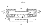
- a probe device 130 As a related-art probe device that solves the problem, there is a probe device 130 as shown in Fig. 2.
- Fig. 2 is a cross-sectional view showing a principal part of the related-art probe device.
- the related-art probe device 130 includes a stage 131, a first heater 132, a probe card holder 135, a probe card 136 and a second heater 137.
- the probe card holder 135 includes a probe card holding unit 141 and a heater holding unit 142.
- the probe card holding unit 141 is disposed above the stage 131.
- the probe card holding unit 141 is used to hold the probe card 136.
- the heater holding unit 142 is disposed on the probe card holding unit 141 and is configured integrally with the probe card holding unit 141.
- the heater holding unit 142 is used to hold the second heater 137.
- the probe card 136 is held in the probe card holding unit 141.
- the probe card 136 includes a probe pin 144 which is brought into contact with an external connection pad (not shown) of the semiconductor device 133 when the electrical inspection of the semiconductor device 133 is performed.
- the second heater 137 is held in the heater holding units 142.
- the second heater 137 heats the probe card 136 from a surface of the probe card 136 opposite a disposition surface of the probe pin 144.
- the second heater 137 is provided in the probe card holding unit 141 that is disposed above the probe card 136, and the probe card 136 is heated by the second heater 137 from the surface of the probe card 136 opposite the disposition surface of the probe pin 144. Therefore, it is possible to reduce deformation of the probe card 136 caused by the heat from the first heater 132. Accordingly, it is possible to measure electrical properties of the semiconductor device 133 heated to the predetermined temperature with high precision (see Japanese Unexamined Patent Application Publication No. 2000-138268 , for example).
- the related-art probe device 130 can measure the electrical properties of the semiconductor device 133 heated to a predetermined temperature with high precision, it is necessary to equip the heater holding unit 142 for holding the second heater 137, thus increasing the size of the probe device 130.
- a probe device according to independent claim 1 is provided. Further advantages, features, aspects and details are evident from the dependent claims, the description and the drawings.
- Exemplary embodiments of the present invention provide a probe device capable of measuring electrical properties of a semiconductor device that is heated to a predetermined temperature with high precision while reducing the size of the probe device.
- a probe device including: a stage for fixing a semiconductor device having an external connection pad; a heating unit provided in the stage, for heating the semiconductor device to a predetermined temperature; and a probe card having a probe pin and a support substrate for supporting the probe pin, in which the probe device performs an electrical inspection of the semiconductor device by bringing the probe pin in contact with the external connection pad of the semiconductor device heated to the predetermined temperature, and in which a resistance heating element is provided to the support substrate so as to heat a portion of the support substrate corresponding to a disposition portion of the probe pin to a temperature substantially equal to the predetermined temperature.
- the resistance heating element is provided to the support substrate so as to heat the portion of the support substrate corresponding to the disposition portion of the probe pin to a temperature substantially equal to the predetermined temperature (at which an electrical inspection of the semiconductor device is performed), it is possible to measure electrical properties of a semiconductor device that is heated to a predetermined temperature with high precision and to reduce the size of the probe device.
- a probe device capable of measuring electrical properties of a semiconductor device that is heated to a predetermined temperature with high precision while reducing the size of the probe device.
- Embodiments are also directed to methods by which the described apparatus operates. It may include method steps for carrying out functions of the apparatus. The method steps may be performed by way of hardware components, firmware, software, a computer programmed by appropriate software, by any combination thereof or in any other manner. Other features and advantages may be apparent from the following detailed description, the accompanying drawings and the claims.
- FIG. 3 is a cross-sectional view of an inspection apparatus according to a first embodiment of the invention.
- an X-X direction indicates a surface direction of a stage 17
- a Y-Y direction indicates a direction perpendicular to the surface direction of the stage 17.
- an inspection apparatus 10 includes a probe device 11 and a tester 12.
- the probe device 11 includes a casing 14, a drive unit 15, a support 16, the stage 17, a heating unit 18, a head plate 21, a holder support 22, a probe card holder 23, a probe card 24, a contact ring 25, a test head 26, a resistance heating element 27, a temperature detecting unit 28, a power supply 29 and a power control unit 30.
- the casing 14 houses the drive unit 15, the support 16 and the stage 17. An upper end of the casing 14 is formed as an opening end.
- the drive unit 15 is provided at a bottom 14A of the casing 14.
- the drive unit 15 is used to move the stage 17 in the X-X and Y-Y directions by means of the support 16.
- the support 16 is provided on the drive unit 15.
- the support 16 is used to movably support the stage 17.
- the stage 17 is fixed to an upper end of the support 16.
- the stage 17 is used to fix a semiconductor device 20.
- the semiconductor device 20 is disposed on a top surface 17A of the stage 17.
- the stage 17 moves integrally with the support 16 when the support 16 is moved by the drive unit 15.
- Fig. 4 is a cross-sectional view of a probe card that is electrically connected to an external connection pad of a semiconductor device.
- constituent elements identical to those of the inspection apparatus 10 according to the first embodiment are denoted by the same reference numerals.
- the semiconductor device 20 includes a semiconductor substrate 31 and a plurality of semiconductor integrated circuits 32.
- the semiconductor substrate 31 includes a plurality of circuit forming areas A in which the semiconductor integrated circuits 32 are formed.
- a Si substrate or a Ga-As substrate may be used as the semiconductor substrate 31, for example.
- the semiconductor integrated circuits 32 are disposed on portions of the semiconductor substrate 31 corresponding to the circuit forming areas A.
- the semiconductor integrated circuit 32 includes a diffusion layer (not shown), an insulating layer (not shown), a via-hole (not shown), a wiring (not shown), and an external connection pad 33 that is electrically connected to the diffusion layer, the via-hole and the wiring.
- the external connection pad 33 is formed on the uppermost layer of the semiconductor integrated circuit 32.
- the external connection pad 33 makes contact with a probe pin 48 that is provided in the probe card 24 when an electrical inspection of the semiconductor device 20 is performed.
- the heating unit 18 is incorporated in the stage 17.
- the heating unit 18 is used to heat the semiconductor device 20 via the stage 17 so that the temperature of the semiconductor device 20 reaches a predetermined temperature Tx.
- the predetermined temperature Tx represents the temperature at which a burn-in test (heating test) is performed for the semiconductor device 20.
- the predetermined temperature Tx may change depending on the type or inspection purpose of the semiconductor integrated circuit 32 that is provided in the semiconductor device 20, the temperature is set in the range of 90 °C to 150°C, for example.
- a heater may be used as the heating unit 18, for example.
- the head plate 21 includes a head plate body 35 and a contact ring mounting portion 36.
- the head plate 35 is provided on the casing 14.
- the head plate body 35 is configured so as to be open and closed with respect to the casing 14.
- the contact ring mounting portion 36 is configured to penetrate the vicinity of the central of the head plate body 35.
- the contact ring mounting portion 36 is used to mount the contact ring 25 on the head plate 21.
- a space C of the casing 14 is sealed when the heat plate 21 having the contact ring 25 mounted thereon covers the upper end of the casing 14.
- the holder support 22 is provided on a bottom surface 35A of the head plate body 35.
- the holder support 22 is used to support the probe card holder 23.
- the probe card holder 23 includes a holder body 38 and a probe card mounting portion 39.
- the holder body 38 is supported by the holder support 22.
- the probe card mounting portion 39 is configured to penetrate the holder body 38.
- the probe card mounting portion 39 is used to mount the probe card 24 on the probe card holder 23.
- the probe card 24 is disposed in the probe card mounting portion 39 and includes a support substrate 43, a through via-hole 44, an upper wiring 46, a lower wiring 47 and the probe pin 48.
- the support substrate 43 is formed in a board-like shape and has a plurality of through-holes 55.
- a material for the support substrate 43 a material having substantially the same thermal expansion coefficient as the semiconductor substrate 31 may be used. Specifically, when the Si substrate is used as the semiconductor substrate 31, Si may be used as the material for the support substrate 43.
- the support substrate 43 is formed of the material having substantially the same thermal expansion coefficient as the semiconductor substrate 31, it is possible to decrease a difference in thermal expansion coefficient between the probe card 24 and the semiconductor device 20. Accordingly, it is possible to reduce a contact failure between the probe pin 48 and the external connection pad 33.
- the through via-hole 44 is provided in the through-holes 55 formed on the support substrate 43.
- the upper end of the through via-hole 44 is connected to the upper wiring 46, and the lower end of the through via-hole 44 is connected to the lower wiring 47
- the upper wiring 46 is provided at a portion on a top surface 43A of the support substrate 43 corresponding to a disposition position of the through via-hole 44.
- the upper wiring 46 is connected to the upper end of the through via-hole 44.
- the lower wiring 47 is provided at a portion on a bottom surface 43B of the support substrate 43 corresponding to the disposition position of the through via-hole 44.
- the lower wiring 47 is connected to the lower end of the through via-hole 44.
- the lower wiring 47 is electrically connected to the upper wiring 46 via the through via-hole 44.
- the probe pin 48 is provided on the bottom surface 43B of the support substrate 43.
- the probe pin 48 is connected to the lower wiring 47. Accordingly, the probe pin 48 is electrically connected to the upper wiring 46 via the lower wiring 47 and the through via-hole 44.
- the probe card 24 is used as an inspection jig for pressing the probe pin 48 against the external connection pad 33 of the semiconductor integrated circuits 32 so that an electrical signal is inputted to the external connection pad 33.
- the contact ring 25 is detachably mounted on the contact ring mounting portion 36.
- the contact ring 25 includes a contact ring body 58, a first connection pin 61 and a second connection pin 62.
- the contact ring body 58 is electrically connected to the probe card 24 and the test head 26 via the first connection pin 61 and the second connection pin 62.
- the contact ring body 58 is used to transmit signals between the probe card 24 and the test head 26.
- the first connection pin 61 is disposed on a bottom surface 58B of the contact ring body 58.
- the first connection pin 61 protrudes out from the bottom surface 58B of the contact ring body 58.
- the end of the first connection pin 61 is electrically connected to the upper wiring 46 of the probe card 24.
- the second connection pin 62 is disposed on a top surface 58A of the contact ring body 58.
- the second connection pin 62 protrudes out from the top surface 58A of the contact ring body 58.
- the end of the second connection pin 62 protruding out from the top surface 58A of the contact ring body 58 is electrically connected to the test head 26.
- the second connection pin 62 is electrically connected to the first connection pin 61.
- the test head 26 is provided on the contact ring 25.
- the test head 26 is electrically connected to the tester 12.
- the test head 26 is used to receive inspection conditions of the semiconductor device 20 transmitted from the tester 12 and to transmit the inspection conditions to the probe card 24 via the contact ring 25.
- the resistance heating element 27 is provided on a portion of the bottom surface 43B of the support substrate 43, which is surrounded by the probe pin 48.
- Fig. 5 is a plan view of the resistance heating element.
- the resistance heating element 27 is formed of a wiring pattern (specifically, the resistance heating element is formed of a wiring pattern that is formed by patterning a metallic film).
- One end 27A of the resistance heating element 27 is electrically connected to a plus terminal 29A of the power supply 29 while the other end 27B of the resistance heating element 27 is electrically connected to a minus terminal 29B of the power supply 29.
- the resistance heating element 27 generates heat when supplied with power from the power supply 29.
- the resistance heating element 27 is used to heat a portion of the support substrate 43 corresponding to the disposition position of the probe pin 48 so that the temperature of the probe pin 48 is substantially equal to the predetermined temperature Tx (at which the electrical inspection of the semiconductor device 20 is performed).
- a metal having a high resistance value such as Ti or Ni may be used.
- the resistance heating element 27 may be formed using a method such as a subtractive process, a semi-additive process or a printing process.
- the support substrate 43 is heated so that the temperature at the portion of the support substrate 43 corresponding to the disposition position of the probe pin 48 reaches the predetermined temperature Tx (at which the electrical inspection of the semiconductor device 20 is performed). Therefore, it is possible to prevent the contact failure between the probe pin 48 (specifically, the front end of the probe pin 48 which makes contact with the external connection pad 33) and the external connection pad 33. Accordingly, it is possible to perform the electrical inspection of the semiconductor device 20 heated to the predetermined temperature Tx with high precision.
- the resistance heating element 27 is provided on the bottom surface 43B of the support substrate 43, it is possible to decrease the size of the probe device 10 compared with the related-art probe device 130 (see Fig. 2) in which the second heater 137 for heating the probe card 136 is provided at a position away from the probe card 136.
- the wiring pattern is used as the resistance heating element 27, it is possible to perform a process of forming the resistance heating element 27 as a part of and at the same time with the manufacturing process of the probe card 24.
- the temperature detecting unit 28 is provided in the vicinity of the center of the top surface 43A of the support substrate 43.
- the temperature detecting unit 28 is electrically connected to the power supply 29 (not shown).
- the temperature detecting unit 28 is used to detect the temperature at the portion of the support substrate 43 corresponding to the disposition position of the probe pin 48.
- the temperature detecting unit 28 transmits data on the detected temperature of the substrate 43 to the power control unit 30.
- a temperature sensor may be used as the temperature detecting unit 28, for example.
- the power supply 29 is electrically connected to the resistance heating element 27 and the power control unit 30.
- the power supply 29 includes the plus terminal 29A and the minus terminal 29B.
- the plus terminal 29A is electrically connected to the one end 27A of the resistance heating element 27 while the minus terminal 29B is electrically connected to the other end 27B of the resistance heating element 27.
- the power supply 29 is used to supply power to the resistance heating element 27 so that the resistance heating element 27 generates heat.
- the power control unit 30 is electrically connected to the temperature detecting unit 28 and the power supply 29.
- the power control unit 30 is used to control the power supply 29 (specifically, to control the power that the power supply 29 supplies to the resistance heating element 27) so that the temperature at the portion of the support substrate 43 corresponding to the disposition portion of the probe pins 48 is substantially equal to the predetermined temperature Tx on the basis of the data on the temperature of the support substrate 43 transmitted from the temperature detecting unit 30.
- the probe device of the present embodiment is provided with the temperature detecting unit 28 that detects the temperature at the portion of the support substrate 43 corresponding to the disposition position of the probe pin 48 and is also provided with the power control unit 30 that controls the power applied to the resistance heating unit 27 on the basis of the temperature of the support substrate 43 detected by the temperature detecting unit 28, it is possible to control the temperature with high precision so that the temperature at the portion of the support substrate 43 corresponding to the disposition position of the probe pin 48 is substantially equal to the predetermined temperature Tx.
- the support substrate 43 is heated so that the temperature at the portion of the support substrate 43 corresponding to the disposition position of the probe pin 48 reaches the predetermined temperature Tx (at which the electrical inspection of the semiconductor device 20 is performed). Therefore, it is possible to prevent the contact failure between the probe pin 48 (specifically, the front end of the probe pin 48 which makes contact with the external connection pad 33) and the external connection pad 33. Accordingly, it is possible to perform the electrical inspection of the semiconductor device 20 heated to the predetermined temperature Tx with high precision.
- the disposition position of the resistance heating element 27 is not limited to the position shown in Fig. 3.
- the resistance heating element 27 may be disposed on the top surface 43A of the support substrate 43.
- Fig. 6 is a cross-sectional view of an inspection apparatus according to a second embodiment of the invention.
- constituent elements identical to those of the inspection apparatus 10 according to the first embodiment are denoted by the same reference numerals.
- an inspection apparatus 70 according to the second embodiment is configured similar to the inspection apparatus 10 except that a probe device 71 is provided in the inspection apparatus 70 of the second embodiment instead of the probe device 11 of the inspection apparatus 10 of the first embodiment.
- the probe device 71 is configured similar to the probe device 11 except that a resistance heating element 73 is further provided in the probe device 71 of the second embodiment in addition the configuration of the probe device 11 of the first embodiment.
- Fig. 7 is a plan view of a resistance heating element provided on a top surface of a support substrate.
- the resistance heating element 73 is provided on the top surface 43A of the support substrate 43 located substantially in the vicinity of the center of the support substrate 43.
- the resistance heating element 73 is the wiring pattern formed by patterning the metallic film.
- One end 73A of the resistance heating element 73 is electrically connected to the plus terminal 29A of the power supply 29 and the other end 73B of the resistance heating element 73 is electrically connected to the minus terminal 29B of the power supply 29.
- the resistance heating element 73 generates heat when supplied with power from the power supply 29.
- the resistance heating element 73 is used to heat the support substrate 43 so that the temperature at the portions of the support substrate corresponding to the disposition portion of the probe pin 48 is substantially equal to the predetermined temperature Tx (at which the electrical inspection of the semiconductor device 20 is performed).
- a material for the resistance heating element 73 a metal such as Ti or Ni having the high resistance value may be used.
- the resistance heating element 73 may be formed using a method such as a subtractive process, a semi-additive process or a printing process.
- the probe device by providing the resistance heating element 27 on the bottom surface 43B of the support substrate 43 and providing the resistance heating element 73 on the top surface 43A of the support substrate 43, thereby heating the portion of the support substrate 43 corresponding to the disposition portion of the probe pin 48 from both sides of the support substrate, it is possible to prevent the deformation of the portion of the support substrate 43 corresponding to the disposition portion of the probe pin 48.
- the contact failure between the probe pin 48 specifically, the front end of the probe pin 48 which makes contact with the external connection pad 33
- the external connection pad 33 thus to perform the electrical inspection of the semiconductor device 20 heated to the predetermined temperature Tx with high precision.
- the resistance heating elements 27 and 73 are provided to the support substrate 43, it is possible to decrease the size of the probe device 70 compared with the related-art probe device 130 (see Fig. 2) in which the second heater 137 is provided at a position away from the probe card 136.
- a probe device includes a stage for fixing a semiconductor device having an external connection pad; a heating unit provided in the stage, for heating the semiconductor device to a predetermined temperature; and a probe card having a probe pin and a support substrate for supporting the probe pin, in which a resistance heating element is provided to the support substrate so as to heat a portion of the support substrate corresponding to a disposition portion of the probe pin to a temperature substantially equal to the predetermined temperature.
Landscapes
- Engineering & Computer Science (AREA)
- Environmental & Geological Engineering (AREA)
- Health & Medical Sciences (AREA)
- Toxicology (AREA)
- Computer Hardware Design (AREA)
- Microelectronics & Electronic Packaging (AREA)
- General Engineering & Computer Science (AREA)
- Physics & Mathematics (AREA)
- General Physics & Mathematics (AREA)
- Testing Or Measuring Of Semiconductors Or The Like (AREA)
- Tests Of Electronic Circuits (AREA)
- Measuring Leads Or Probes (AREA)
Abstract
Description
- This application claims priority to
Japanese Patent Application No. 2006-314568, filed November 21, 2006 - The present disclosure relates to a probe device, and more particularly, to a probe device for performing an electrical inspection of a semiconductor device heated to a predetermined temperature. More specifically, it relates to probe device.
- An electrical inspection of a semiconductor device including a semiconductor substrate having a plurality of chip forming areas and a semiconductor integrated circuit formed in the plurality of chip forming areas of the semiconductor substrate and having an external connection pad is performed by an inspection apparatus equipped with a tester and a probe device electrically connected to the tester.
- Fig. 1 is a cross-sectional view of a related-art inspection apparatus. In Fig. 1, an X1-X1 direction indicates a surface direction of a
stage 107, and a Y1-Y1 direction indicates a direction perpendicular to the surface direction of thestage 107. - Referring to Fig. 1, a related-
art inspection apparatus 100 includes aprobe device 101 and atester 102. Theprobe device 101 includes acasing 105, ahead plate 106, thestage 107, aheating unit 108, aprobe card holder 111, aprobe card 112, acontact ring 113 and atest head 114. - The
casing 105 houses thestage 107. The upper end of thecasing 105 is formed as an opening end. Thehead plate 106 is used to hold thecontact ring 113. Thehead plate 106 covers the upper end of thecasing 105 to seal an interior space of thecasing 105. - The
stage 107 is used to fix asemiconductor device 110. Thestage 107 is configured to be movable in the X1-X1 and Y1-Y1 directions. - The
heating unit 108 is incorporated in thestage 107. Theheating unit 108 is used to heat thesemiconductor device 110 via thestage 107 to a predetermined temperature (at which an electrical inspection of thesemiconductor device 110 is performed). Theprobe card holder 111 is used to hold theprobe card 112. - The
probe card 112 is held in theprobe card holder 111. Theprobe card 112 is disposed below thecontact ring 113. Theprobe card 112 includes asupport substrate 116, awiring pattern 117 and aprobe pin 118. Thesupport substrate 116 is formed in a board-like shape and has a through-hole for disposing a portion of thewiring pattern 117. Thesupport substrate 116 is a substrate for disposing thewiring pattern 117 and theprobe pin 118. - The
wiring pattern 117 penetrates thesupport substrate 116 so as to extend to bothsurfaces support substrate 116. The portion of thewiring pattern 117 disposed on thetop surface 116A of thesupport substrate 116 is electrically connected to thecontact ring 113. The portion of thewiring pattern 117 disposed on thebottom surface 116B of thesupport substrate 116 is connected to theprobe pin 118. Thewiring pattern 117 is used to electrically connect theprobe pin 118 to thecontact ring 113. - The
probe pin 118 is provided on thebottom surface 116B of thesupport substrate 116. Theprobe pin 118 is connected to thewiring pattern 117. Theprobe pin 118 is brought into contact with an external connection pad (not shown) provided in the semiconductor integrated circuit when the electrical inspection of thesemiconductor device 110 is performed. - The
contact ring 113 is held in thehead plate 106. Thecontact ring 113 is used to transmit an electrical signal between theprobe card 112 and thetest head 114 so that the electrical signal is communicated therebetween. - The
test head 114 is disposed on thecontact ring 113. Thetest head 114 is electrically connected to thecontact ring 113 and thetester 102. - The
tester 102 is electrically connected to thetest head 114. Thetester 102 controls an overall operation of theprobe device 101. Thetester 102 drives theprobe device 101 in accordance with a program previously stored in thetester 102. - The
inspection apparatus 100 having the above configuration performs the electrical inspection of the semiconductor device 110 (specifically, a plurality of semiconductor integrated circuits provided in the semiconductor device 110) in a state in which thesemiconductor device 110 is heated to the predetermined temperature by theheating unit 108. - However, since the related-
art probe device 101 is configured to heat thesemiconductor device 110, thesemiconductor device 110 is thermally deformed and thus a relative positional relation between theprobe pin 118 and the external connection pad (not shown) of the semiconductor integrated circuit is changed. Therefore, a contact failure occurs between theprobe pin 118 and the external connection pad (not shown). Accordingly, it is difficult to perform the electrical inspection of thesemiconductor device 110. with high precision. Such a problem becomes more likely when performing the electrical inspection is performed of a semiconductor device having a miniaturized semiconductor integrated circuit. - As a related-art probe device that solves the problem, there is a
probe device 130 as shown in Fig. 2. - Fig. 2 is a cross-sectional view showing a principal part of the related-art probe device.
- Referring to Fig. 2, the related-
art probe device 130 includes astage 131, afirst heater 132, aprobe card holder 135, aprobe card 136 and asecond heater 137. - The
first heater 132 is incorporated in thestage 131 for fixing asemiconductor device 133. Thefirst heater 132 is a heater for heating thesemiconductor substrate 133 to a predetermined temperature (at which the electrical inspection of thesemiconductor substrate 133 is performed). - The
probe card holder 135 includes a probecard holding unit 141 and aheater holding unit 142. The probecard holding unit 141 is disposed above thestage 131. The probecard holding unit 141 is used to hold theprobe card 136. Theheater holding unit 142 is disposed on the probecard holding unit 141 and is configured integrally with the probecard holding unit 141. Theheater holding unit 142 is used to hold thesecond heater 137. - The
probe card 136 is held in the probecard holding unit 141. Theprobe card 136 includes aprobe pin 144 which is brought into contact with an external connection pad (not shown) of thesemiconductor device 133 when the electrical inspection of thesemiconductor device 133 is performed. - The
second heater 137 is held in theheater holding units 142. Thesecond heater 137 heats theprobe card 136 from a surface of theprobe card 136 opposite a disposition surface of theprobe pin 144. - As described above, the
second heater 137 is provided in the probecard holding unit 141 that is disposed above theprobe card 136, and theprobe card 136 is heated by thesecond heater 137 from the surface of theprobe card 136 opposite the disposition surface of theprobe pin 144. Therefore, it is possible to reduce deformation of theprobe card 136 caused by the heat from thefirst heater 132. Accordingly, it is possible to measure electrical properties of thesemiconductor device 133 heated to the predetermined temperature with high precision (seeJapanese Unexamined Patent Application Publication No. 2000-138268 - Although the related-
art probe device 130 can measure the electrical properties of thesemiconductor device 133 heated to a predetermined temperature with high precision, it is necessary to equip theheater holding unit 142 for holding thesecond heater 137, thus increasing the size of theprobe device 130.
In light of the above, a probe device according toindependent claim 1 is provided.
Further advantages, features, aspects and details are evident from the dependent claims, the description and the drawings. - Exemplary embodiments of the present invention provide a probe device capable of measuring electrical properties of a semiconductor device that is heated to a predetermined temperature with high precision while reducing the size of the probe device.
- According to an aspect of the invention, there is provided a probe device including: a stage for fixing a semiconductor device having an external connection pad; a heating unit provided in the stage, for heating the semiconductor device to a predetermined temperature; and a probe card having a probe pin and a support substrate for supporting the probe pin, in which the probe device performs an electrical inspection of the semiconductor device by bringing the probe pin in contact with the external connection pad of the semiconductor device heated to the predetermined temperature, and in which a resistance heating element is provided to the support substrate so as to heat a portion of the support substrate corresponding to a disposition portion of the probe pin to a temperature substantially equal to the predetermined temperature.
- According to above aspect of the invention, since the resistance heating element is provided to the support substrate so as to heat the portion of the support substrate corresponding to the disposition portion of the probe pin to a temperature substantially equal to the predetermined temperature (at which an electrical inspection of the semiconductor device is performed), it is possible to measure electrical properties of a semiconductor device that is heated to a predetermined temperature with high precision and to reduce the size of the probe device.
- According to the invention, it is possible to provide a probe device capable of measuring electrical properties of a semiconductor device that is heated to a predetermined temperature with high precision while reducing the size of the probe device.
Embodiments are also directed to methods by which the described apparatus operates. It may include method steps for carrying out functions of the apparatus. The method steps may be performed by way of hardware components, firmware, software, a computer programmed by appropriate software, by any combination thereof or in any other manner.
Other features and advantages may be apparent from the following detailed description, the accompanying drawings and the claims. -
- Fig. 1 is a cross-sectional view of a related-art inspection device.
- Fig. 2 is a cross-sectional view of a principal part of the related-art probe device.
- Fig. 3 is a cross-sectional view of an inspection apparatus according to a first embodiment of the invention.
- Fig. 4 is a cross-sectional view of a probe card that is electrically connected to an external connection pad of a semiconductor device.
- Fig. 5 is a plan view of a resistance heating element.
- Fig. 6 is a cross-sectional view of an inspection apparatus according to a second embodiment of the invention.
- Fig. 7 is a plan view of a resistance heating element provided on a top surface of a support substrate.
- Next, embodiments of the invention will be described with reference to the accompanying drawings.
Fig. 3 is a cross-sectional view of an inspection apparatus according to a first embodiment of the invention. In Fig. 3, an X-X direction indicates a surface direction of astage 17, and a Y-Y direction indicates a direction perpendicular to the surface direction of thestage 17. - Referring to Fig. 1, an
inspection apparatus 10 according to the first embodiment of the invention includes aprobe device 11 and atester 12. Theprobe device 11 includes acasing 14, adrive unit 15, asupport 16, thestage 17, aheating unit 18, ahead plate 21, aholder support 22, aprobe card holder 23, aprobe card 24, acontact ring 25, atest head 26, aresistance heating element 27, atemperature detecting unit 28, apower supply 29 and apower control unit 30. - The casing 14 houses the
drive unit 15, thesupport 16 and thestage 17. An upper end of thecasing 14 is formed as an opening end. - The
drive unit 15 is provided at a bottom 14A of thecasing 14. Thedrive unit 15 is used to move thestage 17 in the X-X and Y-Y directions by means of thesupport 16. Thesupport 16 is provided on thedrive unit 15. Thesupport 16 is used to movably support thestage 17. - The
stage 17 is fixed to an upper end of thesupport 16. Thestage 17 is used to fix asemiconductor device 20. Thesemiconductor device 20 is disposed on atop surface 17A of thestage 17. Thestage 17 moves integrally with thesupport 16 when thesupport 16 is moved by thedrive unit 15. - Fig. 4 is a cross-sectional view of a probe card that is electrically connected to an external connection pad of a semiconductor device. In Fig. 4, constituent elements identical to those of the
inspection apparatus 10 according to the first embodiment are denoted by the same reference numerals. - Here, a configuration of the
semiconductor device 20 of which the electrical inspection is performed by theinspection apparatus 10 will be described with reference to Fig. 4. Thesemiconductor device 20 includes asemiconductor substrate 31 and a plurality of semiconductor integratedcircuits 32. Thesemiconductor substrate 31 includes a plurality of circuit forming areas A in which the semiconductor integratedcircuits 32 are formed. A Si substrate or a Ga-As substrate may be used as thesemiconductor substrate 31, for example. - The semiconductor integrated
circuits 32 are disposed on portions of thesemiconductor substrate 31 corresponding to the circuit forming areas A. The semiconductor integratedcircuit 32 includes a diffusion layer (not shown), an insulating layer (not shown), a via-hole (not shown), a wiring (not shown), and anexternal connection pad 33 that is electrically connected to the diffusion layer, the via-hole and the wiring. - The
external connection pad 33 is formed on the uppermost layer of the semiconductor integratedcircuit 32. Theexternal connection pad 33 makes contact with aprobe pin 48 that is provided in theprobe card 24 when an electrical inspection of thesemiconductor device 20 is performed. - Referring to Fig. 3, the
heating unit 18 is incorporated in thestage 17. Theheating unit 18 is used to heat thesemiconductor device 20 via thestage 17 so that the temperature of thesemiconductor device 20 reaches a predetermined temperature Tx. The predetermined temperature Tx represents the temperature at which a burn-in test (heating test) is performed for thesemiconductor device 20. Although the predetermined temperature Tx may change depending on the type or inspection purpose of the semiconductor integratedcircuit 32 that is provided in thesemiconductor device 20, the temperature is set in the range of 90 °C to 150°C, for example. A heater may be used as theheating unit 18, for example. - The
head plate 21 includes ahead plate body 35 and a contactring mounting portion 36. Thehead plate 35 is provided on thecasing 14. Thehead plate body 35 is configured so as to be open and closed with respect to thecasing 14. The contactring mounting portion 36 is configured to penetrate the vicinity of the central of thehead plate body 35. The contactring mounting portion 36 is used to mount thecontact ring 25 on thehead plate 21. A space C of thecasing 14 is sealed when theheat plate 21 having thecontact ring 25 mounted thereon covers the upper end of thecasing 14. - The
holder support 22 is provided on abottom surface 35A of thehead plate body 35. Theholder support 22 is used to support theprobe card holder 23. - The
probe card holder 23 includes aholder body 38 and a probecard mounting portion 39. Theholder body 38 is supported by theholder support 22. The probecard mounting portion 39 is configured to penetrate theholder body 38. The probecard mounting portion 39 is used to mount theprobe card 24 on theprobe card holder 23. - Referring to Figs. 3 and 4, the
probe card 24 is disposed in the probecard mounting portion 39 and includes asupport substrate 43, a through via-hole 44, anupper wiring 46, alower wiring 47 and theprobe pin 48. - The
support substrate 43 is formed in a board-like shape and has a plurality of through-holes 55. As a material for thesupport substrate 43, a material having substantially the same thermal expansion coefficient as thesemiconductor substrate 31 may be used. Specifically, when the Si substrate is used as thesemiconductor substrate 31, Si may be used as the material for thesupport substrate 43. - As described above, since the
support substrate 43 is formed of the material having substantially the same thermal expansion coefficient as thesemiconductor substrate 31, it is possible to decrease a difference in thermal expansion coefficient between theprobe card 24 and thesemiconductor device 20. Accordingly, it is possible to reduce a contact failure between theprobe pin 48 and theexternal connection pad 33. - The through via-
hole 44 is provided in the through-holes 55 formed on thesupport substrate 43. The upper end of the through via-hole 44 is connected to theupper wiring 46, and the lower end of the through via-hole 44 is connected to thelower wiring 47 - The
upper wiring 46 is provided at a portion on atop surface 43A of thesupport substrate 43 corresponding to a disposition position of the through via-hole 44. Theupper wiring 46 is connected to the upper end of the through via-hole 44. Thelower wiring 47 is provided at a portion on abottom surface 43B of thesupport substrate 43 corresponding to the disposition position of the through via-hole 44. Thelower wiring 47 is connected to the lower end of the through via-hole 44. Thelower wiring 47 is electrically connected to theupper wiring 46 via the through via-hole 44. - The
probe pin 48 is provided on thebottom surface 43B of thesupport substrate 43. Theprobe pin 48 is connected to thelower wiring 47. Accordingly, theprobe pin 48 is electrically connected to theupper wiring 46 via thelower wiring 47 and the through via-hole 44. Theprobe card 24 is used as an inspection jig for pressing theprobe pin 48 against theexternal connection pad 33 of the semiconductor integratedcircuits 32 so that an electrical signal is inputted to theexternal connection pad 33. - The
contact ring 25 is detachably mounted on the contactring mounting portion 36. Thecontact ring 25 includes acontact ring body 58, afirst connection pin 61 and asecond connection pin 62. Thecontact ring body 58 is electrically connected to theprobe card 24 and thetest head 26 via thefirst connection pin 61 and thesecond connection pin 62. Thecontact ring body 58 is used to transmit signals between theprobe card 24 and thetest head 26. - The
first connection pin 61 is disposed on abottom surface 58B of thecontact ring body 58. Thefirst connection pin 61 protrudes out from thebottom surface 58B of thecontact ring body 58. The end of thefirst connection pin 61 is electrically connected to theupper wiring 46 of theprobe card 24. - The
second connection pin 62 is disposed on atop surface 58A of thecontact ring body 58. Thesecond connection pin 62 protrudes out from thetop surface 58A of thecontact ring body 58. The end of thesecond connection pin 62 protruding out from thetop surface 58A of thecontact ring body 58 is electrically connected to thetest head 26. Thesecond connection pin 62 is electrically connected to thefirst connection pin 61. - The
test head 26 is provided on thecontact ring 25. Thetest head 26 is electrically connected to thetester 12. Thetest head 26 is used to receive inspection conditions of thesemiconductor device 20 transmitted from thetester 12 and to transmit the inspection conditions to theprobe card 24 via thecontact ring 25. - The
resistance heating element 27 is provided on a portion of thebottom surface 43B of thesupport substrate 43, which is surrounded by theprobe pin 48. - Fig. 5 is a plan view of the resistance heating element.
- Referring to Fig. 5, the
resistance heating element 27 is formed of a wiring pattern (specifically, the resistance heating element is formed of a wiring pattern that is formed by patterning a metallic film). Oneend 27A of theresistance heating element 27 is electrically connected to aplus terminal 29A of thepower supply 29 while theother end 27B of theresistance heating element 27 is electrically connected to a minus terminal 29B of thepower supply 29. Theresistance heating element 27 generates heat when supplied with power from thepower supply 29. Theresistance heating element 27 is used to heat a portion of thesupport substrate 43 corresponding to the disposition position of theprobe pin 48 so that the temperature of theprobe pin 48 is substantially equal to the predetermined temperature Tx (at which the electrical inspection of thesemiconductor device 20 is performed). As a material for theresistance heating element 27, a metal having a high resistance value such as Ti or Ni may be used. When Ni is used as the material for theresistance heating element 27, theresistance heating element 27 may be formed using a method such as a subtractive process, a semi-additive process or a printing process. - As described above, since the
resistance heating element 27 is disposed on thebottom surface 43B of thesupport substrate 43, thesupport substrate 43 is heated so that the temperature at the portion of thesupport substrate 43 corresponding to the disposition position of theprobe pin 48 reaches the predetermined temperature Tx (at which the electrical inspection of thesemiconductor device 20 is performed). Therefore, it is possible to prevent the contact failure between the probe pin 48 (specifically, the front end of theprobe pin 48 which makes contact with the external connection pad 33) and theexternal connection pad 33. Accordingly, it is possible to perform the electrical inspection of thesemiconductor device 20 heated to the predetermined temperature Tx with high precision. - Since the
resistance heating element 27 is provided on thebottom surface 43B of thesupport substrate 43, it is possible to decrease the size of theprobe device 10 compared with the related-art probe device 130 (see Fig. 2) in which thesecond heater 137 for heating theprobe card 136 is provided at a position away from theprobe card 136. - Since the wiring pattern is used as the
resistance heating element 27, it is possible to perform a process of forming theresistance heating element 27 as a part of and at the same time with the manufacturing process of theprobe card 24. - Referring to Fig. 3, the
temperature detecting unit 28 is provided in the vicinity of the center of thetop surface 43A of thesupport substrate 43. Thetemperature detecting unit 28 is electrically connected to the power supply 29 (not shown). Thetemperature detecting unit 28 is used to detect the temperature at the portion of thesupport substrate 43 corresponding to the disposition position of theprobe pin 48. Thetemperature detecting unit 28 transmits data on the detected temperature of thesubstrate 43 to thepower control unit 30. A temperature sensor may be used as thetemperature detecting unit 28, for example. - Referring to Fig. 3, the
power supply 29 is electrically connected to theresistance heating element 27 and thepower control unit 30. Thepower supply 29 includes theplus terminal 29A and theminus terminal 29B. Referring to Fig. 5, theplus terminal 29A is electrically connected to the oneend 27A of theresistance heating element 27 while theminus terminal 29B is electrically connected to theother end 27B of theresistance heating element 27. Thepower supply 29 is used to supply power to theresistance heating element 27 so that theresistance heating element 27 generates heat. - Referring to Fig. 3, the
power control unit 30 is electrically connected to thetemperature detecting unit 28 and thepower supply 29. Thepower control unit 30 is used to control the power supply 29 (specifically, to control the power that thepower supply 29 supplies to the resistance heating element 27) so that the temperature at the portion of thesupport substrate 43 corresponding to the disposition portion of the probe pins 48 is substantially equal to the predetermined temperature Tx on the basis of the data on the temperature of thesupport substrate 43 transmitted from thetemperature detecting unit 30. - As described above, since the probe device of the present embodiment is provided with the
temperature detecting unit 28 that detects the temperature at the portion of thesupport substrate 43 corresponding to the disposition position of theprobe pin 48 and is also provided with thepower control unit 30 that controls the power applied to theresistance heating unit 27 on the basis of the temperature of thesupport substrate 43 detected by thetemperature detecting unit 28, it is possible to control the temperature with high precision so that the temperature at the portion of thesupport substrate 43 corresponding to the disposition position of theprobe pin 48 is substantially equal to the predetermined temperature Tx. - In the probe device according to the present embodiment, since the
resistance heating element 27 is provided on thebottom surface 43B of thesupport substrate 43, thesupport substrate 43 is heated so that the temperature at the portion of thesupport substrate 43 corresponding to the disposition position of theprobe pin 48 reaches the predetermined temperature Tx (at which the electrical inspection of thesemiconductor device 20 is performed). Therefore, it is possible to prevent the contact failure between the probe pin 48 (specifically, the front end of theprobe pin 48 which makes contact with the external connection pad 33) and theexternal connection pad 33. Accordingly, it is possible to perform the electrical inspection of thesemiconductor device 20 heated to the predetermined temperature Tx with high precision. - Since the
resistance heating element 27 is provided on thebottom surface 43B of thesupport substrate 43, it is possible to decrease the size of theprobe device 10 compared with the related-art probe device 130 (see Fig. 2) in which thesecond heater 137 for heating theprobe card 136 is provided at a position away from theprobe card 136. - In the present embodiment, the disposition position of the
resistance heating element 27 is not limited to the position shown in Fig. 3. For example, theresistance heating element 27 may be disposed on thetop surface 43A of thesupport substrate 43. - The disposition position of the
temperature detecting unit 28 is not limited to the position shown in Fig. 3. For example, thetemperature detecting unit 28 may be disposed on thebottom surface 43B of thesupport substrate 43. - Fig. 6 is a cross-sectional view of an inspection apparatus according to a second embodiment of the invention. In Fig. 6, constituent elements identical to those of the
inspection apparatus 10 according to the first embodiment are denoted by the same reference numerals. - Referring to Fig. 6, an
inspection apparatus 70 according to the second embodiment is configured similar to theinspection apparatus 10 except that aprobe device 71 is provided in theinspection apparatus 70 of the second embodiment instead of theprobe device 11 of theinspection apparatus 10 of the first embodiment. - The
probe device 71 is configured similar to theprobe device 11 except that aresistance heating element 73 is further provided in theprobe device 71 of the second embodiment in addition the configuration of theprobe device 11 of the first embodiment. - Fig. 7 is a plan view of a resistance heating element provided on a top surface of a support substrate.
- Referring to Figs. 6 and 7, the
resistance heating element 73 is provided on thetop surface 43A of thesupport substrate 43 located substantially in the vicinity of the center of thesupport substrate 43. Theresistance heating element 73 is the wiring pattern formed by patterning the metallic film. Oneend 73A of theresistance heating element 73 is electrically connected to theplus terminal 29A of thepower supply 29 and theother end 73B of theresistance heating element 73 is electrically connected to the minus terminal 29B of thepower supply 29. Theresistance heating element 73 generates heat when supplied with power from thepower supply 29. Theresistance heating element 73 is used to heat thesupport substrate 43 so that the temperature at the portions of the support substrate corresponding to the disposition portion of theprobe pin 48 is substantially equal to the predetermined temperature Tx (at which the electrical inspection of thesemiconductor device 20 is performed). As a material for theresistance heating element 73, a metal such as Ti or Ni having the high resistance value may be used. When Ni is used as the material for theresistance heating element 73, theresistance heating element 73 may be formed using a method such as a subtractive process, a semi-additive process or a printing process. - In the probe device according to the present embodiment, by providing the
resistance heating element 27 on thebottom surface 43B of thesupport substrate 43 and providing theresistance heating element 73 on thetop surface 43A of thesupport substrate 43, thereby heating the portion of thesupport substrate 43 corresponding to the disposition portion of theprobe pin 48 from both sides of the support substrate, it is possible to prevent the deformation of the portion of thesupport substrate 43 corresponding to the disposition portion of theprobe pin 48. With this configuration, it is possible to prevent the contact failure between the probe pin 48 (specifically, the front end of theprobe pin 48 which makes contact with the external connection pad 33) and theexternal connection pad 33 and thus to perform the electrical inspection of thesemiconductor device 20 heated to the predetermined temperature Tx with high precision. - Since the
resistance heating elements support substrate 43, it is possible to decrease the size of theprobe device 70 compared with the related-art probe device 130 (see Fig. 2) in which thesecond heater 137 is provided at a position away from theprobe card 136. - The disposition position of the
resistance heating element 73 is not limited to the position shown in Fig. 6. - According to some embodiment described herein, a probe device includes a stage for fixing a semiconductor device having an external connection pad; a heating unit provided in the stage, for heating the semiconductor device to a predetermined temperature; and a probe card having a probe pin and a support substrate for supporting the probe pin, in which a resistance heating element is provided to the support substrate so as to heat a portion of the support substrate corresponding to a disposition portion of the probe pin to a temperature substantially equal to the predetermined temperature.
Hereinabove, although the preferred embodiments of the invention have been described and illustrated in detail, the invention is not limited to these specific embodiments and may be modified in various forms within the scope of the gist of the invention disclosed in the appended claims. - The invention can be applied to a probe device for measuring electrical properties of a semiconductor device heated to a predetermined temperature.
Claims (5)
- A probe device comprising:a stage (17) for fixing a semiconductor device (20) having an external connection pad (33);a heating unit (18) provided in the stage, for heating the semiconductor device to a predetermined temperature;a probe card (24) having a probe pin (48) and a support substrate (43) for supporting the probe pin, the probe pin being to be brought in contact with the external connection pad of the semiconductor device heated to the predetermined temperature when said probe device performs an electrical inspection of the semiconductor device; anda resistance heating element (27; 73) provided to the support substrate, for heating a portion of the support substrate corresponding to a disposition portion of the probe pin to a temperature substantially equal to the predetermined temperature.
- The probe device according to Claim 1, further comprising:a temperature detecting unit (28) provided in or on the support substrate, for detecting the temperature at the portion of the support substrate corresponding to the disposition portion of the probe pin; anda power control unit (30) for controlling a power that is applied to the resistance heating element so that the temperature detected by the temperature detecting unit is substantially equal to the predetermined temperature.
- The probe device according to Claim 1 or 2, wherein the resistance heating element (27; 73) is provided on a first surface of the support substrate (43) on which the probe pin is disposed and on a second surface of the support substrate opposite the first surface.
- The probe device according to any one of Claims 1 to 3, wherein the resistance heating element is a wiring pattern formed by patterning a metallic film.
- The probe device according to any one of Claims 1 to 4, wherein a thermal expansion efficient of the support substrate is substantially equal to that of the semiconductor device.
Applications Claiming Priority (1)
| Application Number | Priority Date | Filing Date | Title |
|---|---|---|---|
| JP2006314568A JP2008128838A (en) | 2006-11-21 | 2006-11-21 | Probe device |
Publications (2)
| Publication Number | Publication Date |
|---|---|
| EP1925945A2 true EP1925945A2 (en) | 2008-05-28 |
| EP1925945A3 EP1925945A3 (en) | 2011-04-27 |
Family
ID=39174214
Family Applications (1)
| Application Number | Title | Priority Date | Filing Date |
|---|---|---|---|
| EP07022621A Withdrawn EP1925945A3 (en) | 2006-11-21 | 2007-11-21 | Probe device with heating unit |
Country Status (5)
| Country | Link |
|---|---|
| US (1) | US7667474B2 (en) |
| EP (1) | EP1925945A3 (en) |
| JP (1) | JP2008128838A (en) |
| KR (1) | KR20080046093A (en) |
| TW (1) | TW200823472A (en) |
Cited By (1)
| Publication number | Priority date | Publication date | Assignee | Title |
|---|---|---|---|---|
| EP3012646A1 (en) * | 2014-10-21 | 2016-04-27 | STMicroelectronics Srl | Apparatus for the thermal testing of electronic devices and corresponding method |
Families Citing this family (29)
| Publication number | Priority date | Publication date | Assignee | Title |
|---|---|---|---|---|
| JP5074878B2 (en) * | 2007-10-15 | 2012-11-14 | 東京エレクトロン株式会社 | Inspection device |
| KR100977165B1 (en) | 2008-08-29 | 2010-08-20 | 주식회사 코리아 인스트루먼트 | Probe substrate and probe card having same |
| JP5199859B2 (en) * | 2008-12-24 | 2013-05-15 | 株式会社日本マイクロニクス | Probe card |
| JP5258547B2 (en) | 2008-12-26 | 2013-08-07 | 株式会社日本マイクロニクス | Integrated circuit inspection method and apparatus |
| JP5258590B2 (en) * | 2009-01-16 | 2013-08-07 | 株式会社日本マイクロニクス | Integrated circuit testing equipment |
| JP5535492B2 (en) * | 2009-02-12 | 2014-07-02 | ラピスセミコンダクタ株式会社 | Semiconductor integrated circuit inspection apparatus and semiconductor integrated circuit inspection method |
| KR101474951B1 (en) * | 2009-02-17 | 2014-12-24 | 삼성전자주식회사 | Apparatus for testing semiconductor device |
| JP5235163B2 (en) * | 2009-05-18 | 2013-07-10 | 株式会社日本マイクロニクス | Inspection device |
| US8400173B2 (en) * | 2009-06-26 | 2013-03-19 | Formfactor, Inc. | Method and apparatus for thermally conditioning probe cards |
| US8540422B2 (en) | 2010-10-04 | 2013-09-24 | Cameron Health, Inc. | Electrical component behavior analysis tools |
| JP5599341B2 (en) * | 2011-02-21 | 2014-10-01 | 株式会社シバソク | Test equipment |
| US8546904B2 (en) * | 2011-07-11 | 2013-10-01 | Transcend Information, Inc. | Integrated circuit with temperature increasing element and electronic system having the same |
| JP6031238B2 (en) * | 2012-03-09 | 2016-11-24 | 東京エレクトロン株式会社 | Wafer inspection interface and wafer inspection apparatus |
| TWM436227U (en) * | 2012-03-23 | 2012-08-21 | Mpi Corp | Heating point testing appliances |
| JP5861557B2 (en) * | 2012-04-26 | 2016-02-16 | 三菱電機株式会社 | Inspection device |
| US9316685B2 (en) * | 2012-11-12 | 2016-04-19 | Mpi Corporation | Probe card of low power loss |
| KR102077062B1 (en) | 2013-02-25 | 2020-02-13 | 삼성전자주식회사 | Probe card and apparatus for testing an object including the same |
| TWI481882B (en) * | 2013-04-12 | 2015-04-21 | Giga Byte Tech Co Ltd | Eletrical circuit board testing system and testing method thereof |
| JP6259590B2 (en) * | 2013-06-12 | 2018-01-10 | 株式会社日本マイクロニクス | Probe card and manufacturing method thereof |
| JP6041175B2 (en) * | 2015-03-30 | 2016-12-07 | 株式会社東京精密 | Prober |
| US11280827B2 (en) * | 2016-02-29 | 2022-03-22 | Teradyne, Inc. | Thermal control of a probe card assembly |
| JP6782103B2 (en) | 2016-06-21 | 2020-11-11 | 株式会社日本マイクロニクス | Probe card, inspection equipment and inspection method |
| JP7090517B2 (en) * | 2018-09-20 | 2022-06-24 | 東京エレクトロン株式会社 | Inspection equipment and inspection method |
| KR102023742B1 (en) * | 2019-01-31 | 2019-11-04 | (주)래딕스 | Test Pin Assembly |
| JP7345320B2 (en) * | 2019-04-25 | 2023-09-15 | 東京エレクトロン株式会社 | Temperature adjustment method for inspection equipment and probe card |
| KR102714625B1 (en) * | 2019-12-13 | 2024-10-11 | 산둥 차이쥐 일렉트로닉 테크놀로지 컴퍼니 리미티드 | Chip detection device, chip detection system and control method |
| JP7829278B2 (en) * | 2020-12-09 | 2026-03-13 | 東京エレクトロン株式会社 | Power supply and inspection equipment |
| JP2022096153A (en) * | 2020-12-17 | 2022-06-29 | 住友電気工業株式会社 | Electronic device inspection equipment and inspection method |
| TWI782443B (en) * | 2021-03-10 | 2022-11-01 | 陽榮科技股份有限公司 | Temperature control device for semiconductor testing |
Citations (2)
| Publication number | Priority date | Publication date | Assignee | Title |
|---|---|---|---|---|
| JP2000138268A (en) | 1998-11-04 | 2000-05-16 | Hitachi Chem Co Ltd | Inspection method and inspection device of semiconductor circuit |
| JP2006314568A (en) | 2005-05-13 | 2006-11-24 | Daiichi Shokai Co Ltd | Game machine |
Family Cites Families (13)
| Publication number | Priority date | Publication date | Assignee | Title |
|---|---|---|---|---|
| BE1000697A6 (en) * | 1987-10-28 | 1989-03-14 | Irish Transformers Ltd | Device for testing integrated electrical circuits. |
| US4839587A (en) * | 1988-03-29 | 1989-06-13 | Digital Equipment Corporation | Test fixture for tab circuits and devices |
| JPH0748946Y2 (en) * | 1989-06-30 | 1995-11-08 | コクヨ株式会社 | Moving partition device |
| US5124639A (en) * | 1990-11-20 | 1992-06-23 | Motorola, Inc. | Probe card apparatus having a heating element and process for using the same |
| JP3214766B2 (en) * | 1992-08-06 | 2001-10-02 | アジレント・テクノロジーズ・インク | Equipment for connection inspection |
| JPH0954116A (en) * | 1995-08-10 | 1997-02-25 | Nippon Denshi Zairyo Kk | High temperature probe card |
| US6690185B1 (en) * | 1997-01-15 | 2004-02-10 | Formfactor, Inc. | Large contactor with multiple, aligned contactor units |
| US6181145B1 (en) * | 1997-10-13 | 2001-01-30 | Matsushita Electric Industrial Co., Ltd. | Probe card |
| JP2000346875A (en) * | 1999-06-07 | 2000-12-15 | Advantest Corp | Probe card and IC testing device using the same |
| US7071714B2 (en) * | 2001-11-02 | 2006-07-04 | Formfactor, Inc. | Method and system for compensating for thermally induced motion of probe cards |
| JP4173306B2 (en) * | 2001-11-30 | 2008-10-29 | 東京エレクトロン株式会社 | Reliability evaluation test apparatus, reliability evaluation test system, and reliability evaluation test method |
| JP2004150999A (en) * | 2002-10-31 | 2004-05-27 | Advantest Corp | Probe card |
| US7495458B2 (en) * | 2006-05-17 | 2009-02-24 | Texas Instruments Incorporated | Probe card and temperature stabilizer for testing semiconductor devices |
-
2006
- 2006-11-21 JP JP2006314568A patent/JP2008128838A/en active Pending
-
2007
- 2007-11-08 KR KR1020070113563A patent/KR20080046093A/en not_active Withdrawn
- 2007-11-19 TW TW096143651A patent/TW200823472A/en unknown
- 2007-11-20 US US11/984,601 patent/US7667474B2/en not_active Expired - Fee Related
- 2007-11-21 EP EP07022621A patent/EP1925945A3/en not_active Withdrawn
Patent Citations (2)
| Publication number | Priority date | Publication date | Assignee | Title |
|---|---|---|---|---|
| JP2000138268A (en) | 1998-11-04 | 2000-05-16 | Hitachi Chem Co Ltd | Inspection method and inspection device of semiconductor circuit |
| JP2006314568A (en) | 2005-05-13 | 2006-11-24 | Daiichi Shokai Co Ltd | Game machine |
Cited By (2)
| Publication number | Priority date | Publication date | Assignee | Title |
|---|---|---|---|---|
| EP3012646A1 (en) * | 2014-10-21 | 2016-04-27 | STMicroelectronics Srl | Apparatus for the thermal testing of electronic devices and corresponding method |
| US10107856B2 (en) | 2014-10-21 | 2018-10-23 | Stmicroelectronics S.R.L. | Apparatus for the thermal testing of electronic devices and corresponding method |
Also Published As
| Publication number | Publication date |
|---|---|
| US20080116925A1 (en) | 2008-05-22 |
| EP1925945A3 (en) | 2011-04-27 |
| US7667474B2 (en) | 2010-02-23 |
| JP2008128838A (en) | 2008-06-05 |
| KR20080046093A (en) | 2008-05-26 |
| TW200823472A (en) | 2008-06-01 |
Similar Documents
| Publication | Publication Date | Title |
|---|---|---|
| US7667474B2 (en) | Probe device | |
| KR101018902B1 (en) | Test device | |
| JP4745060B2 (en) | Probe card | |
| JP2008051792A (en) | Integrated circuit probe apparatus having temperature control mechanism | |
| JPH0792479B2 (en) | Parallelism adjustment method for probe device | |
| KR102411561B1 (en) | Temperature measurement member, inspection apparatus, and temperature measurement method | |
| WO2006001476A1 (en) | Probe card | |
| JPWO2008146705A1 (en) | Probe card fixing device | |
| CN110931390B (en) | Inspection equipment and inspection methods | |
| JP2010186851A (en) | Testing apparatus and testing method of semiconductor integrated circuit | |
| JP2010243352A (en) | Probe card manufacturing method | |
| JP2003344498A (en) | Semiconductor test equipment | |
| CN114496838B (en) | Mounting table, inspection device, and inspection method | |
| WO2004040321A1 (en) | Probe card | |
| JP4560057B2 (en) | Electronic component inspection equipment | |
| JP2005228788A (en) | Method for aligning wafer and probe card, probe inspection method and probe inspection apparatus | |
| JP2009070874A (en) | Inspection device | |
| JP4598781B2 (en) | Electronic component inspection container | |
| TWI917459B (en) | Platform, inspection device and inspection method | |
| JP2007208138A (en) | Inspection method of semiconductor device | |
| JP2010038651A (en) | Probe card, element testing device, and element test method | |
| KR102890820B1 (en) | Probe card | |
| KR20140110440A (en) | Probing method, probe card for performing the method, and probing apparatus including the probe card | |
| JP2016194502A (en) | Burn-in test jig and burn-in test method | |
| CN114822674A (en) | Memory chip test seat and test device |
Legal Events
| Date | Code | Title | Description |
|---|---|---|---|
| PUAI | Public reference made under article 153(3) epc to a published international application that has entered the european phase |
Free format text: ORIGINAL CODE: 0009012 |
|
| AK | Designated contracting states |
Kind code of ref document: A2 Designated state(s): AT BE BG CH CY CZ DE DK EE ES FI FR GB GR HU IE IS IT LI LT LU LV MC MT NL PL PT RO SE SI SK TR |
|
| AX | Request for extension of the european patent |
Extension state: AL BA HR MK RS |
|
| PUAL | Search report despatched |
Free format text: ORIGINAL CODE: 0009013 |
|
| AK | Designated contracting states |
Kind code of ref document: A3 Designated state(s): AT BE BG CH CY CZ DE DK EE ES FI FR GB GR HU IE IS IT LI LT LU LV MC MT NL PL PT RO SE SI SK TR |
|
| AX | Request for extension of the european patent |
Extension state: AL BA HR MK RS |
|
| STAA | Information on the status of an ep patent application or granted ep patent |
Free format text: STATUS: THE APPLICATION IS DEEMED TO BE WITHDRAWN |
|
| AKY | No designation fees paid | ||
| REG | Reference to a national code |
Ref country code: DE Ref legal event code: R108 |
|
| 18D | Application deemed to be withdrawn |
Effective date: 20110601 |
|
| REG | Reference to a national code |
Ref country code: DE Ref legal event code: R108 Effective date: 20120104 |