EP1923785B1 - Alternatively reconfigurable fault tolerant computing architecture - Google Patents
Alternatively reconfigurable fault tolerant computing architecture Download PDFInfo
- Publication number
- EP1923785B1 EP1923785B1 EP07120941A EP07120941A EP1923785B1 EP 1923785 B1 EP1923785 B1 EP 1923785B1 EP 07120941 A EP07120941 A EP 07120941A EP 07120941 A EP07120941 A EP 07120941A EP 1923785 B1 EP1923785 B1 EP 1923785B1
- Authority
- EP
- European Patent Office
- Prior art keywords
- signal processing
- reconfigurable
- processing
- reconfiguration
- payload
- Prior art date
- Legal status (The legal status is an assumption and is not a legal conclusion. Google has not performed a legal analysis and makes no representation as to the accuracy of the status listed.)
- Not-in-force
Links
Images

Classifications
-
- G—PHYSICS
- G06—COMPUTING OR CALCULATING; COUNTING
- G06F—ELECTRIC DIGITAL DATA PROCESSING
- G06F11/00—Error detection; Error correction; Monitoring
- G06F11/07—Responding to the occurrence of a fault, e.g. fault tolerance
- G06F11/16—Error detection or correction of the data by redundancy in hardware
- G06F11/20—Error detection or correction of the data by redundancy in hardware using active fault-masking, e.g. by switching out faulty elements or by switching in spare elements
- G06F11/202—Error detection or correction of the data by redundancy in hardware using active fault-masking, e.g. by switching out faulty elements or by switching in spare elements where processing functionality is redundant
- G06F11/2023—Failover techniques
- G06F11/2025—Failover techniques using centralised failover control functionality
-
- G—PHYSICS
- G06—COMPUTING OR CALCULATING; COUNTING
- G06F—ELECTRIC DIGITAL DATA PROCESSING
- G06F11/00—Error detection; Error correction; Monitoring
- G06F11/07—Responding to the occurrence of a fault, e.g. fault tolerance
- G06F11/14—Error detection or correction of the data by redundancy in operations
- G06F11/1402—Saving, restoring, recovering or retrying
- G06F11/1415—Saving, restoring, recovering or retrying at system level
- G06F11/142—Reconfiguring to eliminate the error
Definitions
- FPGA field-programmable gate array
- WO 2006/052397 discloses an electronic system to accept various different environmental inputs from a sensor suite that can induce faults in a target computer, such as a payload computer system.
- the present invention provides a system as defined in Claim 1.
- the system may include the features of any one or more of dependent Claims 2 to 10.
- a method for reducing radiation effects in an electronic circuit involves periodically transferring operation of the electronic circuit to at least one alternate processing element of a plurality of processing elements. With the at least one alternate processing element in control, the method reconfigures one or more processing elements of the plurality of processing elements. Once the one or more processing elements are reconfigured, the method synchronizes the one or more processing elements with the at least one alternate processing element.
- FIG. 1 is a block diagram of an embodiment of an electronic system incorporating an alternating fault tolerant reconfigurable computing architecture
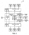
- FIG. 2 is a block diagram of an embodiment of a signal processing node within the system of FIG. 1 ;
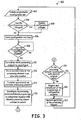
- FIG. 3 is a flow diagram illustrating an embodiment of a method for reducing radiation effects in the signal processing node of FIG. 2 .
- FIG. 1 is a block diagram of an embodiment of an electronic system 100.
- the system 100 comprises a signal processing unit 102, a payload interface block 104 responsive to the signal processing unit 102, and sensors 108 1 to 108 N coupled to the signal processing unit 102.
- the signal processing unit 102 further includes signal processing nodes 114 1 to 114 N , a payload control computer 110, a power supply unit 116, and a common interface bus 112.
- the common interface bus 112 is, without limitation, a compact peripheral component interconnect (cPCI) bus.
- each of the sensors 108 is individually coupled to a respective signal processing node 114.
- cPCI compact peripheral component interconnect
- each of the sensors 108 is, without limitation, at least one of a visible focal plane array, a guidance sensor, and an infrared focal plane array. It is understood that the system 100 is capable of accommodating any appropriate number and type of the sensors 108 1 to 108 N and the signal processing nodes 114 1 to 114N (for example, one or more sensors 108 coupled to one or more signal processing nodes 114 in a single signal processing unit 102) for communication with the payload interface block 104.
- a plurality of reconfigurable processing elements in each of the signal processing nodes 114 1 to 114 N periodically alternate between reconfiguration and signal processing to maintain operational time continuity of the signal processing unit 102.
- the periodic alternating reconfiguration substantially eliminates radiation effects on the signal processing unit 102, as discussed in further detail below with respect to FIG. 2 , by preventing an accumulation of radiation in the plurality of reconfigurable processing elements in each of the signal processing nodes 114 1 to 114 N .
- the sensors 108 1 to 108 N collect raw payload data (for example, spacecraft communications signals) for signal processing by the signal processing nodes 114 1 to 114 N .
- the payload interface block 104 receives the processed payload data from the signal processing nodes 114 1 to 114 N .
- The, at least one, payload control computer 110 communicates with the one or more signal processing nodes 114 1 to 114N over the common interface bus 112.
- the at least one payload control computer 110 also issues payload control commands to the payload interface block 104.
- the power supply unit 116 supplies a plurality of secondary power signals (voltages) to the signal processing nodes 114 1 to 114 N and to the at least one payload control computer 110 over the common interface bus 112.
- the signal processing nodes 114 1 to 114 N comprise symmetrical reconfigurable processing elements (that is, reconfigurable processing elements with comparable capabilities and features) that enhance mitigation efforts in the reduction of radiation effects on the signal processing unit 102.
- the signal processing nodes 114 1 to 114 N reconfigure each of the symmetrical reconfigurable processing elements (described in further detail below with respect to FIG. 2 ) to substantially eliminate radiation effects on the signal processing unit 102.
- computing availability of the signal processing nodes 114 1 to 114 N is based on a programmable alternating reconfiguration rate that substantially minimizes reconfiguration processing time.
- the alternating computing approach described here (including a programmable resynchronization timer) is implemented in the configuration management of the signal processing nodes 114 1 to 114 N (described in further detail below with respect to FIG. 2 ).
- FIG. 2 is a block diagram of an embodiment of a signal processing node 200 within the system 100.
- the signal processing node 200 represents one of the signal processing nodes 114 of FIG. 1 .
- the signal processing node 200 comprises a set of at least two processing elements 204 and 206, a sensor interface processor 202 in communication with the set of processing elements 204 and 206, and a configuration memory 208 in communication with the sensor interface processor 202.
- the configuration memory 208 comprises a single set of program logic files. In one or more alternate implementations, one or more sets of program logic files reside in the configuration memory 208.
- the memory controller 218 sequences a particular (unique) operation of the signal processing node 200 with the one or more sets of program logic files.
- the configuration manager 214 determines which of the program logic files within the configuration memory 208 to use in (re)configuring the processing elements 204 and 206.
- the signal processing node 200 further comprises local memories 205 1 to 205 M coupled to the processing element 204, and local memories 207 1 to 207 M coupled to the processing element 206.
- the processing element 204 is described in terms of a processing element A
- the processing element 206 is described in terms of a processing element B.
- the processing element A is functionally substantially identical with respect to the processing element B.
- Each of the processing elements A and B are, without limitation, any programmable logic devices including a field-programmable gate array (FPGA), a complex programmable logic device (CPLD), and a field-programmable object array (FPOA).
- FPGA field-programmable gate array
- CPLD complex programmable logic device
- FPOA field-programmable object array
- Each of the local memory devices 205 and 207 comprise, without limitation, at least one of quad data rate static random access memory (QDR SRAM) devices and dual data rate synchronous dynamic random access memory (DDR SDRAM) devices. It is understood that the signal processing node 200 is capable of accommodating any appropriate number of the processing elements 204 and 206 and corresponding local memories 205 1 to 205 M and 207 1 to 207 M , respectively (for example, one or more series of local memories 205 and 207 coupled to one or more sets of processing elements 204 and 206) in a single signal processing node 200.
- QDR SRAM quad data rate static random access memory
- DDR SDRAM dual data rate synchronous dynamic random access memory
- the sensor interface processor 202 processes sensor payload data from the one or more sensors 108 of FIG. 1 .
- the sensor interface processor 202 is a radiation hardened computing element (for example, an application-specific integrated circuit, or ASIC) that includes a configuration manager 214 to manage processing of the sensor payload data between the processing elements A and B.
- the configuration manager 214 further comprises a programmable timer 215 that signals the beginning of an alternate processing and reconfiguration interval.
- the sensor interface processor 202 further includes interprocessor network interfaces 220 1 to 220 2 and a memory controller 218.
- the interprocessor network interface 220 1 communicates with the payload control computer 110 (via the common interface bus 112), and the interprocessor network interface 220 2 is in communication with the payload interface block 104 of FIG. 1 .
- the memory controller 218 is in communication with the configuration manager 214 and the configuration memory 208.
- the signal processing node 200 further comprises alternate data buffers 210 and 212, each of the alternate data buffers 210 and 212 responsive to a data path control block 216.
- the alternate data buffer 210 (shown as alternate data buffer PEB) stores a current processing element state of the processing element B.
- the alternate data buffer 212 (shown as alternate data buffer PEA) stores a current processing element state of the processing element A.
- the data path control block 216 transfers the current processing element state from the local memory devices 205 1 to 205 M (207 1 to 207 M ) to the alternate data buffer 212 (210).
- the alternate data buffers 210 and 212 comprise, without limitation, at least one of QDR SRAM devices and DDR SDRAM devices.
- the alternate data buffer 210 (212) comprises equivalent memory storage capacity as that of the local memory devices 205 1 to 205 M (207 1 to 207 M ).
- the sensor interface processor 202 periodically alternates processing between the processing elements A and B.
- the configuration manager 214 reconfigures processing element A while processing element B continues to function.
- the memory controller 218 reconfigures one or more sets of processing logic from the configuration memory 208 between the processing elements A and B based on a programmable reconfiguration rate determined by the programmable timer 215.
- the data path control block 216 synchronizes operation of the processing elements A and B between alternating processing operations to substantially reduce radiation susceptibilities in the signal processing system of FIG. 1 .
- the data path control block 216 restores operation of a (reconfigured) processing element A (B) within 100 ms using the alternate data buffer PEA (PEB) assigned to the processing elements A and B, respectively.
- the sensor interface processor 202 periodically reconfigures at least a portion of the processing elements A and B in an alternating fashion such that while the processing element A (B) is processing the sensor payload data, the processing element B (A) is reconfigured and any radiation-induced upsets are removed.
- the signal processing node 200 utilizes the sensor interface processor 202 (specifically, the configuration manager 214, the programmable timer 215, and the alternate data buffers 210 and 212 to periodically alternate reconfiguration of the processing elements A and B so that at least one of the processing elements A (B) continues to process sensor payload data.
- the alternate data buffers 210 and 212 resynchronize the reconfigured processing element A (B) with the processing element B (A) by restoring a current state of each of the reconfigured processing elements A and B.
- Periodic and planned reconfiguration and resynchronization within the computing architecture of FIG. 2 substantially minimizes reconfiguration processing time.
- the reconfiguration processing time is less than 100 ms.
- FIG. 3 is a flow diagram illustrating a method 300 for reducing radiation effects in the signal processing unit 200 of FIG. 1 .
- the method 300 addresses periodically transferring operation of the signal processing node 200 to the processing element 206 (204) by exchanging current state information of the processing element 204 (206) with the processing element 206 (204).
- the configuration manager 214 stores the current state information of the processing element 204 (206) in the alternate data buffer 212 (210).
- the data path control block 216 recalls a current state of the processing elements 204 (206) prior to reconfiguration of the processing element 204 (206) by sequencing a loading of individual program logic files from the configuration memory 208.
- the configuration manager 214 alternates identical program logic files from the configuration memory 208 between the processing elements 204 and 206.
- the sensor interface processor 202 synchronizes the (now-reconfigured) processing element 204 (206) with the processing element 206 (204).
- the configuration manager 214 restores operation of the processing element 204 (206) within 100 ms.
- the configuration manager 214 evaluates the programmable reconfiguration rate in the programmable timer 215. If block 304 determines that the programmable reconfiguration rate has not been modified (alternatively, the reconfiguration rate is a fixed rate), the reconfiguration rate timer is started at block 306. If the programmable reconfiguration rate has been modified, the configuration manager 214 is updated at block 305. Once the reconfiguration rate timer expires (based on the programmable reconfiguration rate in the programmable timer 215) at block 308, the configuration manager 214 determines which of the processing elements of the signal processing node 200 to reconfigure at block 310. For example, if the processing element 204 was last reconfigured, the processing element 206 will be reconfigured.
- the data path control block 216 stores the current state of the processing element 206 in the alternate data buffer 210 at block 312.
- the configuration manager 214 transfers operation of the signal processing node 200 to the processing element 204.
- the configuration manager 214 reconfigures the processing element 206 with the latest program logic as indicated by the memory controller 218.
- the memory controller 218 transfers the latest program logic as one or more program logic files from the configuration memory 208.
- block 318 determines if the processing element 206 is being reconfigured with identical program logic as a previous reconfiguration of the processing element 206.
- the memory controller 218 prepares the next set of the latest program logic files in the configuration sequence of the signal processing node 200 at block 320.
- the configuration manager 214 restores operation of the processing element 206 by returning the current state information of the processing element 206 from the alternate data buffer 210.
- While the methods and techniques described here have been described in the context of a fully functioning fault tolerant signal processing unit (for example, the signal processing unit 102 of FIG. 1 ), apparatus embodying these techniques are capable of being distributed in the form of a computer readable medium of instructions and a variety of forms that apply equally regardless of the particular type of signal bearing media actually used to carry out the distribution.
- Examples of computer readable media include recordable-type media, such as a portable memory device, a hard disk drive, a RAM, CD-ROMs, DVD-ROMs, and transmission-type media, such as digital and analog communications links, wired or wireless communications links using transmission forms, such as, for example, radiofrequency (RF) and light wave transmissions.
- the computer readable media may take the form of coded formats that are decoded for actual use in a particular fault tolerant signal processing unit.
Landscapes
- Engineering & Computer Science (AREA)
- Theoretical Computer Science (AREA)
- Quality & Reliability (AREA)
- Physics & Mathematics (AREA)
- General Engineering & Computer Science (AREA)
- General Physics & Mathematics (AREA)
- Logic Circuits (AREA)
- Hardware Redundancy (AREA)
Description
- Present and future high-reliability (that is, space) missions require significant increases in on-board signal processing. Presently, generated data is not transmitted via downlink channels in a reasonable time. As users of the generated data demand faster access, increasingly more data reduction or feature extraction processing is performed directly on the high-reliability vehicle (for example, spacecraft) involved. Increasing processing power on the high-reliability vehicle provides an opportunity to narrow the bandwidth for the generated data and/or increase the number of independent user channels.
- In signal processing applications, traditional instruction-based processor approaches are unable to compete with million-gate, field-programmable gate array (FPGA)-based processing architectures. Systems with multiple FPGA-based processors are required to meet computing needs for Space Based Radar (SBR), next-generation adaptive beam forming, and adaptive modulation space-based communication programs. As the name implies, an FPGA-based system is easily reconfigured to meet new requirements. FPGA-based reconfigurable processing architectures are also re-useable and able to support multiple space-based communication programs with relatively simple changes to their unique data interfaces.
- Existing commercial-off-the-shelf (COTS), synchronous read-only memory (SRAM)-based processing elements are sensitive to radiation-induced upsets. Consequently, traditional COTS-based reconfigurable systems are unreliable in high-radiation environments. Furthermore, existing diagnostic approaches for detecting and mitigating susceptibilities to one or more single event upsets (SEUs), single event functional interrupts (SEFIs) and single event transients (SETs) have several disadvantages, particularly with respect to partial reconfiguration. Partial reconfiguration involves replacing (restoring) dynamic memory register contents with new (existing) processing configurations while leaving static memory register contents intact. Current methods of partial reconfiguration remove radiation effects in dynamic memory portions of the processing system while (potentially) leaving static memory portions with accumulated radiation over a significant time period.
- International Patent Specification Publication No.
WO 2006/052397 discloses an electronic system to accept various different environmental inputs from a sensor suite that can induce faults in a target computer, such as a payload computer system. - The present invention provides a system as defined in Claim 1.
The system may include the features of any one or more ofdependent Claims 2 to 10. - The following specification addresses an alternating fault tolerant reconfigurable computing architecture for electronic systems. Particularly, in one embodiment, a method for reducing radiation effects in an electronic circuit is provided. The method involves periodically transferring operation of the electronic circuit to at least one alternate processing element of a plurality of processing elements. With the at least one alternate processing element in control, the method reconfigures one or more processing elements of the plurality of processing elements. Once the one or more processing elements are reconfigured, the method synchronizes the one or more processing elements with the at least one alternate processing element.
- These and other features, aspects, and advantages will be better understood with regard to the following description, appended claims, and accompanying drawings where:
-
FIG. 1 is a block diagram of an embodiment of an electronic system incorporating an alternating fault tolerant reconfigurable computing architecture; -
FIG. 2 is a block diagram of an embodiment of a signal processing node within the system ofFIG. 1 ; and -
FIG. 3 is a flow diagram illustrating an embodiment of a method for reducing radiation effects in the signal processing node ofFIG. 2 . -
FIG. 1 is a block diagram of an embodiment of anelectronic system 100. Thesystem 100 comprises asignal processing unit 102, apayload interface block 104 responsive to thesignal processing unit 102, andsensors 1081 to 108N coupled to thesignal processing unit 102. Thesignal processing unit 102 further includessignal processing nodes 1141 to 114N, apayload control computer 110, apower supply unit 116, and acommon interface bus 112. In one implementation of thesystem 100, thecommon interface bus 112 is, without limitation, a compact peripheral component interconnect (cPCI) bus. In the same or alternate implementations, each of thesensors 108 is individually coupled to a respectivesignal processing node 114. In the example embodiment ofFIG. 1 , each of thesensors 108 is, without limitation, at least one of a visible focal plane array, a guidance sensor, and an infrared focal plane array. It is understood that thesystem 100 is capable of accommodating any appropriate number and type of thesensors 1081 to 108N and thesignal processing nodes 1141 to 114N (for example, one ormore sensors 108 coupled to one or moresignal processing nodes 114 in a single signal processing unit 102) for communication with thepayload interface block 104. - In operation, a plurality of reconfigurable processing elements in each of the
signal processing nodes 1141 to 114N periodically alternate between reconfiguration and signal processing to maintain operational time continuity of thesignal processing unit 102. The periodic alternating reconfiguration substantially eliminates radiation effects on thesignal processing unit 102, as discussed in further detail below with respect toFIG. 2 , by preventing an accumulation of radiation in the plurality of reconfigurable processing elements in each of thesignal processing nodes 1141 to 114N. Thesensors 1081 to 108N collect raw payload data (for example, spacecraft communications signals) for signal processing by thesignal processing nodes 1141 to 114N. Thepayload interface block 104 receives the processed payload data from thesignal processing nodes 1141 to 114N. The, at least one,payload control computer 110 communicates with the one or moresignal processing nodes 1141 to 114N over thecommon interface bus 112. The at least onepayload control computer 110 also issues payload control commands to thepayload interface block 104. Thepower supply unit 116 supplies a plurality of secondary power signals (voltages) to thesignal processing nodes 1141 to 114N and to the at least onepayload control computer 110 over thecommon interface bus 112. - The
signal processing nodes 1141 to 114N comprise symmetrical reconfigurable processing elements (that is, reconfigurable processing elements with comparable capabilities and features) that enhance mitigation efforts in the reduction of radiation effects on thesignal processing unit 102. Thesignal processing nodes 1141 to 114N reconfigure each of the symmetrical reconfigurable processing elements (described in further detail below with respect toFIG. 2 ) to substantially eliminate radiation effects on thesignal processing unit 102. In one implementation, computing availability of thesignal processing nodes 1141 to 114N is based on a programmable alternating reconfiguration rate that substantially minimizes reconfiguration processing time. The alternating computing approach described here (including a programmable resynchronization timer) is implemented in the configuration management of thesignal processing nodes 1141 to 114N (described in further detail below with respect toFIG. 2 ). -
FIG. 2 is a block diagram of an embodiment of asignal processing node 200 within thesystem 100. In the example embodiment ofFIG. 2 , thesignal processing node 200 represents one of thesignal processing nodes 114 ofFIG. 1 . Thesignal processing node 200 comprises a set of at least twoprocessing elements sensor interface processor 202 in communication with the set ofprocessing elements configuration memory 208 in communication with thesensor interface processor 202. In one implementation, theconfiguration memory 208 comprises a single set of program logic files. In one or more alternate implementations, one or more sets of program logic files reside in theconfiguration memory 208. Thememory controller 218 sequences a particular (unique) operation of thesignal processing node 200 with the one or more sets of program logic files. As further discussed below, during each reconfiguration sequence, theconfiguration manager 214 determines which of the program logic files within theconfiguration memory 208 to use in (re)configuring theprocessing elements - The
signal processing node 200 further compriseslocal memories 2051 to 205M coupled to theprocessing element 204, and local memories 2071 to 207M coupled to theprocessing element 206. In the example embodiment ofFIG. 2 , theprocessing element 204 is described in terms of a processing element A, and theprocessing element 206 is described in terms of a processing element B. Moreover, the processing element A is functionally substantially identical with respect to the processing element B. Each of the processing elements A and B are, without limitation, any programmable logic devices including a field-programmable gate array (FPGA), a complex programmable logic device (CPLD), and a field-programmable object array (FPOA). Each of thelocal memory devices 205 and 207 comprise, without limitation, at least one of quad data rate static random access memory (QDR SRAM) devices and dual data rate synchronous dynamic random access memory (DDR SDRAM) devices. It is understood that thesignal processing node 200 is capable of accommodating any appropriate number of theprocessing elements local memories 2051 to 205M and 2071 to 207M, respectively (for example, one or more series oflocal memories 205 and 207 coupled to one or more sets ofprocessing elements 204 and 206) in a singlesignal processing node 200. - The
sensor interface processor 202 processes sensor payload data from the one ormore sensors 108 ofFIG. 1 . In the example embodiment ofFIG. 2 , thesensor interface processor 202 is a radiation hardened computing element (for example, an application-specific integrated circuit, or ASIC) that includes aconfiguration manager 214 to manage processing of the sensor payload data between the processing elements A and B. Theconfiguration manager 214 further comprises aprogrammable timer 215 that signals the beginning of an alternate processing and reconfiguration interval. Thesensor interface processor 202 further includesinterprocessor network interfaces 2201 to 2202 and amemory controller 218. In one implementation, theinterprocessor network interface 2201 communicates with the payload control computer 110 (via the common interface bus 112), and theinterprocessor network interface 2202 is in communication with thepayload interface block 104 ofFIG. 1 . Thememory controller 218 is in communication with theconfiguration manager 214 and theconfiguration memory 208. - The
signal processing node 200 further comprises alternate data buffers 210 and 212, each of the alternate data buffers 210 and 212 responsive to a data path controlblock 216. During reconfiguration of the processing element B, the alternate data buffer 210 (shown as alternate data buffer PEB) stores a current processing element state of the processing element B. Similarly, during reconfiguration of the processing element A, the alternate data buffer 212 (shown as alternate data buffer PEA) stores a current processing element state of the processing element A. The data path control block 216 transfers the current processing element state from thelocal memory devices 2051 to 205M (2071 to 207M) to the alternate data buffer 212 (210). The alternate data buffers 210 and 212 comprise, without limitation, at least one of QDR SRAM devices and DDR SDRAM devices. In the example embodiment ofFIG. 2 , the alternate data buffer 210 (212) comprises equivalent memory storage capacity as that of thelocal memory devices 2051 to 205M (2071 to 207M). - In operation, the
sensor interface processor 202 periodically alternates processing between the processing elements A and B. For example, theconfiguration manager 214 reconfigures processing element A while processing element B continues to function. Thememory controller 218 reconfigures one or more sets of processing logic from theconfiguration memory 208 between the processing elements A and B based on a programmable reconfiguration rate determined by theprogrammable timer 215. The data path control block 216 synchronizes operation of the processing elements A and B between alternating processing operations to substantially reduce radiation susceptibilities in the signal processing system ofFIG. 1 . In one implementation, the data path control block 216 restores operation of a (reconfigured) processing element A (B) within 100 ms using the alternate data buffer PEA (PEB) assigned to the processing elements A and B, respectively. - In the example embodiment of
FIG. 2 , thesensor interface processor 202 periodically reconfigures at least a portion of the processing elements A and B in an alternating fashion such that while the processing element A (B) is processing the sensor payload data, the processing element B (A) is reconfigured and any radiation-induced upsets are removed. Thesignal processing node 200 utilizes the sensor interface processor 202 (specifically, theconfiguration manager 214, theprogrammable timer 215, and the alternate data buffers 210 and 212 to periodically alternate reconfiguration of the processing elements A and B so that at least one of the processing elements A (B) continues to process sensor payload data. The alternate data buffers 210 and 212 resynchronize the reconfigured processing element A (B) with the processing element B (A) by restoring a current state of each of the reconfigured processing elements A and B. Periodic and planned reconfiguration and resynchronization within the computing architecture ofFIG. 2 substantially minimizes reconfiguration processing time. In the implementation discussed above, the reconfiguration processing time is less than 100 ms. -
FIG. 3 is a flow diagram illustrating amethod 300 for reducing radiation effects in thesignal processing unit 200 ofFIG. 1 . Themethod 300 addresses periodically transferring operation of thesignal processing node 200 to the processing element 206 (204) by exchanging current state information of the processing element 204 (206) with the processing element 206 (204). Theconfiguration manager 214 stores the current state information of the processing element 204 (206) in the alternate data buffer 212 (210). The data path control block 216 recalls a current state of the processing elements 204 (206) prior to reconfiguration of the processing element 204 (206) by sequencing a loading of individual program logic files from theconfiguration memory 208. In the example embodiment ofFIG. 3 , theconfiguration manager 214 alternates identical program logic files from theconfiguration memory 208 between theprocessing elements sensor interface processor 202 synchronizes the (now-reconfigured) processing element 204 (206) with the processing element 206 (204). In the example embodiment ofFIG. 3 , theconfiguration manager 214 restores operation of the processing element 204 (206) within 100 ms. - At
block 302, theconfiguration manager 214 evaluates the programmable reconfiguration rate in theprogrammable timer 215. Ifblock 304 determines that the programmable reconfiguration rate has not been modified (alternatively, the reconfiguration rate is a fixed rate), the reconfiguration rate timer is started atblock 306. If the programmable reconfiguration rate has been modified, theconfiguration manager 214 is updated atblock 305. Once the reconfiguration rate timer expires (based on the programmable reconfiguration rate in the programmable timer 215) atblock 308, theconfiguration manager 214 determines which of the processing elements of thesignal processing node 200 to reconfigure atblock 310. For example, if theprocessing element 204 was last reconfigured, theprocessing element 206 will be reconfigured. The data path control block 216 stores the current state of theprocessing element 206 in thealternate data buffer 210 atblock 312. Atblock 314, theconfiguration manager 214 transfers operation of thesignal processing node 200 to theprocessing element 204. Atblock 316, theconfiguration manager 214 reconfigures theprocessing element 206 with the latest program logic as indicated by thememory controller 218. Thememory controller 218 transfers the latest program logic as one or more program logic files from theconfiguration memory 208. Before reconfiguration of theprocessing element 206 is complete, block 318 determines if theprocessing element 206 is being reconfigured with identical program logic as a previous reconfiguration of theprocessing element 206. If the current program logic is not identical, thememory controller 218 prepares the next set of the latest program logic files in the configuration sequence of thesignal processing node 200 at block 320. Atblock 322, theconfiguration manager 214 restores operation of theprocessing element 206 by returning the current state information of theprocessing element 206 from thealternate data buffer 210. - While the methods and techniques described here have been described in the context of a fully functioning fault tolerant signal processing unit (for example, the
signal processing unit 102 ofFIG. 1 ), apparatus embodying these techniques are capable of being distributed in the form of a computer readable medium of instructions and a variety of forms that apply equally regardless of the particular type of signal bearing media actually used to carry out the distribution. Examples of computer readable media include recordable-type media, such as a portable memory device, a hard disk drive, a RAM, CD-ROMs, DVD-ROMs, and transmission-type media, such as digital and analog communications links, wired or wireless communications links using transmission forms, such as, for example, radiofrequency (RF) and light wave transmissions. The computer readable media may take the form of coded formats that are decoded for actual use in a particular fault tolerant signal processing unit. - This description has been presented for purposes of illustration, and is not intended to be exhaustive or limited to the form (or forms) disclosed. Variations and modifications may occur, which fall within the scope of the embodiments described above, as set forth in the following claims.
Claims (10)
- An electronic system (100), comprising:one or more signal processing nodes (114), including:a plurality of reconfigurable processing elements (204, 206), each reconfigurable processing element substantially identical with respect to at least one other reconfigurable processing element, andwherein the one or more signal processing nodes periodically alternate each of the reconfigurable processing elements between reconfiguration and signal processing;a payload control computer (110) in communication with the one or more signal processing nodes;a payload interface block (104) responsive to each of the signal processing nodes; andone or more sensors (108) individually coupled to each of the signal processing nodes.
- The system of claim 1, and further comprising a power supply unit (116) that supplies a plurality of secondary power signals to the one or more reconfigurable signal processing nodes and the payload control computer.
- The system of claim 1, wherein each of the one or more signal processing nodes further comprise:a sensor interface processor (202) in communication with the plurality of reconfigurable processing elements, the sensor interface processor including:a configuration manager (214) that manages processing between the plurality of reconfigurable processing elements, anda memory controller (218) in communication with the configuration manager;one or more local memories (205, 207) coupled to each of the reconfigurable processing elements;one or more alternate data buffers (210, 212) responsive to the sensor interface processor, each alternate data buffer storing a current processing element state from the one or more local memories during the periodic reconfiguration of each of the reconfigurable processing elements;a data path control block (216), within the sensor interface processor, that transfers the current processing element state from each of the reconfigurable processing elements to the one or more alternate data buffers; anda configuration memory (208) responsive to the memory controller, the configuration memory comprising one or more sets of program logic.
- The system of claim 3, wherein the sensor interface processor is a radiation hardened computing element.
- The system of claim 3, wherein each processing element is configured with the one or more sets of program logic from the configuration memory during a reconfiguration sequence.
- The system of claim 3, wherein the configuration manager comprises a programmable timer (215) that signals the beginning of an alternate processing and reconfiguration interval.
- The system of claim 1, wherein the one or more reconfigurable signal processing nodes and the payload control computer communicate over a common interface bus (112).
- The system of claim 1, wherein each of the one or more local memories is at least one of a quad data rate static random access memory and a dual data rate synchronous dynamic random access memory.
- The system of claim 1, wherein the payload interface block receives processed payload data from the one or more signal processing nodes.
- The system of claim 1, wherein each of the one or more sensors is at least one of a visible focal plane array, a guidance sensor, and an infrared focal plane array.
Applications Claiming Priority (1)
| Application Number | Priority Date | Filing Date | Title |
|---|---|---|---|
| US11/561,500 US7685464B2 (en) | 2006-11-20 | 2006-11-20 | Alternating fault tolerant reconfigurable computing architecture |
Publications (2)
| Publication Number | Publication Date |
|---|---|
| EP1923785A1 EP1923785A1 (en) | 2008-05-21 |
| EP1923785B1 true EP1923785B1 (en) | 2009-05-20 |
Family
ID=39148326
Family Applications (1)
| Application Number | Title | Priority Date | Filing Date |
|---|---|---|---|
| EP07120941A Not-in-force EP1923785B1 (en) | 2006-11-20 | 2007-11-16 | Alternatively reconfigurable fault tolerant computing architecture |
Country Status (4)
| Country | Link |
|---|---|
| US (1) | US7685464B2 (en) |
| EP (1) | EP1923785B1 (en) |
| JP (1) | JP2008171398A (en) |
| DE (1) | DE602007001144D1 (en) |
Families Citing this family (15)
| Publication number | Priority date | Publication date | Assignee | Title |
|---|---|---|---|---|
| US7805545B2 (en) * | 2007-02-07 | 2010-09-28 | Honeywell International Inc. | Method for implementing a control channel in a system of circumvention and recovery |
| US7761721B2 (en) * | 2007-04-12 | 2010-07-20 | Honeywell International Inc. | System of integrated environmentally hardened architecture for space application |
| US20110078498A1 (en) * | 2009-09-30 | 2011-03-31 | United States Of America As Represented By The Administrator Of The National Aeronautics And Spac | Radiation-hardened hybrid processor |
| US20110099421A1 (en) * | 2009-09-30 | 2011-04-28 | Alessandro Geist | Radiation-hardened hybrid processor |
| US9304953B2 (en) | 2012-06-29 | 2016-04-05 | Cypress Semiconductor Corporation | Memory controller devices, systems and methods for translating memory requests between first and second formats for high reliability memory devices |
| US10270709B2 (en) | 2015-06-26 | 2019-04-23 | Microsoft Technology Licensing, Llc | Allocating acceleration component functionality for supporting services |
| US9612900B2 (en) * | 2013-03-15 | 2017-04-04 | SEAKR Engineering, Inc. | Centralized configuration control of reconfigurable computing devices |
| US10511478B2 (en) | 2015-04-17 | 2019-12-17 | Microsoft Technology Licensing, Llc | Changing between different roles at acceleration components |
| US10198294B2 (en) | 2015-04-17 | 2019-02-05 | Microsoft Licensing Technology, LLC | Handling tenant requests in a system that uses hardware acceleration components |
| US9983938B2 (en) * | 2015-04-17 | 2018-05-29 | Microsoft Technology Licensing, Llc | Locally restoring functionality at acceleration components |
| US9792154B2 (en) | 2015-04-17 | 2017-10-17 | Microsoft Technology Licensing, Llc | Data processing system having a hardware acceleration plane and a software plane |
| US10296392B2 (en) | 2015-04-17 | 2019-05-21 | Microsoft Technology Licensing, Llc | Implementing a multi-component service using plural hardware acceleration components |
| US10216555B2 (en) | 2015-06-26 | 2019-02-26 | Microsoft Technology Licensing, Llc | Partially reconfiguring acceleration components |
| JP6194496B2 (en) * | 2015-12-22 | 2017-09-13 | 株式会社Pfu | Information processing apparatus, information processing method, and program |
| CN108776433B (en) * | 2018-07-20 | 2021-02-02 | 北京航空航天大学 | A fault-tolerant control method with mixed static and dynamic information |
Family Cites Families (28)
| Publication number | Priority date | Publication date | Assignee | Title |
|---|---|---|---|---|
| US4413327A (en) | 1970-06-09 | 1983-11-01 | The United States Of America As Represented By The Secretary Of The Navy | Radiation circumvention technique |
| US4644498A (en) | 1983-04-04 | 1987-02-17 | General Electric Company | Fault-tolerant real time clock |
| CA1341310C (en) | 1988-07-15 | 2001-10-23 | Robert Filepp | Interactive computer network and method of operation |
| FR2692379B1 (en) | 1991-10-04 | 1996-08-14 | Aerospatiale Ste Nat Indle | FAULT DETECTION AND PASSIVATION PROCESS IN A DATA PROCESSING SYSTEM, AND DATA PROCESSING SYSTEM ADAPTED TO ITS IMPLEMENTATION |
| US5361373A (en) * | 1992-12-11 | 1994-11-01 | Gilson Kent L | Integrated circuit computing device comprising a dynamically configurable gate array having a microprocessor and reconfigurable instruction execution means and method therefor |
| JP3365581B2 (en) | 1994-07-29 | 2003-01-14 | 富士通株式会社 | Information processing device with self-healing function |
| US6085317A (en) * | 1997-08-15 | 2000-07-04 | Altera Corporation | Reconfigurable computer architecture using programmable logic devices |
| US6178522B1 (en) | 1998-06-02 | 2001-01-23 | Alliedsignal Inc. | Method and apparatus for managing redundant computer-based systems for fault tolerant computing |
| US6104211A (en) * | 1998-09-11 | 2000-08-15 | Xilinx, Inc. | System for preventing radiation failures in programmable logic devices |
| US6856600B1 (en) | 2000-01-04 | 2005-02-15 | Cisco Technology, Inc. | Method and apparatus for isolating faults in a switching matrix |
| US6715116B2 (en) | 2000-01-26 | 2004-03-30 | Hewlett-Packard Company, L.P. | Memory data verify operation |
| US7340596B1 (en) * | 2000-06-12 | 2008-03-04 | Altera Corporation | Embedded processor with watchdog timer for programmable logic |
| US6910173B2 (en) | 2000-08-08 | 2005-06-21 | The Board Of Trustees Of The Leland Stanford Junior University | Word voter for redundant systems |
| US7036059B1 (en) * | 2001-02-14 | 2006-04-25 | Xilinx, Inc. | Techniques for mitigating, detecting and correcting single event upset effects in systems using SRAM-based field programmable gate arrays |
| US6973608B1 (en) | 2001-07-06 | 2005-12-06 | Agere Systems Inc. | Fault tolerant operation of field programmable gate arrays |
| EP1246033A1 (en) | 2001-08-23 | 2002-10-02 | Siemens Aktiengesellschaft | Method for monitoring consistent memory contents in a redundant system |
| US6996443B2 (en) * | 2002-01-11 | 2006-02-07 | Bae Systems Information And Electronic Systems Integration Inc. | Reconfigurable digital processing system for space |
| US20040078508A1 (en) | 2002-10-02 | 2004-04-22 | Rivard William G. | System and method for high performance data storage and retrieval |
| US7337160B2 (en) | 2002-12-31 | 2008-02-26 | Bae Systems Information And Electronic Systems Integration Inc. | Use of radiation-hardened chalcogenide technology for spaceborne reconfigurable digital processing systems |
| US7467326B2 (en) * | 2003-02-28 | 2008-12-16 | Maxwell Technologies, Inc. | Self-correcting computer |
| US20060020852A1 (en) | 2004-03-30 | 2006-01-26 | Bernick David L | Method and system of servicing asynchronous interrupts in multiple processors executing a user program |
| JP2005311156A (en) * | 2004-04-23 | 2005-11-04 | Matsushita Electric Ind Co Ltd | Ceramic multilayer board with built-in capacitor |
| US20050268061A1 (en) | 2004-05-31 | 2005-12-01 | Vogt Pete D | Memory channel with frame misalignment |
| US7392426B2 (en) | 2004-06-15 | 2008-06-24 | Honeywell International Inc. | Redundant processing architecture for single fault tolerance |
| US7320064B2 (en) * | 2004-07-23 | 2008-01-15 | Honeywell International Inc. | Reconfigurable computing architecture for space applications |
| US7840852B2 (en) | 2004-10-19 | 2010-11-23 | Honeywell International Inc. | Method and system for environmentally adaptive fault tolerant computing |
| US7343579B2 (en) * | 2004-11-30 | 2008-03-11 | Physical Sciences | Reconfigurable environmentally adaptive computing |
| US7539914B1 (en) * | 2006-01-17 | 2009-05-26 | Xilinx, Inc. | Method of refreshing configuration data in an integrated circuit |
-
2006
- 2006-11-20 US US11/561,500 patent/US7685464B2/en active Active
-
2007
- 2007-11-16 DE DE602007001144T patent/DE602007001144D1/en active Active
- 2007-11-16 EP EP07120941A patent/EP1923785B1/en not_active Not-in-force
- 2007-11-19 JP JP2007299354A patent/JP2008171398A/en active Pending
Also Published As
| Publication number | Publication date |
|---|---|
| US20080120500A1 (en) | 2008-05-22 |
| DE602007001144D1 (en) | 2009-07-02 |
| JP2008171398A (en) | 2008-07-24 |
| EP1923785A1 (en) | 2008-05-21 |
| US7685464B2 (en) | 2010-03-23 |
Similar Documents
| Publication | Publication Date | Title |
|---|---|---|
| EP1923785A1 (en) | Alternatively reconfigurable fault tolerant computing architecture | |
| EP2013733B1 (en) | Error filtering in fault tolerant computing systems | |
| EP2930623B1 (en) | Controller system with peer-to-peer redundancy, and method to operate the system | |
| EP1040394B1 (en) | Systems and methods for synchronizing redundant controllers with minimal control disruption | |
| CN108153374B (en) | High orbit satellite integrated electronic computer system and control method | |
| US6597892B1 (en) | Automated ground system with telemetry initiated command assistance | |
| US20040078103A1 (en) | Reconfigurable digital processing system for space | |
| US7721155B2 (en) | I2C failure detection, correction, and masking | |
| Fayyaz et al. | Fault-tolerant distributed approach to satellite on-board computer design | |
| US20070220367A1 (en) | Fault tolerant computing system | |
| JP2002517819A (en) | Method and apparatus for managing redundant computer-based systems for fault-tolerant computing | |
| US20100318834A1 (en) | Method and device for avionic reconfiguration | |
| EP3877256B1 (en) | Three lane bit-for-bit remote electronic unit | |
| FR3025617A1 (en) | BI-TRACK ARCHITECTURE | |
| Sotgiu et al. | Control and data acquisition software of the high‐energy particle detector on board the China Seismo‐Electromagnetic Satellite space mission | |
| US20150363225A1 (en) | Checkpointing for a hybrid computing node | |
| CN101298284A (en) | Time-variant computer and realizing method thereof | |
| WO2006052397A1 (en) | Method and system for environmentally adaptive fault tolerant computing | |
| US20140301384A1 (en) | Integrated avionics systems and methods | |
| CN114741203A (en) | Vehicle data processing method, device, device and storage medium | |
| CN111427689B (en) | Cluster keep-alive method and device and storage medium | |
| CN106933692B (en) | Spacecraft satellite-borne computer system based on processor array and fault processing method | |
| JP2010287168A (en) | Failure detection system | |
| Kellner et al. | A novel approach to fault tolerant computing [in space systems] | |
| US20250070864A1 (en) | Methods, devices, and systems for on-orbit autonomous recovery of satellites |
Legal Events
| Date | Code | Title | Description |
|---|---|---|---|
| PUAI | Public reference made under article 153(3) epc to a published international application that has entered the european phase |
Free format text: ORIGINAL CODE: 0009012 |
|
| 17P | Request for examination filed |
Effective date: 20071116 |
|
| AK | Designated contracting states |
Kind code of ref document: A1 Designated state(s): AT BE BG CH CY CZ DE DK EE ES FI FR GB GR HU IE IS IT LI LT LU LV MC MT NL PL PT RO SE SI SK TR |
|
| AX | Request for extension of the european patent |
Extension state: AL BA HR MK RS |
|
| 17Q | First examination report despatched |
Effective date: 20080626 |
|
| GRAP | Despatch of communication of intention to grant a patent |
Free format text: ORIGINAL CODE: EPIDOSNIGR1 |
|
| AKX | Designation fees paid |
Designated state(s): DE FR GB IT |
|
| GRAS | Grant fee paid |
Free format text: ORIGINAL CODE: EPIDOSNIGR3 |
|
| GRAA | (expected) grant |
Free format text: ORIGINAL CODE: 0009210 |
|
| AK | Designated contracting states |
Kind code of ref document: B1 Designated state(s): DE FR GB IT |
|
| REG | Reference to a national code |
Ref country code: GB Ref legal event code: FG4D |
|
| REF | Corresponds to: |
Ref document number: 602007001144 Country of ref document: DE Date of ref document: 20090702 Kind code of ref document: P |
|
| PLBE | No opposition filed within time limit |
Free format text: ORIGINAL CODE: 0009261 |
|
| STAA | Information on the status of an ep patent application or granted ep patent |
Free format text: STATUS: NO OPPOSITION FILED WITHIN TIME LIMIT |
|
| 26N | No opposition filed |
Effective date: 20100223 |
|
| PG25 | Lapsed in a contracting state [announced via postgrant information from national office to epo] |
Ref country code: IT Free format text: LAPSE BECAUSE OF NON-PAYMENT OF DUE FEES Effective date: 20101116 |
|
| PGFP | Annual fee paid to national office [announced via postgrant information from national office to epo] |
Ref country code: IT Payment date: 20101130 Year of fee payment: 4 |
|
| GBPC | Gb: european patent ceased through non-payment of renewal fee |
Effective date: 20111116 |
|
| PG25 | Lapsed in a contracting state [announced via postgrant information from national office to epo] |
Ref country code: IT Free format text: LAPSE BECAUSE OF NON-PAYMENT OF DUE FEES Effective date: 20111116 |
|
| PG25 | Lapsed in a contracting state [announced via postgrant information from national office to epo] |
Ref country code: GB Free format text: LAPSE BECAUSE OF NON-PAYMENT OF DUE FEES Effective date: 20111116 |
|
| REG | Reference to a national code |
Ref country code: FR Ref legal event code: PLFP Year of fee payment: 9 |
|
| REG | Reference to a national code |
Ref country code: FR Ref legal event code: PLFP Year of fee payment: 10 |
|
| REG | Reference to a national code |
Ref country code: DE Ref legal event code: R082 Ref document number: 602007001144 Country of ref document: DE Representative=s name: DTS PATENT- UND RECHTSANWAELTE SCHNEKENBUEHL U, DE Ref country code: DE Ref legal event code: R081 Ref document number: 602007001144 Country of ref document: DE Owner name: III HOLDINGS 12, LLC, WILMINGTON, US Free format text: FORMER OWNER: HONEYWELL INTERNATIONAL INC., MORRISTOWN, N.J., US |
|
| REG | Reference to a national code |
Ref country code: FR Ref legal event code: PLFP Year of fee payment: 11 |
|
| REG | Reference to a national code |
Ref country code: FR Ref legal event code: TP Owner name: III HOLDINGS 12, LLC, US Effective date: 20171106 |
|
| REG | Reference to a national code |
Ref country code: FR Ref legal event code: PLFP Year of fee payment: 12 |
|
| PGFP | Annual fee paid to national office [announced via postgrant information from national office to epo] |
Ref country code: DE Payment date: 20211129 Year of fee payment: 15 Ref country code: FR Payment date: 20211126 Year of fee payment: 15 |
|
| REG | Reference to a national code |
Ref country code: DE Ref legal event code: R119 Ref document number: 602007001144 Country of ref document: DE |
|
| PG25 | Lapsed in a contracting state [announced via postgrant information from national office to epo] |
Ref country code: DE Free format text: LAPSE BECAUSE OF NON-PAYMENT OF DUE FEES Effective date: 20230601 |
|
| PG25 | Lapsed in a contracting state [announced via postgrant information from national office to epo] |
Ref country code: FR Free format text: LAPSE BECAUSE OF NON-PAYMENT OF DUE FEES Effective date: 20221130 |