EP1919027A1 - Antenna switching circuit with band pass filter and harmonics suppression - Google Patents
Antenna switching circuit with band pass filter and harmonics suppression Download PDFInfo
- Publication number
- EP1919027A1 EP1919027A1 EP06022820A EP06022820A EP1919027A1 EP 1919027 A1 EP1919027 A1 EP 1919027A1 EP 06022820 A EP06022820 A EP 06022820A EP 06022820 A EP06022820 A EP 06022820A EP 1919027 A1 EP1919027 A1 EP 1919027A1
- Authority
- EP
- European Patent Office
- Prior art keywords
- antenna
- circuit
- frequency
- capacitor
- radio frequency
- Prior art date
- Legal status (The legal status is an assumption and is not a legal conclusion. Google has not performed a legal analysis and makes no representation as to the accuracy of the status listed.)
- Granted
Links
Images

Classifications
-
- H—ELECTRICITY
- H01—ELECTRIC ELEMENTS
- H01Q—ANTENNAS, i.e. RADIO AERIALS
- H01Q1/00—Details of, or arrangements associated with, antennas
- H01Q1/12—Supports; Mounting means
- H01Q1/22—Supports; Mounting means by structural association with other equipment or articles
- H01Q1/24—Supports; Mounting means by structural association with other equipment or articles with receiving set
Definitions
- the present invention relates in general to a radio frequency (RF) apparatus, and in particular, to an antenna switching circuit for such a RF apparatus.
- the RF apparatus of the present invention comprises a RF transceiver circuit incorporating a RF transmitter circuit and a RF receiver circuit for transmitting and receiving RF signals, and an antenna switching circuit for connecting the RF transceiver circuit to one of a plurality of antennas to provide a signal path between the RF transceiver circuit and a selected one of the plurality of antennas.
- the RF apparatus comprises a RF transmitter circuit for transmitting RF signals, and an antenna switching circuit for connecting the RF transmitter circuit to one of a plurality of antennas to provide a signal path between the RF transmitter circuit and a selected one of the plurality of antennas.
- the RF apparatus of the present invention is, for example, a wireless communication apparatus, such as a cell phone or a similar wireless device having at least a built-in internal antenna.
- a wireless communication apparatus such as a cell phone or a similar wireless device having at least a built-in internal antenna.
- the antenna switching circuit is adapted to connect the RF transceiver circuit to the internal antenna.
- the antenna switching circuit is adapted to connect the RF transceiver to the external antenna.
- the signal path to and from the RF transceiver is switched between the internal antenna and the external antenna.
- a plurality of different types of antennas can be used, for example, a plurality of internal antennas and/or a plurality of external antennas.
- the antenna switching circuit can be realized by means of a simple mechanical or electronic switch which is operated when the plug of the external antenna cable is inserted in or removed from an external antenna connector.
- a simple mechanical or electronic switch which is operated when the plug of the external antenna cable is inserted in or removed from an external antenna connector.
- the RF apparatus is a wireless communication module (w.c.m.) used as a component for electronic devices in order to add wireless communication capability to them.
- the antenna required for operation of the wireless communication module is selected by design of the electronic device to fit to various parameters, such as space constraints, antenna characteristics and cost.
- the RF terminals of a wireless communication module are designed to allow for various antenna terminals without changing the printed wiring board of the wireless communication module.
- a series contact located on the wireless communication module defines the selection of the antenna, as for example:
- the series contact for antenna selection on the wireless communication module can be for example:
- the RF apparatus further comprises a frontend bandpass-filter and/or lowpass-filter for filtering a signal received or transmitted via the antenna switching circuit.
- the purpose of the bandpass-filter or lowpass-filter is (a), during the receiving operation, to suppress disturbances or interferences of the received signal power outside the signal frequency bandwidth, and (b), during transmission operation, to suppress spectral components outside the signal frequency bandwidth of the transmitted signal.
- harmonics especially the most dominating second and third harmonics, are critical and not desired because of the emission thereof is restricted by law or regulations.
- FIG. 1 One possible solution for suppression of unwanted harmonics is shown in Figure 1 wherein the RF transceiver circuit (or RF transmitter circuit) 1 having an impedance of Z0 is connected to an antenna connector 3 via conductive line 2.
- the antenna connector 3 is adapted to be coupled with an external or internal antenna 4.
- a parallel resonator circuit 5 comprising a capacitor 5a (with capacitance C1) and an inductor 5b (with inductance L1) is connected to line 2.
- the capacitor 5a and the inductor 5b are chosen to define a parallel resonator circuit having a high impedance compared to Z0 within the signal frequency bandwidth (i.e. nearly no load) and a low impedance compared to Z0 outside the signal frequency bandwidth (i.e. nearly short circuit).
- this circuit the available suppression of spectral components outside the signal frequency bandwidth with circuit 5 is limited, and in particular, the suppression of the harmonics of the transmitted signals is often insufficient.
- RF radio frequency
- Embodiments of the present invention provide improvements in a radio frequency apparatus, and in particular, in an antenna switching circuit, which is used in, for example, wireless communication devices such as mobile phones, personal digital assistants (PDA), Bluetooth apparatuses, and wireless communication modules (w.c.m.) used as components for electronic devices in order to add wireless communication capability to them.
- wireless communication devices such as mobile phones, personal digital assistants (PDA), Bluetooth apparatuses, and wireless communication modules (w.c.m.) used as components for electronic devices in order to add wireless communication capability to them.
- FIG. 1 shows a schematic circuit diagram of a radio frequency apparatus comprising a RF transceiver or RF transmitter 1 having an impedance Z0 which is connected to an antenna connector 3 via line 2.
- the antenna connector 3 is adapted to be coupled with an external antenna 4.
- a parallel resonator circuit 5 comprising a capacitor 5a and an inductor 5b is connected to line 2.
- the first terminal of the capacitor 5a and of the inductor 5b is connected to line 2
- the second terminal of the capacitor 5a and of the inductor 5b is connected to ground.
- the capacitance C1 of capacitor 5a and the inductance L1 of inductor 5b are chosen to define a resonator circuit having an high impedance compared to Z0 within the signal frequency bandwidth and having a low impedance compared to Z0 outside the signal frequency bandwidth, thus forming a bandpass-filter for the fundamental frequencies.
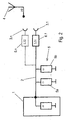
- FIG 2 shows a circuit diagram of a radio frequency apparatus according to a first embodiment of the present invention.
- the RF apparatus comprises a RF transceiver or RF transmitter 1 having an impedance Z0 which is connected to a plurality of antenna connectors 3.1, ..., 3.n via line 2.
- the antenna connectors 3.1, ..., 3.n are adapted to be coupled with external antennas 4 or intern antennas (not shown).
- a parallel resonator circuit 5 also comprising a capacitor 5a (capacitance C1) and an inductor' 5b (inductance L1) is connected to line 2, and the first terminal of the capacitor 5a and of the inductor 5b is connected to line 2, and the second terminal of the capacitor 5a and of the inductor 5b is connected to ground.
- the capacitance C1 of capacitor 5a and the inductance L1 of inductor 5b are chosen to define a parallel resonator circuit serving as a bandpass-filter which theoretically has a high impedance compared to Z0 within the signal frequency bandwidth and a low impedance compared to Z0 outside the signal frequency bandwidth.
- the inventive circuit configuration of Figure 2 comprises one or more additional inductors 6.1, ..., 6.n (having inductances L21, ..., L2n - merely L21 and L22 are shown in Figure 2) connected to line 2 and coupled between the parallel resonator circuit 5 and each of the antenna connectors 3.1, ..., 3.n.
- the passive components i.e. the capacitor C1, the inductor L1, and the inductors L21, ..., L2n, are chosen with respect to their common impedance over the whole frequency range such that:
- the second and third harmonics in the output spectrum of the transmitter (which are the dominant harmonics) can be suppressed in a very effective manner by use of the parasitic reactances, as described above.
- the self resonances of the capacitor 5a and the inductors 6.1, ..., 6.n which are necessary for suppression of the second and third harmonics can be obtained by selection of suitable component technologies for the capacitor 5a and the inductors 6.1, ..., 6.n.
- Tuning to the required overall sum of parasitic capacitances and parasitic inductances of the capacitor 5a and the inductors 6.1, ..., 6.n can be realized by suitable configuration and structure of the electric conductors, for example conductive line 2 and/or the conductive lines of the printed circuit board (PCB) of the RF apparatus and/or terminal connections of said components, to create the desired resonances at the second and third harmonic frequencies.
- PCB printed circuit board
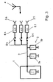
- Figure 3 shows a second embodiment of the invention which is similar to the first embodiment of Figure 2, and the same reference numbers are used to designate components which are identical or similar to those in Figure 2.
- the circuit of the RF apparatus of Figure 3 comprises a plurality of inductors 6.1, ..., 6.n, wherein a first terminal of each inductor is connected to a respective antenna connector 3.1, ..., 3.n, as in Figure 2, and a second terminal of each inductor is connected to a second terminal of a respective switch 8.1, ..., 8.n, wherein the first terminal of each of the switches is connected to line 2.
- each of the antenna connectors 3.1, ..., 3.n is coupled to line 2 via a respective inductor 6.1, ..., 6.n and a respective switch 8.1, ..., 8.n.
- the antenna switches can be realized by simple mechanical or electronic switches as shown in EP 0 718 981 A2 , for example.
- the antenna 4 having impedance Z0 (for example 50 ohms) is coupled via inductor L21 (shown as inductor 6.1) to closed switch 8.1 (switches 8.2, ..., 8.n are open).
- inductor L21 shown as inductor 6.1
- closed switch 8.1 switches 8.2, ..., 8.n are open.
- the discrete components 5a, 5b and 6.1, ..., 6.n are selected with the appropriate parasitic elements in addition to parasitic inductance/capacitance of the printed wiring board as follows:
- the switches 8.1, ..., 8.n may simultaneously perform the function of the inductors 6.1, ..., 6.n, or in other words, the components 6.1, ..., 6.n having inductances L21, ..., L2n may simultaneously perform the function of switches.
- the inductors/components 6.1, ..., 6.n may be selected by mounting a bridge element (not shown) as switch on the printed circuit board, which is often a broadband coupling capacitor.
- the switches 8.1, ..., 8.n can directly be replaced by the inductors as depicted in Figure 2.
- the inductors L21, ..., L2n may for example consist of lumped components for surface mount or bond wires with appropriate dimensions.
- the described discrete inductor/capacitor topology of the present invention takes advantage of parasitic reactances of the components to reduce the number of components.
- the discrete inductors 6.1, ..., 6.n can be omitted as the antenna switches 8.1, ..., 8.n and/or the electric switch contacts thereof are used as the required inductances.
- the space and costs are reduced when the inductors 6.1, ..., 6.n are used as switch contacts, and the remaining components are sufficient to provide a bandpass-filter for the fundamental power, suppression means for the second harmonic, and suppression means for the third harmonic.
- an ISM (Industrial, Scientific and Medical) band transceiver as shown in Figure 2 is operated at a frequency of 2,45 GHz.
- the surface mounted circuit of Figure 2 can be configured for one of two different antenna connectors/terminals 3.1 and 3.2, depending on whether L21 or L22 is inserted.
- the components are a chip capacitor C1 and surface mounted multilayer inductors L1, L21 and L22.
- the parallel resonance of C1 and L1 occurs at appr. 2,45 GHz.
- the series resonance of C1 occurs at appr. 4,9 GHz.
- the parallel resonance of L21 (L22) occurs at appr. 7,35 GHz.
Landscapes
- Transceivers (AREA)
Abstract
Description
- The present invention relates in general to a radio frequency (RF) apparatus, and in particular, to an antenna switching circuit for such a RF apparatus. In one aspect, the RF apparatus of the present invention comprises a RF transceiver circuit incorporating a RF transmitter circuit and a RF receiver circuit for transmitting and receiving RF signals, and an antenna switching circuit for connecting the RF transceiver circuit to one of a plurality of antennas to provide a signal path between the RF transceiver circuit and a selected one of the plurality of antennas. According to another aspect of the invention, the RF apparatus comprises a RF transmitter circuit for transmitting RF signals, and an antenna switching circuit for connecting the RF transmitter circuit to one of a plurality of antennas to provide a signal path between the RF transmitter circuit and a selected one of the plurality of antennas.
- The RF apparatus of the present invention is, for example, a wireless communication apparatus, such as a cell phone or a similar wireless device having at least a built-in internal antenna. When such a wireless communication apparatus is used as a mobile phone, the built-in internal antenna is used for communication. Thus, the antenna switching circuit is adapted to connect the RF transceiver circuit to the internal antenna. However, when the mobile phone is used in a car as a car telephone, an external antenna mounted to the car is used for communication, and the antenna switching circuit is adapted to connect the RF transceiver to the external antenna. Thus, by means of the antenna switching circuit, the signal path to and from the RF transceiver is switched between the internal antenna and the external antenna. It is obvious that instead of an internal antenna and an external antenna, a plurality of different types of antennas can be used, for example, a plurality of internal antennas and/or a plurality of external antennas.
- The antenna switching circuit can be realized by means of a simple mechanical or electronic switch which is operated when the plug of the external antenna cable is inserted in or removed from an external antenna connector. In other words, when the external antenna plug is inserted in the external antenna connector of the RF apparatus, the signal path between the RF transceiver and the internal antenna is disconnected, and a connection between the RF transceiver and the external antenna is established. Such a solution is shown, for example, in
EP 0 718 981 A2 . - In a second example, the RF apparatus is a wireless communication module (w.c.m.) used as a component for electronic devices in order to add wireless communication capability to them. The antenna required for operation of the wireless communication module is selected by design of the electronic device to fit to various parameters, such as space constraints, antenna characteristics and cost. Thus, the RF terminals of a wireless communication module are designed to allow for various antenna terminals without changing the printed wiring board of the wireless communication module.
- A series contact located on the wireless communication module defines the selection of the antenna, as for example:
- 1. a series contact to a socket located on the wireless communication module for a cable connection to an external antenna,
- 2. a series contact to an integrated antenna located on the wireless communication module,
- 3. a series contact to the board where the wireless communication module is mounted on.
- The series contact for antenna selection on the wireless communication module can be for example:
- 1. a component or bondwire inserted on the wireless communication module during assembly of the wireless communication module, or
- 2. a surface mount component inserted on the wireless communication module after insertion of the wireless communication module on of the electronic device, or
- 3. a bondwire serving as interconnection from the wireless communication module to the electronic device.
- Usually, the RF apparatus further comprises a frontend bandpass-filter and/or lowpass-filter for filtering a signal received or transmitted via the antenna switching circuit. The purpose of the bandpass-filter or lowpass-filter is (a), during the receiving operation, to suppress disturbances or interferences of the received signal power outside the signal frequency bandwidth, and (b), during transmission operation, to suppress spectral components outside the signal frequency bandwidth of the transmitted signal. During the transmission operation, harmonics, especially the most dominating second and third harmonics, are critical and not desired because of the emission thereof is restricted by law or regulations.
- One possible solution for suppression of unwanted harmonics is shown in Figure 1 wherein the RF transceiver circuit (or RF transmitter circuit) 1 having an impedance of Z0 is connected to an
antenna connector 3 viaconductive line 2. Theantenna connector 3 is adapted to be coupled with an external orinternal antenna 4. Further, aparallel resonator circuit 5 comprising acapacitor 5a (with capacitance C1) and aninductor 5b (with inductance L1) is connected toline 2. Thecapacitor 5a and theinductor 5b are chosen to define a parallel resonator circuit having a high impedance compared to Z0 within the signal frequency bandwidth (i.e. nearly no load) and a low impedance compared to Z0 outside the signal frequency bandwidth (i.e. nearly short circuit). With this circuit the available suppression of spectral components outside the signal frequency bandwidth withcircuit 5 is limited, and in particular, the suppression of the harmonics of the transmitted signals is often insufficient. - Further, the above mentioned prior art filters, often consisting of discrete inductor/capacitor circuitry or LTCC (Low Temperature Cofired Ceramic) devices, lead to additional costs and require space on the whole RF transceiver circuit board.
- Thus, it is an object of the present invention to alleviate the above mentioned disadvantages and to provide a radio frequency (RF) apparatus, for example for use in wireless communications devices or modules, having an improved antenna switching circuit, and in particular, to provide an antenna switching circuit comprising an improved bandpass-filter for harmonics suppression.
- This object is achieved by a radio frequency apparatus as defined in
claims - The invention will in the following be described in connection with different, non-limiting embodiments shown in the drawings, in which:
- Figure 1 shows a circuit diagram of a prior art radio frequency apparatus having an antenna connector for connecting an external antenna, and a bandpass-filter;
- Figure 2 shows a circuit diagram of a radio frequency apparatus according to a first embodiment of the present invention, having antenna connectors for connecting a plurality of internal/external antennas, and a bandpass-filter; and
- Figure 3 shows a circuit diagram of a radio frequency apparatus according to a second embodiment of the present invention, having antenna connectors for connecting a plurality of internal/external antennas, and a bandpass-filter.
- In the following detailed description, reference is made to the accompanying drawings that form part of it, and in which by way of illustration specific embodiments of the present invention are shown. Embodiments of the present invention provide improvements in a radio frequency apparatus, and in particular, in an antenna switching circuit, which is used in, for example, wireless communication devices such as mobile phones, personal digital assistants (PDA), Bluetooth apparatuses, and wireless communication modules (w.c.m.) used as components for electronic devices in order to add wireless communication capability to them.
- Reference is now made to Figure 1 which shows a schematic circuit diagram of a radio frequency apparatus comprising a RF transceiver or
RF transmitter 1 having an impedance Z0 which is connected to anantenna connector 3 vialine 2. Theantenna connector 3 is adapted to be coupled with anexternal antenna 4. Further, aparallel resonator circuit 5 comprising acapacitor 5a and aninductor 5b is connected toline 2. As shown in Figure 1, the first terminal of thecapacitor 5a and of theinductor 5b is connected toline 2, and the second terminal of thecapacitor 5a and of theinductor 5b is connected to ground. The capacitance C1 ofcapacitor 5a and the inductance L1 ofinductor 5b are chosen to define a resonator circuit having an high impedance compared to Z0 within the signal frequency bandwidth and having a low impedance compared to Z0 outside the signal frequency bandwidth, thus forming a bandpass-filter for the fundamental frequencies. - Figure 2 shows a circuit diagram of a radio frequency apparatus according to a first embodiment of the present invention. As shown in Figure 2, the RF apparatus comprises a RF transceiver or
RF transmitter 1 having an impedance Z0 which is connected to a plurality of antenna connectors 3.1, ..., 3.n vialine 2. The antenna connectors 3.1, ..., 3.n are adapted to be coupled withexternal antennas 4 or intern antennas (not shown). Similar to the prior art embodiment in Figure 1, aparallel resonator circuit 5 also comprising acapacitor 5a (capacitance C1) and aninductor' 5b (inductance L1) is connected toline 2, and the first terminal of thecapacitor 5a and of theinductor 5b is connected toline 2, and the second terminal of thecapacitor 5a and of theinductor 5b is connected to ground. The capacitance C1 ofcapacitor 5a and the inductance L1 ofinductor 5b are chosen to define a parallel resonator circuit serving as a bandpass-filter which theoretically has a high impedance compared to Z0 within the signal frequency bandwidth and a low impedance compared to Z0 outside the signal frequency bandwidth. - In addition to the known radio frequency apparatus circuit configuration of Figure 1, the inventive circuit configuration of Figure 2 comprises one or more additional inductors 6.1, ..., 6.n (having inductances L21, ..., L2n - merely L21 and L22 are shown in Figure 2) connected to
line 2 and coupled between theparallel resonator circuit 5 and each of the antenna connectors 3.1, ..., 3.n. - The passive components, i.e. the capacitor C1, the inductor L1, and the inductors L21, ..., L2n, are chosen with respect to their common impedance over the whole frequency range such that:
- 1. the
capacitor 5a (with its fundamental capacitance C1 and together with its serial parasitic inductance and its serial terminal inductance) forms a series resonator circuit at the second harmonic, for example at 4,8 GHz for a first harmonic at 2,4 GHz in the ISM frequency range, - 2. the inductors 6.1, ..., 6.n (with their fundamental respective inductances L21, ..., L2n and together with their respective parallel parasitic capacitances and their respective parallel terminal capacitances) each form a parallel resonator circuit at the third harmonic, for example at 7,2 GHz for a first harmonic at 2,4 GHz in the ISM frequency range,
- 3. the
inductor 5b (with its fundamental inductance L1 and together with its serial parasitic inductance and its serial terminal inductance) together with thecapacitor 5a (with its fundamental capacitance C1 and together with its serial parasitic inductance and its serial terminal inductance) form a bandpass-filter for the signal frequency bandwidth. - Thus, by means of a suitable selection of the combined impedance of
components 5a and 6.1, ..., 6.n, the second and third harmonics in the output spectrum of the transmitter (which are the dominant harmonics) can be suppressed in a very effective manner by use of the parasitic reactances, as described above. - Further, the self resonances of the
capacitor 5a and the inductors 6.1, ..., 6.n which are necessary for suppression of the second and third harmonics can be obtained by selection of suitable component technologies for thecapacitor 5a and the inductors 6.1, ..., 6.n. Tuning to the required overall sum of parasitic capacitances and parasitic inductances of thecapacitor 5a and the inductors 6.1, ..., 6.n can be realized by suitable configuration and structure of the electric conductors, for exampleconductive line 2 and/or the conductive lines of the printed circuit board (PCB) of the RF apparatus and/or terminal connections of said components, to create the desired resonances at the second and third harmonic frequencies. - Figure 3 shows a second embodiment of the invention which is similar to the first embodiment of Figure 2, and the same reference numbers are used to designate components which are identical or similar to those in Figure 2.
- In addition to the embodiment of Figure 2, the circuit of the RF apparatus of Figure 3 comprises a plurality of inductors 6.1, ..., 6.n, wherein a first terminal of each inductor is connected to a respective antenna connector 3.1, ..., 3.n, as in Figure 2, and a second terminal of each inductor is connected to a second terminal of a respective switch 8.1, ..., 8.n, wherein the first terminal of each of the switches is connected to
line 2. Thus, each of the antenna connectors 3.1, ..., 3.n is coupled toline 2 via a respective inductor 6.1, ..., 6.n and a respective switch 8.1, ..., 8.n. Therefore, it is possible to select one out of a plurality of antennas (internal and/or external antennas) connected to the antenna connectors 3.1, ..., 3.n by setting one of the antenna switches to ON state while all other switches are set to OFF state. As described above, the antenna switches can be realized by simple mechanical or electronic switches as shown inEP 0 718 981 A2 , for example. - As shown in Figure 3, the
antenna 4 having impedance Z0 (for example 50 ohms) is coupled via inductor L21 (shown as inductor 6.1) to closed switch 8.1 (switches 8.2, ..., 8.n are open). As mentioned above, thediscrete components - 1. Bandpass at frequency f0. The capacitance C1 of
capacitor 5a and the inductance L1 ofinductor 5b resonate at the fundamental frequency f0. Supposed that C1 and L1 have high quality factors, the transmission loss at f0 is low. - 2. Suppression of the second harmonic f1. The parasitic inductance in series to capacitance C1 of
capacitor 5a is chosen to resonate with the capacitance C1 at the frequency of the second harmonic f1. Therefore, capacitance C1 is suppressing the second harmonic f1. An additional inductance in series to C1 can be realized by the design of the printed circuit board in order to tuning the series resonance to f1, for example with a ground via at the C1 ground contact. - 3. Suppression of the third harmonic f2. The parasitic capacitance in parallel to inductance L21, ..., L2n resonates with the inductance L21, ..., L2n at f2. Therefore, the third harmonic f2 is suppressed. An additional capacitance in parallel to L21, ..., L2n can be realized by the design of the printed circuit board in order to tune the parallel resonance to f2, for example with a gap in parallel to L21, ..., L2n.
- As an important feature of the present invention, the switches 8.1, ..., 8.n may simultaneously perform the function of the inductors 6.1, ..., 6.n, or in other words, the components 6.1, ..., 6.n having inductances L21, ..., L2n may simultaneously perform the function of switches. Thus, no additional space is required for the inductors/components 6.1, ..., 6.n. This is the case when the antenna connector is selected by mounting a bridge element (not shown) as switch on the printed circuit board, which is often a broadband coupling capacitor. Thus, the switches 8.1, ..., 8.n can directly be replaced by the inductors as depicted in Figure 2. By mounting of one of the inductors L21, ..., L2n on the printed circuit board one of the antenna terminals 3.1, ..., 3.n is activated. The inductors L21, ..., L2n may for example consist of lumped components for surface mount or bond wires with appropriate dimensions.
- Therefore, the described discrete inductor/capacitor topology of the present invention takes advantage of parasitic reactances of the components to reduce the number of components. As described with reference to Figure 3, the discrete inductors 6.1, ..., 6.n can be omitted as the antenna switches 8.1, ..., 8.n and/or the electric switch contacts thereof are used as the required inductances. Thus, the space and costs are reduced when the inductors 6.1, ..., 6.n are used as switch contacts, and the remaining components are sufficient to provide a bandpass-filter for the fundamental power, suppression means for the second harmonic, and suppression means for the third harmonic.
- According to an example, an ISM (Industrial, Scientific and Medical) band transceiver as shown in Figure 2 is operated at a frequency of 2,45 GHz. The surface mounted circuit of Figure 2 can be configured for one of two different antenna connectors/terminals 3.1 and 3.2, depending on whether L21 or L22 is inserted. The components are a chip capacitor C1 and surface mounted multilayer inductors L1, L21 and L22.
-
- C1 =
- 1,2 pF nominal with 0,9 nH total series inductance
- L1 =
- 3,3 nH with 0,15 pF total parallel capacitance
- L21 =
- 3,3 nH with 0,15 pF total parallel capacitance
- L22 =
- 3,3 nH with 0,15 pF total parallel capacitance
- The parallel resonance of C1 and L1 occurs at appr. 2,45 GHz. The series resonance of C1 occurs at appr. 4,9 GHz. The parallel resonance of L21 (L22) occurs at appr. 7,35 GHz.
Claims (28)
- Radio frequency (RF) apparatus comprising:- a radio frequency (RF) transmitter circuit (1) for transmitting RF signals;- an antenna switching circuit for connecting the RF transmitter circuit to one of a plurality of antennas (4) to provide a signal path between the RF transmitter circuit and a selected one of the plurality of antennas (4);- wherein the antenna switching circuit comprising:- a plurality of antenna connectors (3.1, ..., 3.n) coupled to the RF transmitter circuit (1) via a conductive line (2);- a parallel resonator circuit (5) comprising a capacitor (5a) having a capacitance (C1) and an inductor (5b) having an inductance (L1) which is connected to the conductive line (2); and- a plurality of inductors (6.1, ..., 6.n) having inductances (L21, ..., L2n) for coupling each of the plurality of antenna connectors (3.1, ..., 3.n) to the conductive line (2);- wherein the capacitance (C1) of capacitor (5a) and the inductance (L1) of inductor (5b) are chosen to resonate at a fundamental frequency (f0) to form a bandpass-filter at the fundamental frequency (f0);- wherein the parasitic inductances in series to the capacitance (C1) of the capacitor (5a) is chosen to resonate with the capacitance (C1) at the frequency of the second harmonic (f1) of the fundamental frequency (f0); and- wherein the parasitic capacitances in parallel to the inductances (L21, ..., L2n) of the inductors (6.1, ..., 6.n) are chosen to resonate with the inductances (L21, ..., L2n) at the frequency of the third harmonic (f2) of the fundamental frequency (f0).
- Radio frequency (RF) apparatus comprising:- a radio frequency (RF) transceiver circuit (1) incorporating a transmitter circuit and a receiver circuit for transmitting and receiving RF signals;- an antenna switching circuit for connecting the RF transceiver circuit to one of a plurality of antennas (4) to provide a signal path between the RF transceiver circuit and a selected one of the plurality of antennas (4);- wherein the antenna switching circuit comprising:- a plurality of antenna connectors (3.1, ..., 3.n) coupled to the RF transmitter circuit (1) via a conductive line (2);- a parallel resonator circuit (5) comprising a capacitor (5a) having a capacitance (C1) and an inductor (5b) having an inductance (L1) which is connected to the conductive line (2); and- a plurality of inductors (6.1, ..., 6.n) having inductances (L21, ..., L2n) for coupling each of the plurality of antenna connectors (3.1, ..., 3.n) to the conductive line (2);- wherein the capacitance (C1) of capacitor (5a) and the inductance (L1) of inductor (5b) are chosen to resonate at a fundamental frequency (f0) to form a bandpass-filter at the fundamental frequency (f0);- wherein the parasitic inductances in series to the capacitance (C1) of the capacitor (5a) is chosen to resonate with the capacitance (C1) at the frequency of the second harmonic (f1) of the fundamental frequency (f0) ; and- wherein the parasitic capacitances in parallel to the inductances (L21, ..., L2n) of the inductors (6.1, ..., 6.n) are chosen to resonate with the inductances (L21, ..., L2n) at the frequency of the third harmonic (f2) of the fundamental frequency (f0).
- Radio frequency (RF) apparatus according to claim 1 or claim 2, wherein the parasitic inductance in series to the capacitance (C1) of the capacitor (5a) can be realized fully or partly by the design of the printed circuit board of the radio frequency (RF) apparatus in order to tune the series resonance to the frequency of the second harmonic (f1).
- Radio frequency (RF) apparatus according to any of the preceding claims, wherein the parasitic capacitances in parallel to the inductances (L21, ..., L2n) of the inductors (6.1, ..., 6.n) can be realized fully or partly by the design of the printed circuit board of the radio frequency (RF) apparatus in order to tune the parallel resonance to the frequency of the third harmonic (f2).
- Radio frequency (RF) apparatus according to any of the preceding claims, wherein a first terminal of the capacitor (5a) and a first terminal of the inductor (5b) are connected to conductive line (2), and the second terminal of the capacitor (5a) and the second terminal of the inductor (5b) are connected to ground.
- Radio frequency (RF) apparatus according to any of the preceding claims, wherein the capacitance (C1) of capacitor (5a) and the inductance (L1) of inductor (5b) are chosen to define a parallel resonator circuit serving as a bandpass-filter which has a high impedance compared to Z0 within the signal frequency bandwidth (f0) and a low impedance compared to Z0 outside the signal frequency bandwidth (f0).
- Radio frequency (RF) apparatus according to any of the preceding claims, wherein the antenna connectors (3.1, ..., 3.n) are adapted to be coupled with external antennas (4) or internal antennas.
- Radio frequency (RF) apparatus according to any of the preceding claims, wherein tuning of the required overall parasitic capacitances and inductances of the capacitor (5a) and the inductors (6.1, ..., 6.n) is realized by suitable configuration and structure of electric conductors and/or conductive line (2) and/or the conductive lines of the printed circuit board (PCB) of the RF apparatus and/or terminal connections of said components.
- Radio frequency (RF) apparatus according to any of the preceding claims, wherein a first terminal of each of the plurality of inductors (6.1, ..., 6.n) is connected to a respective one of the plurality of antenna connectors (3.1, ..., 3.n), and a second terminal of each of the plurality of inductors is connected to a second terminal of a respective switch (8.1, ..., 8.n), wherein the first terminal of each of the switches is connected to conductive line (2).
- Radio frequency (RF) apparatus according to claim 9, wherein each of the antenna connectors (3.1, ..., 3.n) is coupled to conductive line (2) via a respective inductor (6.1, ..., 6.n) and a respective switch (8.1, ..., 8.n) to select one of the plurality of antennas connected to the antenna connectors (3.1, ..., 3.n) by setting one of the antenna switches to the ON state.
- Radio frequency (RF) apparatus according to any of claims 9 and 10, wherein the antenna switches are realized by simple mechanical or electronic switches.
- Radio frequency (RF) apparatus according to any of the preceding claims, wherein the RF apparatus is a wireless communication apparatus, such as a cell phone or a similar wireless device.
- Radio frequency (RF) apparatus according to any of the preceding claims, wherein the RF apparatus is a module intended for adding wireless communication capability to electronic devices.
- Radio frequency (RF) apparatus according to any of the preceding claims, wherein the switches (8.1, ..., 8.n) and/or the inductors (6.1, ..., 6.n) of the RF apparatus are a wire or a via interconnection between modules and/or printed circuit boards.
- Antenna switching circuit for a radio frequency (RF) apparatus having a radio frequency (RF) transceiver circuit (1) for connecting the RF transceiver circuit to one of a plurality of antennas (4) to provide a.signal path between the RF transceiver circuit and a selected one of the plurality of antennas (4);
wherein the RF transceiver circuit (1) having a RF transmitter circuit and a RF receiver circuit for transmitting and receiving RF signals;
wherein the antenna switching circuit comprising:- a plurality of antenna connectors (3.1, ..., 3.n) coupled to the RF transceiver circuit (1) via a conductive line (2);- a parallel resonator circuit (5) comprising a capacitor (5a) having a capacitance (C1) and an inductor (5b) having an inductance (L1) which is connected to the conductive line (2); and- a plurality of inductors (6.1, ..., 6.n) having inductances (L21, ..., L2n) for coupling each of the plurality of antenna connectors (3.1, ..., 3.n) to the conductive line (2);wherein the capacitance (C1) of capacitor (5a) and the inductance (L1) of inductor (5b) are chosen to resonate at a fundamental frequency (f0) to form a bandpass-filter at the fundamental frequency (f0);
wherein the parasitic inductance in series to the capacitance (C1) of the capacitor (5a) is chosen to resonate with the capacitance (C1) at the frequency of the second harmonic (f1) of the fundamental frequency (f0) ; and
wherein the parasitic capacitances in parallel to the inductances (L21, ..., L2n) of the inductors (6.1, ..., 6.n) are chosen to resonate with the inductances (L21, ..., L2n) at the frequency of the third harmonic (f2) of the fundamental frequency (f0). - Antenna switching circuit for a radio frequency (RF) apparatus having a radio frequency (RF) transmitter circuit (1) for connecting the RF transmitter circuit to one of a plurality of antennas (4) to provide a signal path between the RF transmitter circuit and a selected one of the plurality of antennas (4);
wherein the RF transmitter circuit (1) is adapted for transmitting RF signals;
wherein the antenna switching circuit comprising:- a plurality of antenna connectors (3.1, ..., 3.n) coupled to the RF transmitter circuit (1) via a conductive line (2);- a parallel resonator circuit (5) comprising a capacitor (5a) having a capacitance (C1) and an inductor (5b) having an inductance (L1) which is connected to the conductive line (2); and- a plurality of inductors (6.1, ..., 6.n) having inductances (L21, ..., L2n) for coupling each of the plurality of antenna connectors (3.1, ..., 3.n) to the conductive line (2);wherein the capacitance (C1) of capacitor (5a) and the inductance (L1) of inductor (5b) are chosen to resonate at a fundamental frequency (f0) to form a bandpass-filter at the fundamental frequency (f0);
wherein the parasitic inductance in series to the capacitance (C1) of the capacitor (5a) is chosen to resonate with the capacitance (C1) at the frequency of the second harmonic (f1) of the fundamental frequency (f0) ; and
wherein the parasitic capacitances in parallel to the inductances (L21, ..., L2n) of the inductors (6.1, ..., 6.n) are chosen to resonate with the inductances (L21, ..., L2n) at the frequency of the third harmonic (f2) of the fundamental frequency (f0). - Antenna switching circuit according to claim 15 or claim 16, wherein the parasitic inductance in series to the capacitance (C1) of the capacitor (5a) is fully or partly realized by the design of the printed circuit board of the radio frequency (RF) apparatus in order to tune the series resonance to the frequency of the second harmonic (f1).
- Antenna switching circuit according to any of claims 15 to 16, wherein the parasitic capacitances in parallel to the inductances (L21, ..., L2n) of the inductors (6.1, ..., 6.n) is fully or partly realized by the design of the printed circuit board of the radio frequency (RF) apparatus in order to tune the parallel resonance to the frequency of the third harmonic (f2).
- Antenna switching circuit according to any of claims 15 to 18, wherein a first terminal of the capacitor (5a) and a first terminal of the inductor (5b) are connected to conductive line (2), and the second terminal of the capacitor (5a) and the second terminal of the inductor (5b) are connected to ground.
- Antenna switching circuit according to any the claims 15 to 19, wherein the capacitance (C1) of capacitor (5a) and the inductance (L1) of inductor (5b) are chosen to define a parallel resonator circuit serving as a bandpass-filter which has a high impedance compared to Z0 within the signal frequency bandwidth (f0) and a low impedance compared to Z0 outside the signal frequency bandwidth (f0).
- Antenna switching circuit according to any of claims 15 to 20, wherein the antenna connectors (3.1, ..., 3.n) are adapted to be coupled with external antennas (4) or internal antennas.
- Antenna switching circuit according to any of claims 15 to 21, wherein tuning of the parasitic capacitances and inductances of the capacitor (5a) and the inductors (6.1, ..., 6.n) is realized by suitable configuration and structure of electric conductors and/or conductive line (2) and/or the conductive lines of the printed circuit board (PCB) of the RF apparatus and/or terminal connections of said components.
- Antenna switching circuit according to any of claims 15 to 22, wherein a first terminal of each of the plurality of inductors (6.1, ..., 6.n) is connected to a respective one of the plurality of antenna connectors (3.1, ..., 3.n), and a second terminal of each of the plurality of inductors is connected to a second terminal of a respective switch (8.1, ..., 8.n), wherein the first terminal of each of the switches is connected to conductive line (2).
- Antenna switching circuit according to claim 23, wherein each of the antenna connectors (3.1, ..., 3.n) is coupled to conductive line (2) via a respective inductor (6.1, ..., 6.n) and a respective switch (8.1, ..., 8.n) to select one of the plurality of antennas connected to the antenna connectors (3.1, ..., 3.n) by switching one of the antenna switches to ON state.
- Antenna switching circuit according to any of claims 23 and 24, wherein the antenna switches are realized by simple mechanical or electronic switches.
- Antenna switching circuit according to any of claims 15 to 25, wherein the RF apparatus is a wireless communication apparatus, such as a cell phone or a similar wireless device.
- Antenna switching circuit according to any of claims 15 to 26, wherein the RF apparatus is a module intended for adding wireless communication capability to electronic devices.
- Antenna switching circuit according to any of claims 15 to 27, wherein the switches (8.1, ..., 8.n) and/or the inductors (6.1, ..., 6.n) of the antenna switching circuit are a wire or a via interconnection between modules and/or printed circuit boards.
Priority Applications (1)
| Application Number | Priority Date | Filing Date | Title |
|---|---|---|---|
| EP20060022820 EP1919027B1 (en) | 2006-11-02 | 2006-11-02 | Antenna switching circuit with band pass filter and harmonics suppression |
Applications Claiming Priority (1)
| Application Number | Priority Date | Filing Date | Title |
|---|---|---|---|
| EP20060022820 EP1919027B1 (en) | 2006-11-02 | 2006-11-02 | Antenna switching circuit with band pass filter and harmonics suppression |
Publications (2)
| Publication Number | Publication Date |
|---|---|
| EP1919027A1 true EP1919027A1 (en) | 2008-05-07 |
| EP1919027B1 EP1919027B1 (en) | 2012-04-04 |
Family
ID=37882347
Family Applications (1)
| Application Number | Title | Priority Date | Filing Date |
|---|---|---|---|
| EP20060022820 Not-in-force EP1919027B1 (en) | 2006-11-02 | 2006-11-02 | Antenna switching circuit with band pass filter and harmonics suppression |
Country Status (1)
| Country | Link |
|---|---|
| EP (1) | EP1919027B1 (en) |
Cited By (6)
| Publication number | Priority date | Publication date | Assignee | Title |
|---|---|---|---|---|
| US20140246916A1 (en) * | 2013-03-01 | 2014-09-04 | Qualcomm Incorporated | Active and adaptive field cancellation for wireless power systems |
| KR101479962B1 (en) * | 2013-04-26 | 2015-01-08 | 주식회사 아이.티.에프 | Variable Bandpass Filter Device and Mobile Communication Repeater |
| CN112204814A (en) * | 2018-06-29 | 2021-01-08 | 谷歌有限责任公司 | Wearable device with antenna plated on high permittivity housing material |
| CN113471697A (en) * | 2020-03-31 | 2021-10-01 | 昇佳电子股份有限公司 | Transmission architecture of antenna and proximity sensing circuit |
| CN115117623A (en) * | 2022-07-29 | 2022-09-27 | 歌尔科技有限公司 | An open-slot antenna pair and antenna terminal |
| TWI912680B (en) * | 2023-12-28 | 2026-01-21 | 啓碁科技股份有限公司 | Sensing module and electronic device |
Families Citing this family (1)
| Publication number | Priority date | Publication date | Assignee | Title |
|---|---|---|---|---|
| CN108183331B (en) * | 2017-12-14 | 2020-12-01 | Oppo广东移动通信有限公司 | Antenna tuning circuit, antenna device and mobile terminal |
Citations (4)
| Publication number | Priority date | Publication date | Assignee | Title |
|---|---|---|---|---|
| GB2293277A (en) | 1994-09-16 | 1996-03-20 | Motorola Inc | Antenna structure and a radio communication device incorporating same |
| EP0932216A1 (en) | 1998-01-22 | 1999-07-28 | Murata Manufacturing Co., Ltd. | High-frequency composite unit |
| US20020044092A1 (en) * | 2000-08-24 | 2002-04-18 | Yuichi Kushihi | Antenna device and radio equipment having the same |
| US7053845B1 (en) | 2003-01-10 | 2006-05-30 | Comant Industries, Inc. | Combination aircraft antenna assemblies |
-
2006
- 2006-11-02 EP EP20060022820 patent/EP1919027B1/en not_active Not-in-force
Patent Citations (4)
| Publication number | Priority date | Publication date | Assignee | Title |
|---|---|---|---|---|
| GB2293277A (en) | 1994-09-16 | 1996-03-20 | Motorola Inc | Antenna structure and a radio communication device incorporating same |
| EP0932216A1 (en) | 1998-01-22 | 1999-07-28 | Murata Manufacturing Co., Ltd. | High-frequency composite unit |
| US20020044092A1 (en) * | 2000-08-24 | 2002-04-18 | Yuichi Kushihi | Antenna device and radio equipment having the same |
| US7053845B1 (en) | 2003-01-10 | 2006-05-30 | Comant Industries, Inc. | Combination aircraft antenna assemblies |
Cited By (8)
| Publication number | Priority date | Publication date | Assignee | Title |
|---|---|---|---|---|
| US20140246916A1 (en) * | 2013-03-01 | 2014-09-04 | Qualcomm Incorporated | Active and adaptive field cancellation for wireless power systems |
| US9819228B2 (en) * | 2013-03-01 | 2017-11-14 | Qualcomm Incorporated | Active and adaptive field cancellation for wireless power systems |
| KR101479962B1 (en) * | 2013-04-26 | 2015-01-08 | 주식회사 아이.티.에프 | Variable Bandpass Filter Device and Mobile Communication Repeater |
| CN112204814A (en) * | 2018-06-29 | 2021-01-08 | 谷歌有限责任公司 | Wearable device with antenna plated on high permittivity housing material |
| CN113471697A (en) * | 2020-03-31 | 2021-10-01 | 昇佳电子股份有限公司 | Transmission architecture of antenna and proximity sensing circuit |
| CN113471697B (en) * | 2020-03-31 | 2023-12-15 | 昇佳电子股份有限公司 | Transmission architecture of antenna and proximity sensing circuit |
| CN115117623A (en) * | 2022-07-29 | 2022-09-27 | 歌尔科技有限公司 | An open-slot antenna pair and antenna terminal |
| TWI912680B (en) * | 2023-12-28 | 2026-01-21 | 啓碁科技股份有限公司 | Sensing module and electronic device |
Also Published As
| Publication number | Publication date |
|---|---|
| EP1919027B1 (en) | 2012-04-04 |
Similar Documents
| Publication | Publication Date | Title |
|---|---|---|
| EP1362388B1 (en) | Patch antenna with switchable reactive components for multiple frequency use in mobile communications | |
| JP5262413B2 (en) | Multiband duplexer module | |
| JP4531399B2 (en) | Transmit and / or receive module | |
| US8681062B2 (en) | Antenna, wireless communication apparatus and method of configuring antenna | |
| EP1261143A1 (en) | Transceiver front end module | |
| US10263315B2 (en) | Directional coupler and communication module | |
| WO2005083835A2 (en) | Antenna | |
| US20050037800A1 (en) | Front end module for mobile telecommunication system | |
| US6693593B1 (en) | High frequency circuit with a connection for a printed antenna | |
| KR100512794B1 (en) | Filter component and communication apparatus | |
| EP1919027B1 (en) | Antenna switching circuit with band pass filter and harmonics suppression | |
| EP1430612B1 (en) | Rf signal switch for a wireless communication device | |
| US20060058000A1 (en) | Integrated radio frequency module | |
| KR101126676B1 (en) | Filter for multi-band antenna switching module | |
| US10868518B2 (en) | Elastic wave device | |
| KR100737073B1 (en) | Intergrated circuit board structure of Radio Frequency communication module | |
| CN118285024A (en) | Antenna module | |
| KR20070110957A (en) | Front end module | |
| KR20090000380A (en) | Front end module and its manufacturing method | |
| CN223261537U (en) | Radio frequency front-end module and radio frequency front-end circuit | |
| US12389530B2 (en) | Filter module, filter element, and electronic device | |
| KR20050053829A (en) | Dual band front end module | |
| JP2005136888A (en) | High frequency demultiplexing circuit, high frequency component, high frequency module and wireless communication device equipped with the same | |
| KR100550539B1 (en) | Surface acoustic wave duplexer and manufacturing method thereof | |
| US7812690B2 (en) | Compact power-agile filter, particularly for radiocommunication system amplification module |
Legal Events
| Date | Code | Title | Description |
|---|---|---|---|
| PUAI | Public reference made under article 153(3) epc to a published international application that has entered the european phase |
Free format text: ORIGINAL CODE: 0009012 |
|
| AK | Designated contracting states |
Kind code of ref document: A1 Designated state(s): AT BE BG CH CY CZ DE DK EE ES FI FR GB GR HU IE IS IT LI LT LU LV MC NL PL PT RO SE SI SK TR |
|
| AX | Request for extension of the european patent |
Extension state: AL BA HR MK RS |
|
| 17P | Request for examination filed |
Effective date: 20080804 |
|
| 17Q | First examination report despatched |
Effective date: 20080904 |
|
| RAP1 | Party data changed (applicant data changed or rights of an application transferred) |
Owner name: PANASONIC CORPORATION |
|
| AKX | Designation fees paid |
Designated state(s): DE FR GB |
|
| GRAP | Despatch of communication of intention to grant a patent |
Free format text: ORIGINAL CODE: EPIDOSNIGR1 |
|
| GRAS | Grant fee paid |
Free format text: ORIGINAL CODE: EPIDOSNIGR3 |
|
| GRAA | (expected) grant |
Free format text: ORIGINAL CODE: 0009210 |
|
| AK | Designated contracting states |
Kind code of ref document: B1 Designated state(s): DE FR GB |
|
| REG | Reference to a national code |
Ref country code: GB Ref legal event code: FG4D |
|
| REG | Reference to a national code |
Ref country code: DE Ref legal event code: R096 Ref document number: 602006028574 Country of ref document: DE Effective date: 20120531 |
|
| PLBE | No opposition filed within time limit |
Free format text: ORIGINAL CODE: 0009261 |
|
| STAA | Information on the status of an ep patent application or granted ep patent |
Free format text: STATUS: NO OPPOSITION FILED WITHIN TIME LIMIT |
|
| 26N | No opposition filed |
Effective date: 20130107 |
|
| REG | Reference to a national code |
Ref country code: DE Ref legal event code: R097 Ref document number: 602006028574 Country of ref document: DE Effective date: 20130107 |
|
| PGFP | Annual fee paid to national office [announced via postgrant information from national office to epo] |
Ref country code: DE Payment date: 20141119 Year of fee payment: 9 Ref country code: FR Payment date: 20141119 Year of fee payment: 9 Ref country code: GB Payment date: 20141119 Year of fee payment: 9 |
|
| REG | Reference to a national code |
Ref country code: DE Ref legal event code: R119 Ref document number: 602006028574 Country of ref document: DE |
|
| GBPC | Gb: european patent ceased through non-payment of renewal fee |
Effective date: 20151102 |
|
| REG | Reference to a national code |
Ref country code: FR Ref legal event code: ST Effective date: 20160729 |
|
| PG25 | Lapsed in a contracting state [announced via postgrant information from national office to epo] |
Ref country code: DE Free format text: LAPSE BECAUSE OF NON-PAYMENT OF DUE FEES Effective date: 20160601 Ref country code: GB Free format text: LAPSE BECAUSE OF NON-PAYMENT OF DUE FEES Effective date: 20151102 |
|
| PG25 | Lapsed in a contracting state [announced via postgrant information from national office to epo] |
Ref country code: FR Free format text: LAPSE BECAUSE OF NON-PAYMENT OF DUE FEES Effective date: 20151130 |