EP1918747A1 - Small-form-factor fiber optic transceiver module having built-in test capability and method - Google Patents
Small-form-factor fiber optic transceiver module having built-in test capability and method Download PDFInfo
- Publication number
- EP1918747A1 EP1918747A1 EP07254187A EP07254187A EP1918747A1 EP 1918747 A1 EP1918747 A1 EP 1918747A1 EP 07254187 A EP07254187 A EP 07254187A EP 07254187 A EP07254187 A EP 07254187A EP 1918747 A1 EP1918747 A1 EP 1918747A1
- Authority
- EP
- European Patent Office
- Prior art keywords
- optical
- optical fiber
- fiber
- transceiver module
- fiber optic
- Prior art date
- Legal status (The legal status is an assumption and is not a legal conclusion. Google has not performed a legal analysis and makes no representation as to the accuracy of the status listed.)
- Granted
Links
Images
Classifications
-
- G—PHYSICS
- G02—OPTICS
- G02B—OPTICAL ELEMENTS, SYSTEMS OR APPARATUS
- G02B6/00—Light guides; Structural details of arrangements comprising light guides and other optical elements, e.g. couplings
- G02B6/24—Coupling light guides
- G02B6/42—Coupling light guides with opto-electronic elements
- G02B6/4201—Packages, e.g. shape, construction, internal or external details
- G02B6/4204—Packages, e.g. shape, construction, internal or external details the coupling comprising intermediate optical elements, e.g. lenses, holograms
- G02B6/4214—Packages, e.g. shape, construction, internal or external details the coupling comprising intermediate optical elements, e.g. lenses, holograms the intermediate optical element having redirecting reflective means, e.g. mirrors, prisms for deflecting the radiation from horizontal to down- or upward direction toward a device
-
- G—PHYSICS
- G01—MEASURING; TESTING
- G01M—TESTING STATIC OR DYNAMIC BALANCE OF MACHINES OR STRUCTURES; TESTING OF STRUCTURES OR APPARATUS, NOT OTHERWISE PROVIDED FOR
- G01M11/00—Testing of optical apparatus; Testing structures by optical methods not otherwise provided for
- G01M11/30—Testing of optical devices, constituted by fibre optics or optical waveguides
- G01M11/31—Testing of optical devices, constituted by fibre optics or optical waveguides with a light emitter and a light receiver being disposed at the same side of a fibre or waveguide end-face, e.g. reflectometers
- G01M11/3109—Reflectometers detecting the back-scattered light in the time-domain, e.g. OTDR
- G01M11/3136—Reflectometers detecting the back-scattered light in the time-domain, e.g. OTDR for testing of multiple fibers
-
- G—PHYSICS
- G02—OPTICS
- G02B—OPTICAL ELEMENTS, SYSTEMS OR APPARATUS
- G02B6/00—Light guides; Structural details of arrangements comprising light guides and other optical elements, e.g. couplings
- G02B6/24—Coupling light guides
- G02B6/42—Coupling light guides with opto-electronic elements
- G02B6/4201—Packages, e.g. shape, construction, internal or external details
- G02B6/4204—Packages, e.g. shape, construction, internal or external details the coupling comprising intermediate optical elements, e.g. lenses, holograms
- G02B6/421—Packages, e.g. shape, construction, internal or external details the coupling comprising intermediate optical elements, e.g. lenses, holograms the intermediate optical component consisting of a short length of fibre, e.g. fibre stub
-
- G—PHYSICS
- G02—OPTICS
- G02B—OPTICAL ELEMENTS, SYSTEMS OR APPARATUS
- G02B6/00—Light guides; Structural details of arrangements comprising light guides and other optical elements, e.g. couplings
- G02B6/24—Coupling light guides
- G02B6/42—Coupling light guides with opto-electronic elements
- G02B6/4201—Packages, e.g. shape, construction, internal or external details
- G02B6/4246—Bidirectionally operating package structures
-
- H—ELECTRICITY
- H10—SEMICONDUCTOR DEVICES; ELECTRIC SOLID-STATE DEVICES NOT OTHERWISE PROVIDED FOR
- H10W—GENERIC PACKAGES, INTERCONNECTIONS, CONNECTORS OR OTHER CONSTRUCTIONAL DETAILS OF DEVICES COVERED BY CLASS H10
- H10W90/00—Package configurations
- H10W90/701—Package configurations characterised by the relative positions of pads or connectors relative to package parts
- H10W90/751—Package configurations characterised by the relative positions of pads or connectors relative to package parts of bond wires
- H10W90/753—Package configurations characterised by the relative positions of pads or connectors relative to package parts of bond wires between laterally-adjacent chips
Definitions
- the present invention relates generally to fiber optic transceiver modules, and more particularly, to small-form-factor (SFF) fiber optic transceiver modules having built-in test capability.
- SFF small-form-factor
- Fiber optic connections rather than metallic wiring, for communications, weaponry, and other systems.
- Optical fiber connections provide faster communication speed, increased bandwidths, EMI isolation and light weight.
- optical fiber can be more fragile than metallic wiring and can be damaged during installation, during the rigors of flight testing or during flight operation.
- Damage to optical fiber can be difficult to distinguish from faults occurring in other components of the aircraft systems. Even when it is known that the damage exists, it can be difficult to identify the precise location of the damage. These difficulties can increase the maintenance costs and reduce the operating efficiency of the aircraft.
- BIT capability may be incorporated directly into the fiber optic transceiver module that is otherwise responsible for transmitting and receiving signals via the optical fibers in the cable plant of an airplane.
- Transceivers with BIT capability may also be employed in local area networks in the telecommunication industry where fibers are buried underground or installed inside tight building space.
- BIT capability in a transceiver module the optical fiber can be routinely tested for any discontinuities in the optical fiber that are indicative of damage. For example, the optical fiber can be tested for breaks and contamination every time the system is started.
- a transceiver having BIT capabilities identifies the precise location of the fiber damage, thereby avoiding costly maintenance and repairs where the entire fiber network needs to be checked with bulky and expensive equipment operated by expensive, highly skilled personnel.
- SFF small-form-factor
- MSA multi-source agreement
- Certain military and aerospace platforms are installed with SFF transceivers but without BIT capabilities.
- SFF transceivers require expensive maintenance and repair costs when fiber damage occurs in the cable plant. It is therefore highly desirable to have a fiber optic transceiver module that meets SFF requirements and also has built-in test capability.
- a fiber optic transceiver module having built-in test capability is packaged in a housing to meet small-form-factor (SFF) requirements.
- a first optical fiber is provided having an angled end that defines an acute angle relative to a longitudinal axis of the first optical fiber.
- a second optical fiber also has an angled end that defines an acute angle relative to the longitudinal axis of the second optical fiber.
- the first optical fiber and the second optical fiber are aligned with one another.
- An optical source emits an optical signal propagated along the first optical fiber in which a portion of the optical signal is received at the second optical fiber and is propagated along the second optical fiber.
- An optical detector receives a return optical signal transmitted through the angled end of the second optical fiber in response to reflection from a discontinuity in the optical path of the second optical fiber.
- a fiber optic transceiver module having built-in test capabilities (BIT), and associated method for detecting discontinuities (such as breaks) in the optical fiber that are connected to the transceiver module are provided.
- An optical source emits an optical signal that is reflected by an angled end of the optical fiber.
- a portion of the optical signal is received at a second optical fiber and is propagated along the second optical fiber.
- the second optical fiber has an angled end that is aligned with the angled end of the first optical fiber. If the portion of optical signal propagating along the second optical fiber encounters a discontinuity in the optical path of the second optical fiber, at least a portion of this optical signal is reflected along the second optical fiber back towards the angled end.
- the reflected return optical signal When the reflected return optical signal reaches the angled end of the second optical fiber, some portion of the reflected return signal is reflected and passed through the angled end and is received by an optical detector. By analyzing the time that has elapsed from the emission of the optical signal by the optical source to the reflected return optical signal pulse detected by the optical detector, the existence and location of the discontinuity may be determined.
- the use of angled ends in the optical fibers enables the fiber optic transceiver module to achieve BIT functionality while meeting SFF requirements without using bulky optical components to split the optical signals, such as prisms and lenses.
- a SFF fiber optic transceiver module having BIT capabilities employs a pair of fiber optic cables having their respective ends held and aligned, in a groove of a silicon coupler.
- a first optical fiber has an angled end that defines an acute angle relative to a longitudinal axis of the first optical fiber.
- the second optical fiber also has an angled end that defines an acute angle relative to a longitudinal axis of the second optical fiber.
- the angled ends of the first and second optical fibers are matingly aligned with one another.
- the acute angle for both the angled ends of the first and second optical fibers may, for example, both be between 40 degrees and 60 degrees. In one example, the acute angle for both the first and the second optical fibers is 49 degrees.
- An optical source emits an optical signal that is propagated along the first optical fiber.
- the optical signal is split at the angled end of the first optical fiber such that a portion of the optical signal is received at the second optical fiber and is propagated along the second optical fiber.
- An optical detector receives a return optical signal through the angled end of the second optical fiber in response to reflection from a discontinuity in the second optical fiber and the fiber segments that are connected to it.
- fiber optic transceiver module 10 is shown.
- fiber optic transceiver module 10 is a SFF transceiver module such that SFF requirements are met in addition to having BIT functionality.
- optical source 12 such as a vertical cavity surface emitting laser (VCSEL)
- VCSEL vertical cavity surface emitting laser
- PWB printed wiring board
- ODR optical time domain reflectometer
- IC integrated circuit
- processor 26 and post amplifier circuit 28.
- the components of fiber optic transceiver module 10 are packaged such that SFF requirements are met.
- SFF requirements are 2 x 5, 6 or 7 dual-in-line package (DIP), 0.55" x 2.5" x 0.35" package dimensions, 3.3 volt power supply, as well as other technical requirements.
- VCSEL 12 is held on submount 30 and is controlled by driver circuit 22, which may be an ASIC.
- the optical source 12 may be controlled or activated in many other manners.
- Alternative optical sources, such as edge emitting laser diode, may also be employed.
- First optical fiber 18 is generally a short fiber used to couple optical signal 16 from VCSEL 12.
- First optical fiber 18 is positioned to receive optical signal 16 and transmit the optical signal to second optical fiber 32.
- Second optical fiber 32 is generally a long fiber (e.g.
- Second optical fiber 32 extends outside of the housing 14 and may be used to carry a portion of optical signal 34 to another transceiver (not shown) in the fiber cable plant of an airplane.
- first optical fiber 18 has angled end 36 that defines an acute angle 38 relative to a longitudinal axis of the first optical fiber.
- second optical fiber 32 has angled end 40 that defines an acute angle 42 relative to a longitudinal axis of the second optical fiber.
- the angled ends 36, 40 may be disposed at an angle of between approximately 40 degrees and 60 degrees relative to the longitudinal axis of their corresponding optical fiber.
- the angled end 36 of first optical fiber 18 is aligned to be substantially parallel with the angled end 40 of second optical fiber 32.
- the acute angle 38 for the first optical fiber 18 and the acute angle 42 for the second optical fiber 32 may be the same.
- the acute angle 38 for the angled end 36 of first optical fiber 18 and the acute angle 42 for the angled end 40 of the second optical fiber 32 may both be approximately 49 degrees.
- the acute angle 38 of the angled end 36 of the first optical fiber 18 is selected to cause a predefined portion of optical signal 16 emitted from VCSEL 12 to be received at and propagated along second optical fiber 32.
- Angled end 36 of first optical fiber 18 splits the optical signal 16 such that approximately fifty percent of the optical signal coupled from VCSEL 12 passes from first optical fiber 18 is received at second optical fiber 32, when an angle of approximately 49 degrees is employed.
- a portion of optical signal 34 is then carried along the second optical fiber 32, which may be connected externally to another transceiver (not shown) through the fiber optic cable plant.
- Second optical fiber 32 may exit the housing, for example, through a hermetically sealed feed-through, or by connectorization.
- a reflected return optical signal 46 returns to the angled end 40 of the second optical fiber 32.
- Optical detector 52 receives the return optical signal 54 reflected by the angled end 40 of the second optical fiber 32, this reflected signal is from a discontinuity in the optical path of the second optical fiber 32.
- approximately fifty percent of the return optical signal 46 is reflected from the angled end 40 of the second optical fiber 32 to the optical detector 52.
- coupler 56 embeds and aligns the two optical fibers 18, 32.
- Coupler 56 may be formed of a silicon material.
- groove 58 Formed within coupler 56 is groove 58 that may, for instance be V-shaped to hold and align the ends 36, 40 of the first and second optical fibers 18, 32.
- the optical fibers for instance, may be 100/140 micron multi-mode (MM) optical fibers embedded in V-shaped groove 58 of silicon coupler 56.
- MM micron multi-mode
- other types of optical fibers may selectively be employed.
- the completed structure may be called a 3 dB silicon V-groove coupler.
- a 3 dB coupler is a miniaturized 3 dB coupler which allows the BIT transceiver module to be fabricated under the small dimensional requirements of a SFF transceiver.
- the silicon coupler 56 has a short fiber section holding first optical fiber 18 coupling directly to VCSEL 12 and a long section holding angled end 40 of the long second optical fiber 32 that forms the pigtail of the transceiver.
- the pair of optical fibers 18 and 32 have their respective angled ends 36, 40 aligned in mating relationship forming an angled interface within the V-shaped groove 58 of the coupler 56.
- the coating of the shorter first optical fiber 18 may be removed, with the first optical fiber embedded in the V-shaped groove 58.
- the coating of the second optical fiber 32 may also be stripped from the area proximate the angled end 40.
- the V-shaped groove 58 of the coupler 56 may include a region having a wider opening for embedding the coated section of the longer second optical fiber 32.
- An epoxy may be used to hold the optical fibers 18, 32 embedded in the V-shaped groove 58.
- a portion of the second optical fiber 32 may extend outward from the end of V-shaped groove 58 to the outside of housing 14 to form the fiber pigtail of the BIT transceiver.
- a reflected return optical signal 46 returns to the angled end 40 of the second optical fiber.
- a portion of the return optical signal 46 is reflected on to the optical detector 52. For instance, in the example where an angled end 40 of approximately 49 degrees is employed for second optical fiber 32, approximately fifty percent of the return optical signal 46 is reflected from the angled end 40 of second optical fiber to optical detector 52.
- Optical detector 52 may comprise a photodetector, such as a p-type-intrinsic-n-type (PIN) photodiode, an avalanche photodiode, or any other suitable photo detector known to those skilled in the art.
- PIN p-type-intrinsic-n-type
- IC transimpedance amplifier
- optical signal 54 is a portion of the return optical signal 46 reflected by angled end 40 of second optical fiber 32 onto the optical detector 52 which has its optical axis 63 positioned at approximately 90 degrees to the silicon V-groove 58 surface (see Fig.
- Optical detector 52 may be mounted on a submount 66 (the combination of the optical detector 52 with photodiode 62, TIA 64 and the submount 66 may be referred to as a receiver optical subassembly) to aid in alignment of the optical detector to the reflected signal 54.
- the optical detector 52 provides an output representative of the received signal.
- the TIA 64 functions as a pre-amplifier of the detected reflected return optical signal 54.
- the (differential) electrical outputs associated with the TIA 64 are coupled to post amplifier circuit 28 on the transceiver printed wiring board (PWB) 20 using, for example, coax cable or high bandwidth flexible (flex) circuit 68.
- the differential electrical outputs of the post amplifier circuit 28 are connected to the Rx+ and Rx- pins 70 of the PWB 20.
- the electrical output of the optical detector 52 is transmitted via the post amplifier circuit 28 to the OTDR IC 24.
- the OTDR IC 24 may comprise an application specific integrated circuit (ASIC) or a field programmable gate array (FPGA). Either an ASIC or a FPGA will occupy only small dimensions in PWB 20 of the BIT transceiver module 10.
- ASIC application specific integrated circuit
- FPGA field programmable gate array
- the OTDR IC 24 analyzes the signal from the optical detector 52 to determine the location of the discontinuity along the optical path of second optical fiber 32.
- the OTDR IC 24 in response to receipt of the output from the optical detector 52, determines an elapsed time between emission of the optical signal 16 and receipt of the return optical signal 54. For example, a narrow electrical pulse is applied at transmitter inputs (Tx+ and Tx-) 72 coupled with VCSEL driver circuit 22.
- VCSEL 12 generates optical signal 16, which propagates along first optical fiber 18 with a portion of the signal carried along second optical fiber 32.
- OTDR IC 24, VCSEL driver circuit 22, processor 20 and post amplifier circuit 28 are mounted on the PWB 20 of the fiber optic transceiver module 10.
- Processor 26 is coupled with OTDR IC 24 and may be employed for sending an electrical signal output 74 to a remote computer (not shown).
- Processor 26 is the interface between the fiber optic transceiver module 10 and the flight control (or avionics) computer of the airplane.
- Processor 26 reports the location of the fiber damage that has been detected by the OTDR IC 24.
- processor 26 directs the BIT transceiver to perform either fiber fault detection functions or perform normal data communication operations.
- Processor 26 may also be equipped with software programs to perform self diagnostics on various components of the fiber optic transceiver module. Therefore, after the BIT capability is incorporated, processor 26 has the overall capability to monitor the health of the fiber optic link in the avionics network of an airplane.
- the speed of the light pulse in the optical fiber is equal to the speed of light in free space, c, divided by the fiber index of reflection, n f , (or group index), both are know physical parameters, t d is the round trip travel time of the optical pulse from the VCSEL 12 to the discontinuity of the fibers in the optical path of 46. Where c is approximately equal to 3 x10 8 meters/second, n f is approximately 1.48 in the optical fiber.
- the location of the discontinuity from the BIT fiber optic transceiver module is determined by OTDR IC 24 as (t d x c)/(2 x n f ). Knowing the approximate location of the discontinuity allows maintenance personnel to quickly access and repair or replace the damaged optical fiber. If the optical detector does not receive an unexpected reflected pulse within a predefined time period, then there is likely no damage within the optical fiber.
- FIG. 3 an alternative example of a SFF fiber optic transceiver module 10 is shown.
- Certain platforms may use duplex fiber optic networks with fiber optic transceiver modules using separate optical fibers for the transmission and the receiving of optical signals.
- optical fibers 18 and 32 act as a transmission optical fiber and another optical fiber 80 is employed which acts as a separate receive optical fiber.
- the receive optical fiber 80 positioned on fiber locking pedestal 81, propagates a receive optical signal 82 received from a corresponding transmitter of a fiber optic transceiver (not shown) of a remote fiber optic network node.
- a receiver optical detector 84 (such as another PIN detector coupled with a transimpedance amplifier) is added to the fiber optic transceiver module 10 with receiver optical detector 84 coupled with post amplifier circuit 28.
- the optical detector 52 is coupled to OTDR IC 24 in the PWB 20 by a thin high bandwidth flexible optical ribbon cable 86.
- the process for detecting discontinuities in the optical path of second optical fiber 32 is similar to the operation as set forth in Fig. 1 .
- receiver optical detector 84 is connected to post amplifier circuit 28, and optical fiber 18, 32 transmit optical signal from VCSEL 12. Detection of discontinuities in the cable plant is made upon receipt of the return optical signal to optical detector 52 coupled by flex circuit 86 to OTDR IC 24, in the example seen in Fig. 3 .
Landscapes
- Physics & Mathematics (AREA)
- Optics & Photonics (AREA)
- General Physics & Mathematics (AREA)
- Chemical & Material Sciences (AREA)
- Analytical Chemistry (AREA)
- Optical Couplings Of Light Guides (AREA)
Abstract
Description
- The present invention relates generally to fiber optic transceiver modules, and more particularly, to small-form-factor (SFF) fiber optic transceiver modules having built-in test capability.
- Newer generations of aircraft and other air and space vehicles, including military aircraft, are increasingly using fiber optic connections, rather than metallic wiring, for communications, weaponry, and other systems. Optical fiber connections provide faster communication speed, increased bandwidths, EMI isolation and light weight. However, optical fiber can be more fragile than metallic wiring and can be damaged during installation, during the rigors of flight testing or during flight operation.
- Damage to optical fiber can be difficult to distinguish from faults occurring in other components of the aircraft systems. Even when it is known that the damage exists, it can be difficult to identify the precise location of the damage. These difficulties can increase the maintenance costs and reduce the operating efficiency of the aircraft.
- One solution to decrease the maintenance costs of any complex system that uses fiber optic connections is to implement built-in test (BIT) capability. BIT capability may be incorporated directly into the fiber optic transceiver module that is otherwise responsible for transmitting and receiving signals via the optical fibers in the cable plant of an airplane. Transceivers with BIT capability may also be employed in local area networks in the telecommunication industry where fibers are buried underground or installed inside tight building space. With BIT capability in a transceiver module, the optical fiber can be routinely tested for any discontinuities in the optical fiber that are indicative of damage. For example, the optical fiber can be tested for breaks and contamination every time the system is started. A transceiver having BIT capabilities identifies the precise location of the fiber damage, thereby avoiding costly maintenance and repairs where the entire fiber network needs to be checked with bulky and expensive equipment operated by expensive, highly skilled personnel.
- Hardware installed on certain aircraft (such as military aircraft) must meet certain specification requirements. For instance, small-form-factor (SFF) specifications may be required for certain fiber optic transceiver modules in an aircraft. SFF specifications for a transceiver are design standards resulting from a multi-source agreement (MSA) developed by major commercial fiber optic transceiver suppliers. Certain military and aerospace platforms are installed with SFF transceivers but without BIT capabilities. As a result, such conventional fiber optic systems using SFF transceivers without BIT capabilities require expensive maintenance and repair costs when fiber damage occurs in the cable plant. It is therefore highly desirable to have a fiber optic transceiver module that meets SFF requirements and also has built-in test capability.
- A fiber optic transceiver module having built-in test capability is packaged in a housing to meet small-form-factor (SFF) requirements. A first optical fiber is provided having an angled end that defines an acute angle relative to a longitudinal axis of the first optical fiber. A second optical fiber also has an angled end that defines an acute angle relative to the longitudinal axis of the second optical fiber. The first optical fiber and the second optical fiber are aligned with one another. An optical source emits an optical signal propagated along the first optical fiber in which a portion of the optical signal is received at the second optical fiber and is propagated along the second optical fiber. An optical detector receives a return optical signal transmitted through the angled end of the second optical fiber in response to reflection from a discontinuity in the optical path of the second optical fiber.
-
-
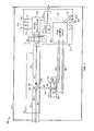
Fig. 1 is a system diagram illustrating an example of a small-form-factor (SFF) fiber optic transceiver module having BIT capabilities with a single input/output (I/O) fiber. -
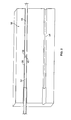
Fig. 2 illustrates a perspective view of a coupler holding and aligning first and second optical fibers of a fiber optic transceiver module with BIT capabilities. -
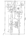
Fig. 3 is a system diagram illustrating an alternative example of a SFF fiber optic transceiver module having BIT capabilities with two fibers, with one fiber transmitting and another fiber receiving optical communication signals. - A fiber optic transceiver module having built-in test capabilities (BIT), and associated method for detecting discontinuities (such as breaks) in the optical fiber that are connected to the transceiver module are provided. An optical source emits an optical signal that is reflected by an angled end of the optical fiber. A portion of the optical signal is received at a second optical fiber and is propagated along the second optical fiber. The second optical fiber has an angled end that is aligned with the angled end of the first optical fiber. If the portion of optical signal propagating along the second optical fiber encounters a discontinuity in the optical path of the second optical fiber, at least a portion of this optical signal is reflected along the second optical fiber back towards the angled end. When the reflected return optical signal reaches the angled end of the second optical fiber, some portion of the reflected return signal is reflected and passed through the angled end and is received by an optical detector. By analyzing the time that has elapsed from the emission of the optical signal by the optical source to the reflected return optical signal pulse detected by the optical detector, the existence and location of the discontinuity may be determined. The use of angled ends in the optical fibers enables the fiber optic transceiver module to achieve BIT functionality while meeting SFF requirements without using bulky optical components to split the optical signals, such as prisms and lenses.
- In particular, a SFF fiber optic transceiver module having BIT capabilities employs a pair of fiber optic cables having their respective ends held and aligned, in a groove of a silicon coupler. A first optical fiber has an angled end that defines an acute angle relative to a longitudinal axis of the first optical fiber. The second optical fiber also has an angled end that defines an acute angle relative to a longitudinal axis of the second optical fiber. The angled ends of the first and second optical fibers are matingly aligned with one another. The acute angle for both the angled ends of the first and second optical fibers, may, for example, both be between 40 degrees and 60 degrees. In one example, the acute angle for both the first and the second optical fibers is 49 degrees. An optical source emits an optical signal that is propagated along the first optical fiber. The optical signal is split at the angled end of the first optical fiber such that a portion of the optical signal is received at the second optical fiber and is propagated along the second optical fiber. An optical detector receives a return optical signal through the angled end of the second optical fiber in response to reflection from a discontinuity in the second optical fiber and the fiber segments that are connected to it.
- Referring to
Fig. 1 , fiberoptic transceiver module 10 is shown. In this example, fiberoptic transceiver module 10 is a SFF transceiver module such that SFF requirements are met in addition to having BIT functionality. As seen inFig. 1 ,optical source 12, such as a vertical cavity surface emitting laser (VCSEL), is disposed withinhousing 14 and emits anoptical signal 16 that is propagated along firstoptical fiber 18. Housed within fiberoptic transceiver module 10 is a printed wiring board (PWB) 20 havingVCSEL driver circuit 22, optical time domain reflectometer (OTDR) signal processing integrated circuit (IC) 24,processor 26, andpost amplifier circuit 28. The components of fiberoptic transceiver module 10 are packaged such that SFF requirements are met. For instance, examples of SFF requirements are 2 x 5, 6 or 7 dual-in-line package (DIP), 0.55" x 2.5" x 0.35" package dimensions, 3.3 volt power supply, as well as other technical requirements. VCSEL 12 is held onsubmount 30 and is controlled bydriver circuit 22, which may be an ASIC. However, theoptical source 12 may be controlled or activated in many other manners. Alternative optical sources, such as edge emitting laser diode, may also be employed. Firstoptical fiber 18 is generally a short fiber used to coupleoptical signal 16 from VCSEL 12. Firstoptical fiber 18 is positioned to receiveoptical signal 16 and transmit the optical signal to secondoptical fiber 32. Secondoptical fiber 32 is generally a long fiber (e.g. 1 meter length) and it is used to form a fiber pigtail to couple optical signals into and out of thetransceiver module 10. Secondoptical fiber 32 extends outside of thehousing 14 and may be used to carry a portion ofoptical signal 34 to another transceiver (not shown) in the fiber cable plant of an airplane. - As shown, first
optical fiber 18 has angledend 36 that defines anacute angle 38 relative to a longitudinal axis of the first optical fiber. Similarly, secondoptical fiber 32 has angledend 40 that defines anacute angle 42 relative to a longitudinal axis of the second optical fiber. The angled ends 36, 40 may be disposed at an angle of between approximately 40 degrees and 60 degrees relative to the longitudinal axis of their corresponding optical fiber. As seen inFig. 1 , theangled end 36 of firstoptical fiber 18 is aligned to be substantially parallel with theangled end 40 of secondoptical fiber 32. In this example, theacute angle 38 for the firstoptical fiber 18 and theacute angle 42 for the secondoptical fiber 32 may be the same. For example, theacute angle 38 for theangled end 36 of firstoptical fiber 18 and theacute angle 42 for theangled end 40 of the secondoptical fiber 32 may both be approximately 49 degrees. - The
acute angle 38 of theangled end 36 of the firstoptical fiber 18 is selected to cause a predefined portion ofoptical signal 16 emitted fromVCSEL 12 to be received at and propagated along secondoptical fiber 32.Angled end 36 of firstoptical fiber 18 splits theoptical signal 16 such that approximately fifty percent of the optical signal coupled fromVCSEL 12 passes from firstoptical fiber 18 is received at secondoptical fiber 32, when an angle of approximately 49 degrees is employed. A portion ofoptical signal 34 is then carried along the secondoptical fiber 32, which may be connected externally to another transceiver (not shown) through the fiber optic cable plant. Secondoptical fiber 32 may exit the housing, for example, through a hermetically sealed feed-through, or by connectorization. If there is a discontinuity in the optical path of the second optical fiber (such as a break), a reflected returnoptical signal 46 returns to theangled end 40 of the secondoptical fiber 32.Optical detector 52 receives the returnoptical signal 54 reflected by theangled end 40 of the secondoptical fiber 32, this reflected signal is from a discontinuity in the optical path of the secondoptical fiber 32. When employing a 49 degree interface, approximately fifty percent of the returnoptical signal 46 is reflected from theangled end 40 of the secondoptical fiber 32 to theoptical detector 52. - Referring to
Fig. 2 ,coupler 56 embeds and aligns the twooptical fibers Coupler 56 may be formed of a silicon material. Formed withincoupler 56 isgroove 58 that may, for instance be V-shaped to hold and align theends optical fibers groove 58 ofsilicon coupler 56. However, other types of optical fibers may selectively be employed. When the two embedded angled fibers ingroove 58 split the optical power equally, the completed structure may be called a 3 dB silicon V-groove coupler. In this example, a 3 dB coupler is a miniaturized 3 dB coupler which allows the BIT transceiver module to be fabricated under the small dimensional requirements of a SFF transceiver. Thesilicon coupler 56 has a short fiber section holding firstoptical fiber 18 coupling directly toVCSEL 12 and a long section holdingangled end 40 of the long secondoptical fiber 32 that forms the pigtail of the transceiver. The pair ofoptical fibers groove 58 of thecoupler 56. In one example, the coating of the shorter firstoptical fiber 18 may be removed, with the first optical fiber embedded in the V-shapedgroove 58. The coating of the secondoptical fiber 32 may also be stripped from the area proximate theangled end 40. To provide strain relief for the secondoptical fiber 32, the V-shapedgroove 58 of thecoupler 56 may include a region having a wider opening for embedding the coated section of the longer secondoptical fiber 32. An epoxy may be used to hold theoptical fibers groove 58. A portion of the secondoptical fiber 32 may extend outward from the end of V-shapedgroove 58 to the outside ofhousing 14 to form the fiber pigtail of the BIT transceiver. - Referring again to
Fig. 1 , if there is a discontinuity in the secondoptical fiber 32 or the fiber segments that are connected to it (the discontinuity is not shown in the figures), a reflected returnoptical signal 46 returns to theangled end 40 of the second optical fiber. A portion of the returnoptical signal 46 is reflected on to theoptical detector 52. For instance, in the example where anangled end 40 of approximately 49 degrees is employed for secondoptical fiber 32, approximately fifty percent of the returnoptical signal 46 is reflected from theangled end 40 of second optical fiber tooptical detector 52.Optical detector 52 may comprise a photodetector, such as a p-type-intrinsic-n-type (PIN) photodiode, an avalanche photodiode, or any other suitable photo detector known to those skilled in the art. In the example shown inFig. 1 ,optical detector 52 haslens 60 for focusing the reflected returnoptical signal 54 on toPIN detector 62 that is coupled with transimpedance amplifier (TIA) integrated circuit (IC) 64. In this example,optical signal 54 is a portion of the returnoptical signal 46 reflected byangled end 40 of secondoptical fiber 32 onto theoptical detector 52 which has itsoptical axis 63 positioned at approximately 90 degrees to the silicon V-groove 58 surface (seeFig. 2 ) of thesilicon coupler 56. This positioning of approximately 90 degrees in relation to the returnoptical signal 46 allows theoptical detector 52 to be easily aligned to detect the reflected signal from the discontinuity or breaks in the optical fibers located in the cable plant.Optical detector 52 may be mounted on a submount 66 (the combination of theoptical detector 52 withphotodiode 62,TIA 64 and thesubmount 66 may be referred to as a receiver optical subassembly) to aid in alignment of the optical detector to the reflectedsignal 54. - Return
optical signal 54 reflected by the discontinuity is received by theoptical detector 52. Theoptical detector 52 provides an output representative of the received signal. TheTIA 64 functions as a pre-amplifier of the detected reflected returnoptical signal 54. The (differential) electrical outputs associated with theTIA 64 are coupled to postamplifier circuit 28 on the transceiver printed wiring board (PWB) 20 using, for example, coax cable or high bandwidth flexible (flex)circuit 68. The differential electrical outputs of thepost amplifier circuit 28 are connected to the Rx+ and Rx-pins 70 of thePWB 20. The electrical output of theoptical detector 52 is transmitted via thepost amplifier circuit 28 to theOTDR IC 24. TheOTDR IC 24 may comprise an application specific integrated circuit (ASIC) or a field programmable gate array (FPGA). Either an ASIC or a FPGA will occupy only small dimensions inPWB 20 of theBIT transceiver module 10. - The
OTDR IC 24 analyzes the signal from theoptical detector 52 to determine the location of the discontinuity along the optical path of secondoptical fiber 32. TheOTDR IC 24, in response to receipt of the output from theoptical detector 52, determines an elapsed time between emission of theoptical signal 16 and receipt of the returnoptical signal 54. For example, a narrow electrical pulse is applied at transmitter inputs (Tx+ and Tx-) 72 coupled withVCSEL driver circuit 22.VCSEL 12 generatesoptical signal 16, which propagates along firstoptical fiber 18 with a portion of the signal carried along secondoptical fiber 32. - In the example seen in
Fig. 1 ,OTDR IC 24,VCSEL driver circuit 22,processor 20 andpost amplifier circuit 28 are mounted on thePWB 20 of the fiberoptic transceiver module 10.Processor 26 is coupled withOTDR IC 24 and may be employed for sending anelectrical signal output 74 to a remote computer (not shown).Processor 26 is the interface between the fiberoptic transceiver module 10 and the flight control (or avionics) computer of the airplane.Processor 26 reports the location of the fiber damage that has been detected by theOTDR IC 24. At the command of the remote flight control computer,processor 26 directs the BIT transceiver to perform either fiber fault detection functions or perform normal data communication operations.Processor 26 may also be equipped with software programs to perform self diagnostics on various components of the fiber optic transceiver module. Therefore, after the BIT capability is incorporated,processor 26 has the overall capability to monitor the health of the fiber optic link in the avionics network of an airplane. - The
OTDR IC 24, coupled withprocessor 26 andVCSEL driver circuit 22, determines the time difference (td) between the optical pulse signals 16 (transmitted by VCSEL 12) and theoptical signal pulse 54 detected bydetector 52. The speed of the light pulse in the optical fiber is equal to the speed of light in free space, c, divided by the fiber index of reflection, nf, (or group index), both are know physical parameters, td is the round trip travel time of the optical pulse from theVCSEL 12 to the discontinuity of the fibers in the optical path of 46. Where c is approximately equal to 3 x10⁸ meters/second, nf is approximately 1.48 in the optical fiber. The location of the discontinuity from the BIT fiber optic transceiver module is determined byOTDR IC 24 as (td x c)/(2 x nf). Knowing the approximate location of the discontinuity allows maintenance personnel to quickly access and repair or replace the damaged optical fiber. If the optical detector does not receive an unexpected reflected pulse within a predefined time period, then there is likely no damage within the optical fiber. - Referring to
Fig. 3 , an alternative example of a SFF fiberoptic transceiver module 10 is shown. Certain platforms may use duplex fiber optic networks with fiber optic transceiver modules using separate optical fibers for the transmission and the receiving of optical signals. In the embodiment seen inFig. 3 ,optical fibers optical fiber 80 is employed which acts as a separate receive optical fiber. The receiveoptical fiber 80, positioned onfiber locking pedestal 81, propagates a receiveoptical signal 82 received from a corresponding transmitter of a fiber optic transceiver (not shown) of a remote fiber optic network node. In this example, a receiver optical detector 84 (such as another PIN detector coupled with a transimpedance amplifier) is added to the fiberoptic transceiver module 10 with receiveroptical detector 84 coupled withpost amplifier circuit 28. To conserve space for the receiveoptical fiber 80 and the additional receiveroptical detector 84, theoptical detector 52 is coupled toOTDR IC 24 in thePWB 20 by a thin high bandwidth flexibleoptical ribbon cable 86. The process for detecting discontinuities in the optical path of secondoptical fiber 32 is similar to the operation as set forth inFig. 1 . In the configuration ofFig. 3 , receiveroptical detector 84 is connected to postamplifier circuit 28, andoptical fiber VCSEL 12. Detection of discontinuities in the cable plant is made upon receipt of the return optical signal tooptical detector 52 coupled byflex circuit 86 toOTDR IC 24, in the example seen inFig. 3 . - The foregoing description of the preferred embodiments of the invention have been presented for purposes of illustration and description, and are not intended to be exhaustive or to limit the invention the precise forms disclosed. The descriptions were selected to best explain the principles of the invention and their practical application to enable others skilled in the art to best utilize the invention in various embodiments and various modifications as are suited to the particular use contemplated. It is intended that the scope of the invention not be limited by the specification, but be defined by the claims set forth below.
Claims (19)
- A fiber optic transceiver module having built-in test capabilities comprising:a first optical fiber (19) having an angled end (36) that defines an acute angle relative to a longitudinal axis of the first optical fiber;a second optical fiber (32) having an angled end (40) that defines an acute angle relative to a longitudinal axis of the second optical fiber, the first optical fiber and the second optical fiber being aligned with one another;an optical source (12) that emits an optical signal (16) propagated along the first optical fiber in which a portion of the optical signal (34) is received at the second optical fiber and is propagated along the second optical fiber; andan optical detector (52) for receiving a return optical signal (54) from the angled end of the second optical fiber in response to reflection from a discontinuity in an optical path of the second optical fiber.
- The fiber optic transceiver module of claim 1, wherein the acute angle (38) for the angled end (36) of the first optical fiber (18) and the acute angle (42) for the angled end (40) of the second optical fiber (32) are both between 40 degrees and 60 degrees.
- The fiber optic transceiver module of claim 2, wherein the angled end of the first optical fiber is aligned to be substantially parallel with the angled end of the second optical fiber.
- The fiber optic transceiver module of claim 2, wherein the acute angle (38) of the angled end of the first optical fiber (18) is selected to cause a predefined portion of the optical signal (16) emitted from the optical source to be received at and propagated along the second optical fiber (32).
- The fiber optic transceiver module of claim 4, wherein approximately 50 percent of the optical signal (16) coupled from the optical source is passed from the first optical fiber (18) to the second optical fiber (32).
- The fiber optic transceiver module of claim 5, wherein approximately 50 percent of the return optical signal (46) is reflected from the angled end of the second optical fiber (32) to the optical detector (52).
- The fiber optic transceiver module of any preceding claim, further comprising a coupler (56) having a groove (58) that holds and aligns the first optical fiber (18) and the second optical fiber (32).
- The fiber optic transceiver module of claim 7, wherein the coupler is formed of silicon material and the groove is V-shaped.
- The fiber optic transceiver module of any preceding claim, wherein the fiber optic transceiver module meets small-form-factor requirements.
- The fiber optic transceiver module of any preceding claim, wherein the optical source (12) comprises a vertical cavity surface emitting laser.
- The fiber optic transceiver module of claim 10, wherein the optical detector (52) comprises a p-type-intrinsic-n-type (PIN) detector (62) coupled with a transimpedance amplifier circuit (64).
- The fiber optic transceiver module of claim 10, further comprising an optical time domain reflectometer (OTDR) integrated circuit (IC) (24), responsive to the optical detector (52), for determining an elapsed time between emission of the optical signal and receipt of the return optical signal.
- The fiber optic transceiver module of claim 12, further comprising a processor (26) coupled with the OTDR IC (24) for sending electrical signal output (74) to a remote computer.
- The fiber optic transceiver module of claim 13, wherein the OTDR IC (24), a driver circuit of the vertical cavity surface emitting laser (22), and the processor (26) are mounted on a printed wiring board (20) of the fiber optic transceiver module.
- The fiber optic transceiver module of any preceding claim, further comprising a separate receive optical fiber (80) for propagating optical signals (82) received from a transmitter in a remote fiber optic network node.
- A method for detecting discontinuities in a fiber optic transceiver module having built-in test capabilities, comprising:emitting an optical signal (16) propagated along a first optical fiber (18) having an angled end that defines an acute angle (38) relative to a longitudinal axis of the first optical fiber, such that a portion of the optical signal is received at and propagated along a second optical fiber (32), the second optical fiber having an angled end that defines an acute angle (42) relative to a longitudinal axis of the second optical fiber, the angled end of the first optical fiber aligned with the angled end of the second optical fiber; andreceiving a return optical signal (46) through the angled end of the second optical fiber by an optical detector (52) in response to reflection from a discontinuity in an optical path of the second optical fiber.
- The method of claim 16, wherein the acute angle of the angled end of the first optical fiber (18) is selected to cause a predefined portion of the optical signal (34) emitted from the optical source to be received at and propagated along the second optical fiber (32).
- The method of claim 16 or 17, further comprising determining an elapsed time between emission of the optical signal (16) and receipt of the return optical signal (54), such that a location of the discontinuity along the optical path of the second optical fiber may be determined.
- The method of any of claims 16-18, further comprising employing a separate receive optical fiber (80) for propagating optical signals (82) received from a transmitter in a remote fiber optic network node.
Applications Claiming Priority (1)
| Application Number | Priority Date | Filing Date | Title |
|---|---|---|---|
| US11/555,354 US7484899B2 (en) | 2006-11-01 | 2006-11-01 | Small-form-factor fiber optic transceiver module having built-in test capability and method |
Publications (2)
| Publication Number | Publication Date |
|---|---|
| EP1918747A1 true EP1918747A1 (en) | 2008-05-07 |
| EP1918747B1 EP1918747B1 (en) | 2017-01-25 |
Family
ID=39030815
Family Applications (1)
| Application Number | Title | Priority Date | Filing Date |
|---|---|---|---|
| EP07254187.3A Active EP1918747B1 (en) | 2006-11-01 | 2007-10-22 | Small-form-factor fiber optic transceiver module having built-in test capability and method |
Country Status (2)
| Country | Link |
|---|---|
| US (1) | US7484899B2 (en) |
| EP (1) | EP1918747B1 (en) |
Cited By (1)
| Publication number | Priority date | Publication date | Assignee | Title |
|---|---|---|---|---|
| US10305587B2 (en) | 2014-05-09 | 2019-05-28 | Sikorsky Aircraft Corporation | Method and apparatus for condition based maintenance of fiber networks on vehicles |
Families Citing this family (11)
| Publication number | Priority date | Publication date | Assignee | Title |
|---|---|---|---|---|
| WO2011053306A1 (en) * | 2009-10-30 | 2011-05-05 | Hewlett-Packard Development Company, L.P. | Optical transceiver having an otdr mode, and a method of obtaining test data for testing an optical fiber |
| US8666254B2 (en) | 2011-04-26 | 2014-03-04 | The Boeing Company | System and method of wireless optical communication |
| WO2013162903A2 (en) * | 2012-04-11 | 2013-10-31 | Ultra Communications, Inc. | Optical time domain reflectometer in a small form factor package |
| US9245443B2 (en) | 2013-02-21 | 2016-01-26 | The Boeing Company | Passenger services system for an aircraft |
| WO2015097490A1 (en) * | 2013-12-27 | 2015-07-02 | Intel Corporation | Display having an integrated camera |
| US20160334591A1 (en) | 2015-05-14 | 2016-11-17 | Lockheed Martin Corporation | Space active optical cable |
| EP3297093B1 (en) * | 2016-09-16 | 2019-01-02 | Rosenberger Hochfrequenztechnik GmbH & Co. KG | Connector for connecting an optical fiber and an electrical conductor |
| US10230459B2 (en) | 2017-02-14 | 2019-03-12 | The Boeing Company | System and method for optical time-domain reflectometry and design data wire testing |
| US9948403B1 (en) | 2017-02-28 | 2018-04-17 | International Business Machines Corporation | Network fiber optic cable connector with magnetic contacts |
| US10075232B1 (en) | 2017-04-18 | 2018-09-11 | Cisco Technology, Inc. | Detecting fiber optic breaks using autonomous vehicles |
| US12687458B2 (en) * | 2022-08-25 | 2026-07-21 | Ii-Vi Delaware, Inc. | Pluggable optical time domain reflectometer |
Citations (7)
| Publication number | Priority date | Publication date | Assignee | Title |
|---|---|---|---|---|
| US4165496A (en) | 1977-12-16 | 1979-08-21 | Bell Telephone Laboratories, Incorporated | Optical fiber light tap |
| GB2020447A (en) * | 1978-05-09 | 1979-11-14 | Plessey Co Ltd | Optical fibre branching arrangements |
| US5416869A (en) * | 1992-03-19 | 1995-05-16 | Nec Corporation | Semiconductor laser/optical fiber coupling device |
| EP1008880A2 (en) | 1998-12-09 | 2000-06-14 | Matsushita Electric Industrial Co., Ltd. | Optical communications module and method for mounting optical communications module |
| EP1154299A1 (en) | 1999-09-28 | 2001-11-14 | Sumitomo Electric Industries, Ltd. | Optical communications device |
| US20040017978A1 (en) * | 2002-07-25 | 2004-01-29 | Yoshiki Kuhara | Optical module |
| US20060228078A1 (en) | 2005-03-30 | 2006-10-12 | The Boeing Company | Fiber optic transceiver module having built-in test capability and associated method |
Family Cites Families (17)
| Publication number | Priority date | Publication date | Assignee | Title |
|---|---|---|---|---|
| FR2389883B1 (en) * | 1977-05-05 | 1980-07-25 | Cselt Centro Studi Lab Telecom | |
| JPS5948447B2 (en) * | 1977-07-20 | 1984-11-27 | ソニー株式会社 | Gain compensation circuit for signal regenerator |
| CA1154299A (en) | 1980-07-08 | 1983-09-27 | Daniel Kerwin | Method and apparatus for applying decals to articles |
| US5071213A (en) * | 1990-10-31 | 1991-12-10 | The Boeing Company | Optical coupler and method of making optical coupler |
| US5841562A (en) * | 1995-12-28 | 1998-11-24 | Lucent Technologies, Inc. | Bidirectional modular optoelectronic transceiver assembly |
| US5896481A (en) * | 1997-05-30 | 1999-04-20 | The Boeing Company | Optical subassembly with a groove for aligning an optical device with an optical fiber |
| US6704515B1 (en) * | 1999-12-30 | 2004-03-09 | The Boeing Company | Fiber optic interface module and associated fabrication method |
| US6821027B2 (en) * | 2000-10-16 | 2004-11-23 | Opti Japan Corporation | Miniaturized parallel optical transmitter and receiver module |
| CN100529816C (en) * | 2001-11-15 | 2009-08-19 | 派克米瑞斯公司 | Focusing fiber optic |
| US6760502B2 (en) * | 2001-12-04 | 2004-07-06 | Lucent Technologies Inc. | Power monitoring arrangement for optical cross-connect systems |
| JP3750649B2 (en) * | 2001-12-25 | 2006-03-01 | 住友電気工業株式会社 | Optical communication device |
| US7171081B1 (en) * | 2002-03-14 | 2007-01-30 | Lightech Fiberoptics, Inc. | Plug-in coupler to convert the transceiver (transmitter/receiver, tx/rx) transmission into a bi-directional fiber |
| US6873780B2 (en) * | 2002-06-21 | 2005-03-29 | The Boeing Company | Method for fabricating an array of optical fibers having angled end faces |
| US7031574B2 (en) * | 2002-07-10 | 2006-04-18 | Finisar Corporation | Plug-in module for providing bi-directional data transmission |
| EP1576385A2 (en) * | 2002-11-26 | 2005-09-21 | James F. Munro | An apparatus for high accuracy distance and velocity measurement and methods thereof |
| US20050129367A1 (en) * | 2003-12-12 | 2005-06-16 | The Boeing Company, A Delaware Corporation | Method and apparatus for angled fiber optical attenuation |
| US7654750B2 (en) * | 2005-08-10 | 2010-02-02 | Brenner Mary K | Bidirectional optical fiber link systems component couplers |
-
2006
- 2006-11-01 US US11/555,354 patent/US7484899B2/en active Active
-
2007
- 2007-10-22 EP EP07254187.3A patent/EP1918747B1/en active Active
Patent Citations (7)
| Publication number | Priority date | Publication date | Assignee | Title |
|---|---|---|---|---|
| US4165496A (en) | 1977-12-16 | 1979-08-21 | Bell Telephone Laboratories, Incorporated | Optical fiber light tap |
| GB2020447A (en) * | 1978-05-09 | 1979-11-14 | Plessey Co Ltd | Optical fibre branching arrangements |
| US5416869A (en) * | 1992-03-19 | 1995-05-16 | Nec Corporation | Semiconductor laser/optical fiber coupling device |
| EP1008880A2 (en) | 1998-12-09 | 2000-06-14 | Matsushita Electric Industrial Co., Ltd. | Optical communications module and method for mounting optical communications module |
| EP1154299A1 (en) | 1999-09-28 | 2001-11-14 | Sumitomo Electric Industries, Ltd. | Optical communications device |
| US20040017978A1 (en) * | 2002-07-25 | 2004-01-29 | Yoshiki Kuhara | Optical module |
| US20060228078A1 (en) | 2005-03-30 | 2006-10-12 | The Boeing Company | Fiber optic transceiver module having built-in test capability and associated method |
Non-Patent Citations (2)
| Title |
|---|
| 2006 IEEE/AIAA 25TH DIGITAL AVIONICS SYSTEMS CONFERENCE 15-19 OCT. 2006 PORTLAND, OR, USA, 15 October 2006 (2006-10-15) - 19 October 2006 (2006-10-19), 2006 IEEE/AIAA 25th Digital Avionics Systems Conference (IEEE Cat No. 06CH37804) IEEE Piscataway, NJ, USA, pages 4 pp., ISBN: 1-4244-0378-2 * |
| DATABASE INSPEC [online] THE INSTITUTION OF ELECTRICAL ENGINEERS, STEVENAGE, GB; 19 October 2006 (2006-10-19), CHAN E Y ET AL: "Demonstration of a Gb/s transceiver with OTDR built-in-test for avionics local area networks", XP031048469, Database accession no. 9443178 * |
Cited By (1)
| Publication number | Priority date | Publication date | Assignee | Title |
|---|---|---|---|---|
| US10305587B2 (en) | 2014-05-09 | 2019-05-28 | Sikorsky Aircraft Corporation | Method and apparatus for condition based maintenance of fiber networks on vehicles |
Also Published As
| Publication number | Publication date |
|---|---|
| EP1918747B1 (en) | 2017-01-25 |
| US20080101752A1 (en) | 2008-05-01 |
| US7484899B2 (en) | 2009-02-03 |
Similar Documents
| Publication | Publication Date | Title |
|---|---|---|
| EP1918747B1 (en) | Small-form-factor fiber optic transceiver module having built-in test capability and method | |
| CA2222845C (en) | An inexpensive single-fiber bidirectional data link | |
| US7093985B2 (en) | Wall mount fiber optic connector and associated method for forming the same | |
| US9036991B2 (en) | Optical transceiver having an OTDR mode, and a method of obtaining test data for testing an optical fiber | |
| US6185346B1 (en) | Propagation in lowest order modes of multimode graded index fiber, resulting in: very low transmission loss, low modal noise, high data security, and high data rate capabilities | |
| US5600470A (en) | Mixed fiber adapter cable | |
| US20070036493A1 (en) | Bidirectional optical fiber link systems components couplers | |
| US7341384B2 (en) | Fiber optic transceiver module having built-in test capability and associated method | |
| US20190140761A1 (en) | Bidirectional, Multi-Wavelength Gigabit Optical Fiber Network | |
| US7309169B2 (en) | Single-channel communication device for optical fibre | |
| US20140226991A1 (en) | Dual-Wavelength Bidirectional Optical Communication System and Method for Communicating Optical Signals | |
| US6630992B1 (en) | Method and device for executing control and monitoring measurements in optical transmission paths | |
| CN110311733A (en) | Single-Wavelength Bidirectional Transceiver with Integrated Fiber Coupler | |
| US20140217270A1 (en) | Light-receiving module | |
| US5008545A (en) | High resolution optical fault locator | |
| Kuznia et al. | Novel high-resolution OTDR technology for multi-Gbps transceivers | |
| RU2717374C2 (en) | Optical bench subassembly having integrated photonic device | |
| EP4345518B1 (en) | Apparatus and method for low latency free-space optical communications | |
| US20090060529A1 (en) | Optical bench fiber optic transmitter | |
| CN118400028A (en) | Optical time domain reflectometer system | |
| Curran et al. | Basics of fiber optics | |
| US7684695B1 (en) | Optical diagnostic indicator | |
| CN120677364A (en) | Method and device for measuring inter-space channel crosstalk | |
| US8023784B1 (en) | Optical subassembly package configuration | |
| CN211042472U (en) | Optical fiber vibration sensor |
Legal Events
| Date | Code | Title | Description |
|---|---|---|---|
| PUAI | Public reference made under article 153(3) epc to a published international application that has entered the european phase |
Free format text: ORIGINAL CODE: 0009012 |
|
| 17P | Request for examination filed |
Effective date: 20071102 |
|
| AK | Designated contracting states |
Kind code of ref document: A1 Designated state(s): AT BE BG CH CY CZ DE DK EE ES FI FR GB GR HU IE IS IT LI LT LU LV MC MT NL PL PT RO SE SI SK TR |
|
| AX | Request for extension of the european patent |
Extension state: AL BA HR MK RS |
|
| 17Q | First examination report despatched |
Effective date: 20081215 |
|
| AKX | Designation fees paid |
Designated state(s): AT BE BG CH CY CZ DE DK EE ES FI FR GB GR HU IE IS IT LI LT LU LV MC MT NL PL PT RO SE SI SK TR |
|
| GRAP | Despatch of communication of intention to grant a patent |
Free format text: ORIGINAL CODE: EPIDOSNIGR1 |
|
| RIC1 | Information provided on ipc code assigned before grant |
Ipc: G01M 11/00 20060101ALI20160224BHEP Ipc: G02B 6/42 20060101AFI20160224BHEP |
|
| INTG | Intention to grant announced |
Effective date: 20160317 |
|
| GRAJ | Information related to disapproval of communication of intention to grant by the applicant or resumption of examination proceedings by the epo deleted |
Free format text: ORIGINAL CODE: EPIDOSDIGR1 |
|
| GRAP | Despatch of communication of intention to grant a patent |
Free format text: ORIGINAL CODE: EPIDOSNIGR1 |
|
| INTC | Intention to grant announced (deleted) | ||
| INTG | Intention to grant announced |
Effective date: 20160816 |
|
| GRAS | Grant fee paid |
Free format text: ORIGINAL CODE: EPIDOSNIGR3 |
|
| GRAA | (expected) grant |
Free format text: ORIGINAL CODE: 0009210 |
|
| AK | Designated contracting states |
Kind code of ref document: B1 Designated state(s): AT BE BG CH CY CZ DE DK EE ES FI FR GB GR HU IE IS IT LI LT LU LV MC MT NL PL PT RO SE SI SK TR |
|
| REG | Reference to a national code |
Ref country code: GB Ref legal event code: FG4D |
|
| REG | Reference to a national code |
Ref country code: CH Ref legal event code: EP |
|
| REG | Reference to a national code |
Ref country code: AT Ref legal event code: REF Ref document number: 864462 Country of ref document: AT Kind code of ref document: T Effective date: 20170215 |
|
| REG | Reference to a national code |
Ref country code: IE Ref legal event code: FG4D |
|
| REG | Reference to a national code |
Ref country code: DE Ref legal event code: R096 Ref document number: 602007049629 Country of ref document: DE |
|
| REG | Reference to a national code |
Ref country code: LT Ref legal event code: MG4D |
|
| REG | Reference to a national code |
Ref country code: NL Ref legal event code: MP Effective date: 20170125 |
|
| REG | Reference to a national code |
Ref country code: AT Ref legal event code: MK05 Ref document number: 864462 Country of ref document: AT Kind code of ref document: T Effective date: 20170125 |
|
| PG25 | Lapsed in a contracting state [announced via postgrant information from national office to epo] |
Ref country code: NL Free format text: LAPSE BECAUSE OF FAILURE TO SUBMIT A TRANSLATION OF THE DESCRIPTION OR TO PAY THE FEE WITHIN THE PRESCRIBED TIME-LIMIT Effective date: 20170125 |
|
| PG25 | Lapsed in a contracting state [announced via postgrant information from national office to epo] |
Ref country code: GR Free format text: LAPSE BECAUSE OF FAILURE TO SUBMIT A TRANSLATION OF THE DESCRIPTION OR TO PAY THE FEE WITHIN THE PRESCRIBED TIME-LIMIT Effective date: 20170426 Ref country code: FI Free format text: LAPSE BECAUSE OF FAILURE TO SUBMIT A TRANSLATION OF THE DESCRIPTION OR TO PAY THE FEE WITHIN THE PRESCRIBED TIME-LIMIT Effective date: 20170125 Ref country code: LT Free format text: LAPSE BECAUSE OF FAILURE TO SUBMIT A TRANSLATION OF THE DESCRIPTION OR TO PAY THE FEE WITHIN THE PRESCRIBED TIME-LIMIT Effective date: 20170125 Ref country code: IS Free format text: LAPSE BECAUSE OF FAILURE TO SUBMIT A TRANSLATION OF THE DESCRIPTION OR TO PAY THE FEE WITHIN THE PRESCRIBED TIME-LIMIT Effective date: 20170525 |
|
| PG25 | Lapsed in a contracting state [announced via postgrant information from national office to epo] |
Ref country code: AT Free format text: LAPSE BECAUSE OF FAILURE TO SUBMIT A TRANSLATION OF THE DESCRIPTION OR TO PAY THE FEE WITHIN THE PRESCRIBED TIME-LIMIT Effective date: 20170125 Ref country code: SE Free format text: LAPSE BECAUSE OF FAILURE TO SUBMIT A TRANSLATION OF THE DESCRIPTION OR TO PAY THE FEE WITHIN THE PRESCRIBED TIME-LIMIT Effective date: 20170125 Ref country code: PL Free format text: LAPSE BECAUSE OF FAILURE TO SUBMIT A TRANSLATION OF THE DESCRIPTION OR TO PAY THE FEE WITHIN THE PRESCRIBED TIME-LIMIT Effective date: 20170125 Ref country code: ES Free format text: LAPSE BECAUSE OF FAILURE TO SUBMIT A TRANSLATION OF THE DESCRIPTION OR TO PAY THE FEE WITHIN THE PRESCRIBED TIME-LIMIT Effective date: 20170125 Ref country code: LV Free format text: LAPSE BECAUSE OF FAILURE TO SUBMIT A TRANSLATION OF THE DESCRIPTION OR TO PAY THE FEE WITHIN THE PRESCRIBED TIME-LIMIT Effective date: 20170125 Ref country code: PT Free format text: LAPSE BECAUSE OF FAILURE TO SUBMIT A TRANSLATION OF THE DESCRIPTION OR TO PAY THE FEE WITHIN THE PRESCRIBED TIME-LIMIT Effective date: 20170525 Ref country code: BG Free format text: LAPSE BECAUSE OF FAILURE TO SUBMIT A TRANSLATION OF THE DESCRIPTION OR TO PAY THE FEE WITHIN THE PRESCRIBED TIME-LIMIT Effective date: 20170425 |
|
| REG | Reference to a national code |
Ref country code: FR Ref legal event code: PLFP Year of fee payment: 11 |
|
| REG | Reference to a national code |
Ref country code: DE Ref legal event code: R097 Ref document number: 602007049629 Country of ref document: DE |
|
| PG25 | Lapsed in a contracting state [announced via postgrant information from national office to epo] |
Ref country code: SK Free format text: LAPSE BECAUSE OF FAILURE TO SUBMIT A TRANSLATION OF THE DESCRIPTION OR TO PAY THE FEE WITHIN THE PRESCRIBED TIME-LIMIT Effective date: 20170125 Ref country code: RO Free format text: LAPSE BECAUSE OF FAILURE TO SUBMIT A TRANSLATION OF THE DESCRIPTION OR TO PAY THE FEE WITHIN THE PRESCRIBED TIME-LIMIT Effective date: 20170125 Ref country code: CZ Free format text: LAPSE BECAUSE OF FAILURE TO SUBMIT A TRANSLATION OF THE DESCRIPTION OR TO PAY THE FEE WITHIN THE PRESCRIBED TIME-LIMIT Effective date: 20170125 Ref country code: EE Free format text: LAPSE BECAUSE OF FAILURE TO SUBMIT A TRANSLATION OF THE DESCRIPTION OR TO PAY THE FEE WITHIN THE PRESCRIBED TIME-LIMIT Effective date: 20170125 |
|
| PG25 | Lapsed in a contracting state [announced via postgrant information from national office to epo] |
Ref country code: DK Free format text: LAPSE BECAUSE OF FAILURE TO SUBMIT A TRANSLATION OF THE DESCRIPTION OR TO PAY THE FEE WITHIN THE PRESCRIBED TIME-LIMIT Effective date: 20170125 |
|
| PLBE | No opposition filed within time limit |
Free format text: ORIGINAL CODE: 0009261 |
|
| STAA | Information on the status of an ep patent application or granted ep patent |
Free format text: STATUS: NO OPPOSITION FILED WITHIN TIME LIMIT |
|
| 26N | No opposition filed |
Effective date: 20171026 |
|
| PG25 | Lapsed in a contracting state [announced via postgrant information from national office to epo] |
Ref country code: SI Free format text: LAPSE BECAUSE OF FAILURE TO SUBMIT A TRANSLATION OF THE DESCRIPTION OR TO PAY THE FEE WITHIN THE PRESCRIBED TIME-LIMIT Effective date: 20170125 |
|
| PG25 | Lapsed in a contracting state [announced via postgrant information from national office to epo] |
Ref country code: MC Free format text: LAPSE BECAUSE OF FAILURE TO SUBMIT A TRANSLATION OF THE DESCRIPTION OR TO PAY THE FEE WITHIN THE PRESCRIBED TIME-LIMIT Effective date: 20170125 |
|
| REG | Reference to a national code |
Ref country code: CH Ref legal event code: PL |
|
| REG | Reference to a national code |
Ref country code: IE Ref legal event code: MM4A |
|
| PG25 | Lapsed in a contracting state [announced via postgrant information from national office to epo] |
Ref country code: LI Free format text: LAPSE BECAUSE OF NON-PAYMENT OF DUE FEES Effective date: 20171031 Ref country code: CH Free format text: LAPSE BECAUSE OF NON-PAYMENT OF DUE FEES Effective date: 20171031 Ref country code: LU Free format text: LAPSE BECAUSE OF NON-PAYMENT OF DUE FEES Effective date: 20171022 |
|
| REG | Reference to a national code |
Ref country code: BE Ref legal event code: MM Effective date: 20171031 |
|
| PG25 | Lapsed in a contracting state [announced via postgrant information from national office to epo] |
Ref country code: BE Free format text: LAPSE BECAUSE OF NON-PAYMENT OF DUE FEES Effective date: 20171031 |
|
| PG25 | Lapsed in a contracting state [announced via postgrant information from national office to epo] |
Ref country code: MT Free format text: LAPSE BECAUSE OF NON-PAYMENT OF DUE FEES Effective date: 20171022 |
|
| REG | Reference to a national code |
Ref country code: FR Ref legal event code: PLFP Year of fee payment: 12 |
|
| PG25 | Lapsed in a contracting state [announced via postgrant information from national office to epo] |
Ref country code: IE Free format text: LAPSE BECAUSE OF NON-PAYMENT OF DUE FEES Effective date: 20171022 |
|
| PG25 | Lapsed in a contracting state [announced via postgrant information from national office to epo] |
Ref country code: HU Free format text: LAPSE BECAUSE OF FAILURE TO SUBMIT A TRANSLATION OF THE DESCRIPTION OR TO PAY THE FEE WITHIN THE PRESCRIBED TIME-LIMIT; INVALID AB INITIO Effective date: 20071022 |
|
| PG25 | Lapsed in a contracting state [announced via postgrant information from national office to epo] |
Ref country code: CY Free format text: LAPSE BECAUSE OF NON-PAYMENT OF DUE FEES Effective date: 20170125 |
|
| REG | Reference to a national code |
Ref country code: DE Ref legal event code: R082 Ref document number: 602007049629 Country of ref document: DE Representative=s name: MAIER, LL.M., MICHAEL C., DE Ref country code: DE Ref legal event code: R082 Ref document number: 602007049629 Country of ref document: DE Representative=s name: BOULT WADE TENNANT LLP, DE |
|
| REG | Reference to a national code |
Ref country code: DE Ref legal event code: R082 Ref document number: 602007049629 Country of ref document: DE Representative=s name: BOULT WADE TENNANT LLP, DE |
|
| PG25 | Lapsed in a contracting state [announced via postgrant information from national office to epo] |
Ref country code: TR Free format text: LAPSE BECAUSE OF FAILURE TO SUBMIT A TRANSLATION OF THE DESCRIPTION OR TO PAY THE FEE WITHIN THE PRESCRIBED TIME-LIMIT Effective date: 20170125 |
|
| P01 | Opt-out of the competence of the unified patent court (upc) registered |
Effective date: 20230516 |
|
| PGFP | Annual fee paid to national office [announced via postgrant information from national office to epo] |
Ref country code: DE Payment date: 20251029 Year of fee payment: 19 |
|
| PGFP | Annual fee paid to national office [announced via postgrant information from national office to epo] |
Ref country code: GB Payment date: 20251027 Year of fee payment: 19 |
|
| PGFP | Annual fee paid to national office [announced via postgrant information from national office to epo] |
Ref country code: IT Payment date: 20251021 Year of fee payment: 19 |
|
| PGFP | Annual fee paid to national office [announced via postgrant information from national office to epo] |
Ref country code: FR Payment date: 20251027 Year of fee payment: 19 |