EP1918412A1 - Apparatus for selective deposition of graded coatings - Google Patents
Apparatus for selective deposition of graded coatings Download PDFInfo
- Publication number
- EP1918412A1 EP1918412A1 EP07115356A EP07115356A EP1918412A1 EP 1918412 A1 EP1918412 A1 EP 1918412A1 EP 07115356 A EP07115356 A EP 07115356A EP 07115356 A EP07115356 A EP 07115356A EP 1918412 A1 EP1918412 A1 EP 1918412A1
- Authority
- EP
- European Patent Office
- Prior art keywords
- deposition
- coating
- web
- selective
- chamber
- Prior art date
- Legal status (The legal status is an assumption and is not a legal conclusion. Google has not performed a legal analysis and makes no representation as to the accuracy of the status listed.)
- Ceased
Links
- 230000008021 deposition Effects 0.000 title claims abstract description 138
- 238000000576 coating method Methods 0.000 title claims abstract description 101
- 239000011248 coating agent Substances 0.000 claims abstract description 96
- 239000000463 material Substances 0.000 claims description 54
- 230000004888 barrier function Effects 0.000 claims description 16
- 239000011147 inorganic material Substances 0.000 claims description 8
- 239000010409 thin film Substances 0.000 claims description 8
- 238000003491 array Methods 0.000 claims description 6
- 229910010272 inorganic material Inorganic materials 0.000 claims description 6
- 239000004973 liquid crystal related substance Substances 0.000 claims description 5
- 238000004146 energy storage Methods 0.000 claims description 3
- 238000004020 luminiscence type Methods 0.000 claims description 3
- 230000005693 optoelectronics Effects 0.000 claims description 3
- 238000004519 manufacturing process Methods 0.000 abstract description 39
- 238000000034 method Methods 0.000 abstract description 28
- 230000007246 mechanism Effects 0.000 abstract description 11
- 238000000151 deposition Methods 0.000 description 119
- 239000000758 substrate Substances 0.000 description 66
- 239000000203 mixture Substances 0.000 description 24
- 239000010410 layer Substances 0.000 description 18
- 239000007789 gas Substances 0.000 description 12
- 230000008569 process Effects 0.000 description 12
- QVGXLLKOCUKJST-UHFFFAOYSA-N atomic oxygen Chemical compound [O] QVGXLLKOCUKJST-UHFFFAOYSA-N 0.000 description 9
- 230000007547 defect Effects 0.000 description 9
- 239000011521 glass Substances 0.000 description 9
- 229910052760 oxygen Inorganic materials 0.000 description 9
- 239000001301 oxygen Substances 0.000 description 9
- 239000000126 substance Substances 0.000 description 9
- 239000008199 coating composition Substances 0.000 description 8
- 230000007704 transition Effects 0.000 description 8
- 229910052751 metal Inorganic materials 0.000 description 7
- 239000002184 metal Substances 0.000 description 7
- 238000000623 plasma-assisted chemical vapour deposition Methods 0.000 description 7
- 229920005989 resin Polymers 0.000 description 7
- 239000011347 resin Substances 0.000 description 7
- 210000004027 cell Anatomy 0.000 description 6
- 238000005516 engineering process Methods 0.000 description 6
- 239000011368 organic material Substances 0.000 description 6
- 210000002381 plasma Anatomy 0.000 description 6
- BLRPTPMANUNPDV-UHFFFAOYSA-N Silane Chemical compound [SiH4] BLRPTPMANUNPDV-UHFFFAOYSA-N 0.000 description 5
- 239000004033 plastic Substances 0.000 description 5
- 229920003023 plastic Polymers 0.000 description 5
- 239000000376 reactant Substances 0.000 description 5
- XLYOFNOQVPJJNP-UHFFFAOYSA-N water Chemical compound O XLYOFNOQVPJJNP-UHFFFAOYSA-N 0.000 description 5
- QGZKDVFQNNGYKY-UHFFFAOYSA-N Ammonia Chemical compound N QGZKDVFQNNGYKY-UHFFFAOYSA-N 0.000 description 4
- 238000005229 chemical vapour deposition Methods 0.000 description 4
- 238000001723 curing Methods 0.000 description 4
- FFUAGWLWBBFQJT-UHFFFAOYSA-N hexamethyldisilazane Chemical compound C[Si](C)(C)N[Si](C)(C)C FFUAGWLWBBFQJT-UHFFFAOYSA-N 0.000 description 4
- 230000002401 inhibitory effect Effects 0.000 description 4
- VNWKTOKETHGBQD-UHFFFAOYSA-N methane Chemical compound C VNWKTOKETHGBQD-UHFFFAOYSA-N 0.000 description 4
- 239000012044 organic layer Substances 0.000 description 4
- 230000005855 radiation Effects 0.000 description 4
- 239000004065 semiconductor Substances 0.000 description 4
- 229910000077 silane Inorganic materials 0.000 description 4
- 238000004544 sputter deposition Methods 0.000 description 4
- 239000004593 Epoxy Substances 0.000 description 3
- XUIMIQQOPSSXEZ-UHFFFAOYSA-N Silicon Chemical compound [Si] XUIMIQQOPSSXEZ-UHFFFAOYSA-N 0.000 description 3
- 230000000712 assembly Effects 0.000 description 3
- 238000000429 assembly Methods 0.000 description 3
- 230000008901 benefit Effects 0.000 description 3
- 239000000919 ceramic Substances 0.000 description 3
- 210000000078 claw Anatomy 0.000 description 3
- 230000000295 complement effect Effects 0.000 description 3
- 238000013461 design Methods 0.000 description 3
- 238000009792 diffusion process Methods 0.000 description 3
- 229920002457 flexible plastic Polymers 0.000 description 3
- 230000005012 migration Effects 0.000 description 3
- 238000013508 migration Methods 0.000 description 3
- 230000037361 pathway Effects 0.000 description 3
- 229920000647 polyepoxide Polymers 0.000 description 3
- 239000000047 product Substances 0.000 description 3
- 239000010703 silicon Substances 0.000 description 3
- 229910052710 silicon Inorganic materials 0.000 description 3
- IJGRMHOSHXDMSA-UHFFFAOYSA-N Atomic nitrogen Chemical compound N#N IJGRMHOSHXDMSA-UHFFFAOYSA-N 0.000 description 2
- BOTDANWDWHJENH-UHFFFAOYSA-N Tetraethyl orthosilicate Chemical compound CCO[Si](OCC)(OCC)OCC BOTDANWDWHJENH-UHFFFAOYSA-N 0.000 description 2
- 230000004913 activation Effects 0.000 description 2
- 239000000654 additive Substances 0.000 description 2
- 239000000853 adhesive Substances 0.000 description 2
- 239000002390 adhesive tape Substances 0.000 description 2
- 150000001412 amines Chemical class 0.000 description 2
- 229910021529 ammonia Inorganic materials 0.000 description 2
- 238000013459 approach Methods 0.000 description 2
- 238000000231 atomic layer deposition Methods 0.000 description 2
- 230000005540 biological transmission Effects 0.000 description 2
- 239000003054 catalyst Substances 0.000 description 2
- KPUWHANPEXNPJT-UHFFFAOYSA-N disiloxane Chemical class [SiH3]O[SiH3] KPUWHANPEXNPJT-UHFFFAOYSA-N 0.000 description 2
- 238000009826 distribution Methods 0.000 description 2
- 238000005538 encapsulation Methods 0.000 description 2
- 239000003822 epoxy resin Substances 0.000 description 2
- 239000010408 film Substances 0.000 description 2
- -1 for example Substances 0.000 description 2
- LNEPOXFFQSENCJ-UHFFFAOYSA-N haloperidol Chemical compound C1CC(O)(C=2C=CC(Cl)=CC=2)CCN1CCCC(=O)C1=CC=C(F)C=C1 LNEPOXFFQSENCJ-UHFFFAOYSA-N 0.000 description 2
- UQEAIHBTYFGYIE-UHFFFAOYSA-N hexamethyldisiloxane Chemical compound C[Si](C)(C)O[Si](C)(C)C UQEAIHBTYFGYIE-UHFFFAOYSA-N 0.000 description 2
- 238000003384 imaging method Methods 0.000 description 2
- 238000009616 inductively coupled plasma Methods 0.000 description 2
- 239000011261 inert gas Substances 0.000 description 2
- 239000003550 marker Substances 0.000 description 2
- 239000003595 mist Substances 0.000 description 2
- 238000013086 organic photovoltaic Methods 0.000 description 2
- 230000035699 permeability Effects 0.000 description 2
- 229920003223 poly(pyromellitimide-1,4-diphenyl ether) Polymers 0.000 description 2
- 229920006393 polyether sulfone Polymers 0.000 description 2
- 229920000139 polyethylene terephthalate Polymers 0.000 description 2
- 239000005020 polyethylene terephthalate Substances 0.000 description 2
- 239000013047 polymeric layer Substances 0.000 description 2
- 238000007639 printing Methods 0.000 description 2
- 230000001902 propagating effect Effects 0.000 description 2
- 238000005086 pumping Methods 0.000 description 2
- 238000005546 reactive sputtering Methods 0.000 description 2
- 230000006798 recombination Effects 0.000 description 2
- 238000005215 recombination Methods 0.000 description 2
- WJQZZLQMLJPKQH-UHFFFAOYSA-N 2,4-dichloro-6-methylphenol Chemical compound CC1=CC(Cl)=CC(Cl)=C1O WJQZZLQMLJPKQH-UHFFFAOYSA-N 0.000 description 1
- 229920002799 BoPET Polymers 0.000 description 1
- OKTJSMMVPCPJKN-UHFFFAOYSA-N Carbon Chemical compound [C] OKTJSMMVPCPJKN-UHFFFAOYSA-N 0.000 description 1
- OWYWGLHRNBIFJP-UHFFFAOYSA-N Ipazine Chemical compound CCN(CC)C1=NC(Cl)=NC(NC(C)C)=N1 OWYWGLHRNBIFJP-UHFFFAOYSA-N 0.000 description 1
- CTQNGGLPUBDAKN-UHFFFAOYSA-N O-Xylene Chemical compound CC1=CC=CC=C1C CTQNGGLPUBDAKN-UHFFFAOYSA-N 0.000 description 1
- 239000004697 Polyetherimide Substances 0.000 description 1
- 239000004642 Polyimide Substances 0.000 description 1
- GOOHAUXETOMSMM-UHFFFAOYSA-N Propylene oxide Chemical compound CC1CO1 GOOHAUXETOMSMM-UHFFFAOYSA-N 0.000 description 1
- 229910052581 Si3N4 Inorganic materials 0.000 description 1
- NINIDFKCEFEMDL-UHFFFAOYSA-N Sulfur Chemical compound [S] NINIDFKCEFEMDL-UHFFFAOYSA-N 0.000 description 1
- 229920004738 ULTEM® Polymers 0.000 description 1
- 229920001646 UPILEX Polymers 0.000 description 1
- 238000003848 UV Light-Curing Methods 0.000 description 1
- 238000005299 abrasion Methods 0.000 description 1
- 239000006096 absorbing agent Substances 0.000 description 1
- NIXOWILDQLNWCW-UHFFFAOYSA-N acrylic acid group Chemical group C(C=C)(=O)O NIXOWILDQLNWCW-UHFFFAOYSA-N 0.000 description 1
- 230000001070 adhesive effect Effects 0.000 description 1
- 150000001298 alcohols Chemical class 0.000 description 1
- 150000001299 aldehydes Chemical class 0.000 description 1
- 150000001335 aliphatic alkanes Chemical class 0.000 description 1
- 150000001336 alkenes Chemical class 0.000 description 1
- 150000001345 alkine derivatives Chemical class 0.000 description 1
- 125000002947 alkylene group Chemical group 0.000 description 1
- 230000004075 alteration Effects 0.000 description 1
- 229910052782 aluminium Inorganic materials 0.000 description 1
- XAGFODPZIPBFFR-UHFFFAOYSA-N aluminium Chemical compound [Al] XAGFODPZIPBFFR-UHFFFAOYSA-N 0.000 description 1
- 150000008064 anhydrides Chemical class 0.000 description 1
- 239000003963 antioxidant agent Substances 0.000 description 1
- 230000003078 antioxidant effect Effects 0.000 description 1
- 239000012298 atmosphere Substances 0.000 description 1
- 229910052799 carbon Inorganic materials 0.000 description 1
- 125000004432 carbon atom Chemical group C* 0.000 description 1
- 230000015556 catabolic process Effects 0.000 description 1
- 238000005524 ceramic coating Methods 0.000 description 1
- 229910010293 ceramic material Inorganic materials 0.000 description 1
- 230000008859 change Effects 0.000 description 1
- 238000006243 chemical reaction Methods 0.000 description 1
- 239000007795 chemical reaction product Substances 0.000 description 1
- 239000003795 chemical substances by application Substances 0.000 description 1
- 239000003086 colorant Substances 0.000 description 1
- 238000010924 continuous production Methods 0.000 description 1
- 238000005260 corrosion Methods 0.000 description 1
- 230000007797 corrosion Effects 0.000 description 1
- 238000006731 degradation reaction Methods 0.000 description 1
- 230000032798 delamination Effects 0.000 description 1
- 238000005137 deposition process Methods 0.000 description 1
- 239000002274 desiccant Substances 0.000 description 1
- 238000005441 electronic device fabrication Methods 0.000 description 1
- 230000007613 environmental effect Effects 0.000 description 1
- 125000003700 epoxy group Chemical group 0.000 description 1
- 150000002170 ethers Chemical class 0.000 description 1
- 238000001704 evaporation Methods 0.000 description 1
- 230000008020 evaporation Effects 0.000 description 1
- 239000008246 gaseous mixture Substances 0.000 description 1
- 239000001257 hydrogen Substances 0.000 description 1
- 229910052739 hydrogen Inorganic materials 0.000 description 1
- 125000004435 hydrogen atom Chemical class [H]* 0.000 description 1
- 230000005923 long-lasting effect Effects 0.000 description 1
- 150000002739 metals Chemical class 0.000 description 1
- 238000004476 mid-IR spectroscopy Methods 0.000 description 1
- 150000004767 nitrides Chemical class 0.000 description 1
- 229910052757 nitrogen Inorganic materials 0.000 description 1
- HMMGMWAXVFQUOA-UHFFFAOYSA-N octamethylcyclotetrasiloxane Chemical compound C[Si]1(C)O[Si](C)(C)O[Si](C)(C)O[Si](C)(C)O1 HMMGMWAXVFQUOA-UHFFFAOYSA-N 0.000 description 1
- TWNQGVIAIRXVLR-UHFFFAOYSA-N oxo(oxoalumanyloxy)alumane Chemical compound O=[Al]O[Al]=O TWNQGVIAIRXVLR-UHFFFAOYSA-N 0.000 description 1
- 229920000058 polyacrylate Polymers 0.000 description 1
- 229920000515 polycarbonate Polymers 0.000 description 1
- 239000004417 polycarbonate Substances 0.000 description 1
- 229920000728 polyester Polymers 0.000 description 1
- 229920001601 polyetherimide Polymers 0.000 description 1
- 229920001721 polyimide Polymers 0.000 description 1
- 229920000642 polymer Polymers 0.000 description 1
- 229920001296 polysiloxane Polymers 0.000 description 1
- 239000002243 precursor Substances 0.000 description 1
- 238000012545 processing Methods 0.000 description 1
- 239000011253 protective coating Substances 0.000 description 1
- 238000003847 radiation curing Methods 0.000 description 1
- 229910052761 rare earth metal Inorganic materials 0.000 description 1
- 150000002910 rare earth metals Chemical class 0.000 description 1
- 230000009467 reduction Effects 0.000 description 1
- 238000011160 research Methods 0.000 description 1
- 230000003678 scratch resistant effect Effects 0.000 description 1
- HBMJWWWQQXIZIP-UHFFFAOYSA-N silicon carbide Chemical compound [Si+]#[C-] HBMJWWWQQXIZIP-UHFFFAOYSA-N 0.000 description 1
- 229910010271 silicon carbide Inorganic materials 0.000 description 1
- HQVNEWCFYHHQES-UHFFFAOYSA-N silicon nitride Chemical compound N12[Si]34N5[Si]62N3[Si]51N64 HQVNEWCFYHHQES-UHFFFAOYSA-N 0.000 description 1
- 238000012995 silicone-based technology Methods 0.000 description 1
- 239000002356 single layer Substances 0.000 description 1
- 239000002904 solvent Substances 0.000 description 1
- 238000006467 substitution reaction Methods 0.000 description 1
- 229910052717 sulfur Inorganic materials 0.000 description 1
- 239000011593 sulfur Substances 0.000 description 1
- 239000004094 surface-active agent Substances 0.000 description 1
- 238000001029 thermal curing Methods 0.000 description 1
- 238000012546 transfer Methods 0.000 description 1
- 230000001052 transient effect Effects 0.000 description 1
- 238000001429 visible spectrum Methods 0.000 description 1
- 238000004804 winding Methods 0.000 description 1
- 239000008096 xylene Substances 0.000 description 1
- 238000004383 yellowing Methods 0.000 description 1
Images



Classifications
-
- C—CHEMISTRY; METALLURGY
- C23—COATING METALLIC MATERIAL; COATING MATERIAL WITH METALLIC MATERIAL; CHEMICAL SURFACE TREATMENT; DIFFUSION TREATMENT OF METALLIC MATERIAL; COATING BY VACUUM EVAPORATION, BY SPUTTERING, BY ION IMPLANTATION OR BY CHEMICAL VAPOUR DEPOSITION, IN GENERAL; INHIBITING CORROSION OF METALLIC MATERIAL OR INCRUSTATION IN GENERAL
- C23C—COATING METALLIC MATERIAL; COATING MATERIAL WITH METALLIC MATERIAL; SURFACE TREATMENT OF METALLIC MATERIAL BY DIFFUSION INTO THE SURFACE, BY CHEMICAL CONVERSION OR SUBSTITUTION; COATING BY VACUUM EVAPORATION, BY SPUTTERING, BY ION IMPLANTATION OR BY CHEMICAL VAPOUR DEPOSITION, IN GENERAL
- C23C14/00—Coating by vacuum evaporation, by sputtering or by ion implantation of the coating forming material
- C23C14/04—Coating on selected surface areas, e.g. using masks
- C23C14/042—Coating on selected surface areas, e.g. using masks using masks
-
- C—CHEMISTRY; METALLURGY
- C23—COATING METALLIC MATERIAL; COATING MATERIAL WITH METALLIC MATERIAL; CHEMICAL SURFACE TREATMENT; DIFFUSION TREATMENT OF METALLIC MATERIAL; COATING BY VACUUM EVAPORATION, BY SPUTTERING, BY ION IMPLANTATION OR BY CHEMICAL VAPOUR DEPOSITION, IN GENERAL; INHIBITING CORROSION OF METALLIC MATERIAL OR INCRUSTATION IN GENERAL
- C23C—COATING METALLIC MATERIAL; COATING MATERIAL WITH METALLIC MATERIAL; SURFACE TREATMENT OF METALLIC MATERIAL BY DIFFUSION INTO THE SURFACE, BY CHEMICAL CONVERSION OR SUBSTITUTION; COATING BY VACUUM EVAPORATION, BY SPUTTERING, BY ION IMPLANTATION OR BY CHEMICAL VAPOUR DEPOSITION, IN GENERAL
- C23C14/00—Coating by vacuum evaporation, by sputtering or by ion implantation of the coating forming material
- C23C14/04—Coating on selected surface areas, e.g. using masks
- C23C14/042—Coating on selected surface areas, e.g. using masks using masks
- C23C14/044—Coating on selected surface areas, e.g. using masks using masks using masks to redistribute rather than totally prevent coating, e.g. producing thickness gradient
-
- C—CHEMISTRY; METALLURGY
- C23—COATING METALLIC MATERIAL; COATING MATERIAL WITH METALLIC MATERIAL; CHEMICAL SURFACE TREATMENT; DIFFUSION TREATMENT OF METALLIC MATERIAL; COATING BY VACUUM EVAPORATION, BY SPUTTERING, BY ION IMPLANTATION OR BY CHEMICAL VAPOUR DEPOSITION, IN GENERAL; INHIBITING CORROSION OF METALLIC MATERIAL OR INCRUSTATION IN GENERAL
- C23C—COATING METALLIC MATERIAL; COATING MATERIAL WITH METALLIC MATERIAL; SURFACE TREATMENT OF METALLIC MATERIAL BY DIFFUSION INTO THE SURFACE, BY CHEMICAL CONVERSION OR SUBSTITUTION; COATING BY VACUUM EVAPORATION, BY SPUTTERING, BY ION IMPLANTATION OR BY CHEMICAL VAPOUR DEPOSITION, IN GENERAL
- C23C14/00—Coating by vacuum evaporation, by sputtering or by ion implantation of the coating forming material
- C23C14/22—Coating by vacuum evaporation, by sputtering or by ion implantation of the coating forming material characterised by the process of coating
- C23C14/56—Apparatus specially adapted for continuous coating; Arrangements for maintaining the vacuum, e.g. vacuum locks
- C23C14/562—Apparatus specially adapted for continuous coating; Arrangements for maintaining the vacuum, e.g. vacuum locks for coating elongated substrates
-
- C—CHEMISTRY; METALLURGY
- C23—COATING METALLIC MATERIAL; COATING MATERIAL WITH METALLIC MATERIAL; CHEMICAL SURFACE TREATMENT; DIFFUSION TREATMENT OF METALLIC MATERIAL; COATING BY VACUUM EVAPORATION, BY SPUTTERING, BY ION IMPLANTATION OR BY CHEMICAL VAPOUR DEPOSITION, IN GENERAL; INHIBITING CORROSION OF METALLIC MATERIAL OR INCRUSTATION IN GENERAL
- C23C—COATING METALLIC MATERIAL; COATING MATERIAL WITH METALLIC MATERIAL; SURFACE TREATMENT OF METALLIC MATERIAL BY DIFFUSION INTO THE SURFACE, BY CHEMICAL CONVERSION OR SUBSTITUTION; COATING BY VACUUM EVAPORATION, BY SPUTTERING, BY ION IMPLANTATION OR BY CHEMICAL VAPOUR DEPOSITION, IN GENERAL
- C23C16/00—Chemical coating by decomposition of gaseous compounds, without leaving reaction products of surface material in the coating, i.e. chemical vapour deposition [CVD] processes
- C23C16/04—Coating on selected surface areas, e.g. using masks
- C23C16/042—Coating on selected surface areas, e.g. using masks using masks
-
- C—CHEMISTRY; METALLURGY
- C23—COATING METALLIC MATERIAL; COATING MATERIAL WITH METALLIC MATERIAL; CHEMICAL SURFACE TREATMENT; DIFFUSION TREATMENT OF METALLIC MATERIAL; COATING BY VACUUM EVAPORATION, BY SPUTTERING, BY ION IMPLANTATION OR BY CHEMICAL VAPOUR DEPOSITION, IN GENERAL; INHIBITING CORROSION OF METALLIC MATERIAL OR INCRUSTATION IN GENERAL
- C23C—COATING METALLIC MATERIAL; COATING MATERIAL WITH METALLIC MATERIAL; SURFACE TREATMENT OF METALLIC MATERIAL BY DIFFUSION INTO THE SURFACE, BY CHEMICAL CONVERSION OR SUBSTITUTION; COATING BY VACUUM EVAPORATION, BY SPUTTERING, BY ION IMPLANTATION OR BY CHEMICAL VAPOUR DEPOSITION, IN GENERAL
- C23C16/00—Chemical coating by decomposition of gaseous compounds, without leaving reaction products of surface material in the coating, i.e. chemical vapour deposition [CVD] processes
- C23C16/44—Chemical coating by decomposition of gaseous compounds, without leaving reaction products of surface material in the coating, i.e. chemical vapour deposition [CVD] processes characterised by the method of coating
- C23C16/54—Apparatus specially adapted for continuous coating
- C23C16/545—Apparatus specially adapted for continuous coating for coating elongated substrates
Definitions
- the invention generally relates to the selective deposition of graded materials, and more particularly, to the selective deposition of materials in such a way as to provide barrier coatings on certain portions of objects transported through a deposition chamber while leaving certain other portions of the objects uncoated.
- Electroluminescent (“EL”) devices which may be classified as either organic or inorganic, are well known in the graphic display and imaging arts. EL devices have been produced in different shapes for many applications. Inorganic EL devices, however, typically suffer from a required high activation voltage and low brightness. On the other hand, organic EL devices (“OELDs”), which have been developed more recently, offer the benefits of lower activation voltage and higher brightness in addition to simple manufacture, and, thus, the promise of more widespread applications.
- OELDs organic EL devices
- An OELD is typically a thin film structure formed on a substrate such as glass, metal or plastic.
- a light-emitting layer of an organic EL material and optional adjacent semiconductor layers are sandwiched between a cathode and an anode.
- the semiconductor layers may be either hole (positive charge)-injecting or electron (negative charge)-injecting layers and also may comprise organic materials.
- the material for the light-emitting layer may be selected from many organic EL materials.
- the light emitting organic layer may itself consist of multiple sublayers, each comprising a different organic EL material. State-of-the-art organic EL materials can emit electromagnetic ("EM") radiation having narrow ranges of wavelengths in the visible spectrum.
- EM electromagnetic
- EM radiation and “light” are used interchangeably in this disclosure to mean generally radiation having wavelengths in the range from ultraviolet (“UV”) to mid-infrared (“mid-IR”) or, in other words, wavelengths in the range from about 300 nm to about 10 micrometer.
- UV ultraviolet
- mid-IR mid-infrared
- prior-art devices incorporate closely arranged OELDs emitting blue, green, and red light. These colors are mixed to produce white light.
- OELDs are built on glass substrates because of a combination of transparency and low permeability of glass to oxygen and water vapor. A high permeability of these and other reactive species can lead to corrosion or other degradation of the devices.
- glass substrates are not suitable for certain applications in which flexibility is desired.
- manufacturing processes involving large glass substrates are inherently slow and, therefore, result in high manufacturing cost.
- Flexible plastic substrates have been used to build OELDs.
- these substrates are not impervious to oxygen and water vapor, and, thus, are not suitable per se for the manufacture of long-lasting OELDs.
- alternating layers of polymeric and ceramic materials have been applied to a surface of a substrate.
- a polymeric layer acts to mask defects in an adjacent ceramic layer, and therefore provides a tortuous pathway to reduce the diffusion rates of oxygen and/or water vapor through the channels made possible by the defects in the ceramic layer.
- an interface between a polymeric layer and a ceramic layer is generally weak due to the incompatibility of the adjacent materials, and the layers, thus, are prone to be delaminated.
- Organic electronics may supplant conventional silicon-based technology if they can be manufactured for large area electronic devices at a much lower cost.
- low-cost electronic technologies include organic light-emitting devices (OLEDs), organic photovoltaic devices, thin-film transistors (TFTs) and TFT arrays using organic and solution-processible inorganic materials, and other more complicated circuits.
- Other electronic technologies include liquid crystal devices (LCDs), photovoltaic cells, electrochromic devices, and electrophoretic devices.
- LCDs liquid crystal devices
- Such electronic technologies are conventionally manufactured using predominantly batch-mode semiconductor fabrication processes. Such processes do not, however, fulfill the promise of low cost and large area potential. Thus, considerable research effort is being directed to fabricating organic electronic devices using printing processes on roll-to-roll compatible, mechanically flexible substrates.
- Konarka Technologies Inc. has developed a photovoltaic cell manufacturing process that allows printing photo-reactive materials onto flexible plastic substrate in continuous roll-to-roll (R2R) fashion, similar to how newspaper is printed on large rolls of paper. Konarka's R2R manufacturing process enables production to scale easily and results in significantly reduced costs over previous generations of solar cells. See, for example, U.S. patent application publication 2003/0192584 .
- SiPix Imaging Inc. has developed a R2R manufacturing process that produces large arrays of microscale containers on a flexible plastic substrate that may be used to fabricate ultra-low power, high contrast electrophoretic display devices (electronic paper). See, for example, U.S. patent no. 6,873,452 .
- OLEDs represent the most advanced of current organic electronic technologies as evidenced by the fact that OLED display products are now commercially available. However, these products are still manufactured using predominantly batch-mode conventional semiconductor fabrication processes and so have still not demonstrated the low cost and large area potential of organic electronics. A key impediment for this effort is the lack of availability of a mechanically flexible substrate that fulfills all the requirements for a functional OLED device. Further, commercial OLED devices use glass substrates and glass or metal encapsulation with epoxy seals and desiccants. These processes provide both low throughput and high cost.
- Multilayer barrier structures including multiple sputter-deposited aluminum oxide inorganic layers separated by polymer multilayer (PML) processed organic layers have demonstrated promising moisture permeation rates in the range of 10 -6 - 10 -5 g/m 2 /day. It is commonly understood that organic layers may decouple defects in the inorganic layers and prevent the propagation of the defects from one inorganic layer to the other inorganic layers. In other words, the multilayer stack stops defects from propagating in the vertical direction through the coating thickness.
- PML polymer multilayer
- One embodiment of the invention described herein is directed to a selective deposition assembly that includes a deposition chamber having at least one gas inlet and a web extending through the deposition chamber and positioned between the at least one gas inlet and an object.
- the web includes openings to enable coating of a deposition material upon selected portions of the object.
- Another embodiment of the invention is directed to a system for a fabrication and selective coating system.
- the system includes a substrate deposition machine to enable coating of a substrate, a fabrication assembly to enable fabrication of an object on the substrate, and a selective coating assembly to enable coating of selective portions of the object.
- Another embodiment of the invention is a method for inhibiting coating selective portions of an object.
- the method includes the steps of transporting the object through a deposition chamber, providing a shadow mask opposite the object for inhibiting coating of selective portions of the object, and providing a deposition material to serve as a coating.
- a fabrication and selective coating system 5 that includes a substrate deposition machine 10, a fabrication assembly 110, and a selective coating assembly 210.
- Arrows are provided to indicate the likely pathway for the coating and fabrication of objects, such as, for example, electronic devices.
- electronic devices include liquid crystal displays (LCDs); thin-film transistors (TFTs) and TFT arrays using organic, solution-processible inorganic materials; photovoltaic cells; integrated circuits; electrochromic devices; electrophoretic devices; sensors; energy storage devices, including batteries; electric luminescence devices, including OLEDs; components of medical diagnostic systems; and, any opto-electronic devices that need barrier protection.
- LCDs liquid crystal displays
- TFTs thin-film transistors
- TFT arrays using organic, solution-processible inorganic materials such as, for example, electronic devices.
- photovoltaic cells such as, for example, electronic devices.
- electrochromic devices thin-film transistors
- electrophoretic devices such as electrophoretic devices
- sensors energy storage devices, including batteries
- the coated substrate is transferred to the fabrication assembly 110, in which an electronic device is assembled onto the coated substrate. Finally, in the selective coating assembly 210, the electronic device is selectively coated.
- the substrate deposition machine 10 may utilize a roll-to-roll mechanism or an in-process mechanism to transfer substrates through the machine.
- the deposition machine 10 is illustrated including a first spool chamber 12, a deposition chamber 18, and a second spool chamber 30.
- the deposition machine 10 may be configured to produce a graded-composition coating, for example a graded-composition diffusion-barrier coating, on a substrate.
- the first spool chamber 12 includes a first spool 14 about which a web 40 is wound. The web 40 extends through the deposition chamber 18 and into the second spool chamber 30 to a second spool 32.
- the first spool 14 is an unwinding spool and the second spool 32 is a winding spool.
- the web 40 may serve as a transportation device transporting a substrate through the deposition chamber 18; alternatively, the web 40 may serve as the substrate.
- substrates upon which deposition may occur include flexible substrates, such as, for example, films or sheets formed of plastic or metal, and inflexible substrates, such as, for example, blocks or plates formed of glass, metal or plastic.
- Substrate materials that may benefit from having a graded-composition diffusion-barrier coating include organic polymeric materials, such as: polyethyleneterephthalate (“PET”); polyacrylates; polycarbonate; silicone; epoxy resins; siliconefunctionalized epoxy resins; polyester, such as Mylar® (made by E.I. du Pont de Nemours & Co.); polyimide, such as Kapton® H or Kapton® E (made by du Pont), Apical® AV (made by Kanegafugi Chemical Industry Company), Upilex® (made by UBE Industries, Ltd.); polyethersulfones (“PES,” made by Sumitomo); polyetherimide such as Ultem® (made by General Electric Company); and polyethylene naphthalene (“PEN”).
- PET polyethyleneterephthalate
- polyacrylates such as Kapton® H or Kapton® E (made by du Pont), Apical® AV (made by Kanegafugi Chemical Industry Company), Upilex® (made by UBE Industries, Ltd.)
- PES
- Suitable coating compositions for the substrates organic, inorganic, or combinations thereof. These materials are typically reaction or recombination products of reacting plasma species and are deposited onto the substrate surface.
- Organic coating materials typically comprise carbon, hydrogen, oxygen, and optionally other minor elements, such as sulfur, nitrogen, silicon, etc., depending on the types of reactants.
- Suitable reactants that result in organic compositions in the coating are straight or branched alkanes, alkenes, alkynes, alcohols, aldehydes, ethers, alkylene oxides, aromatics, etc., having up to 15 carbon atoms.
- Inorganic and ceramic coating materials typically comprise oxide; nitride; carbide; boride; or combinations thereof of elements of Groups IIA, IIIA, IVA, VA, VIA, VIIA, IB, and IIB; metals of Groups IIIB, IVB, and VB; and rare-earth metals.
- silicon carbide can be deposited onto a substrate by recombination of plasmas generated from silane (SiH 4 ) and an organic material, such as methane or xylene.
- Silicon oxycarbide can be deposited from plasmas generated from silane, methane, and oxygen or silane and propylene oxide.
- Silicon oxycarbide also can be deposited from plasmas generated from organosilicone precursors, such as tetraethoxysilane (TEOS), hexamethyldisiloxane (HMDSO), hexamethyldisilazane (HMDSN), or octamethylcyclotetrasiloxane (D4).
- TEOS tetraethoxysilane
- HMDSO hexamethyldisiloxane
- HMDSN hexamethyldisilazane
- D4 octamethylcyclotetrasiloxane
- Silicon nitride can be deposited from plasmas generated from silane and ammonia.
- Aluminum oxycarbonitride can be deposited from a plasma generated from a mixture of aluminum tartrate and ammonia.
- Other combinations of reactants may be chosen to obtain a desired coating composition. The choice of the particular reactants is within the skills of the artisans.
- Coating thickness is typically in the range from about 10 nm to about 10000 nm, preferably from about 10 nm to about 1000 nm, and more preferably from about 10 nm to about 200 nm. It may be desired to choose a coating thickness that does not impede the transmission of light through the substrate, such as a reduction in light transmission being less than about 20 percent, preferably less than about 10 percent, and more preferably less than about 5 percent.
- the coating may be formed by one of many deposition techniques, such as plasma-enhanced chemical-vapor deposition ("PECVD”), radio-frequency plasma-enhanced chemical-vapor deposition (“RFPECVD”), expanding thermal-plasma chemical-vapor deposition (“ETPCVD”), sputtering including reactive sputtering, electron-cyclotron-resonance plasma-enhanced chemical-vapor deposition (“ECRPECVD”), inductively coupled plasma-enhanced chemical-vapor deposition (“ICPECVD”), or combinations thereof.
- PECVD plasma-enhanced chemical-vapor deposition
- RFPECVD radio-frequency plasma-enhanced chemical-vapor deposition
- EPCVD expanding thermal-plasma chemical-vapor deposition
- sputtering including reactive sputtering
- ECRPECVD electron-cyclotron-resonance plasma-enhanced chemical-vapor deposition
- ICPECVD inductively coupled plasma-enhanced chemical-vapor deposition
- An outlet 16 extends from the first chamber 12 to the deposition chamber 18 (FIG. 2).
- An outlet 28 extends from the deposition chamber 18 to the second chamber 32.
- the deposition chamber 18 includes at least a first chamber area or subchamber 20a and a second chamber area or subchamber 20b.
- the two chamber areas 20a, 20b are separated by a baffle 24.
- the baffle 24 has an opening 26.
- the opening 26 may be adjustable to control the rate of migration of deposition material through the opening 26.
- the deposition chamber 18 may be under vacuum. Further, for mechanical efficiency, the first and second chambers 12, 30 also may be under vacuum.
- Each chamber area includes a deposition assembly, a deposition material outlet and a gas inlet.
- the first chamber area 20a includes a gas inlet 50 extending to a deposition assembly 52.
- the gas inlet 50 receives a gaseous material which is transported to the deposition assembly 52 to create a deposition mist for the substrate being transported by the web 40. Any excess deposition material may be removed from the first chamber area 20a through the deposition material outlet 54.
- the second chamber area 20b includes a gas inlet 60 extending to a deposition assembly 62.
- the gas inlet 60 receives a gaseous material which is transported to the deposition assembly 62 to create a deposition mist for the substrate being transported by the web 40.
- any excess deposition material may be removed from the second chamber area 20b through the deposition material outlet 64.
- the outlets 54, 64 each may be a single port in the respective deposition chamber area 20a, 20b. Alternatively, the outlets 54, 64 each may be multiple ports in the respective deposition chamber areas 20a, 20b. The location of each outlet 54, 64 within the deposition chamber areas 20a, 20b may be engineered to achieve desired gas flow and reactive species distribution.
- the material received by the first deposition assembly 52 has a different composition than the material received by the second deposition assembly 62.
- one material may be an organic material, while a second material is an inorganic material or combinations of inorganic and organic.
- the baffle 24 is adjusted to create an opening 26 of sufficient size and configuration to allow a certain amount of migration of deposition material to occur from one chamber area to another chamber area.
- a gaseous material deposited by the first deposition assembly 52 results in a coating portion 51 having a relatively high composition of the first gaseous material.
- a gaseous material deposited by the second deposition assembly 62 results in a coating portion 61 having a relatively high composition of the second gaseous material.
- Excess deposition material is evacuated from each of the chamber areas 20a, 20b by pumping the material out through the respective outlets 54, 64.
- the pumping causes a localized pressure differential in each chamber area causing a migration of excess material from most of each the chamber areas 20a, 20b toward the outlets 54, 64.
- a mix area 66 is formed immediately adjacent to the baffle 24. There is no localized pressure differential in the mix area 66.
- deposition material from the second chamber area 20b is equally likely to migrate into the first chamber area 20a as remain in the second chamber area 20b and deposition material from the first chamber area 20a is equally likely to migrate into the second chamber area 20b as remain in the first chamber area 20a.
- the relative compositions of the deposition materials begin to change. For example, the composition of the coating portion 51 begins to drop in the mix area 66, while the composition of the coating portion 61 begins to increase as an object moves from the first chamber area 20a through the mix area 66 and into the second chamber area 20b.
- the pressures in deposition chamber areas 20a and 20b also may be deliberately set to different levels to shift the mix area 66 to various locations within the deposition chamber 18.
- pressure in deposition chamber area 20a may be set lower than that of deposition chamber area 20b.
- deposition material from both deposition chamber area 20a and deposition chamber area 20b is more likely to migrate to outlet 54 and therefore mix area 66 will move into deposition chamber 20a.
- the substrate to be coated is unwound from the first spool 14.
- the first and second deposition assemblies 52, 62 begin depositing, respectively, the first and second materials.
- the substrate is coated by a plurality of materials and in varying compositions along the thickness of the coating.
- the web 40 can be wound through the deposition chamber 18 toward the second spool 32 and then wound back through the deposition chamber 18 toward the first spool 14 to obtain a coating having more than three graded zones.
- numerous chamber areas or subchambers may be positioned side by side through which the web 40 may be transported.
- substrate deposition machine 10 may be modularly assembled. For example, subchambers may be added to the deposition machine or removed from the deposition machine depending upon the particular application. By being able to add and remove subchambers to the entire substrate coating process, flexibility in applicability for the substrate deposition machine 10 is enhanced.
- the substrate deposition machine 10 may be designed as an "inline" coating machine where the web 40 is not unwound from one spool and wound onto another spool, but instead continually loops between a pair of spools.
- the substrate is then fed into the fabrication assembly 110, where electronic devices are fabricated on the coated substrates.
- an electronic device 70 (FIG. 5) is fabricated. Some of the fabrication steps may be performed under vacuum or inert atmosphere, while other fabrication steps may be performed under atmospheric conditions. It should be appreciated that certain mechanical and chemical properties are desirable for substrates to be used for mounting electronic devices such as organic light-emitting devices (OLEDs), organic photovoltaic devices, thin-film transistors (TFTs) and TFT arrays using organic and solution-processible inorganic materials, and other more complicated circuits. Mechanical flexibility of the substrate is of importance for roll-to-roll processing, as described herein.
- the compositionally graded ultra-high barrier (UHB) coating described above can effectively stop defects from propagating through the coating thickness.
- organic materials effectively decouple defects growing in the thickness direction but, instead of having a sharp interface between inorganic and organic materials, there are “transitional” zones where the coating composition varies continuously from inorganic to organic and vice versa. These "transitional" zones bridge inorganic and organic materials, which should result in a single layer structure with improved mechanical stability and stress relaxation relative to that of multilayer barrier structures.
- Such a graded diffusion barrier coating also may be used to protect objects that are sensitive to environmental reactive species such as oxygen and water vapor.
- objects include, but are not limited to, organic light emitting diodes (OLEDs), liquid crystal devices (LCDs), photovoltaic cells, electrochromic devices, electrophoretic devices, and the like.
- Fabricated electronic devices 70 may be moved from the fabrication assembly to the selective coating assembly through the use of a web or through the use of a mechanism for moving individual electronic devices 70. Examples of such a mechanism include a vacuum chuck, a claw, or adhesive tape.
- the selective coating assembly 210 includes a deposition chamber 18, a first transition chamber 212, a second transition chamber 214 and a web 140.
- the web 140 continually loops between a first spool 14 and a second spool 32.
- the first transition chamber 212 provides a transition between atmospheric conditions and vacuum or inert gas conditions.
- the second transition chamber 214 provides a transition between vacuum or inert gas conditions of the deposition chamber 18 and atmospheric conditions.
- the web 140 as used in the selective coating assembly 210 of FIG. 5 differs from the web 40 as used in the substrate deposition machine 10 of FIG. 2 in that the web 140 includes open spaces 142 (FIG. 9).
- FIG. 6 illustrates an electronic device mounted on a substrate.
- the coating of the electronic device is a similar process to the coating of the substrate described with reference to FIG. 2.
- the electronic device 70 illustrated in FIG. 6 has been mounted on a substrate 72 that has been coated with a graded barrier coating in the substrate deposition machine 10.
- the substrate 72 may be flexible, as in a film or thin sheet of plastic or metal, or inflexible, as in a block of glass, plastic or metal.
- the illustrated electronic device 70, fabricated in the fabrication assembly 110 includes an OLED 74, an anode 76, and a cathode 78.
- a positive electric contact 77 extends from the anode 76 and a negative electric contact 79 extends from the cathode 78. It is generally desirable to coat all the portions of the electronic device 70, with the exception of the electric contacts 77, 79, to protect the electronic device 70 from reactive gaseous species such as moisture and oxygen, and/or from physical or chemical attack.
- a coating 82 is deposited on the electronic device 70 except over the electric contacts 77, 79.
- the coating 82 is delivered in the direction of the arrows A.
- the electronic device 70 is placed on the web 140 in such a way as to allow the openings 142 to be positioned to allow coating of the portions of the electronic device 70 that are to be coated and to inhibit coating of the portions of the electronic device 70 that are not to be coated, namely the electric contacts 77, 79.
- the positioning of the electronic device 70 on the web 140 may be accomplished through the use of reference pins 80 on the electronic device 70 and reference markers, such as reference slots 244 a , 244 b , on the web 140. Only one reference pin 80 is shown in FIG.
- reference pin 80 may be used to properly register the electronic device 70 with the web 140.
- reference slots 244 a , 244 b are shown generally along a midline of the web 140, it should be appreciated that the reference slots 244 a, 244 b and the reference pins 80 may be located in any locations suitable for properly registering the electronic device 70 with the web 140.
- the electronic device 70 may be registered with the web 140 through the use reference markers utilizing autocalibration techniques.
- the web 140 may include autocalibration markers 144 a-d that are used in conjunction with complementary markers 81 a-d on the electronic device 70. The concept is to site the electronic device 70 on the web 140 so that each complementary marker 81 a-d on the electronic device 70 is sited within a respective autocalibration marker 144 a-d on the web 140.
- FIG. 7 illustrates an alternative selective deposition assembly 310.
- the selective deposition assembly 310 includes a web 40 for transporting the electronic devices 70 and web 240 that includes openings in a similar fashion as the web 140.
- the electronic devices 70 can be built on web 40 beforehand, such that the web 40 acts as a substrate for the electronic devices 70, or can be affixed to the web 40 with an adhesive 90.
- the web 240 serves as a shadow mask to inhibit coating certain portions of the electronic devices 70, namely the electric contacts 77, 79.
- the web 240 can be appropriately registered relative to the electronic devices 70 by altering the velocity of the web 240 relative to the velocity of the web 40.
- the coating on the electronic devices 70 may be similar to the graded barrier coating used on the substrates 72 as described with reference to FIG. 2.
- the coating on the electronic devices 70 may be a hard coating designed to protect the electronic devices 70 from ultraviolet radiation or from physical or chemical attack, such as scratches and abrasion.
- suitable hard coatings may include, for example, coating compositions that include at least one resin.
- the resin can be an epoxy-based resin.
- the resin can be a cycloaliphatic resin.
- the resin can also be an acrylic-based resin.
- Some epoxies may impart increased surface durability. A siloxane portion of certain diepoxies may be easily adjusted in length and branching to optimize desired properties.
- the hard coating composition may further include at least one flexibilizing agent, adhesive agent, surfactant or catalyst and combinations thereof.
- the hard coating composition may be cured.
- the curing may be radiation curing, such as ultraviolet curing, or thermal curing and combinations thereof. Other curing mechanisms can also be employed in place of UV curing, including anhydride or amine curing.
- Additives can be incorporated into the leveling layer to tailor its properties. For example, a UV catalyst may be added to the layer composition. In another example, UV absorbers can be added to protect underlying UV sensitive layers. Siloxane additives can be included to make the leveling layer more scratch resistant.
- Antioxidant chemicals such as Irganox®, manufactured by the Geigy Chemical Corporation, hinder amine complexes and can also be added to prevent yellowing of the coating and underlying substrate. Further discussion of suitable hard coating materials, suitable coating compositions and suitable coating thickness may be found in US patent publication number US 2006/0001040 .
- the selectively coated electronic devices 70 may be removed from the selective coating assembly through the use of the web 40, 140 or through the use of a mechanism for moving individual electronic devices 70.
- a mechanism for moving individual electronic devices 70 examples include a vacuum chuck, a claw, or adhesive tape.
Landscapes
- Chemical & Material Sciences (AREA)
- Chemical Kinetics & Catalysis (AREA)
- Engineering & Computer Science (AREA)
- Materials Engineering (AREA)
- Mechanical Engineering (AREA)
- Metallurgy (AREA)
- Organic Chemistry (AREA)
- General Chemical & Material Sciences (AREA)
- Electroluminescent Light Sources (AREA)
Abstract
Description
- The invention generally relates to the selective deposition of graded materials, and more particularly, to the selective deposition of materials in such a way as to provide barrier coatings on certain portions of objects transported through a deposition chamber while leaving certain other portions of the objects uncoated.
- Electroluminescent ("EL") devices, which may be classified as either organic or inorganic, are well known in the graphic display and imaging arts. EL devices have been produced in different shapes for many applications. Inorganic EL devices, however, typically suffer from a required high activation voltage and low brightness. On the other hand, organic EL devices ("OELDs"), which have been developed more recently, offer the benefits of lower activation voltage and higher brightness in addition to simple manufacture, and, thus, the promise of more widespread applications.
- An OELD is typically a thin film structure formed on a substrate such as glass, metal or plastic. A light-emitting layer of an organic EL material and optional adjacent semiconductor layers are sandwiched between a cathode and an anode. The semiconductor layers may be either hole (positive charge)-injecting or electron (negative charge)-injecting layers and also may comprise organic materials. The material for the light-emitting layer may be selected from many organic EL materials. The light emitting organic layer may itself consist of multiple sublayers, each comprising a different organic EL material. State-of-the-art organic EL materials can emit electromagnetic ("EM") radiation having narrow ranges of wavelengths in the visible spectrum. Unless specifically stated, the terms "EM radiation" and "light" are used interchangeably in this disclosure to mean generally radiation having wavelengths in the range from ultraviolet ("UV") to mid-infrared ("mid-IR") or, in other words, wavelengths in the range from about 300 nm to about 10 micrometer.
- To achieve white light, prior-art devices incorporate closely arranged OELDs emitting blue, green, and red light. These colors are mixed to produce white light.
- Conventional OELDs are built on glass substrates because of a combination of transparency and low permeability of glass to oxygen and water vapor. A high permeability of these and other reactive species can lead to corrosion or other degradation of the devices. However, glass substrates are not suitable for certain applications in which flexibility is desired. In addition, manufacturing processes involving large glass substrates are inherently slow and, therefore, result in high manufacturing cost. Flexible plastic substrates have been used to build OELDs. However, these substrates are not impervious to oxygen and water vapor, and, thus, are not suitable per se for the manufacture of long-lasting OELDs. In order to improve the resistance of these substrates to oxygen and water vapor, alternating layers of polymeric and ceramic materials have been applied to a surface of a substrate. It has been suggested that in such multilayer barriers, a polymeric layer acts to mask defects in an adjacent ceramic layer, and therefore provides a tortuous pathway to reduce the diffusion rates of oxygen and/or water vapor through the channels made possible by the defects in the ceramic layer. However, an interface between a polymeric layer and a ceramic layer is generally weak due to the incompatibility of the adjacent materials, and the layers, thus, are prone to be delaminated.
- Organic electronics may supplant conventional silicon-based technology if they can be manufactured for large area electronic devices at a much lower cost. Examples of low-cost electronic technologies include organic light-emitting devices (OLEDs), organic photovoltaic devices, thin-film transistors (TFTs) and TFT arrays using organic and solution-processible inorganic materials, and other more complicated circuits. Other electronic technologies include liquid crystal devices (LCDs), photovoltaic cells, electrochromic devices, and electrophoretic devices. Such electronic technologies are conventionally manufactured using predominantly batch-mode semiconductor fabrication processes. Such processes do not, however, fulfill the promise of low cost and large area potential. Thus, considerable research effort is being directed to fabricating organic electronic devices using printing processes on roll-to-roll compatible, mechanically flexible substrates. For example, Konarka Technologies Inc. has developed a photovoltaic cell manufacturing process that allows printing photo-reactive materials onto flexible plastic substrate in continuous roll-to-roll (R2R) fashion, similar to how newspaper is printed on large rolls of paper. Konarka's R2R manufacturing process enables production to scale easily and results in significantly reduced costs over previous generations of solar cells. See, for example,
U.S. patent application publication 2003/0192584 . SiPix Imaging Inc. has developed a R2R manufacturing process that produces large arrays of microscale containers on a flexible plastic substrate that may be used to fabricate ultra-low power, high contrast electrophoretic display devices (electronic paper). See, for example,U.S. patent no. 6,873,452 . - OLEDs represent the most advanced of current organic electronic technologies as evidenced by the fact that OLED display products are now commercially available. However, these products are still manufactured using predominantly batch-mode conventional semiconductor fabrication processes and so have still not demonstrated the low cost and large area potential of organic electronics. A key impediment for this effort is the lack of availability of a mechanically flexible substrate that fulfills all the requirements for a functional OLED device. Further, commercial OLED devices use glass substrates and glass or metal encapsulation with epoxy seals and desiccants. These processes provide both low throughput and high cost.
- To meet the stringent requirements put forth for the design of OLEDs and other organic electronic devices on flexible or inflexible substrates, a robust coating design should be realized which avoids easy defect pathways for permeation. Multilayer barrier structures including multiple sputter-deposited aluminum oxide inorganic layers separated by polymer multilayer (PML) processed organic layers have demonstrated promising moisture permeation rates in the range of 10-6 - 10-5 g/m2/day. It is commonly understood that organic layers may decouple defects in the inorganic layers and prevent the propagation of the defects from one inorganic layer to the other inorganic layers. In other words, the multilayer stack stops defects from propagating in the vertical direction through the coating thickness. A modeling study suggests that this defect decoupling forces a tortuous path for moisture and oxygen diffusion, and thus reduces the permeation rate by several orders of magnitude. Another study suggests that the inorganic-organic multilayer stack leads to higher performance through a transient rather than steady-state phenomenon. Regardless of mechanism, the multilayer barrier stack approach appears to be capable of yielding the required level of performance for OLED applications.
- One potential limitation of the multilayer stack approach is that this type of structure tends to suffer from poor adhesion and delamination especially during thermal cycles of the OLED fabrication processes, since the inorganic and organic layers have sharp interfaces with weak bonding structure due to the nature of the sputter deposition and PML processes.
- Therefore, there is a continued need to provide, in a continuous process, protective coatings over certain portions of the electronic devices, while leaving other portions of the electronic technology uncoated.
- One embodiment of the invention described herein is directed to a selective deposition assembly that includes a deposition chamber having at least one gas inlet and a web extending through the deposition chamber and positioned between the at least one gas inlet and an object. The web includes openings to enable coating of a deposition material upon selected portions of the object.
- Another embodiment of the invention is directed to a system for a fabrication and selective coating system. The system includes a substrate deposition machine to enable coating of a substrate, a fabrication assembly to enable fabrication of an object on the substrate, and a selective coating assembly to enable coating of selective portions of the object.
- Another embodiment of the invention is a method for inhibiting coating selective portions of an object. The method includes the steps of transporting the object through a deposition chamber, providing a shadow mask opposite the object for inhibiting coating of selective portions of the object, and providing a deposition material to serve as a coating.
- These and other advantages and features will be more readily understood from the following detailed description of preferred embodiments of the invention that is provided in connection with the accompanying drawings.
-
- FIG. 1 is a schematic view of a fabrication and selective coating system constructed in accordance with an embodiment of the invention.
- FIG. 2 is a schematic view of a deposition machine for use in the system of FIG. 1.
- FIG. 3 is a schematic view of the deposition chamber of the deposition machine of FIG. 2.
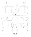
- FIG. 4 is a schematic view illustrating a graded deposition process within the deposition chamber of the deposition machine of FIG. 2.
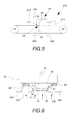
- FIG. 5 is a schematic view of a selective deposition machine for use in the system of FIG. 1 and constructed in accordance with an embodiment of the invention.
- FIG. 6 is a schematic view of an object being selectively coated in the selective deposition machine of FIG. 5.
- FIG. 7 is a schematic view of a selective deposition machine for use in the system of FIG. 1 and constructed in accordance with an embodiment of the invention.
- FIG. 8 is a schematic view of an object being selectively coated in the selective deposition machine of FIG. 7.
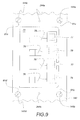
- FIG. 9 is a schematic view of a shadow mask or web for use in the selective deposition machines of FIGS. 5 or 7 and constructed in accordance with an embodiment of the invention.
- Referring to FIG. 1, there is shown a fabrication and
selective coating system 5 that includes asubstrate deposition machine 10, afabrication assembly 110, and aselective coating assembly 210. Arrows are provided to indicate the likely pathway for the coating and fabrication of objects, such as, for example, electronic devices. Examples of electronic devices include liquid crystal displays (LCDs); thin-film transistors (TFTs) and TFT arrays using organic, solution-processible inorganic materials; photovoltaic cells; integrated circuits; electrochromic devices; electrophoretic devices; sensors; energy storage devices, including batteries; electric luminescence devices, including OLEDs; components of medical diagnostic systems; and, any opto-electronic devices that need barrier protection. Specifically, a flexible or inflexible substrate is coated in thesubstrate deposition machine 10. The coated substrate is transferred to thefabrication assembly 110, in which an electronic device is assembled onto the coated substrate. Finally, in theselective coating assembly 210, the electronic device is selectively coated. Thesubstrate deposition machine 10 may utilize a roll-to-roll mechanism or an in-process mechanism to transfer substrates through the machine. - With specific reference to FIGS. 1-4, the
deposition machine 10 is illustrated including afirst spool chamber 12, adeposition chamber 18, and asecond spool chamber 30. Thedeposition machine 10 may be configured to produce a graded-composition coating, for example a graded-composition diffusion-barrier coating, on a substrate. Thefirst spool chamber 12 includes afirst spool 14 about which aweb 40 is wound. Theweb 40 extends through thedeposition chamber 18 and into thesecond spool chamber 30 to asecond spool 32. In one exemplary embodiment, thefirst spool 14 is an unwinding spool and thesecond spool 32 is a winding spool. Theweb 40 may serve as a transportation device transporting a substrate through thedeposition chamber 18; alternatively, theweb 40 may serve as the substrate. Examples of substrates upon which deposition may occur include flexible substrates, such as, for example, films or sheets formed of plastic or metal, and inflexible substrates, such as, for example, blocks or plates formed of glass, metal or plastic. - Substrate materials that may benefit from having a graded-composition diffusion-barrier coating include organic polymeric materials, such as: polyethyleneterephthalate ("PET"); polyacrylates; polycarbonate; silicone; epoxy resins; siliconefunctionalized epoxy resins; polyester, such as Mylar® (made by E.I. du Pont de Nemours & Co.); polyimide, such as Kapton® H or Kapton® E (made by du Pont), Apical® AV (made by Kanegafugi Chemical Industry Company), Upilex® (made by UBE Industries, Ltd.); polyethersulfones ("PES," made by Sumitomo); polyetherimide such as Ultem® (made by General Electric Company); and polyethylene naphthalene ("PEN").
- Suitable coating compositions for the substrates organic, inorganic, or combinations thereof. These materials are typically reaction or recombination products of reacting plasma species and are deposited onto the substrate surface. Organic coating materials typically comprise carbon, hydrogen, oxygen, and optionally other minor elements, such as sulfur, nitrogen, silicon, etc., depending on the types of reactants. Suitable reactants that result in organic compositions in the coating are straight or branched alkanes, alkenes, alkynes, alcohols, aldehydes, ethers, alkylene oxides, aromatics, etc., having up to 15 carbon atoms. Inorganic and ceramic coating materials typically comprise oxide; nitride; carbide; boride; or combinations thereof of elements of Groups IIA, IIIA, IVA, VA, VIA, VIIA, IB, and IIB; metals of Groups IIIB, IVB, and VB; and rare-earth metals. For example, silicon carbide can be deposited onto a substrate by recombination of plasmas generated from silane (SiH4) and an organic material, such as methane or xylene. Silicon oxycarbide can be deposited from plasmas generated from silane, methane, and oxygen or silane and propylene oxide. Silicon oxycarbide also can be deposited from plasmas generated from organosilicone precursors, such as tetraethoxysilane (TEOS), hexamethyldisiloxane (HMDSO), hexamethyldisilazane (HMDSN), or octamethylcyclotetrasiloxane (D4). Silicon nitride can be deposited from plasmas generated from silane and ammonia. Aluminum oxycarbonitride can be deposited from a plasma generated from a mixture of aluminum tartrate and ammonia. Other combinations of reactants may be chosen to obtain a desired coating composition. The choice of the particular reactants is within the skills of the artisans. A graded composition of the coating is obtained by changing the compositions of the reactants fed into the reactor chamber during the deposition of reaction products to form the coating.
- Coating thickness is typically in the range from about 10 nm to about 10000 nm, preferably from about 10 nm to about 1000 nm, and more preferably from about 10 nm to about 200 nm. It may be desired to choose a coating thickness that does not impede the transmission of light through the substrate, such as a reduction in light transmission being less than about 20 percent, preferably less than about 10 percent, and more preferably less than about 5 percent. The coating may be formed by one of many deposition techniques, such as plasma-enhanced chemical-vapor deposition ("PECVD"), radio-frequency plasma-enhanced chemical-vapor deposition ("RFPECVD"), expanding thermal-plasma chemical-vapor deposition ("ETPCVD"), sputtering including reactive sputtering, electron-cyclotron-resonance plasma-enhanced chemical-vapor deposition ("ECRPECVD"), inductively coupled plasma-enhanced chemical-vapor deposition ("ICPECVD"), or combinations thereof. Alternately, the coating may be formed through an evaporative process, a sputtering process, and an atomic layer deposition process.
- Further discussion of suitable substrate materials, suitable coating compositions and suitable coating thicknesses is found in co-pending
U.S. and currently owned by the assignee of the present patent application, the entirety of which is incorporated herein by reference.patent application number 10/065018, filed September 11, 2002 - An
outlet 16 extends from thefirst chamber 12 to the deposition chamber 18 (FIG. 2). Anoutlet 28 extends from thedeposition chamber 18 to thesecond chamber 32. Thedeposition chamber 18 includes at least a first chamber area orsubchamber 20a and a second chamber area orsubchamber 20b. The twochamber areas baffle 24. Thebaffle 24 has anopening 26. Theopening 26 may be adjustable to control the rate of migration of deposition material through theopening 26. Thedeposition chamber 18 may be under vacuum. Further, for mechanical efficiency, the first andsecond chambers - Each chamber area includes a deposition assembly, a deposition material outlet and a gas inlet. Specifically, and with reference to FIG. 3, the
first chamber area 20a includes agas inlet 50 extending to adeposition assembly 52. Thegas inlet 50 receives a gaseous material which is transported to thedeposition assembly 52 to create a deposition mist for the substrate being transported by theweb 40. Any excess deposition material may be removed from thefirst chamber area 20a through thedeposition material outlet 54. Thesecond chamber area 20b includes agas inlet 60 extending to adeposition assembly 62. Thegas inlet 60 receives a gaseous material which is transported to thedeposition assembly 62 to create a deposition mist for the substrate being transported by theweb 40. Any excess deposition material may be removed from thesecond chamber area 20b through thedeposition material outlet 64. Theoutlets deposition chamber area outlets deposition chamber areas outlet deposition chamber areas - To form a graded-composition coating on the substrate, it is envisioned that the material received by the
first deposition assembly 52 has a different composition than the material received by thesecond deposition assembly 62. For example, one material may be an organic material, while a second material is an inorganic material or combinations of inorganic and organic. - With specific reference to FIG. 4, a function of the
baffle 24 and theopening 26 is further described. Thebaffle 24 is adjusted to create anopening 26 of sufficient size and configuration to allow a certain amount of migration of deposition material to occur from one chamber area to another chamber area. As schematically illustrated in FIG. 4, a gaseous material deposited by thefirst deposition assembly 52 results in acoating portion 51 having a relatively high composition of the first gaseous material. Also, a gaseous material deposited by thesecond deposition assembly 62 results in acoating portion 61 having a relatively high composition of the second gaseous material. - Excess deposition material is evacuated from each of the
chamber areas respective outlets chamber areas outlets deposition chamber areas mix area 66 is formed immediately adjacent to thebaffle 24. There is no localized pressure differential in themix area 66. In thismix area 66, deposition material from thesecond chamber area 20b is equally likely to migrate into thefirst chamber area 20a as remain in thesecond chamber area 20b and deposition material from thefirst chamber area 20a is equally likely to migrate into thesecond chamber area 20b as remain in thefirst chamber area 20a. In thismix area 66, the relative compositions of the deposition materials begin to change. For example, the composition of thecoating portion 51 begins to drop in themix area 66, while the composition of thecoating portion 61 begins to increase as an object moves from thefirst chamber area 20a through themix area 66 and into thesecond chamber area 20b. The pressures indeposition chamber areas mix area 66 to various locations within thedeposition chamber 18. For example, pressure indeposition chamber area 20a may be set lower than that ofdeposition chamber area 20b. Thus, deposition material from bothdeposition chamber area 20a anddeposition chamber area 20b is more likely to migrate tooutlet 54 and therefore mixarea 66 will move intodeposition chamber 20a. By engineeringopening 26, pressures indeposition chamber areas deposition assemblies deposition assemblies outlets deposition chamber areas - According to an exemplary embodiment, the substrate to be coated is unwound from the
first spool 14. As theweb 40 travels through thedeposition chamber 18, the first andsecond deposition assemblies - Further discussion of the coating of substrates is found in co-pending
U.S. patent application number 11/315248, filed December 23, 2005 - It should be appreciated that the
web 40 can be wound through thedeposition chamber 18 toward thesecond spool 32 and then wound back through thedeposition chamber 18 toward thefirst spool 14 to obtain a coating having more than three graded zones. Alternatively, and with specific reference to FIG. 4, it should be appreciated that numerous chamber areas or subchambers may be positioned side by side through which theweb 40 may be transported. It should be further appreciated that such asubstrate deposition machine 10 may be modularly assembled. For example, subchambers may be added to the deposition machine or removed from the deposition machine depending upon the particular application. By being able to add and remove subchambers to the entire substrate coating process, flexibility in applicability for thesubstrate deposition machine 10 is enhanced. Additionally, it should be appreciated that instead of a roll-to-roll design as illustrated in FIG. 2, thesubstrate deposition machine 10 may be designed as an "inline" coating machine where theweb 40 is not unwound from one spool and wound onto another spool, but instead continually loops between a pair of spools. - After coating, the substrate is then fed into the
fabrication assembly 110, where electronic devices are fabricated on the coated substrates. In thefabrication assembly 110, an electronic device 70 (FIG. 5) is fabricated. Some of the fabrication steps may be performed under vacuum or inert atmosphere, while other fabrication steps may be performed under atmospheric conditions. It should be appreciated that certain mechanical and chemical properties are desirable for substrates to be used for mounting electronic devices such as organic light-emitting devices (OLEDs), organic photovoltaic devices, thin-film transistors (TFTs) and TFT arrays using organic and solution-processible inorganic materials, and other more complicated circuits. Mechanical flexibility of the substrate is of importance for roll-to-roll processing, as described herein. Similar flexibility is also required for various end-use applications, such as, for example, "roll-up" displays. For "inline" fabrication, flexibility of the substrate is not as important. Chemical resistance is also important for substrate compatibility with the various solvents and chemicals used in the organic electronic device fabrication steps. Further discussion of important mechanical and chemical properties for suitable substrates is found in M. Yan, et al., "A Transparent, High Barrier, and High Heat Substrate for Organic Electronics," IEEE, V. 93, N. 8, August 2005, p. 1468-1477, the entirety of which is incorporated herein by reference. - The compositionally graded ultra-high barrier (UHB) coating described above can effectively stop defects from propagating through the coating thickness. In such a barrier structure, organic materials effectively decouple defects growing in the thickness direction but, instead of having a sharp interface between inorganic and organic materials, there are "transitional" zones where the coating composition varies continuously from inorganic to organic and vice versa. These "transitional" zones bridge inorganic and organic materials, which should result in a single layer structure with improved mechanical stability and stress relaxation relative to that of multilayer barrier structures.
- Such a graded diffusion barrier coating also may be used to protect objects that are sensitive to environmental reactive species such as oxygen and water vapor. Such objects include, but are not limited to, organic light emitting diodes (OLEDs), liquid crystal devices (LCDs), photovoltaic cells, electrochromic devices, electrophoretic devices, and the like.
- Referring now to FIG. 5, the
selective coating assembly 210 is shown. Fabricatedelectronic devices 70 may be moved from the fabrication assembly to the selective coating assembly through the use of a web or through the use of a mechanism for moving individualelectronic devices 70. Examples of such a mechanism include a vacuum chuck, a claw, or adhesive tape. - The
selective coating assembly 210 includes adeposition chamber 18, afirst transition chamber 212, asecond transition chamber 214 and aweb 140. Theweb 140 continually loops between afirst spool 14 and asecond spool 32. Thefirst transition chamber 212 provides a transition between atmospheric conditions and vacuum or inert gas conditions. Thesecond transition chamber 214 provides a transition between vacuum or inert gas conditions of thedeposition chamber 18 and atmospheric conditions. Theweb 140 as used in theselective coating assembly 210 of FIG. 5 differs from theweb 40 as used in thesubstrate deposition machine 10 of FIG. 2 in that theweb 140 includes open spaces 142 (FIG. 9). - FIG. 6 illustrates an electronic device mounted on a substrate. The coating of the electronic device is a similar process to the coating of the substrate described with reference to FIG. 2. The
electronic device 70 illustrated in FIG. 6 has been mounted on asubstrate 72 that has been coated with a graded barrier coating in thesubstrate deposition machine 10. Thesubstrate 72 may be flexible, as in a film or thin sheet of plastic or metal, or inflexible, as in a block of glass, plastic or metal. The illustratedelectronic device 70, fabricated in thefabrication assembly 110, includes anOLED 74, ananode 76, and acathode 78. A positiveelectric contact 77 extends from theanode 76 and a negativeelectric contact 79 extends from thecathode 78. It is generally desirable to coat all the portions of theelectronic device 70, with the exception of theelectric contacts electronic device 70 from reactive gaseous species such as moisture and oxygen, and/or from physical or chemical attack. - Specifically, with reference to FIGS. 6 and 9, a
coating 82 is deposited on theelectronic device 70 except over theelectric contacts coating 82 is delivered in the direction of the arrows A. Theelectronic device 70 is placed on theweb 140 in such a way as to allow theopenings 142 to be positioned to allow coating of the portions of theelectronic device 70 that are to be coated and to inhibit coating of the portions of theelectronic device 70 that are not to be coated, namely theelectric contacts electronic device 70 on theweb 140 may be accomplished through the use of reference pins 80 on theelectronic device 70 and reference markers, such as reference slots 244a, 244b, on theweb 140. Only onereference pin 80 is shown in FIG. 6 for ease of illustration, although it should be appreciated that more than onereference pin 80 may be used to properly register theelectronic device 70 with theweb 140. Further, although the reference slots 244a, 244b are shown generally along a midline of theweb 140, it should be appreciated that the reference slots 244a, 244b and the reference pins 80 may be located in any locations suitable for properly registering theelectronic device 70 with theweb 140. - Alternatively, the
electronic device 70 may be registered with theweb 140 through the use reference markers utilizing autocalibration techniques. For example, theweb 140 may include autocalibration markers 144a-d that are used in conjunction with complementary markers 81 a-d on theelectronic device 70. The concept is to site theelectronic device 70 on theweb 140 so that each complementary marker 81 a-d on theelectronic device 70 is sited within a respective autocalibration marker 144a-d on theweb 140. - FIG. 7 illustrates an alternative
selective deposition assembly 310. Theselective deposition assembly 310 includes aweb 40 for transporting theelectronic devices 70 andweb 240 that includes openings in a similar fashion as theweb 140. Theelectronic devices 70 can be built onweb 40 beforehand, such that theweb 40 acts as a substrate for theelectronic devices 70, or can be affixed to theweb 40 with an adhesive 90. Theweb 240 serves as a shadow mask to inhibit coating certain portions of theelectronic devices 70, namely theelectric contacts web 240 can be appropriately registered relative to theelectronic devices 70 by altering the velocity of theweb 240 relative to the velocity of theweb 40. - It should be appreciated that the coating on the
electronic devices 70 may be similar to the graded barrier coating used on thesubstrates 72 as described with reference to FIG. 2. Alternatively, the coating on theelectronic devices 70 may be a hard coating designed to protect theelectronic devices 70 from ultraviolet radiation or from physical or chemical attack, such as scratches and abrasion. Such suitable hard coatings may include, for example, coating compositions that include at least one resin. The resin can be an epoxy-based resin. For example, the resin can be a cycloaliphatic resin. The resin can also be an acrylic-based resin. Some epoxies may impart increased surface durability. A siloxane portion of certain diepoxies may be easily adjusted in length and branching to optimize desired properties. The hard coating composition may further include at least one flexibilizing agent, adhesive agent, surfactant or catalyst and combinations thereof. In still another aspect, the hard coating composition may be cured. The curing may be radiation curing, such as ultraviolet curing, or thermal curing and combinations thereof. Other curing mechanisms can also be employed in place of UV curing, including anhydride or amine curing. Additives can be incorporated into the leveling layer to tailor its properties. For example, a UV catalyst may be added to the layer composition. In another example, UV absorbers can be added to protect underlying UV sensitive layers. Siloxane additives can be included to make the leveling layer more scratch resistant. Antioxidant chemicals such as Irganox®, manufactured by the Geigy Chemical Corporation, hinder amine complexes and can also be added to prevent yellowing of the coating and underlying substrate. Further discussion of suitable hard coating materials, suitable coating compositions and suitable coating thickness may be found in US patent publication numberUS 2006/0001040 . - The selectively coated
electronic devices 70 may be removed from the selective coating assembly through the use of theweb electronic devices 70. Examples of such a mechanism include a vacuum chuck, a claw, or adhesive tape. - While the invention has been described in detail in connection with only a limited number of embodiments, it should be readily understood that the invention is not limited to such disclosed embodiments. Rather, the invention can be modified to incorporate any number of variations, alterations, substitutions or equivalent arrangements not heretofore described, but which are commensurate with the spirit and scope of the invention. For example, although the
electronic device 70 has been described with reference to an OLED device, it should be appreciated that any suitable electronic device may be used that requires encapsulation or coating on some but not all portions. Additionally, while various embodiments of the invention have been described, it is to be understood that aspects of the invention may include only some of the described embodiments. Accordingly, the invention is not to be seen as limited by the foregoing description, but is only limited by the scope of the appended claims. - For completeness, various aspects of the invention are now set out in the following numbered clauses:
- 1. A selective deposition assembly, comprising:
- a deposition chamber having at least one gas inlet; and
- a web extending through said deposition chamber and positioned between said at least one gas inlet and an object, said web including openings to enable coating of a deposition material upon selected portions of the object.
- 2. The selective deposition assembly of clause 1, wherein said web extends between first and second spools to allow continual movement of said web through said deposition chamber.
- 3. The selective deposition assembly of clause 1, comprising one or more reference markers.
- 4. The selective deposition assembly of clause 3, wherein said one or more reference markers comprises reference slots.
- 5. The selective deposition assembly of clause 3, wherein said one or more reference markers comprises autocalibration markers.
- 6. The selective deposition assembly of clause 1, comprising a second web upon which the object is affixed.
- 7. The selective deposition assembly of clause 1, wherein said deposition chamber comprises a first chamber area separated from a second chamber area by a baffle having an opening.
- 8. The selective deposition assembly of clause 1, wherein said deposition chamber is adapted to deposit a graded barrier coating on the object.
- 9. The selective deposition assembly of clause 1, wherein said deposition chamber is adapted to deposit a hard coating on the object.
- 10. The selective deposition assembly of clause 1, wherein the object comprises an electronic device.
- 11. The selective deposition assembly of
clause 10, wherein the electronic device comprises one selected from the group consisting of liquid crystal displays, thin-film transistors, thin-film transistor arrays using organic, solution-processible inorganic materials, photovoltaic cells, integrated circuits, electrochromic devices, electrophoretic devices, sensors, energy storage devices, electric luminescence devices, components of medical diagnostic systems, and opto-electronic devices. - 12. A fabrication and selective coating system, comprising:
- a substrate deposition machine to enable coating of a substrate;
- a fabrication assembly to enable fabrication of an object on the substrate; and
- a selective coating assembly to enable coating of selective portions of the object.
- 13. The fabrication and selective coating system of
clause 12, wherein the selective coating assembly comprises:- a deposition chamber having at least one gas inlet; and
- a web extending through said deposition chamber and positioned between said at least one gas inlet and the object, wherein said web has openings to enable coating of a deposition material upon selected portions of the object.
- 14. The fabrication and selective coating system of clause 13, wherein said web comprises one or more reference markers for registering the object with said web.
- 15. The fabrication and selective coating system of
clause 12, wherein said selective coating assembly comprises a first transition chamber positioned between said fabrication assembly and said selective coating assembly and a second transition chamber positioned after said selective coating assembly. - 16. The fabrication and selective coating system of
clause 12, comprising a mechanism for removing the object from said selective coating assembly. - 17. The fabrication and selective coating system of
clause 16, wherein said mechanism comprises one from the group consisting of vacuum chuck, claw, and tape. - 18. The fabrication and selective coating system of
clause 12, wherein said deposition chamber is adapted to form a graded barrier coating on the object - 19. The fabrication and selective coating system of
clause 12, wherein said deposition chamber is adapted to form a hard coating on the object. - 20. The fabrication and selective coating system of
clause 12, wherein the object comprises an electronic device. - 21. A method for inhibiting coating selective portions of an object, comprising:
- transporting the object through a deposition chamber;
- providing a shadow mask opposite the object for inhibiting coating of selective portions of the object; and
- providing a deposition material to serve as a coating.
- 22. The method of clause 21, wherein said transporting comprises providing a web upon which the object is placed.
- 23. The method of clause 22, wherein said providing a shadow mask comprises providing a web that includes openings to allow the deposition material to coat selective portions of the object.
- 24. The method of clause 23, wherein the web used for said transporting includes the openings.
- 25. The method of clause 23, comprising registering the object relative to the web to ensure the selective portions of the object remain uncoated.
- 26. The method of clause 25, wherein said registering comprises providing reference markers on the object and the web serving as the shadow mask.
- 27. The method of
clause 26, wherein said providing reference markers comprises providing reference pins on the object and reference slots on the web serving as the shadow mask. - 28. The method of
clause 26, wherein said providing reference markers comprises providing autocalibration markers on the web serving as the shadow mask and complementary markers on the object. - 29. The method of clause 21, wherein said providing a deposition material comprises producing a graded barrier coating.
- 30. The method of clause 21, wherein said providing a deposition material comprises producing a hard coating.
- 31. The method of clause 21, wherein said providing a deposition material comprises plasma-enhanced chemical-vapor deposition, radio-frequency plasma-enhanced chemical-vapor deposition, expanding thermal-plasma chemical-vapor deposition, sputtering including reactive sputtering, electron-cyclotron-resonance plasma-enhanced chemical-vapor deposition, inductively coupled plasma-enhanced chemical-vapor deposition, evaporation, atomic layer deposition, or combinations thereof.
Claims (11)
- A selective deposition assembly (210), comprising:a deposition chamber (18) having at least one gas inlet (50); anda web (140) extending through said deposition chamber and positioned between said at least one gas inlet and an object (70), said web including openings (142) to enable coating of a deposition material upon selected portions of the object.
- The selective deposition assembly of claim 1, wherein said web extends between first and second spools (14, 32) to allow continual movement of said web through said deposition chamber.
- The selective deposition assembly of claim 1 or claim 2, comprising one or more reference markers (144a-d or 244a,b).
- The selective deposition assembly of claim 3, wherein said one or more reference markers comprises reference slots (244a,b).
- The selective deposition assembly of claim 3, wherein said one or more reference markers comprises autocalibration markers (144a-d).
- The selective deposition assembly of any preceding claim, comprising a second web (40) upon which the object is affixed.
- The selective deposition assembly of any preceding claim, wherein said deposition chamber comprises a first chamber area (20a) separated from a second chamber area (20b) by a baffle (24) having an opening (26).
- The selective deposition assembly of any preceding claim, wherein said deposition chamber is adapted to deposit a graded barrier coating (82) on the object.
- The selective deposition assembly of any preceding claim, wherein said deposition chamber is adapted to deposit a hard coating (82) on the object.
- The selective deposition assembly of any preceding claim, wherein the object comprises an electronic device.
- The selective deposition assembly of claim 10, wherein the electronic device comprises one selected from the group consisting of liquid crystal displays, thin-film transistors, thin-film transistor arrays using organic, solution-processible inorganic materials, photovoltaic cells, integrated circuits, electrochromic devices, electrophoretic devices, sensors, energy storage devices, electric luminescence devices, components of medical diagnostic systems, and opto-electronic devices.
Applications Claiming Priority (1)
| Application Number | Priority Date | Filing Date | Title |
|---|---|---|---|
| US11/585,295 US7976899B2 (en) | 2006-10-23 | 2006-10-23 | Methods for selective deposition of graded materials on continuously fed objects |
Publications (1)
| Publication Number | Publication Date |
|---|---|
| EP1918412A1 true EP1918412A1 (en) | 2008-05-07 |
Family
ID=38956403
Family Applications (1)
| Application Number | Title | Priority Date | Filing Date |
|---|---|---|---|
| EP07115356A Ceased EP1918412A1 (en) | 2006-10-23 | 2007-08-30 | Apparatus for selective deposition of graded coatings |
Country Status (2)
| Country | Link |
|---|---|
| US (1) | US7976899B2 (en) |
| EP (1) | EP1918412A1 (en) |
Cited By (17)
| Publication number | Priority date | Publication date | Assignee | Title |
|---|---|---|---|---|
| CN102686769A (en) * | 2010-01-04 | 2012-09-19 | 德国罗特·劳股份有限公司 | Method for depositing multi-layered layers and/or gradient layers |
| CN104364707A (en) * | 2012-05-02 | 2015-02-18 | 唯景公司 | Electrochromic Devices |
| US9671664B2 (en) | 2010-04-30 | 2017-06-06 | View, Inc. | Electrochromic devices |
| US9720298B2 (en) | 2010-04-30 | 2017-08-01 | View, Inc. | Electrochromic devices |
| CN107015411A (en) * | 2010-04-30 | 2017-08-04 | 唯景公司 | The method and apparatus of electrochromic device and the manufacture device |
| US9759975B2 (en) | 2010-04-30 | 2017-09-12 | View, Inc. | Electrochromic devices |
| US10054833B2 (en) | 2009-03-31 | 2018-08-21 | View, Inc. | Fabrication of low defectivity electrochromic devices |
| US10156762B2 (en) | 2009-03-31 | 2018-12-18 | View, Inc. | Counter electrode for electrochromic devices |
| US10228601B2 (en) | 2014-11-26 | 2019-03-12 | View, Inc. | Counter electrode for electrochromic devices |
| US10261381B2 (en) | 2009-03-31 | 2019-04-16 | View, Inc. | Fabrication of low defectivity electrochromic devices |
| US10345671B2 (en) | 2014-09-05 | 2019-07-09 | View, Inc. | Counter electrode for electrochromic devices |
| US10591795B2 (en) | 2009-03-31 | 2020-03-17 | View, Inc. | Counter electrode for electrochromic devices |
| US10852613B2 (en) | 2009-03-31 | 2020-12-01 | View, Inc. | Counter electrode material for electrochromic devices |
| US11187954B2 (en) | 2009-03-31 | 2021-11-30 | View, Inc. | Electrochromic cathode materials |
| US11891327B2 (en) | 2014-05-02 | 2024-02-06 | View, Inc. | Fabrication of low defectivity electrochromic devices |
| US12043890B2 (en) | 2009-03-31 | 2024-07-23 | View, Inc. | Electrochromic devices |
| US12353109B2 (en) | 2009-12-22 | 2025-07-08 | View Operating Corporation | Electrochromic cathode materials |
Families Citing this family (13)
| Publication number | Priority date | Publication date | Assignee | Title |
|---|---|---|---|---|
| EP2000008B1 (en) | 2006-03-26 | 2011-04-27 | Lotus Applied Technology, Llc | Atomic layer deposition system and method for coating flexible substrates |
| WO2008016836A2 (en) | 2006-07-29 | 2008-02-07 | Lotus Applied Technology, Llc | Radical-enhanced atomic layer deposition system and method |
| US20090291035A1 (en) * | 2008-05-23 | 2009-11-26 | Michael Colin Begg | Vacuum chamber |
| FI123170B (en) * | 2009-05-26 | 2012-11-30 | Beneq Oy | Device for treating substrates and mounting plate for substrates |
| US20110065282A1 (en) * | 2009-09-11 | 2011-03-17 | General Electric Company | Apparatus and methods to form a patterned coating on an oled substrate |
| US8637117B2 (en) | 2009-10-14 | 2014-01-28 | Lotus Applied Technology, Llc | Inhibiting excess precursor transport between separate precursor zones in an atomic layer deposition system |
| US8637123B2 (en) * | 2009-12-29 | 2014-01-28 | Lotus Applied Technology, Llc | Oxygen radical generation for radical-enhanced thin film deposition |
| US9297076B2 (en) | 2010-07-23 | 2016-03-29 | Lotus Applied Technology, Llc | Substrate transport mechanism contacting a single side of a flexible web substrate for roll-to-roll thin film deposition |
| TWI459563B (en) * | 2011-04-01 | 2014-11-01 | Chunghwa Picture Tubes Ltd | Transistor array substrate |
| US8884476B2 (en) * | 2011-09-23 | 2014-11-11 | General Electric Company | Hybrid dielectric film for high temperature application |
| US9731456B2 (en) | 2013-03-14 | 2017-08-15 | Sabic Global Technologies B.V. | Method of manufacturing a functionally graded article |
| US9435028B2 (en) | 2013-05-06 | 2016-09-06 | Lotus Applied Technology, Llc | Plasma generation for thin film deposition on flexible substrates |
| JP2017182062A (en) * | 2016-03-25 | 2017-10-05 | 日東電工株式会社 | Manufacturing method of light control film |
Citations (4)
| Publication number | Priority date | Publication date | Assignee | Title |
|---|---|---|---|---|
| US4416217A (en) * | 1981-07-31 | 1983-11-22 | Ulvac Seimaku Kabushiki Kaisha | Apparatus for forming an inhomogeneous optical layer |
| JPH0578818A (en) * | 1991-09-19 | 1993-03-30 | Hitachi Cable Ltd | Formation of partial film |
| US20030152691A1 (en) * | 2002-02-14 | 2003-08-14 | 3M Innovative Properties Company | In-line deposition processes for circuit fabrication |
| US20060001040A1 (en) | 2004-06-30 | 2006-01-05 | General Electric Company | High integrity protective coatings |
Family Cites Families (7)
| Publication number | Priority date | Publication date | Assignee | Title |
|---|---|---|---|---|
| GB8408023D0 (en) * | 1984-03-28 | 1984-05-10 | Gen Eng Radcliffe Ltd | Vacuum coating apparatus |
| US20030192584A1 (en) * | 2002-01-25 | 2003-10-16 | Konarka Technologies, Inc. | Flexible photovoltaic cells and modules formed using foils |
| US20030059526A1 (en) * | 2001-09-12 | 2003-03-27 | Benson Martin H. | Apparatus and method for the design and manufacture of patterned multilayer thin films and devices on fibrous or ribbon-like substrates |
| TW574538B (en) * | 2002-04-24 | 2004-02-01 | Sipix Imaging Inc | Compositions and processes for format flexible roll-to-roll manufacturing of electrophoretic displays |
| US20060024442A1 (en) * | 2003-05-19 | 2006-02-02 | Ovshinsky Stanford R | Deposition methods for the formation of polycrystalline materials on mobile substrates |
| US7309644B2 (en) * | 2004-11-29 | 2007-12-18 | University Of Maryland, College Park | System and method of fabrication and application of thin-films with continuously graded or discrete physical property parameters to functionally broadband monolithic microelectronic optoelectronic/sensor/actuator device arrays |
| US20070148346A1 (en) * | 2005-12-23 | 2007-06-28 | General Electric Company | Systems and methods for deposition of graded materials on continuously fed objects |
-
2006
- 2006-10-23 US US11/585,295 patent/US7976899B2/en active Active
-
2007
- 2007-08-30 EP EP07115356A patent/EP1918412A1/en not_active Ceased
Patent Citations (4)
| Publication number | Priority date | Publication date | Assignee | Title |
|---|---|---|---|---|
| US4416217A (en) * | 1981-07-31 | 1983-11-22 | Ulvac Seimaku Kabushiki Kaisha | Apparatus for forming an inhomogeneous optical layer |
| JPH0578818A (en) * | 1991-09-19 | 1993-03-30 | Hitachi Cable Ltd | Formation of partial film |
| US20030152691A1 (en) * | 2002-02-14 | 2003-08-14 | 3M Innovative Properties Company | In-line deposition processes for circuit fabrication |
| US20060001040A1 (en) | 2004-06-30 | 2006-01-05 | General Electric Company | High integrity protective coatings |
Cited By (46)
| Publication number | Priority date | Publication date | Assignee | Title |
|---|---|---|---|---|
| US11898233B2 (en) | 2009-03-31 | 2024-02-13 | View, Inc. | Electrochromic devices |
| US11409177B2 (en) | 2009-03-31 | 2022-08-09 | View, Inc. | Counter electrode for electrochromic devices |
| US11370699B2 (en) | 2009-03-31 | 2022-06-28 | View, Inc. | Counter electrode for electrochromic devices |
| US10852613B2 (en) | 2009-03-31 | 2020-12-01 | View, Inc. | Counter electrode material for electrochromic devices |
| US10690987B2 (en) | 2009-03-31 | 2020-06-23 | View, Inc. | Counter electrode for electrochromic devices |
| US12242163B2 (en) | 2009-03-31 | 2025-03-04 | View, Inc. | Fabrication of low defectivity electrochromic devices |
| US12209048B2 (en) | 2009-03-31 | 2025-01-28 | View, Inc. | Counter electrode for electrochromic devices |
| US12043890B2 (en) | 2009-03-31 | 2024-07-23 | View, Inc. | Electrochromic devices |
| US11966140B2 (en) | 2009-03-31 | 2024-04-23 | View, Inc. | Counter electrode for electrochromic devices |
| US10054833B2 (en) | 2009-03-31 | 2018-08-21 | View, Inc. | Fabrication of low defectivity electrochromic devices |
| US11947232B2 (en) | 2009-03-31 | 2024-04-02 | View, Inc. | Fabrication of low defectivity electrochromic devices |
| US10156762B2 (en) | 2009-03-31 | 2018-12-18 | View, Inc. | Counter electrode for electrochromic devices |
| US12443085B2 (en) | 2009-03-31 | 2025-10-14 | View Operating Corporation | Counter electrode for electrochromic devices |
| US11187954B2 (en) | 2009-03-31 | 2021-11-30 | View, Inc. | Electrochromic cathode materials |
| US10591797B2 (en) | 2009-03-31 | 2020-03-17 | View, Inc. | Electrochromic devices |
| US10261381B2 (en) | 2009-03-31 | 2019-04-16 | View, Inc. | Fabrication of low defectivity electrochromic devices |
| US11635665B2 (en) | 2009-03-31 | 2023-04-25 | View, Inc. | Counter electrode material for electrochromic devices |
| US11525181B2 (en) | 2009-03-31 | 2022-12-13 | View, Inc. | Electrochromic devices |
| US10254615B2 (en) | 2009-03-31 | 2019-04-09 | View, Inc. | Fabrication of low defectivity electrochromic devices |
| US10591795B2 (en) | 2009-03-31 | 2020-03-17 | View, Inc. | Counter electrode for electrochromic devices |
| US11440838B2 (en) | 2009-03-31 | 2022-09-13 | View, Inc. | Fabrication of low defectivity electrochromic devices |
| US10663830B2 (en) | 2009-03-31 | 2020-05-26 | View, Inc. | Fabrication of low defectivity electrochromic devices |
| US12353109B2 (en) | 2009-12-22 | 2025-07-08 | View Operating Corporation | Electrochromic cathode materials |
| US12366784B2 (en) | 2009-12-22 | 2025-07-22 | View Operating Corporation | Electrochromic cathode materials |
| CN102686769A (en) * | 2010-01-04 | 2012-09-19 | 德国罗特·劳股份有限公司 | Method for depositing multi-layered layers and/or gradient layers |
| CN102686769B (en) * | 2010-01-04 | 2015-11-25 | 德国罗特·劳股份有限公司 | For the method for deposit multilayer formula layer and/or gradient layer |
| US11592722B2 (en) | 2010-04-30 | 2023-02-28 | View, Inc. | Electrochromic devices |
| US10185197B2 (en) | 2010-04-30 | 2019-01-22 | View, Inc. | Electrochromic devices |
| US10996533B2 (en) | 2010-04-30 | 2021-05-04 | View, Inc. | Electrochromic devices |
| US9671664B2 (en) | 2010-04-30 | 2017-06-06 | View, Inc. | Electrochromic devices |
| US9720298B2 (en) | 2010-04-30 | 2017-08-01 | View, Inc. | Electrochromic devices |
| US10599001B2 (en) | 2010-04-30 | 2020-03-24 | View, Inc. | Electrochromic devices |
| CN107015411A (en) * | 2010-04-30 | 2017-08-04 | 唯景公司 | The method and apparatus of electrochromic device and the manufacture device |
| US9759975B2 (en) | 2010-04-30 | 2017-09-12 | View, Inc. | Electrochromic devices |
| US10088729B2 (en) | 2010-04-30 | 2018-10-02 | View, Inc. | Electrochromic devices |
| CN104364707B (en) * | 2012-05-02 | 2018-03-27 | 唯景公司 | electrochromic device |
| EP2845051A4 (en) * | 2012-05-02 | 2016-05-04 | View Inc | ELECTROCHROME DEVICES |
| CN104364707A (en) * | 2012-05-02 | 2015-02-18 | 唯景公司 | Electrochromic Devices |
| US11891327B2 (en) | 2014-05-02 | 2024-02-06 | View, Inc. | Fabrication of low defectivity electrochromic devices |
| US10345671B2 (en) | 2014-09-05 | 2019-07-09 | View, Inc. | Counter electrode for electrochromic devices |
| US11422426B2 (en) | 2014-09-05 | 2022-08-23 | View, Inc. | Counter electrode for electrochromic devices |
| US10684523B2 (en) | 2014-09-05 | 2020-06-16 | View, Inc. | Counter electrode for electrochromic devices |
| US10228601B2 (en) | 2014-11-26 | 2019-03-12 | View, Inc. | Counter electrode for electrochromic devices |
| US11960188B2 (en) | 2014-11-26 | 2024-04-16 | View, Inc. | Counter electrode for electrochromic devices |
| US11327382B2 (en) | 2014-11-26 | 2022-05-10 | View, Inc. | Counter electrode for electrochromic devices |
| US10585321B2 (en) | 2014-11-26 | 2020-03-10 | View, Inc. | Counter electrode for electrochromic devices |
Also Published As
| Publication number | Publication date |
|---|---|
| US7976899B2 (en) | 2011-07-12 |
| US20080092814A1 (en) | 2008-04-24 |
Similar Documents
| Publication | Publication Date | Title |
|---|---|---|
| US7976899B2 (en) | Methods for selective deposition of graded materials on continuously fed objects | |
| US7074501B2 (en) | Coatings with low permeation of gases and vapors | |
| EP1859496B1 (en) | High integrity protective coating | |
| CN101809188B (en) | Process for forming a thin film sealing layer | |
| CN102433549B (en) | Process of making optical film by atomic layer deposition (ALD) at atmospheric pressure | |
| US8828528B2 (en) | Barrier film and method of manufacturing the same | |
| US20100092781A1 (en) | Roll-To-Roll Plasma Enhanced Chemical Vapor Deposition Method of Barrier Layers Comprising Silicon And Carbon | |
| US20050172897A1 (en) | Barrier layer process and arrangement | |
| EP1930250A2 (en) | Barrier layer, composite article comprising the same, electroactive device, and method | |
| JP6332283B2 (en) | Gas barrier film | |
| CN105390621A (en) | Thin film permeation barrier system for substrates and devices and method of making the same | |
| JPWO2014123201A1 (en) | Gas barrier film and method for producing the same | |
| US10961622B2 (en) | Gas barrier film and method of manufacturing the same | |
| CN101743267B (en) | Multilayer film and its manufacturing method | |
| EP1564825A2 (en) | Composite articles having diffusion barriers and devices incorporating them | |
| US8691371B2 (en) | Barrier coating and method | |
| JP4506365B2 (en) | Barrier film manufacturing method | |
| US20070148346A1 (en) | Systems and methods for deposition of graded materials on continuously fed objects | |
| Chen | Realizing Thin‐Film Encapsulation's Benefits for Large‐Scale OLED Panels | |
| JP4525330B2 (en) | Method for producing conductive gas barrier laminate | |
| JP2016074927A (en) | Film deposition device and film deposition method | |
| JP2017109438A (en) | Gas barrier film and organic el light-emitting element using the same |
Legal Events
| Date | Code | Title | Description |
|---|---|---|---|
| PUAI | Public reference made under article 153(3) epc to a published international application that has entered the european phase |
Free format text: ORIGINAL CODE: 0009012 |
|
| AK | Designated contracting states |
Kind code of ref document: A1 Designated state(s): AT BE BG CH CY CZ DE DK EE ES FI FR GB GR HU IE IS IT LI LT LU LV MC MT NL PL PT RO SE SI SK TR |
|
| AX | Request for extension of the european patent |
Extension state: AL BA HR MK RS |
|
| 17P | Request for examination filed |
Effective date: 20081107 |
|
| AKX | Designation fees paid |
Designated state(s): AT BE BG CH CY CZ DE DK EE ES FI FR GB GR HU IE IS IT LI LT LU LV MC MT NL PL PT RO SE SI SK TR |
|
| 17Q | First examination report despatched |
Effective date: 20090127 |
|
| STAA | Information on the status of an ep patent application or granted ep patent |
Free format text: STATUS: THE APPLICATION HAS BEEN REFUSED |
|
| 18R | Application refused |
Effective date: 20120102 |