EP1916716A2 - Semiconductor device - Google Patents
Semiconductor device Download PDFInfo
- Publication number
- EP1916716A2 EP1916716A2 EP07021118A EP07021118A EP1916716A2 EP 1916716 A2 EP1916716 A2 EP 1916716A2 EP 07021118 A EP07021118 A EP 07021118A EP 07021118 A EP07021118 A EP 07021118A EP 1916716 A2 EP1916716 A2 EP 1916716A2
- Authority
- EP
- European Patent Office
- Prior art keywords
- electrode
- substrate
- bump
- source
- semiconductor
- Prior art date
- Legal status (The legal status is an assumption and is not a legal conclusion. Google has not performed a legal analysis and makes no representation as to the accuracy of the status listed.)
- Granted
Links
Images


Classifications
-
- H—ELECTRICITY
- H10—SEMICONDUCTOR DEVICES; ELECTRIC SOLID-STATE DEVICES NOT OTHERWISE PROVIDED FOR
- H10W—GENERIC PACKAGES, INTERCONNECTIONS, CONNECTORS OR OTHER CONSTRUCTIONAL DETAILS OF DEVICES COVERED BY CLASS H10
- H10W74/00—Encapsulations, e.g. protective coatings
- H10W74/10—Encapsulations, e.g. protective coatings characterised by their shape or disposition
-
- H—ELECTRICITY
- H10—SEMICONDUCTOR DEVICES; ELECTRIC SOLID-STATE DEVICES NOT OTHERWISE PROVIDED FOR
- H10D—INORGANIC ELECTRIC SEMICONDUCTOR DEVICES
- H10D89/00—Aspects of integrated devices not covered by groups H10D84/00 - H10D88/00
- H10D89/10—Integrated device layouts
-
- H—ELECTRICITY
- H10—SEMICONDUCTOR DEVICES; ELECTRIC SOLID-STATE DEVICES NOT OTHERWISE PROVIDED FOR
- H10D—INORGANIC ELECTRIC SEMICONDUCTOR DEVICES
- H10D84/00—Integrated devices formed in or on semiconductor substrates that comprise only semiconducting layers, e.g. on Si wafers or on GaAs-on-Si wafers
- H10D84/80—Integrated devices formed in or on semiconductor substrates that comprise only semiconducting layers, e.g. on Si wafers or on GaAs-on-Si wafers characterised by the integration of at least one component covered by groups H10D12/00 or H10D30/00, e.g. integration of IGFETs
- H10D84/82—Integrated devices formed in or on semiconductor substrates that comprise only semiconducting layers, e.g. on Si wafers or on GaAs-on-Si wafers characterised by the integration of at least one component covered by groups H10D12/00 or H10D30/00, e.g. integration of IGFETs of only field-effect components
- H10D84/83—Integrated devices formed in or on semiconductor substrates that comprise only semiconducting layers, e.g. on Si wafers or on GaAs-on-Si wafers characterised by the integration of at least one component covered by groups H10D12/00 or H10D30/00, e.g. integration of IGFETs of only field-effect components of only insulated-gate FETs [IGFET]
- H10D84/83125—Integrated devices formed in or on semiconductor substrates that comprise only semiconducting layers, e.g. on Si wafers or on GaAs-on-Si wafers characterised by the integration of at least one component covered by groups H10D12/00 or H10D30/00, e.g. integration of IGFETs of only field-effect components of only insulated-gate FETs [IGFET] the IGFETs characterised by having shared source or drain regions
-
- H—ELECTRICITY
- H10—SEMICONDUCTOR DEVICES; ELECTRIC SOLID-STATE DEVICES NOT OTHERWISE PROVIDED FOR
- H10W—GENERIC PACKAGES, INTERCONNECTIONS, CONNECTORS OR OTHER CONSTRUCTIONAL DETAILS OF DEVICES COVERED BY CLASS H10
- H10W72/00—Interconnections or connectors in packages
- H10W72/01—Manufacture or treatment
- H10W72/012—Manufacture or treatment of bump connectors, dummy bumps or thermal bumps
- H10W72/01221—Manufacture or treatment of bump connectors, dummy bumps or thermal bumps using local deposition
- H10W72/01223—Manufacture or treatment of bump connectors, dummy bumps or thermal bumps using local deposition in liquid form, e.g. by dispensing droplets or by screen printing
-
- H—ELECTRICITY
- H10—SEMICONDUCTOR DEVICES; ELECTRIC SOLID-STATE DEVICES NOT OTHERWISE PROVIDED FOR
- H10W—GENERIC PACKAGES, INTERCONNECTIONS, CONNECTORS OR OTHER CONSTRUCTIONAL DETAILS OF DEVICES COVERED BY CLASS H10
- H10W72/00—Interconnections or connectors in packages
- H10W72/01—Manufacture or treatment
- H10W72/019—Manufacture or treatment of bond pads
- H10W72/01931—Manufacture or treatment of bond pads using blanket deposition
- H10W72/01933—Manufacture or treatment of bond pads using blanket deposition in liquid form, e.g. spin coating, spray coating or immersion coating
- H10W72/01935—Manufacture or treatment of bond pads using blanket deposition in liquid form, e.g. spin coating, spray coating or immersion coating by plating, e.g. electroless plating or electroplating
-
- H—ELECTRICITY
- H10—SEMICONDUCTOR DEVICES; ELECTRIC SOLID-STATE DEVICES NOT OTHERWISE PROVIDED FOR
- H10W—GENERIC PACKAGES, INTERCONNECTIONS, CONNECTORS OR OTHER CONSTRUCTIONAL DETAILS OF DEVICES COVERED BY CLASS H10
- H10W72/00—Interconnections or connectors in packages
- H10W72/071—Connecting or disconnecting
- H10W72/072—Connecting or disconnecting of bump connectors
- H10W72/07231—Techniques
- H10W72/07232—Compression bonding, e.g. thermocompression bonding
- H10W72/07233—Ultrasonic bonding, e.g. thermosonic bonding
-
- H—ELECTRICITY
- H10—SEMICONDUCTOR DEVICES; ELECTRIC SOLID-STATE DEVICES NOT OTHERWISE PROVIDED FOR
- H10W—GENERIC PACKAGES, INTERCONNECTIONS, CONNECTORS OR OTHER CONSTRUCTIONAL DETAILS OF DEVICES COVERED BY CLASS H10
- H10W72/00—Interconnections or connectors in packages
- H10W72/071—Connecting or disconnecting
- H10W72/072—Connecting or disconnecting of bump connectors
- H10W72/07231—Techniques
- H10W72/07236—Soldering or alloying
-
- H—ELECTRICITY
- H10—SEMICONDUCTOR DEVICES; ELECTRIC SOLID-STATE DEVICES NOT OTHERWISE PROVIDED FOR
- H10W—GENERIC PACKAGES, INTERCONNECTIONS, CONNECTORS OR OTHER CONSTRUCTIONAL DETAILS OF DEVICES COVERED BY CLASS H10
- H10W72/00—Interconnections or connectors in packages
- H10W72/20—Bump connectors, e.g. solder bumps or copper pillars; Dummy bumps; Thermal bumps
- H10W72/251—Materials
- H10W72/252—Materials comprising solid metals or solid metalloids, e.g. PbSn, Ag or Cu
-
- H—ELECTRICITY
- H10—SEMICONDUCTOR DEVICES; ELECTRIC SOLID-STATE DEVICES NOT OTHERWISE PROVIDED FOR
- H10W—GENERIC PACKAGES, INTERCONNECTIONS, CONNECTORS OR OTHER CONSTRUCTIONAL DETAILS OF DEVICES COVERED BY CLASS H10
- H10W72/00—Interconnections or connectors in packages
- H10W72/20—Bump connectors, e.g. solder bumps or copper pillars; Dummy bumps; Thermal bumps
- H10W72/29—Bond pads specially adapted therefor
-
- H—ELECTRICITY
- H10—SEMICONDUCTOR DEVICES; ELECTRIC SOLID-STATE DEVICES NOT OTHERWISE PROVIDED FOR
- H10W—GENERIC PACKAGES, INTERCONNECTIONS, CONNECTORS OR OTHER CONSTRUCTIONAL DETAILS OF DEVICES COVERED BY CLASS H10
- H10W72/00—Interconnections or connectors in packages
- H10W72/90—Bond pads, in general
- H10W72/921—Structures or relative sizes of bond pads
- H10W72/923—Bond pads having multiple stacked layers
-
- H—ELECTRICITY
- H10—SEMICONDUCTOR DEVICES; ELECTRIC SOLID-STATE DEVICES NOT OTHERWISE PROVIDED FOR
- H10W—GENERIC PACKAGES, INTERCONNECTIONS, CONNECTORS OR OTHER CONSTRUCTIONAL DETAILS OF DEVICES COVERED BY CLASS H10
- H10W72/00—Interconnections or connectors in packages
- H10W72/90—Bond pads, in general
- H10W72/941—Dispositions of bond pads
- H10W72/9415—Dispositions of bond pads relative to the surface, e.g. recessed, protruding
-
- H—ELECTRICITY
- H10—SEMICONDUCTOR DEVICES; ELECTRIC SOLID-STATE DEVICES NOT OTHERWISE PROVIDED FOR
- H10W—GENERIC PACKAGES, INTERCONNECTIONS, CONNECTORS OR OTHER CONSTRUCTIONAL DETAILS OF DEVICES COVERED BY CLASS H10
- H10W72/00—Interconnections or connectors in packages
- H10W72/90—Bond pads, in general
- H10W72/951—Materials of bond pads
- H10W72/952—Materials of bond pads comprising metals or metalloids, e.g. PbSn, Ag or Cu
-
- H—ELECTRICITY
- H10—SEMICONDUCTOR DEVICES; ELECTRIC SOLID-STATE DEVICES NOT OTHERWISE PROVIDED FOR
- H10W—GENERIC PACKAGES, INTERCONNECTIONS, CONNECTORS OR OTHER CONSTRUCTIONAL DETAILS OF DEVICES COVERED BY CLASS H10
- H10W90/00—Package configurations
- H10W90/701—Package configurations characterised by the relative positions of pads or connectors relative to package parts
- H10W90/721—Package configurations characterised by the relative positions of pads or connectors relative to package parts of bump connectors
- H10W90/724—Package configurations characterised by the relative positions of pads or connectors relative to package parts of bump connectors between a chip and a stacked insulating package substrate, interposer or RDL
Definitions
- the present invention relates to a semiconductor device, particularly to a semiconductor device which can reduce a resistance in a flip chip mounting.
- electrodes respectively connected to an input terminal and an output terminal, are each provided to a different surface of the main surfaces (top surface and bottom surface) of the chip.
- Also known has been a structure that makes a flip chip mounting possible by providing, on one main surface of the chip, a source electrode and a drain electrode respectively connected to an input terminal and an output terminal as well as a gate electrode connected to a control terminal in a MOSFET, for example.
- This technology is described, for instance, in Japanese Patent Application Publication No. 2002-368218 .
- two MOSFETs are integrated into one chip while sharing a drain terminal, and source electrodes and gate electrodes are provided on one main surface of the chip.
- the mounting method is not limited to the flip chip mounting.
- the source electrodes of the two MOSFETs are respectively connected to the input terminal and the output terminal, the electrodes connected to an input terminal and an output terminal are provided on the one main surface of the chip as in the case of Japanese Patent Application Publication No. 2002-368218 .
- This technology is described, for instance, in Japanese Patent Application Publication No. 2002-118258 (especially refer to Fig. 5 thereof).
- Fig. 9 is a plan view of a semiconductor device 30 which is formed by integrating a first MOSFET 31 and a second MOSFET 32 into one chip. To each of the MOSFETs 31 and 32, a source electrode and a gate pad electrode are connected. A first source electrode 35 and a first gate pad electrode 33 are for the MOSFET 31 while a second source electrode 36 and a second gate pad electrode 34 are for the MOSFET 32.
- the two MOSFETs share a substrate (drain region).
- the first MOSFET 31 and the second MOSFET 32 are arranged, for example, in line symmetry about the center line X-X of the chip.
- the first gate pad electrode 33 and the second gate pad electrode 34 are independently disposed to the corners of the chip.
- the first source electrode 35 and a first source bump electrode 35b, which are connected to a first source terminal S1, are provided on a first main surface Sf1 of the chip.
- the second source electrode 36 and a second source bump electrode 36b, which are connected to a second source terminal S2, are also provided on the first main surface Sf1.
- the first gate pad electrode 33 and a first gate bump electrode 33b, which are connected to a first gate terminal G1 are provided on the first main surface Sf1.
- the second gate pad electrode 34 and a second gate bump electrode 34b, which are connected to a second gate terminal G2 are also provided on the first main surface Sf1.
- a drain electrode is shared by the two MOSFETs 31 and 32 and not led out to the outside.
- a current path is formed by a control signal which is applied to gate electrodes of the two MOSFETs 31 and 32 and by the potential difference applied to each of the first source electrode 35 and the second source electrode 36.
- the first source bump electrode 35b is an electrode connected to the input terminal (or the output terminal) of the MOSFET 30 while the second source bump electrode 36b is an electrode connected to the output terminal (or the input terminal) of the MOSFET 30.
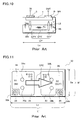
- Fig. 10 shows a schematic view of a current path when an electrode (for example, a source electrode S) connected to an input terminal IN and an electrode (for example, a drain electrode D) connected to an output terminal OUT are provided on a first main surface Sf1 of a discrete semiconductor MOSFET as in the case of Japanese Patent Application Publication No. 2002-368218 .
- an electrode for example, a source electrode S
- an electrode for example, a drain electrode D
- a substrate is formed by stacking a low-concentration semiconductor layer LS on a high-concentration semiconductor substrate HS, and an element region e of the MOSFET is provided in the surface of the low-concentration semiconductor layer LS.
- a current path CP' is mainly formed from the source electrode S on the first main surface Sf1 to the low-concentration semiconductor layer LS then to the high-concentration semiconductor substrate HS, back to the low-concentration semiconductor layer LS, and then to the drain electrode D.
- the current path CP' includes first current paths CP1', which are components mainly in vertical directions of the substrate, and a second current path CP2', which is a component mainly in a horizontal direction of the substrate. Accordingly, the resistance of the current path CP' from the source electrode S to the drain electrode D of the MOSFET is obtained by combining resistances Ra and Rc in the vertical directions of the substrate and a resistance Rb in the horizontal direction of the substrate.
- the current path in the horizontal direction is formed in or near the metal layer, which has a low resistance.
- the resistance Rb in the horizontal direction can be reduced.
- the second current path CP2' is formed mainly in the high-concentration semiconductor substrate (for example, a silicon substrate) HS. Since the resistance of the high-concentration semiconductor substrate HS is higher than that of the metal layer, the resistance Rb in the horizontal direction depends more on the shape of the second current path CP2'.
- the shape of the current path in the horizontal direction is determined by the shape of the chip (semiconductor substrate). Particularly, when the planar shape of the chip is approximately rectangular as shown in Fig. 9, the resistance Rb is significantly influenced by this shape.
- Fig. 11 schematically shows a second current path of the MOSFET shown in Fig. 9.
- Fig. 11 for example, two of the first source bump electrodes 35b, which are connected to the input terminal, are disposed on the first MOSFET 31.
- two of the second source bump electrodes 36b which are connected to the output terminal, are disposed on the second MOSFET 32.
- the second current paths CP2' are formed between the first source bump electrodes 35b and the second source bump electrodes 36b as shown by the arrow.
- the planar shape of the chip is rectangular, and the electrodes connected to the input and output terminals are disposed on the first main surface Sf1 of the chip.
- This invention provides a semiconductor device including a rectangular semiconductor substrate, a discrete semiconductor element disposed on a first portion of a first primary plane of the rectangular semiconductor substrate, a first electrode disposed on the first portion of the first primary plane, and a second electrode disposed on a second portion of the first primary plane, wherein the device is configured to form a current path comprising a first path from the first electrode to a first part of the substrate below the first electrode, a second path from the first part to a second part of the substrate below the second electrode, and a third path from the second part of the substrate to the second electrode, and the second path is parallel to a short side of the rectangular semiconductor substrate.
- This invention also provides a semiconductor device including a rectangular semiconductor substrate comprising two long sides and two short sides, an elongated input electrode disposed on a first surface of the substrate along one of the long sides of the substrate so that a direction of the elongation of the input electrode is parallel to the long sides, and an output electrode disposed on the first surface of the substrate between the elongated input electrode and another of the long sides of the substrate, wherein the rectangular semiconductor substrate comprises a high impurity substrate and a low impurity layer formed on the high impurity substrate, and the input electrode and the output electrode are electrically connected through the high impurity substrate.
- This invention also provides a semiconductor device including a rectangular semiconductor substrate comprising two long sides and two short sides, a first elongated discrete semiconductor element disposed on a first surface of the substrate along one of the long sides of the substrate so that a direction of the elongation of the first elongated discrete semiconductor element is parallel to the long sides, and a second elongated discrete semiconductor element disposed on the first surface of the substrate along another of the long sides of the substrate so that a direction of the elongation of the second elongated discrete semiconductor element is parallel to the long sides, wherein the rectangular semiconductor substrate comprises a high impurity substrate and a low impurity layer formed on the high impurity substrate, and the first and second discrete semiconductor elements are electrically connected through the high impurity substrate.
- a resistance of a substrate in a horizontal direction can be reduced.
- first bump electrodes connected to input terminals and second bump electrodes connected to output terminals are provided, and the first and second bump electrodes which are positioned closest to each other among the first and second bump electrodes are arranged so that the straight line between the first and second bump electrodes can be parallel to the short side of the chip, each resistance between the electrodes provided on the first main surface can be reduced accordingly.
- the present invention can significantly contribute to the reduction in the resistance in a semiconductor device, the resistance of which largely depends on the shape of a current path in a horizontal direction of a substrate.
- the reduction is significant especially in the case of a bare chip which is mounted by a flip chip mounting, and which achieves lower cost by omitting a metal layer to be formed on a second main surface.
- a semiconductor device includes a semiconductor substrate, an element region, a first electrode and a second electrode.
- the first and second electrodes are provided on a first main surface of the semiconductor substrate.
- a current path is formed from the first electrode to the second electrode through the inside of the semiconductor substrate.
- a discrete semiconductor element In the element region, a discrete semiconductor element is formed.
- a discrete semiconductor element is also called an individual semiconductor and is a collective term for single-function semiconductor elements.
- Examples of the discrete semiconductor elements are a field-effect transistor (FET) typified by a MOSFET (Metal Oxide Semiconductor Field Effect Transistor), an IGBT (Insulated Gate Bipolar Transistor) and a junction FET, a bipolar transistor, a diode, a thyristor and the like.
- FET field-effect transistor
- Fig. 1A to Fig. 5C show, as an example of a first embodiment, a case where an n channel MOSFET is formed in the element region, and where a source electrode and drain electrodes are provided on a first main surface Sf1.
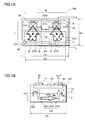
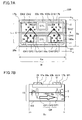
- Fig. 1A and Fig. 1B are schematic diagrams showing a MOSFET 100 according to this embodiment.
- Fig. 1A is a plan view of the MOSFET 100
- Fig. 1B is a schematic cross-sectional view taken along the line a-a in Fig. 1A.
- a semiconductor substrate (semiconductor chip) 10 has the first main surface Sf1 and a second main surface (unillustrated here) on the reverse side of the first main surface Sf1.
- the shape of the semiconductor substrate 10 is, for example, approximately rectangular, having a long side Le and a short side Se.
- the length of the long side Le is 1.5 mm
- that of the short side Se is 1.0 mm.
- an element region 20 of the MOSFET is provided on the first main surface Sf1 of the semiconductor substrate 10.
- a source electrode 17 is provided on the element region 20, the source electrode 17 being connected to the element region 20 via an insulating film or the like having a desired opening.
- drain electrodes 18 and a gate pad electrode 19 are provided on the first main surface Sf1, and are also electrically connected to the element region 20 via an insulating film or the like having a desired opening.
- the source electrode 17, the drain electrodes 18 and the gate pad electrode 19 are connected to a lead frame or a circuit board to serve as an external terminal via connecting, such as a bump electrode, a bonding wire and a metal plate.
- the source electrode 17 is connected to an input terminal IN
- the drain electrodes 18 are connected to output terminals OUT
- the gate pad electrode 19 is connected to a control terminal CTL. Accordingly, a current path is formed from the source electrode 17 to each of the drain electrodes 18 in the semiconductor substrate 10. Note that, in this embodiment, the source electrode 17 and the drain electrodes 18 respectively connected to the input terminal and the output terminals can be replaced with each other while the same result is obtained.
- the semiconductor substrate 10 is formed by stacking a low-concentration semiconductor layer 2 on a high-concentration semiconductor substrate 1, and the element region 20 of the MOSFET is provided in the surface of the low-concentration semiconductor layer 2. The detail will be described later.
- the source electrode 17 connected to the input terminal IN and the drain electrodes 18 connected to the output terminals OUT are disposed on the first main surface Sf1 as described above.
- the current paths CP are formed from the source electrode 17 to each of the drain electrodes 18 in the semiconductor substrate 10.
- the current path CP includes first current paths CP1, which are components approximately vertical to the first main surface Sf1, and a second current path CP2, which is a component approximately horizontal to the first main surface Sf1.
- the first current paths CP1 include a path from the source electrode 17 to the high-concentration semiconductor substrate 1 through the low-concentration semiconductor layer 2, and a path from the high-concentration semiconductor substrate 1 to the drain electrode 18 through the low-concentration semiconductor layer 2.
- the second current path CP2 is a path formed in a horizontal direction of the semiconductor substrate 10 from mainly the high-concentration semiconductor substrate 1 and the low-concentration semiconductor layer 2 near the substrate 1 below the source electrode 17 to mainly the high-concentration semiconductor substrate 1 and the low-concentration semiconductor layer 2 near the substrate 1 below the drain electrodes 18.
- a layout for the element region 20 of the semiconductor substrate 10 is designed as follows.
- the main direction of the second current path CP2 is formed along the short side Se of the semiconductor substrate (chip) 10, that is, the direction in which current flows in the second current path CP2 is the direction in which the short side Se extends.
- the width of the path CP2 in which the current flows is parallel to the direction in which the long side Le extends.
- the semiconductor substrate 10 is partitioned into a first region r1 and a second region r2 by the line along the long side Le (see the chain double-dashed line) for convenience of the description.
- the element region 20 and the source electrode 17 are provided in the input side of the second current paths CP2 in the direction of the formation (the direction in which current flows).
- the drain electrodes 18 and a conductive path (for example, a high-concentration impurity region) 22 are provided.
- the drain electrodes 18 respectively are provided in the output side of the respective second current paths CP2 in the direction of forming the current paths CP2.
- the conductive path 22 connects the element region 20 to the drain electrodes 18.
- the first region r1 (element region 20) and the second region r2 (conductive path 22) are arranged in the manner of being aligned along the short side Se of the semiconductor substrate 10, and thereby the second current path CP2 is formed in a direction along the short side Se of the semiconductor substrate 10.
- the shape of the semiconductor substrate 10 is rectangular, when the second current path CP2 is formed in the direction along the short side Se of the semiconductor substrate 10, a width W of the second current path CP2 is enlarged, and a length L thereof is shortened.
- the area for the width W is sufficiently secured in parallel to the direction of the long side Le, and the length L is made equal to or shorter than the short side Se.
- the resistance of the second current path CP2 in this embodiment can be reduced compared with the case of, for example, forming the second current path CP2' having the length L' in the direction of the long side Le of the semiconductor substrate 10 and the width W' parallel to the direction of the short side Se thereof as shown in Fig. 11.
- this embodiment includes a large number of first contact holes (for example, on source regions) CH1', which electrically connect the source electrode 17 to the element region 20, and second contact holes CH2' (for example, on the regions in the conductive path 22 which are in contact with the drain electrodes 18), which electrically connect the drain electrodes 18 to the element region 20.
- first contact holes CH1' are formed in the insulating film (unillustrated) on the first region r1 of the substrate 10.
- the second contact holes CH2' are formed in the insulating film (unillustrated) on the second region r2 of the substrate 10.
- the second contact hole CH2' is larger than the first contact hole CH1'.
- a set of a first contact hole CH1 and a second contact hole CH2 which come closest to each other is aligned in the direction along the short side Se.
- the main direction of the second current path CP2 is formed along the short side Se.
- the pattern and the arrangement of these electrodes 17 and 18 are not limited to the above case.
- Fig. 1A shows a case in which the element region 20 is in a rectangular shape a long side Le' of which is approximately equal to the long side Le of the semiconductor substrate 10. Nevertheless, as long as the second current paths CP2 are formed in the direction along the short side Se of the semiconductor substrate 10, the pattern of the element region 20 is not limited to the one illustrated in Fig. 1A.
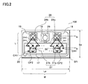
- Fig. 2 is a plan view showing that bump electrodes to be respectively connected to the source electrode 17, the drain electrodes 18 and the gate pad electrode 19 are provided in this embodiment.
- the source electrode 17, the drain electrodes 18 and the gate pad electrode 19 are respectively provided with source bump electrodes 27, drain bump electrodes 28 and a gate bump electrode 29 thereon. These bump electrodes serve as external connection electrodes, and are shown by circles.
- the source bump electrodes 27 and the drain bump electrodes 28 are respectively connected to the input terminals IN and the output terminals OUT of the MOSFET.
- the gate bump electrode 29 is connected to the control terminal CTL.
- Fig. 2 shows that the two source bump electrodes 27 and the two drain bump electrodes 18 are provided, and specifically a total of five bump electrodes are provided, that is, source bump electrodes 27a and 27b, drain bump electrodes 28a and 28b, and the gate bump electrode 29. Note that, the number of each bump electrode 27, 28 and 29 is not limited to the one illustrated.
- the straight line between a first bump electrode (source bump electrode 27) and a second bump electrode (drain bump electrode 28) is arranged along the short side Se so as to be parallel to the short side Se, the first bump electrode and the second bump electrode being positioned closest to each other among the bump electrodes respectively connected to the input and output terminals.
- the set (of the source bump electrode 27a and the drain bump electrode 28a) which has the closest distance among the combinations of the first and second bump electrodes is provided in the direction along the short side Se.
- the main direction of the second current paths CP2 is formed along the short side Se.
- Each electrode (source electrode 17, drain electrode 18, source bump electrode 27 and drain bump electrode 28) on the first main surface Sf1 also has a great influence on the resistance of the semiconductor device. For example, when each electrode and a wire connected thereto are arranged around on the first main surface Sf1, the amount of the resistance component in the horizontal direction is also increased.
- the first bump electrode (source bump electrode 27) and the second bump electrode (drain bump electrode 28) which are positioned closest to each other are aligned in the direction along the short side Se.
- the second current path CP2 formed along the short side Se is connected to external terminals (the input terminal IN and the output terminal OUT) without being arranged around in the horizontal direction on the first main surface Sf1.
- the resistance of each electrode in the horizontal direction is also reduced as much as possible, resulting in significantly contributing to the reduction in the resistance of the device.
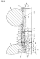
- Fig. 3 is a cross-sectional view showing the MOSFET 100 in detail, and corresponds to the cross section taken along the line b-b in Fig. 2.
- the semiconductor substrate 10 has the first main surface Sf1 and a second main surface Sf2, and is provided with the element region 20 of the MOSFET 100.
- the semiconductor substrate 10 is formed by stacking the n- type semiconductor layer (for example, an n- type epitaxial layer) 2 on the n+ type silicon semiconductor substrate 1, and thereby a drain region is formed.
- Trenches 7 are formed so as to reach the n- type semiconductor layer 2, penetrating through the channel layer 4. Generally, the trenches 7 are patterned into a lattice or stripe shape in the plane pattern of the first main surface Sf1.
- a gate oxide film 11 is provided on the inner wall of each of the trenches 7.
- the thickness of the gate oxide film 11 is approximately several hundred ⁇ in accordance with a driving voltage of the MOSFET.
- a conductive material is buried inside the trench 7 to form a gate electrode 13.
- the conductive material is, for example, a polysilicon to which, for example, n type impurities are introduced in order to reduce the resistance.
- Source regions 15 are n+ type impurity regions formed by implanting n type impurities in regions of the surface of the channel layer 4, the regions adjacent to the trenches 7. Moreover, a body region 14, which is a diffusion region of p+ type impurities, is formed in a region of the surface of the channel layer 4, the region between the source regions 15 adjacent to each other. Thereby, the electric potential of the substrate is stabilized. Accordingly, the portion surrounded by the trenches 7 adjacent to each other forms one cell of a MOS transistor. A large number of these cells collectively constitute the element region 20 of the MOSFET.
- the element region 20 extends across the region where the cells of the MOS transistor positioned on the outermost periphery are provided.
- the gate electrode 13 is covered by an interlayer insulating film 16.
- the source electrode 17 is a metal electrode formed by sputtering aluminium (Al) or the like and then patterning the resultant into a desired shape.
- the source electrode 17 covers the element region 20, and is provided on the first main surface Sf1 of the semiconductor substrate 10.
- the source electrode 17 is connected to the source regions 15 and the body regions 14 through multiple contact holes (the first contact holes CH1') formed in the interlayer insulating film 16.
- the gate electrode 13 is pulled onto the substrate 10 by connecting portion 13c, and is extended to a gate connecting electrode 19, which surrounds the periphery of the semiconductor substrate 10, and thereby connected to the gate pad electrode (unillustrated here).
- a nitride film 23 is provided on the source electrode 17, and an opening is made in a predetermined region of the nitride film 23 to form a under bump metal (UBM) 24.
- the UBM 24 is a metal layer formed by stacking nickel (Ni: 2.4 ⁇ m in thickness) and gold (Au: 500 ⁇ in thickness) in this order from the lower layer by electrodes plating, for example.
- a solder resist 25 from which the UBM 24 is exposed, is provided.
- the source bump electrode 27 is formed by a screen printing using the UBM 24 as a bottom electrode. The diameter of the source bump electrode 27 is approximately 250 ⁇ m.
- Fig. 3 shows a case that the source bump electrode 27 is disposed on an edge portion of the element region 20 for convenience of the description. However, in reality, the source bump electrode 27 is arranged so that the source potential can be applied to the element region 20 uniformly.
- the drain electrode 18 is provided on the first main surface Sf1 of the semiconductor substrate 10.
- the drain electrode 18 is formed by patterning a metal layer (for example, Al), which is the same as that used in the source electrode 17, into a desired shape, and is placed with a space between the drain electrode 18 and the source electrode 17.
- the drain bump electrode 28 is provided above the drain electrode 18 as in the case of the source bump electrode 27.
- the conductive path 22 which extracts the current from the element region 20, is provided below the drain electrode 18, the conductive path 22, which extracts the current from the element region 20, is provided.
- the conductive path 22 is formed of, for example, an n type high-concentration impurity region (n+ type impurity region) 22a and an n+ type impurity region 22b to be the second contact hole CH2.
- the conductive path 22 reaches the n+ type silicon semiconductor substrate 1 from the surface of the n- type semiconductor layer 2.
- the drain electrode 18 is connected to the drain region (the n- type semiconductor layer 2 and the n+ type silicon semiconductor substrate 1) of the element region 20 via the conductive path 22.
- a metal layer is provided on the bottom surface (second main surface Sf2) to reduce the resistance.
- the metal layer on the bottom surface is not intended to be used as an electrode.
- the metal layer is omitted in some cases, particularly in a product which is critical in terms of cost.
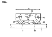
- Fig. 4 shows a side view of a circuit board (printed board) or the like on which the flip chip mounting is performed as an example of a semiconductor substrate (semiconductor chip) 10.
- Fig. 4 is a drawing viewed in the direction of a short side Se of the chip. The illustration of an element region 20 and the like of the semiconductor substrate 10 will be omitted in Fig. 4.
- the semiconductor chip 10 is disposed, while facing down, on a circuit board 51 provided with conductive patterns 52.
- a source bump electrode 27, a drain bump electrode 28 and a gate bump electrode are aligned with the corresponding conductive patterns 52, and then adhered and connected thereto by reflow soldering with heat or using the ultrasonic vibration under a pressurized condition.
- a first main surface Sf1 is provided with a source electrode (source bump electrode 27) connected to an input terminal, and a drain electrode (drain bump electrode 28) connected to output terminals. Accordingly, at the time of operating a MOSFET 100, a current path is formed mainly from the source electrode (source bump electrode 27) to the drain electrode (drain bump electrode 28) through the semiconductor substrate 10 (the element region 20, an n- type semiconductor layer 2, an n+ type silicon semiconductor substrate 1 and a conductive path 22) as shown by the arrow in Fig. 4.
- the element region 20 and the conductive path 22 are arranged so that a second current path CP2, which significantly influences the resistance of the semiconductor device, can be formed in a direction along the short side Se of the semiconductor substrate 10.
- a first contact hole CH1 and a second contact hole CH2 which are positioned closest to each other, and which are respectively connected to the input and output terminals, as well as the source bump electrode 27 and the drain bump electrode 28 which are positioned closest to each other and, which are respectively connected to the input and output terminals, are aligned along the short side Se (see Fig. 1A and Fig. 1B).
- a width W of the second current path CP2 is sufficiently secured along a long side Le of the semiconductor substrate 10, and a length L of the second current path CP2 is made equal to or shorter than the short side Se.
- a resistance Rb of the substrate 10 in a horizontal direction is greatly reduced, resulting in significantly contributing to the reduction in the resistance of the device.
- the bump electrodes to serve as external connection electrodes may not be disposed in the pattern shown in Fig. 2 in some cases due to the terminal layout for the circuit board 52 on which the semiconductor substrate (chip) 10 is mounted.
- Figs. 5A to 5C are plan views showing one example of the multilayer electrode structure, and specifically showing that each electrode of the element region 20 has a two-layer electrode structure.
- Fig. 5A shows electrodes in a first layer.
- Fig. 5B shows the electrodes in the first layer and electrodes in a second layer.
- Fig. 5C shows the second layer and bump electrodes.
- the semiconductor substrate 10 is the same as that of Fig. 1A and Fig. 1B, and partitioned into a first region r1 and a second region r2.
- the first region r1 is provided with the element region 20.
- the second region r2 is provided with the unillustrated conductive path.
- a gate pad electrode and the gate bump electrode are omitted in the drawings, but are disposed in desired positions (for example, positions along the short side Se).
- first contact holes CH1' and a second contact hole CH2 are provided to an insulating film (unillustrated), which covers the substrate 10.
- a first source electrode 171 for the first layer is disposed on the first contact holes CH1', and a first drain electrode 181 for the first layer is disposed on the second contact hole CH2.
- the electrode structures in the first and second layers are arranged so that the electrodes in one layer cross those in the other layer.
- an insulating film (unillustrated) is further disposed on the first source electrode 171 and the first drain electrode 181, and openings are made in desired positions of the insulating film to form through holes TH.
- One of the through holes TH is formed in the insulating film by the side of the first source electrode 171, and the other hole TH is formed in the insulating film by the side of the first drain electrode 181.
- a second source electrode 172 and a second drain electrode 182 in the second layer are arranged so as to cross the first source electrode 171 and the first drain electrode 181, respectively.
- source bump electrodes 27a and 27b are provided on the second source electrode 172.
- Drain bump electrodes 28a and 28b are provided on the second drain electrode 182.
- the resistance of a wire is somewhat increased by arranging the wiring around within the structure.
- the layouts of the first region r1 (element region 20) and the second region r2 is designed so that the second current path CP2 can be formed along the short side Se of the semiconductor substrate 10 (see Fig. 5A).
- the resistance Rb of the substrate 10 in the horizontal direction is reduced, resulting in significantly contributing to the reduction in the resistance of the device.
- an element region 20 provided to a semiconductor substrate (semiconductor chip) 10 the number thereof may be plural as long as the element regions are discrete (single-function) semiconductors.
- description will be given, as an example, in a case where two element regions 20a and 20b of a first MOSFET 100a and a second MOSFET 100b, respectively, are integrated into the single semiconductor substrate (semiconductor chip) 10 while sharing a drain.
- MOSFET semiconductor device
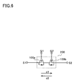
- Fig. 6 is a circuit diagram showing an example where a semiconductor device (switching element) capable of switching current paths in both directions is constituted of a MOSFET.
- the first MOSFET 100a and the second MOSFET 100b each constituted of a large number of MOS transistor cells are connected to each other in serial while sharing a drain D of the MOSFETs.
- a gate signal is applied to gate terminals G1 and G2 to control both MOSFETs, and the current paths are switched in response to the potential difference between a first source terminal S1 and a second source terminal S2.
- Each of the first MOSFET 100a and the second MOSFET 100b includes a parasitic diode.
- the first MOSFET 100a is turned off, and the second MOSFET 100b is turned on by a control signal.
- a current path in a d1 direction is formed by the parasitic diode of the first MOSFET 100a and the second MOSFET 100b.
- the first MOSFET 100a is turned on, and the second MOSFET 100b is turned off by a control signal.
- a current path in a d2 direction is formed by the first MOSFET 100a and the parasitic diode of the second MOSFET 100b.
- Fig. 7A and Fig. 7B show an example of the above-mentioned switching element 200.
- Fig. 7A is a plan view showing the electrodes respectively connected to input, output and control terminals of the switching element 200.
- Fig. 7B is a schematic cross-sectional view taken along the line c-c in Fig. 7A.
- the first element region 20a and the second element region 20b identical to each other are provided to the semiconductor substrate (chip) 10 in an approximately rectangular shape having a long side Le and a short side Se.
- the first element region 20a is for the first MOSFET 100a
- the second element region 20b is for the second MOSFET 100b.
- the element region 20a and the element region 20b respectively of the first MOSFET 100a and the second MOSFET 100b are arranged in line symmetry about the center line X-X extending in a direction along the long side Le of the semiconductor substrate 10.
- a first source electrode 17a and a first gate pad electrode 19a are provided to the first element region 20a side.
- a second source electrode 17b and a second gate pad electrode 19b are provided to the second element region 20b side.
- a source region (unillustrated) of the first MOSFET 100a is connected to the first source electrode 17a, which covers the first element region 20a.
- a gate electrode (unillustrated) of the first MOSFET 100a is extended to the periphery of the semiconductor substrate 10, and is connected to the first gate pad electrode 19a.
- the second MOSFET 100b has the same configuration.
- the first MOSFET 100a and the second MOSFET 100b are provided to the same semiconductor substrate 10 having a first main surface Sf1 and a second main surface Sf2.
- the first MOSFET 100a is provided to the first element region 20a of the semiconductor substrate 10
- the second MOSFET 100b is provided to the second element region 20b.
- the first MOSFET 100a and the second MOSFET 100b share the drain region.
- each element region 20a and 20b is the same as that of the first embodiment, and thus the description thereof will be omitted. In the second embodiment, however, a drain terminal is not exposed to the outside, and a drain electrode is not provided.
- first source electrode 17a the first gate pad electrode 19a, the second source electrode 17b and the second gate pad electrode 19b are provided on the first main surface Sf1.
- the specific structure of these electrode portions is the same as that in the first embodiment.
- the configurations of the first MOSFET 100a and the second MOSFET 100b are the same.
- both the first source electrode 17a and the second source electrode 17b are provided on the first main surface Sf1 of the semiconductor substrate 10, and serve as a first electrode and a second electrode respectively connected to the input and output terminals. Then, a current path is formed between the electrodes.
- a control signal is applied to the first gate pad electrode 19a and the second gate pad electrode 19b.
- the first MOSFET 100a is turned off, and the second MOSFET 100b is tuned on.
- the potential of the first source electrode 17a is made higher than that of the second source electrode 17b, the current path is formed in the d1 direction in Fig. 6.
- the potential of the first source electrode 17a is made lower than that of the second source electrode 17b, and thereby the current path is formed in the d2 direction opposite to the d1 direction.
- the current path in the d1 or d2 direction is formed without using the parasitic diodes, but in response to the potential difference between the first source electrode 17a and the second source electrode 17b.
- the current path is formed from the first source electrode 17a of the first MOSFET 100a to the second source electrode 17b of the second MOSFET 100b (or in the opposite direction) through the semiconductor substrate 10.
- the layout for the element regions 20a, 20b and the like of the semiconductor substrate 10 is designed so that the main direction of second current paths CP2 can be formed along the short side Se of the semiconductor substrate (chip) 10.
- the description will be given with the simplest example as follows.
- the semiconductor substrate 10 is partitioned into a first region r1 and a second region r2 by the center line X-X extending along the long side Le for convenience of the description.
- the first element region 20a and the first source electrode 17a are provided in the input side of the second current path CP2.
- the second element region 20b and the second source electrode 17b are provided in the output side of the second current path CP2.
- the second current path CP2 is formed in a direction along the short side Se of the semiconductor substrate 10. Thereby, a resistance Rb of the second current path CP2 in the horizontal direction is greatly reduced.
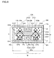
- Fig. 8 shows a case in which bump electrodes are disposed on the semiconductor device in Fig. 7A and Fig. 7B as shown by circles.
- First source bump electrodes 27a (27a1 and 27a2) are formed on, and connected to the first source electrodes 17a, respectively.
- Second source bump electrodes 27b (27b1 and 27b2) are formed on, and connected to, the second source electrodes 17b, respectively.
- a first gate bump electrode 29a and a second gate bump electrode 29b are formed on the first gate pad electrode 19a and the second gate pad electrode 19b, respectively.
- first contact holes CH1' which connect the first source electrode 17a to the first element region 20a
- second contact potions CH2' which connect the second source electrode 17b to the second element region 20b.
- a set of a first contact hole CH1 and a second contact hole CH2 which are positioned closest to each other is aligned along the short side Se so as to be parallel to the short side Se.
- each bump electrode 27a, 27b, 29a and 29b is not limited to the one illustrated.
- first bump electrode first source bump electrode 27a1
- second bump electrode second source bump electrode 27b1
- the second current path CP2 formed along the short side Se is connected to external terminals (the input terminal and the output terminal) without being arranged around in the horizontal direction on the first main surface Sf1. Accordingly, the resistance of each electrode in the horizontal direction is also reduced as much as possible, resulting in significantly contributing to the reduction in the resistance of the device.
- the present invention is not limited to this.
- the present invention can be implemented to a p channel MOSFET, which has the opposite conductive type as above.
- the present invention is not limited to these, and can be implemented to a bipolar transistor or a diode as above, and the same effect is obtainable.
- An element region is provided with a base region of one conductivity type in a semiconductor substrate of an opposite conductivity type serving as a collector region, and an emitter region of the opposite conductivity type is provided to the surface of the base region.
- This element region 20 is provided to a first region r1 as shown in Fig. 1A and Fig. 1B.
- a conductive path 22 connected to the collector region is provided to a second region r2.
- an emitter electrode connected to the emitter region and collector electrodes connected to the collector region are provided in the patterns of the source electrode 17 and the drain electrodes 18, respectively, as shown in Fig. 1A and Fig. 1B.
- a base electrode connected to the base region is provided in the pattern of the gate pad electrode 19 in Fig. 1A.
- the bump electrodes are provided as shown in Fig. 2.
- emitter bump electrodes, collector bump electrodes and a base bump electrode are provided in the positions of the source bump electrodes 27, the drain bump electrodes 28 and the gate bump electrode 29, respectively.
- a second current path CP2 is formed in a direction along a short side Se of a substrate 10 as shown in Fig. 1A and Fig. 1B.
- An element region 20 is provided with an impurity region of one conductivity type, which is connected to an anode electrode in a semiconductor substrate of an opposite conductivity type, which is connected to cathode electrodes.
- the element region 20 is provided to a first region r1 as shown in Fig. 1A.
- a conductive path 22 connected to the semiconductor substrate of the opposite conductivity type is provided to a second region r2.
- the anode electrode and the cathode electrodes are provided in the patterns of the source electrode 17 and the drain electrodes 18, respectively, as shown in Fig. 1A and Fig. 1B.
- the bump electrodes are provided as shown in Fig. 2.
- anode bump electrodes and cathode bump electrodes are provided in the positions of the source bump electrodes 27 and the drain bump electrodes 28, respectively.
- a second current path CP2 is formed in a direction along a short side Se of a substrate 10 as shown in Fig. 1A and Fig. 1B.
Landscapes
- Semiconductor Integrated Circuits (AREA)
- Insulated Gate Type Field-Effect Transistor (AREA)
- Metal-Oxide And Bipolar Metal-Oxide Semiconductor Integrated Circuits (AREA)
- Wire Bonding (AREA)
- Electrodes Of Semiconductors (AREA)
Abstract
Description
- This application claims priority from Japanese Patent Application Number
JP 2006-292234 filed October 27, 2006 - The present invention relates to a semiconductor device, particularly to a semiconductor device which can reduce a resistance in a flip chip mounting.
- In many discrete semiconductor devices (semiconductor chips), electrodes, respectively connected to an input terminal and an output terminal, are each provided to a different surface of the main surfaces (top surface and bottom surface) of the chip. On the other hand, also known has been a structure that makes a flip chip mounting possible by providing, on one main surface of the chip, a source electrode and a drain electrode respectively connected to an input terminal and an output terminal as well as a gate electrode connected to a control terminal in a MOSFET, for example. This technology is described, for instance, in
Japanese Patent Application Publication No. 2002-368218 - Moreover, in another known structure, two MOSFETs are integrated into one chip while sharing a drain terminal, and source electrodes and gate electrodes are provided on one main surface of the chip. In this case, the mounting method is not limited to the flip chip mounting. Nevertheless, since the source electrodes of the two MOSFETs are respectively connected to the input terminal and the output terminal, the electrodes connected to an input terminal and an output terminal are provided on the one main surface of the chip as in the case of
Japanese Patent Application Publication No. 2002-368218 Japanese Patent Application Publication No. 2002-118258 - With reference to Fig. 9, description will be given of a semiconductor device in which two MOSFETs are integrated into one chip as an example of the semiconductor device provided, on one main surface thereof, with an input terminal and an output terminal.
- Fig. 9 is a plan view of a
semiconductor device 30 which is formed by integrating afirst MOSFET 31 and asecond MOSFET 32 into one chip. To each of theMOSFETs first source electrode 35 and a firstgate pad electrode 33 are for theMOSFET 31 while asecond source electrode 36 and a secondgate pad electrode 34 are for theMOSFET 32. - The two MOSFETs share a substrate (drain region). The
first MOSFET 31 and thesecond MOSFET 32 are arranged, for example, in line symmetry about the center line X-X of the chip. The firstgate pad electrode 33 and the secondgate pad electrode 34 are independently disposed to the corners of the chip. - The
first source electrode 35 and a firstsource bump electrode 35b, which are connected to a first source terminal S1, are provided on a first main surface Sf1 of the chip. Thesecond source electrode 36 and a secondsource bump electrode 36b, which are connected to a second source terminal S2, are also provided on the first main surface Sf1. Similarly, the firstgate pad electrode 33 and a firstgate bump electrode 33b, which are connected to a first gate terminal G1, are provided on the first main surface Sf1. The secondgate pad electrode 34 and a secondgate bump electrode 34b, which are connected to a second gate terminal G2, are also provided on the first main surface Sf1. - In this case, a drain electrode is shared by the two
MOSFETs MOSFETs first source electrode 35 and thesecond source electrode 36. Specifically, the firstsource bump electrode 35b is an electrode connected to the input terminal (or the output terminal) of theMOSFET 30 while the secondsource bump electrode 36b is an electrode connected to the output terminal (or the input terminal) of theMOSFET 30. - Fig. 10 shows a schematic view of a current path when an electrode (for example, a source electrode S) connected to an input terminal IN and an electrode (for example, a drain electrode D) connected to an output terminal OUT are provided on a first main surface Sf1 of a discrete semiconductor MOSFET as in the case of
Japanese Patent Application Publication No. 2002-368218 - A substrate is formed by stacking a low-concentration semiconductor layer LS on a high-concentration semiconductor substrate HS, and an element region e of the MOSFET is provided in the surface of the low-concentration semiconductor layer LS.
- In the structure where the source electrode S and the drain electrode D are provided on the first main surface Sf1 of the chip, a current path CP' is mainly formed from the source electrode S on the first main surface Sf1 to the low-concentration semiconductor layer LS then to the high-concentration semiconductor substrate HS, back to the low-concentration semiconductor layer LS, and then to the drain electrode D. In other words, the current path CP' includes first current paths CP1', which are components mainly in vertical directions of the substrate, and a second current path CP2', which is a component mainly in a horizontal direction of the substrate. Accordingly, the resistance of the current path CP' from the source electrode S to the drain electrode D of the MOSFET is obtained by combining resistances Ra and Rc in the vertical directions of the substrate and a resistance Rb in the horizontal direction of the substrate.
- For example, when a metal layer is formed on a second main surface Sf2 in the structure shown in Fig. 10, the current path in the horizontal direction is formed in or near the metal layer, which has a low resistance. Thereby, the resistance Rb in the horizontal direction can be reduced. However, in a bear chip or the like with which the flip chip mounting is performed, when a metal layer is not formed on the second main surface Sf2, the second current path CP2' is formed mainly in the high-concentration semiconductor substrate (for example, a silicon substrate) HS. Since the resistance of the high-concentration semiconductor substrate HS is higher than that of the metal layer, the resistance Rb in the horizontal direction depends more on the shape of the second current path CP2'.
- The shape of the current path in the horizontal direction is determined by the shape of the chip (semiconductor substrate). Particularly, when the planar shape of the chip is approximately rectangular as shown in Fig. 9, the resistance Rb is significantly influenced by this shape.
- Fig. 11 schematically shows a second current path of the MOSFET shown in Fig. 9.
- In Fig. 11, for example, two of the first
source bump electrodes 35b, which are connected to the input terminal, are disposed on thefirst MOSFET 31. For example, two of the secondsource bump electrodes 36b, which are connected to the output terminal, are disposed on thesecond MOSFET 32. Thus, the second current paths CP2' are formed between the firstsource bump electrodes 35b and the secondsource bump electrodes 36b as shown by the arrow. - In the above-described semiconductor device, the planar shape of the chip is rectangular, and the electrodes connected to the input and output terminals are disposed on the first main surface Sf1 of the chip. In the semiconductor device, the longer the length L' of the second current path CP2', which is the length between one end and the other end in the direction of a current flow, is, and the narrower the width W' of the second current path CP2' is, the larger the resistance Rb in the horizontal direction becomes. This causes a problem that the resistance of the whole device is increased.
- It is an object of this invention to provide an improved semiconductor device that lessens this drawback.
- The solution according to the invention resides in the features of the independent claims and preferably in those of the dependent claims.
- This invention provides a semiconductor device including a rectangular semiconductor substrate, a discrete semiconductor element disposed on a first portion of a first primary plane of the rectangular semiconductor substrate, a first electrode disposed on the first portion of the first primary plane, and a second electrode disposed on a second portion of the first primary plane, wherein the device is configured to form a current path comprising a first path from the first electrode to a first part of the substrate below the first electrode, a second path from the first part to a second part of the substrate below the second electrode, and a third path from the second part of the substrate to the second electrode, and the second path is parallel to a short side of the rectangular semiconductor substrate.
- This invention also provides a semiconductor device including a rectangular semiconductor substrate comprising two long sides and two short sides, an elongated input electrode disposed on a first surface of the substrate along one of the long sides of the substrate so that a direction of the elongation of the input electrode is parallel to the long sides, and an output electrode disposed on the first surface of the substrate between the elongated input electrode and another of the long sides of the substrate, wherein the rectangular semiconductor substrate comprises a high impurity substrate and a low impurity layer formed on the high impurity substrate, and the input electrode and the output electrode are electrically connected through the high impurity substrate.
- This invention also provides a semiconductor device including a rectangular semiconductor substrate comprising two long sides and two short sides, a first elongated discrete semiconductor element disposed on a first surface of the substrate along one of the long sides of the substrate so that a direction of the elongation of the first elongated discrete semiconductor element is parallel to the long sides, and a second elongated discrete semiconductor element disposed on the first surface of the substrate along another of the long sides of the substrate so that a direction of the elongation of the second elongated discrete semiconductor element is parallel to the long sides, wherein the rectangular semiconductor substrate comprises a high impurity substrate and a low impurity layer formed on the high impurity substrate, and the first and second discrete semiconductor elements are electrically connected through the high impurity substrate.
- According to the present invention, firstly, a resistance of a substrate in a horizontal direction can be reduced.
- This can be achieved because, in a semiconductor device provided with electrodes connected to input and output terminals on a first main surface of the rectangular-shaped chip, an element region is arranged so that the current path in a horizontal direction of a substrate can be formed along a direction of a short side of the chip.
- Secondly, since first bump electrodes connected to input terminals and second bump electrodes connected to output terminals are provided, and the first and second bump electrodes which are positioned closest to each other among the first and second bump electrodes are arranged so that the straight line between the first and second bump electrodes can be parallel to the short side of the chip, each resistance between the electrodes provided on the first main surface can be reduced accordingly.
- Thirdly, the present invention can significantly contribute to the reduction in the resistance in a semiconductor device, the resistance of which largely depends on the shape of a current path in a horizontal direction of a substrate. The reduction is significant especially in the case of a bare chip which is mounted by a flip chip mounting, and which achieves lower cost by omitting a metal layer to be formed on a second main surface.
-
- Fig. 1A is a plan view, and Fig. 1B is a side view, for describing a semiconductor device according to a first embodiment of the present invention.
- Fig. 2 is a plan view for describing the semiconductor device according to the first embodiment of the present invention.
- Fig. 3 is a cross-sectional view for describing the semiconductor device according to the first embodiment of the present invention.
- Fig. 4 is a side view for describing the semiconductor device according to the first embodiment of the present invention.
- Fig. 5A to Fig. 5C are plan views for describing the semiconductor device according to the first embodiment of the present invention.
- Fig. 6 is a circuit diagram for describing a semiconductor device according to a second embodiment of the present invention.
- Fig. 7A is a plan view, and Fig. 7B is a side view, for describing the semiconductor device according to the second embodiment of the present invention.
- Fig. 8 is a plan view for describing the semiconductor device according to the second embodiment of the present invention.
- Fig. 9 is a plan view for describing a first conventional semiconductor device.
- Fig. 10 is a side view for describing a second conventional semiconductor device.
- Fig. 11 is a plan view for describing the first conventional semiconductor device.
- Description will be given, in detail, of embodiments of the present invention with reference to Fig. 1A to Fig. 8.
- A semiconductor device according to the embodiments present invention includes a semiconductor substrate, an element region, a first electrode and a second electrode. The first and second electrodes are provided on a first main surface of the semiconductor substrate. A current path is formed from the first electrode to the second electrode through the inside of the semiconductor substrate.
- In the element region, a discrete semiconductor element is formed. A discrete semiconductor element is also called an individual semiconductor and is a collective term for single-function semiconductor elements. Examples of the discrete semiconductor elements are a field-effect transistor (FET) typified by a MOSFET (Metal Oxide Semiconductor Field Effect Transistor), an IGBT (Insulated Gate Bipolar Transistor) and a junction FET, a bipolar transistor, a diode, a thyristor and the like.
- Fig. 1A to Fig. 5C show, as an example of a first embodiment, a case where an n channel MOSFET is formed in the element region, and where a source electrode and drain electrodes are provided on a first main surface Sf1.
- Fig. 1A and Fig. 1B are schematic diagrams showing a
MOSFET 100 according to this embodiment. Fig. 1A is a plan view of theMOSFET 100, and Fig. 1B is a schematic cross-sectional view taken along the line a-a in Fig. 1A. - As shown in Fig. 1A, a semiconductor substrate (semiconductor chip) 10 has the first main surface Sf1 and a second main surface (unillustrated here) on the reverse side of the first main surface Sf1. The shape of the
semiconductor substrate 10 is, for example, approximately rectangular, having a long side Le and a short side Se. As an example, the length of the long side Le is 1.5 mm, and that of the short side Se is 1.0 mm. - As shown by a dotted line, an
element region 20 of the MOSFET is provided on the first main surface Sf1 of thesemiconductor substrate 10. Asource electrode 17 is provided on theelement region 20, thesource electrode 17 being connected to theelement region 20 via an insulating film or the like having a desired opening. Moreover,drain electrodes 18 and agate pad electrode 19 are provided on the first main surface Sf1, and are also electrically connected to theelement region 20 via an insulating film or the like having a desired opening. - The
source electrode 17, thedrain electrodes 18 and thegate pad electrode 19 are connected to a lead frame or a circuit board to serve as an external terminal via connecting, such as a bump electrode, a bonding wire and a metal plate. - Specifically, for example, the
source electrode 17 is connected to an input terminal IN, thedrain electrodes 18 are connected to output terminals OUT, and thegate pad electrode 19 is connected to a control terminal CTL. Accordingly, a current path is formed from thesource electrode 17 to each of thedrain electrodes 18 in thesemiconductor substrate 10. Note that, in this embodiment, thesource electrode 17 and thedrain electrodes 18 respectively connected to the input terminal and the output terminals can be replaced with each other while the same result is obtained. - Description will be given of a current path CP with reference to Fig. 1B.
- The
semiconductor substrate 10 is formed by stacking a low-concentration semiconductor layer 2 on a high-concentration semiconductor substrate 1, and theelement region 20 of the MOSFET is provided in the surface of the low-concentration semiconductor layer 2. The detail will be described later. - In this embodiment, the
source electrode 17 connected to the input terminal IN and thedrain electrodes 18 connected to the output terminals OUT are disposed on the first main surface Sf1 as described above. Thus, the current paths CP are formed from thesource electrode 17 to each of thedrain electrodes 18 in thesemiconductor substrate 10. - More specifically, the current path CP includes first current paths CP1, which are components approximately vertical to the first main surface Sf1, and a second current path CP2, which is a component approximately horizontal to the first main surface Sf1. The first current paths CP1 include a path from the
source electrode 17 to the high-concentration semiconductor substrate 1 through the low-concentration semiconductor layer 2, and a path from the high-concentration semiconductor substrate 1 to thedrain electrode 18 through the low-concentration semiconductor layer 2. Additionally, the second current path CP2 is a path formed in a horizontal direction of thesemiconductor substrate 10 from mainly the high-concentration semiconductor substrate 1 and the low-concentration semiconductor layer 2 near thesubstrate 1 below thesource electrode 17 to mainly the high-concentration semiconductor substrate 1 and the low-concentration semiconductor layer 2 near thesubstrate 1 below thedrain electrodes 18. - In this embodiment, as shown in Fig. 1A and Fig. 1B, a layout for the
element region 20 of thesemiconductor substrate 10 is designed as follows. The main direction of the second current path CP2 is formed along the short side Se of the semiconductor substrate (chip) 10, that is, the direction in which current flows in the second current path CP2 is the direction in which the short side Se extends. The width of the path CP2 in which the current flows is parallel to the direction in which the long side Le extends. - The description will be given with the simplest example as follows. The
semiconductor substrate 10 is partitioned into a first region r1 and a second region r2 by the line along the long side Le (see the chain double-dashed line) for convenience of the description. In the first region r1, theelement region 20 and thesource electrode 17 are provided in the input side of the second current paths CP2 in the direction of the formation (the direction in which current flows). In the second region r2, thedrain electrodes 18 and a conductive path (for example, a high-concentration impurity region) 22 are provided. Thedrain electrodes 18 respectively are provided in the output side of the respective second current paths CP2 in the direction of forming the current paths CP2. Theconductive path 22 connects theelement region 20 to thedrain electrodes 18. The first region r1 (element region 20) and the second region r2 (conductive path 22) are arranged in the manner of being aligned along the short side Se of thesemiconductor substrate 10, and thereby the second current path CP2 is formed in a direction along the short side Se of thesemiconductor substrate 10. - Because the shape of the
semiconductor substrate 10 is rectangular, when the second current path CP2 is formed in the direction along the short side Se of thesemiconductor substrate 10, a width W of the second current path CP2 is enlarged, and a length L thereof is shortened. For example, in the layout of Fig. 1A, the area for the width W is sufficiently secured in parallel to the direction of the long side Le, and the length L is made equal to or shorter than the short side Se. - Accordingly, the resistance of the second current path CP2 in this embodiment can be reduced compared with the case of, for example, forming the second current path CP2' having the length L' in the direction of the long side Le of the
semiconductor substrate 10 and the width W' parallel to the direction of the short side Se thereof as shown in Fig. 11. - Note that, in this embodiment, when the second current paths CP2 are formed in apparently different directions from each other, it is only necessary that the main direction of the second current paths CP2 be the direction along the short side Se.
- Moreover, this embodiment includes a large number of first contact holes (for example, on source regions) CH1', which electrically connect the
source electrode 17 to theelement region 20, and second contact holes CH2' (for example, on the regions in theconductive path 22 which are in contact with the drain electrodes 18), which electrically connect thedrain electrodes 18 to theelement region 20. Here, the large number of first contact holes CH1' are formed in the insulating film (unillustrated) on the first region r1 of thesubstrate 10. The second contact holes CH2' are formed in the insulating film (unillustrated) on the second region r2 of thesubstrate 10. The second contact hole CH2' is larger than the first contact hole CH1'. An opening having an area slightly smaller than that of thedrain electrode 18, for example, is made in the insulating film, through which the single second contact hole CH2' is provided below each of the twodrain electrodes 18, here. Among the multiple first contact holes CH1' and the second contact holes CH2', a set of a first contact hole CH1 and a second contact hole CH2 which come closest to each other is aligned in the direction along the short side Se. Thus, the main direction of the second current path CP2 is formed along the short side Se. - As described above, as long as the
source electrode 17 is connected to the first contact holes CH1' and thedrain electrodes 18 are connected to the second contact holes CH2', the pattern and the arrangement of theseelectrodes - Furthermore, Fig. 1A shows a case in which the
element region 20 is in a rectangular shape a long side Le' of which is approximately equal to the long side Le of thesemiconductor substrate 10. Nevertheless, as long as the second current paths CP2 are formed in the direction along the short side Se of thesemiconductor substrate 10, the pattern of theelement region 20 is not limited to the one illustrated in Fig. 1A. - Next, Fig. 2 is a plan view showing that bump electrodes to be respectively connected to the
source electrode 17, thedrain electrodes 18 and thegate pad electrode 19 are provided in this embodiment. - The
source electrode 17, thedrain electrodes 18 and thegate pad electrode 19 are respectively provided withsource bump electrodes 27,drain bump electrodes 28 and agate bump electrode 29 thereon. These bump electrodes serve as external connection electrodes, and are shown by circles. Thesource bump electrodes 27 and thedrain bump electrodes 28 are respectively connected to the input terminals IN and the output terminals OUT of the MOSFET. Thegate bump electrode 29 is connected to the control terminal CTL. - Fig. 2 shows that the two
source bump electrodes 27 and the twodrain bump electrodes 18 are provided, and specifically a total of five bump electrodes are provided, that is,source bump electrodes drain bump electrodes gate bump electrode 29. Note that, the number of eachbump electrode - In this embodiment, when the bump electrodes are provided as described above, the straight line between a first bump electrode (source bump electrode 27) and a second bump electrode (drain bump electrode 28) is arranged along the short side Se so as to be parallel to the short side Se, the first bump electrode and the second bump electrode being positioned closest to each other among the bump electrodes respectively connected to the input and output terminals.
- For example, when the multiple first and second bump electrodes exist as shown in Fig. 2, the set (of the
source bump electrode 27a and thedrain bump electrode 28a) which has the closest distance among the combinations of the first and second bump electrodes is provided in the direction along the short side Se. Thereby, the main direction of the second current paths CP2 is formed along the short side Se. - Each electrode (
source electrode 17,drain electrode 18,source bump electrode 27 and drain bump electrode 28) on the first main surface Sf1 also has a great influence on the resistance of the semiconductor device. For example, when each electrode and a wire connected thereto are arranged around on the first main surface Sf1, the amount of the resistance component in the horizontal direction is also increased. - In this embodiment, in addition to the first and second contact holes CH1 and CH2, the first bump electrode (source bump electrode 27) and the second bump electrode (drain bump electrode 28) which are positioned closest to each other are aligned in the direction along the short side Se.
- Thus, the second current path CP2 formed along the short side Se is connected to external terminals (the input terminal IN and the output terminal OUT) without being arranged around in the horizontal direction on the first main surface Sf1. As a consequence, the resistance of each electrode in the horizontal direction is also reduced as much as possible, resulting in significantly contributing to the reduction in the resistance of the device.
- Fig. 3 is a cross-sectional view showing the
MOSFET 100 in detail, and corresponds to the cross section taken along the line b-b in Fig. 2. - The
semiconductor substrate 10 has the first main surface Sf1 and a second main surface Sf2, and is provided with theelement region 20 of theMOSFET 100. - Specifically, the
semiconductor substrate 10 is formed by stacking the n- type semiconductor layer (for example, an n- type epitaxial layer) 2 on the n+ typesilicon semiconductor substrate 1, and thereby a drain region is formed. A channel layer 4, which is a p type impurity region, is formed on a surface of the n-type semiconductor layer 2 serving as the first main surface Sf1. - Trenches 7 are formed so as to reach the n-
type semiconductor layer 2, penetrating through the channel layer 4. Generally, the trenches 7 are patterned into a lattice or stripe shape in the plane pattern of the first main surface Sf1. - A
gate oxide film 11 is provided on the inner wall of each of the trenches 7. The thickness of thegate oxide film 11 is approximately several hundred Å in accordance with a driving voltage of the MOSFET. Additionally, a conductive material is buried inside the trench 7 to form agate electrode 13. The conductive material is, for example, a polysilicon to which, for example, n type impurities are introduced in order to reduce the resistance. -
Source regions 15 are n+ type impurity regions formed by implanting n type impurities in regions of the surface of the channel layer 4, the regions adjacent to the trenches 7. Moreover, abody region 14, which is a diffusion region of p+ type impurities, is formed in a region of the surface of the channel layer 4, the region between thesource regions 15 adjacent to each other. Thereby, the electric potential of the substrate is stabilized. Accordingly, the portion surrounded by the trenches 7 adjacent to each other forms one cell of a MOS transistor. A large number of these cells collectively constitute theelement region 20 of the MOSFET. - Note that, for convenience of the description in this embodiment, the
element region 20 extends across the region where the cells of the MOS transistor positioned on the outermost periphery are provided. Aguard ring 21, which is a high-concentration p type impurity region, is formed on the outer periphery of theelement region 20. - The
gate electrode 13 is covered by aninterlayer insulating film 16. Thesource electrode 17 is a metal electrode formed by sputtering aluminium (Al) or the like and then patterning the resultant into a desired shape. The source electrode 17 covers theelement region 20, and is provided on the first main surface Sf1 of thesemiconductor substrate 10. Thesource electrode 17 is connected to thesource regions 15 and thebody regions 14 through multiple contact holes (the first contact holes CH1') formed in theinterlayer insulating film 16. - The
gate electrode 13 is pulled onto thesubstrate 10 by connecting portion 13c, and is extended to agate connecting electrode 19, which surrounds the periphery of thesemiconductor substrate 10, and thereby connected to the gate pad electrode (unillustrated here). - A
nitride film 23 is provided on thesource electrode 17, and an opening is made in a predetermined region of thenitride film 23 to form a under bump metal (UBM) 24. TheUBM 24 is a metal layer formed by stacking nickel (Ni: 2.4 µm in thickness) and gold (Au: 500 Å in thickness) in this order from the lower layer by electrodes plating, for example. Moreover, on thenitride film 23, a solder resist 25, from which theUBM 24 is exposed, is provided. Thesource bump electrode 27 is formed by a screen printing using theUBM 24 as a bottom electrode. The diameter of thesource bump electrode 27 is approximately 250 µm. Note that, Fig. 3 shows a case that thesource bump electrode 27 is disposed on an edge portion of theelement region 20 for convenience of the description. However, in reality, thesource bump electrode 27 is arranged so that the source potential can be applied to theelement region 20 uniformly. - The
drain electrode 18 is provided on the first main surface Sf1 of thesemiconductor substrate 10. Thedrain electrode 18 is formed by patterning a metal layer (for example, Al), which is the same as that used in thesource electrode 17, into a desired shape, and is placed with a space between thedrain electrode 18 and thesource electrode 17. Thedrain bump electrode 28 is provided above thedrain electrode 18 as in the case of thesource bump electrode 27. - Below the
drain electrode 18, theconductive path 22, which extracts the current from theelement region 20, is provided. Theconductive path 22 is formed of, for example, an n type high-concentration impurity region (n+ type impurity region) 22a and an n+type impurity region 22b to be the second contact hole CH2. Theconductive path 22 reaches the n+ typesilicon semiconductor substrate 1 from the surface of the n-type semiconductor layer 2. Thedrain electrode 18 is connected to the drain region (the n-type semiconductor layer 2 and the n+ type silicon semiconductor substrate 1) of theelement region 20 via theconductive path 22. - In a case of a bear chip with which the flip chip mounting is performed, it is known that a metal layer is provided on the bottom surface (second main surface Sf2) to reduce the resistance. However, the metal layer on the bottom surface is not intended to be used as an electrode. Hence, the metal layer is omitted in some cases, particularly in a product which is critical in terms of cost. By employing this embodiment, it is possible to reduce the resistance in the semiconductor device while reducing the cost by not providing a metal layer on the bottom surface.
- Fig. 4 shows a side view of a circuit board (printed board) or the like on which the flip chip mounting is performed as an example of a semiconductor substrate (semiconductor chip) 10. Fig. 4 is a drawing viewed in the direction of a short side Se of the chip. The illustration of an
element region 20 and the like of thesemiconductor substrate 10 will be omitted in Fig. 4. - The
semiconductor chip 10 is disposed, while facing down, on acircuit board 51 provided withconductive patterns 52. Asource bump electrode 27, adrain bump electrode 28 and a gate bump electrode (unillustrated here) are aligned with the correspondingconductive patterns 52, and then adhered and connected thereto by reflow soldering with heat or using the ultrasonic vibration under a pressurized condition. - As described above, in this embodiment, a first main surface Sf1 is provided with a source electrode (source bump electrode 27) connected to an input terminal, and a drain electrode (drain bump electrode 28) connected to output terminals. Accordingly, at the time of operating a
MOSFET 100, a current path is formed mainly from the source electrode (source bump electrode 27) to the drain electrode (drain bump electrode 28) through the semiconductor substrate 10 (theelement region 20, an n-type semiconductor layer 2, an n+ typesilicon semiconductor substrate 1 and a conductive path 22) as shown by the arrow in Fig. 4. - In this embodiment, the
element region 20 and theconductive path 22 are arranged so that a second current path CP2, which significantly influences the resistance of the semiconductor device, can be formed in a direction along the short side Se of thesemiconductor substrate 10. Moreover, a first contact hole CH1 and a second contact hole CH2 which are positioned closest to each other, and which are respectively connected to the input and output terminals, as well as thesource bump electrode 27 and thedrain bump electrode 28 which are positioned closest to each other and, which are respectively connected to the input and output terminals, are aligned along the short side Se (see Fig. 1A and Fig. 1B). - Thus, a width W of the second current path CP2 is sufficiently secured along a long side Le of the
semiconductor substrate 10, and a length L of the second current path CP2 is made equal to or shorter than the short side Se. Hence, a resistance Rb of thesubstrate 10 in a horizontal direction is greatly reduced, resulting in significantly contributing to the reduction in the resistance of the device. - Note that the bump electrodes to serve as external connection electrodes may not be disposed in the pattern shown in Fig. 2 in some cases due to the terminal layout for the
circuit board 52 on which the semiconductor substrate (chip) 10 is mounted. However, it is possible to connect each electrode and bump electrode to theelement region 20 by employing, for example, a multilayer electrode structure on the first main surface Sf1. - Below, description will be given of the multilayer electrode structure with reference to Figs. 5A to 5C. Figs. 5A to 5C are plan views showing one example of the multilayer electrode structure, and specifically showing that each electrode of the
element region 20 has a two-layer electrode structure. Fig. 5A shows electrodes in a first layer. Fig. 5B shows the electrodes in the first layer and electrodes in a second layer. Fig. 5C shows the second layer and bump electrodes. Note that, thesemiconductor substrate 10 is the same as that of Fig. 1A and Fig. 1B, and partitioned into a first region r1 and a second region r2. The first region r1 is provided with theelement region 20. The second region r2 is provided with the unillustrated conductive path. Additionally, a gate pad electrode and the gate bump electrode are omitted in the drawings, but are disposed in desired positions (for example, positions along the short side Se). - As shown in Fig. 5A, in the electrode structure for the first layer, first contact holes CH1' and a second contact hole CH2 are provided to an insulating film (unillustrated), which covers the
substrate 10. Afirst source electrode 171 for the first layer is disposed on the first contact holes CH1', and afirst drain electrode 181 for the first layer is disposed on the second contact hole CH2. - As shown in Fig. 5B, the electrode structures in the first and second layers are arranged so that the electrodes in one layer cross those in the other layer. Specifically, an insulating film (unillustrated) is further disposed on the
first source electrode 171 and thefirst drain electrode 181, and openings are made in desired positions of the insulating film to form through holes TH. One of the through holes TH is formed in the insulating film by the side of thefirst source electrode 171, and the other hole TH is formed in the insulating film by the side of thefirst drain electrode 181. Asecond source electrode 172 and asecond drain electrode 182 in the second layer are arranged so as to cross thefirst source electrode 171 and thefirst drain electrode 181, respectively. - Furthermore, as shown in Fig. 5C,
source bump electrodes second source electrode 172.Drain bump electrodes second drain electrode 182. - In this case, the resistance of a wire is somewhat increased by arranging the wiring around within the structure. Nevertheless, as in the case shown in Fig. 1A and Fig. 1B, the layouts of the first region r1 (element region 20) and the second region r2 is designed so that the second current path CP2 can be formed along the short side Se of the semiconductor substrate 10 (see Fig. 5A). Thus, the resistance Rb of the
substrate 10 in the horizontal direction is reduced, resulting in significantly contributing to the reduction in the resistance of the device. - Next, description will be give of a second embodiment of the present invention with reference to Fig. 6 to Fig. 8. Note that, the same constituents as those in the first embodiment will be denoted by the same reference numerals and symbols, and the overlapped description will be omitted.
- As for an
element region 20 provided to a semiconductor substrate (semiconductor chip) 10, the number thereof may be plural as long as the element regions are discrete (single-function) semiconductors. In the second embodiment, description will be given, as an example, in a case where twoelement regions first MOSFET 100a and asecond MOSFET 100b, respectively, are integrated into the single semiconductor substrate (semiconductor chip) 10 while sharing a drain. - There is a semiconductor device (MOSFET) used for switching which is known to switch not only between ON and OFF but also the direction of a current path (direction in which current flows) as in a case of the MOSFET employed in a protection circuit for a secondary battery (LIB: Lithium Ion Battery), for example.
- Fig. 6 is a circuit diagram showing an example where a semiconductor device (switching element) capable of switching current paths in both directions is constituted of a MOSFET.
- In a
switching element 200, thefirst MOSFET 100a and thesecond MOSFET 100b each constituted of a large number of MOS transistor cells are connected to each other in serial while sharing a drain D of the MOSFETs. A gate signal is applied to gate terminals G1 and G2 to control both MOSFETs, and the current paths are switched in response to the potential difference between a first source terminal S1 and a second source terminal S2. - Each of the
first MOSFET 100a and thesecond MOSFET 100b includes a parasitic diode. For example, thefirst MOSFET 100a is turned off, and thesecond MOSFET 100b is turned on by a control signal. When the potential of the first source terminal S1 is made higher than that of the second source terminal S2, a current path in a d1 direction is formed by the parasitic diode of thefirst MOSFET 100a and thesecond MOSFET 100b. - Meanwhile, the
first MOSFET 100a is turned on, and thesecond MOSFET 100b is turned off by a control signal. When the potential of the first source terminal S1 is made lower than that of the second source terminal S2, a current path in a d2 direction is formed by thefirst MOSFET 100a and the parasitic diode of thesecond MOSFET 100b. - Furthermore, when both the gate terminals G1 and G2 are made to be turned on, a current path is formed without using the parasitic diodes.
- Fig. 7A and Fig. 7B show an example of the above-mentioned
switching element 200. Fig. 7A is a plan view showing the electrodes respectively connected to input, output and control terminals of theswitching element 200. Fig. 7B is a schematic cross-sectional view taken along the line c-c in Fig. 7A. - As shown in Fig. 7A, the
first element region 20a and thesecond element region 20b identical to each other are provided to the semiconductor substrate (chip) 10 in an approximately rectangular shape having a long side Le and a short side Se. Thefirst element region 20a is for thefirst MOSFET 100a, and thesecond element region 20b is for thesecond MOSFET 100b. - For example, the
element region 20a and theelement region 20b respectively of thefirst MOSFET 100a and thesecond MOSFET 100b are arranged in line symmetry about the center line X-X extending in a direction along the long side Le of thesemiconductor substrate 10. Additionally, afirst source electrode 17a and a firstgate pad electrode 19a are provided to thefirst element region 20a side. Asecond source electrode 17b and a secondgate pad electrode 19b are provided to thesecond element region 20b side. - A source region (unillustrated) of the
first MOSFET 100a is connected to thefirst source electrode 17a, which covers thefirst element region 20a. A gate electrode (unillustrated) of thefirst MOSFET 100a is extended to the periphery of thesemiconductor substrate 10, and is connected to the firstgate pad electrode 19a. Thesecond MOSFET 100b has the same configuration. - As shown in Fig. 7B, the
first MOSFET 100a and thesecond MOSFET 100b are provided to thesame semiconductor substrate 10 having a first main surface Sf1 and a second main surface Sf2. Specifically, thefirst MOSFET 100a is provided to thefirst element region 20a of thesemiconductor substrate 10, and thesecond MOSFET 100b is provided to thesecond element region 20b. Hence, thefirst MOSFET 100a and thesecond MOSFET 100b share the drain region. - The MOS transistor constituting each
element region - In other words, only the
first source electrode 17a, the firstgate pad electrode 19a, thesecond source electrode 17b and the secondgate pad electrode 19b are provided on the first main surface Sf1. The specific structure of these electrode portions is the same as that in the first embodiment. Moreover, the configurations of thefirst MOSFET 100a and thesecond MOSFET 100b are the same. - As described above, in the second embodiment, both the
first source electrode 17a and thesecond source electrode 17b are provided on the first main surface Sf1 of thesemiconductor substrate 10, and serve as a first electrode and a second electrode respectively connected to the input and output terminals. Then, a current path is formed between the electrodes. - Specifically, a control signal is applied to the first
gate pad electrode 19a and the secondgate pad electrode 19b. By this control signal, for example, thefirst MOSFET 100a is turned off, and thesecond MOSFET 100b is tuned on. At this time, when the potential of thefirst source electrode 17a is made higher than that of thesecond source electrode 17b, the current path is formed in the d1 direction in Fig. 6. On the other hand, in a case where thefirst MOSFET 100a is turned on, and thesecond MOSFET 100b is tuned off by a control signal, the potential of thefirst source electrode 17a is made lower than that of thesecond source electrode 17b, and thereby the current path is formed in the d2 direction opposite to the d1 direction. In addition, in a case where both thefirst MOSFET 100a and thesecond MOSFET 100b are turned on, the current path in the d1 or d2 direction is formed without using the parasitic diodes, but in response to the potential difference between thefirst source electrode 17a and thesecond source electrode 17b. - In other words, in the second embodiment, the current path is formed from the
first source electrode 17a of thefirst MOSFET 100a to thesecond source electrode 17b of thesecond MOSFET 100b (or in the opposite direction) through thesemiconductor substrate 10. - At this time, the layout for the
element regions semiconductor substrate 10 is designed so that the main direction of second current paths CP2 can be formed along the short side Se of the semiconductor substrate (chip) 10. - The description will be given with the simplest example as follows. The
semiconductor substrate 10 is partitioned into a first region r1 and a second region r2 by the center line X-X extending along the long side Le for convenience of the description. In the first region r1, thefirst element region 20a and thefirst source electrode 17a are provided in the input side of the second current path CP2. In the second region r2, thesecond element region 20b and thesecond source electrode 17b are provided in the output side of the second current path CP2. When the first region r1 (first element region 20a) and the second region r2 (second element region 20b) are arranged so as to be aligned along the short side Se of thesemiconductor substrate 10, the second current path CP2 is formed in a direction along the short side Se of thesemiconductor substrate 10. Thereby, a resistance Rb of the second current path CP2 in the horizontal direction is greatly reduced. - Fig. 8 shows a case in which bump electrodes are disposed on the semiconductor device in Fig. 7A and Fig. 7B as shown by circles.
- First
source bump electrodes 27a (27a1 and 27a2) are formed on, and connected to thefirst source electrodes 17a, respectively. Secondsource bump electrodes 27b (27b1 and 27b2) are formed on, and connected to, thesecond source electrodes 17b, respectively. Similarly, a firstgate bump electrode 29a and a secondgate bump electrode 29b are formed on the firstgate pad electrode 19a and the secondgate pad electrode 19b, respectively. - Moreover, included are first contact holes CH1', which connect the
first source electrode 17a to thefirst element region 20a, and second contact potions CH2', which connect thesecond source electrode 17b to thesecond element region 20b. In this embodiment, among the first contact holes CH1' and the second contact holes CH2', a set of a first contact hole CH1 and a second contact hole CH2 which are positioned closest to each other is aligned along the short side Se so as to be parallel to the short side Se. - Here, the example in which the two
source bump electrodes 27a and the twosource bump electrodes 27b are provided is shown, but the number of eachbump electrode - However, when the bump electrodes are provided as described above, a first bump electrode (first source bump electrode 27a1) and a second bump electrode (second source bump electrode 27b1) which are positioned closest to each other among the bump electrodes respectively connected to input and output terminals are disposed along to the short side Se so as to be parallel to the short side Se.
- As a result, the second current path CP2 formed along the short side Se is connected to external terminals (the input terminal and the output terminal) without being arranged around in the horizontal direction on the first main surface Sf1. Accordingly, the resistance of each electrode in the horizontal direction is also reduced as much as possible, resulting in significantly contributing to the reduction in the resistance of the device.
- Hereinabove, the description has been given of the n channel MOSFET as an example of this embodiment. However, the present invention is not limited to this. The present invention can be implemented to a p channel MOSFET, which has the opposite conductive type as above. Moreover, the present invention is not limited to these, and can be implemented to a bipolar transistor or a diode as above, and the same effect is obtainable.
- For example, a case of employing a bipolar transistor is as in the following description. An element region is provided with a base region of one conductivity type in a semiconductor substrate of an opposite conductivity type serving as a collector region, and an emitter region of the opposite conductivity type is provided to the surface of the base region. This
element region 20 is provided to a first region r1 as shown in Fig. 1A and Fig. 1B. Aconductive path 22 connected to the collector region is provided to a second region r2. Moreover, an emitter electrode connected to the emitter region and collector electrodes connected to the collector region are provided in the patterns of thesource electrode 17 and thedrain electrodes 18, respectively, as shown in Fig. 1A and Fig. 1B. In this case, a base electrode connected to the base region is provided in the pattern of thegate pad electrode 19 in Fig. 1A. When bump electrodes are provided, the bump electrodes are provided as shown in Fig. 2. Specifically, emitter bump electrodes, collector bump electrodes and a base bump electrode are provided in the positions of thesource bump electrodes 27, thedrain bump electrodes 28 and thegate bump electrode 29, respectively. - Thus, a second current path CP2 is formed in a direction along a short side Se of a
substrate 10 as shown in Fig. 1A and Fig. 1B. - Moreover, a case of employing a diode is as in the following description. An
element region 20 is provided with an impurity region of one conductivity type, which is connected to an anode electrode in a semiconductor substrate of an opposite conductivity type, which is connected to cathode electrodes. Theelement region 20 is provided to a first region r1 as shown in Fig. 1A. Aconductive path 22 connected to the semiconductor substrate of the opposite conductivity type is provided to a second region r2. The anode electrode and the cathode electrodes are provided in the patterns of thesource electrode 17 and thedrain electrodes 18, respectively, as shown in Fig. 1A and Fig. 1B. When bump electrodes are provided, the bump electrodes are provided as shown in Fig. 2. Specifically, anode bump electrodes and cathode bump electrodes are provided in the positions of thesource bump electrodes 27 and thedrain bump electrodes 28, respectively. - Thus, a second current path CP2 is formed in a direction along a short side Se of a
substrate 10 as shown in Fig. 1A and Fig. 1B.
Claims (7)
- A semiconductor device comprising:a rectangular semiconductor substrate (10);a discrete semiconductor element disposed on a first portion of a first primary plane (Sf1) of the rectangular semiconductor substrate (10);a first electrode (17) disposed on the first portion of the first primary plane (Sf1); anda second electrode (18) disposed on a second portion of the first primary plane (Sf1),wherein the device is configured to form a current path comprising a first path (CP1) from the first electrode (17) to a first part (r1) of the substrate (10) below the first electrode (17), a second path (CP2) from the first part (r1) to a second part (r2) of the substrate (10) below the second electrode (18), and a third path (CP1) from the second part (r2) of the substrate (10) to the second electrode (18), and
the second path (CP2) is parallel to a short side of the rectangular semiconductor substrate (10). - The semiconductor device of claim 1, further comprising a first contact hole (CH1) connecting the first electrode (17) and the first portion (r1) of the first primary plane (Sf1) and a second contact hole (CH2) connecting the second electrode (18) and the second portion (r2) of the first primary plane (Sf1), wherein the first contact hole (CH1) and the second contact hole (CH2) are disposed parallel to the short side.
- The semiconductor device of claim 1 or 2, further comprising a first bump electrode (27) disposed on the first electrode (17) and a second bump electrode (28) disposed on the second electrode (18).
- The semiconductor device of claim 3, wherein the first and second bump electrodes (27, 28) are disposed parallel to the short side.
- The semiconductor device according to any of claims 1 to 4, further comprising a circuit board (51) on which the rectangular semiconductor substrate (10) is mounted d by a flip chip mounting.
- A semiconductor device comprising:a rectangular semiconductor substrate (10) comprising two long sides and two short sides;an elongated input electrode (17) disposed on a first surface (Sf1) of the substrate (10) along one of the long sides of the substrate so that a direction of the elongation of the input electrode (17) is parallel to the long sides; andan output electrode (18) disposed on the first surface (Sf1) of the substrate (10) between the elongated input electrode (17) and another of the long sides of the substrate (10),wherein the rectangular semiconductor substrate comprises a high impurity substrate (1) and a low impurity layer (2) formed on the high impurity substrate (1), and
the input electrode (17) and the output electrode (18) are electrically connected through the high impurity substrate (1). - A semiconductor device comprising:a rectangular semiconductor substrate (10) comprising two long sides and two short sides;a first elongated discrete semiconductor element disposed on a first surface (Sf1) of the substrate (10) along one of the long sides of the substrate (10) so that a direction of the elongation of the first elongated discrete semiconductor element is parallel to the long sides; anda second elongated discrete semiconductor element disposed on the first surface (Sf1) of the substrate (10) along another of the long sides of the substrate (10) so that a direction of the elongation of the second elongated discrete semiconductor element is parallel to the long sides,wherein the rectangular semiconductor substrate (10) comprises a high impurity substrate (1) and a low impurity layer (2) formed on the high impurity substrate (1), and
the first and second discrete semiconductor elements are electrically connected through the high impurity substrate (1).
Applications Claiming Priority (1)
| Application Number | Priority Date | Filing Date | Title |
|---|---|---|---|
| JP2006292234A JP5261636B2 (en) | 2006-10-27 | 2006-10-27 | Semiconductor device |
Publications (3)
| Publication Number | Publication Date |
|---|---|
| EP1916716A2 true EP1916716A2 (en) | 2008-04-30 |
| EP1916716A3 EP1916716A3 (en) | 2009-08-19 |
| EP1916716B1 EP1916716B1 (en) | 2013-09-25 |
Family
ID=38961495
Family Applications (1)
| Application Number | Title | Priority Date | Filing Date |
|---|---|---|---|
| EP07021118.0A Not-in-force EP1916716B1 (en) | 2006-10-27 | 2007-10-29 | Semiconductor device |
Country Status (6)
| Country | Link |
|---|---|
| US (1) | US7915740B2 (en) |
| EP (1) | EP1916716B1 (en) |
| JP (1) | JP5261636B2 (en) |
| KR (1) | KR100952272B1 (en) |
| CN (1) | CN101170131B (en) |
| TW (1) | TWI366907B (en) |
Families Citing this family (12)
| Publication number | Priority date | Publication date | Assignee | Title |
|---|---|---|---|---|
| JP2010087126A (en) * | 2008-09-30 | 2010-04-15 | Sanyo Electric Co Ltd | Insulated-gate semiconductor device |
| US8502314B2 (en) * | 2011-04-21 | 2013-08-06 | Fairchild Semiconductor Corporation | Multi-level options for power MOSFETS |
| JP5990401B2 (en) | 2012-05-29 | 2016-09-14 | ルネサスエレクトロニクス株式会社 | Semiconductor device and manufacturing method of semiconductor device |
| EP3051592A1 (en) * | 2015-01-27 | 2016-08-03 | Nxp B.V. | Semiconductor device |
| JP6658441B2 (en) * | 2016-10-06 | 2020-03-04 | 三菱電機株式会社 | Semiconductor device |
| JP2019075536A (en) * | 2017-10-11 | 2019-05-16 | 株式会社村田製作所 | Power amplifier module |
| JP6447946B1 (en) * | 2018-01-19 | 2019-01-09 | パナソニックIpマネジメント株式会社 | Semiconductor device and semiconductor module |
| CN111164875B (en) * | 2018-04-18 | 2023-10-24 | 富士电机株式会社 | Semiconductor device |
| JP7293592B2 (en) * | 2018-09-14 | 2023-06-20 | 富士電機株式会社 | Semiconductor elements and semiconductor devices |
| CN111684608B (en) * | 2018-12-19 | 2021-05-04 | 新唐科技日本株式会社 | semiconductor device |
| CN110824326A (en) * | 2019-11-15 | 2020-02-21 | 南京宏泰半导体科技有限公司 | A kind of test method of MOSFET |
| JP7551554B2 (en) | 2021-03-30 | 2024-09-17 | 株式会社東芝 | Semiconductor Device |
Family Cites Families (14)
| Publication number | Priority date | Publication date | Assignee | Title |
|---|---|---|---|---|
| JP3752364B2 (en) | 1997-08-26 | 2006-03-08 | ローム株式会社 | Protection device against overcurrent |
| JP3945929B2 (en) | 1999-01-29 | 2007-07-18 | 三洋電機株式会社 | Manufacturing method of semiconductor device |
| JP3356162B2 (en) * | 1999-10-19 | 2002-12-09 | 株式会社デンソー | Semiconductor device and manufacturing method thereof |
| JP2002118258A (en) | 2000-10-10 | 2002-04-19 | Sanyo Electric Co Ltd | MOSFET and protection circuit device using the same |
| JP2002353452A (en) | 2001-05-25 | 2002-12-06 | Toshiba Corp | Power semiconductor device |
| JP2002368218A (en) * | 2001-06-08 | 2002-12-20 | Sanyo Electric Co Ltd | Insulated gate semiconductor device |
| JP2003101025A (en) | 2001-09-26 | 2003-04-04 | Toshiba Corp | Semiconductor device |
| JP2005217072A (en) * | 2004-01-28 | 2005-08-11 | Renesas Technology Corp | Semiconductor device |
| JP4899292B2 (en) | 2004-04-21 | 2012-03-21 | 富士電機株式会社 | Semiconductor device |
| JP2006073568A (en) | 2004-08-31 | 2006-03-16 | Sanyo Electric Co Ltd | Protective element and semiconductor device using the same |
| EP2309545A3 (en) | 2004-09-30 | 2011-10-12 | STMicroelectronics Srl | Vertical power semiconductor device and method of making the same |
| US20060091542A1 (en) * | 2004-11-03 | 2006-05-04 | Broadcom Corporation | Flip chip package including a heat spreader having an edge with a recessed edge portion and method of making the same |
| JP2006147700A (en) | 2004-11-17 | 2006-06-08 | Sanyo Electric Co Ltd | Semiconductor device |
| US7285828B2 (en) | 2005-01-12 | 2007-10-23 | Intersail Americas Inc. | Electrostatic discharge protection device for digital circuits and for applications with input/output bipolar voltage much higher than the core circuit power supply |
-
2006
- 2006-10-27 JP JP2006292234A patent/JP5261636B2/en active Active
-
2007
- 2007-09-25 CN CN2007101612715A patent/CN101170131B/en not_active Expired - Fee Related
- 2007-10-24 KR KR1020070107042A patent/KR100952272B1/en not_active Expired - Fee Related
- 2007-10-24 TW TW096139808A patent/TWI366907B/en not_active IP Right Cessation
- 2007-10-24 US US11/923,335 patent/US7915740B2/en active Active
- 2007-10-29 EP EP07021118.0A patent/EP1916716B1/en not_active Not-in-force
Also Published As
| Publication number | Publication date |
|---|---|
| JP2008109008A (en) | 2008-05-08 |
| EP1916716B1 (en) | 2013-09-25 |
| KR20080038022A (en) | 2008-05-02 |
| JP5261636B2 (en) | 2013-08-14 |
| KR100952272B1 (en) | 2010-04-12 |
| TW200830517A (en) | 2008-07-16 |
| TWI366907B (en) | 2012-06-21 |
| US20080099926A1 (en) | 2008-05-01 |
| CN101170131B (en) | 2011-12-21 |
| EP1916716A3 (en) | 2009-08-19 |
| CN101170131A (en) | 2008-04-30 |
| US7915740B2 (en) | 2011-03-29 |
Similar Documents
| Publication | Publication Date | Title |
|---|---|---|
| EP1916716B1 (en) | Semiconductor device | |
| US7772704B2 (en) | Semiconductor device | |
| US8431998B2 (en) | Insulated gate semiconductor device | |
| US6897561B2 (en) | Semiconductor power device having a diamond shaped metal interconnect scheme | |
| KR100643831B1 (en) | Semiconductor device | |
| US20090072369A1 (en) | Semiconductor device | |
| US11876041B2 (en) | Semiconductor device having a metallization structure | |
| JP2011129662A (en) | Semiconductor device | |
| JP2010205761A (en) | Semiconductor device and method for manufacturing the same | |
| US20080197476A1 (en) | Semiconductor device | |
| CN118633167A (en) | Semiconductor devices | |
| KR20190008464A (en) | Semiconductor Device with Stacking Structure of Silicon-Conductor layer-Silicon | |
| US20240290693A1 (en) | Semiconductor device | |
| JP2010087125A (en) | Insulated-gate semiconductor device | |
| JP2010087126A (en) | Insulated-gate semiconductor device |
Legal Events
| Date | Code | Title | Description |
|---|---|---|---|
| PUAI | Public reference made under article 153(3) epc to a published international application that has entered the european phase |
Free format text: ORIGINAL CODE: 0009012 |
|
| AK | Designated contracting states |
Kind code of ref document: A2 Designated state(s): AT BE BG CH CY CZ DE DK EE ES FI FR GB GR HU IE IS IT LI LT LU LV MC MT NL PL PT RO SE SI SK TR |
|
| AX | Request for extension of the european patent |
Extension state: AL BA HR MK RS |
|
| PUAL | Search report despatched |
Free format text: ORIGINAL CODE: 0009013 |
|
| AK | Designated contracting states |
Kind code of ref document: A3 Designated state(s): AT BE BG CH CY CZ DE DK EE ES FI FR GB GR HU IE IS IT LI LT LU LV MC MT NL PL PT RO SE SI SK TR |
|
| AX | Request for extension of the european patent |
Extension state: AL BA HR MK RS |
|
| 17P | Request for examination filed |
Effective date: 20100219 |
|
| AKX | Designation fees paid |
Designated state(s): DE FR GB |
|
| 17Q | First examination report despatched |
Effective date: 20100408 |
|
| GRAP | Despatch of communication of intention to grant a patent |
Free format text: ORIGINAL CODE: EPIDOSNIGR1 |
|
| INTG | Intention to grant announced |
Effective date: 20130410 |
|
| GRAS | Grant fee paid |
Free format text: ORIGINAL CODE: EPIDOSNIGR3 |
|
| GRAA | (expected) grant |
Free format text: ORIGINAL CODE: 0009210 |
|
| AK | Designated contracting states |
Kind code of ref document: B1 Designated state(s): DE FR GB |
|
| REG | Reference to a national code |
Ref country code: GB Ref legal event code: FG4D |
|
| REG | Reference to a national code |
Ref country code: DE Ref legal event code: R096 Ref document number: 602007033001 Country of ref document: DE Effective date: 20131121 |
|
| PGFP | Annual fee paid to national office [announced via postgrant information from national office to epo] |
Ref country code: GB Payment date: 20140225 Year of fee payment: 7 |
|
| REG | Reference to a national code |
Ref country code: DE Ref legal event code: R119 Ref document number: 602007033001 Country of ref document: DE Effective date: 20140501 |
|
| PLBE | No opposition filed within time limit |
Free format text: ORIGINAL CODE: 0009261 |
|
| STAA | Information on the status of an ep patent application or granted ep patent |
Free format text: STATUS: NO OPPOSITION FILED WITHIN TIME LIMIT |
|
| PG25 | Lapsed in a contracting state [announced via postgrant information from national office to epo] |
Ref country code: DE Free format text: LAPSE BECAUSE OF NON-PAYMENT OF DUE FEES Effective date: 20140501 |
|
| PGFP | Annual fee paid to national office [announced via postgrant information from national office to epo] |
Ref country code: FR Payment date: 20140227 Year of fee payment: 7 |
|
| 26N | No opposition filed |
Effective date: 20140626 |
|
| GBPC | Gb: european patent ceased through non-payment of renewal fee |
Effective date: 20141029 |
|
| PG25 | Lapsed in a contracting state [announced via postgrant information from national office to epo] |
Ref country code: GB Free format text: LAPSE BECAUSE OF NON-PAYMENT OF DUE FEES Effective date: 20141029 |
|
| REG | Reference to a national code |
Ref country code: FR Ref legal event code: ST Effective date: 20150630 |
|
| PG25 | Lapsed in a contracting state [announced via postgrant information from national office to epo] |
Ref country code: FR Free format text: LAPSE BECAUSE OF NON-PAYMENT OF DUE FEES Effective date: 20141031 |