EP1916698A1 - Flat fluorescent lamp - Google Patents
Flat fluorescent lamp Download PDFInfo
- Publication number
- EP1916698A1 EP1916698A1 EP06122921A EP06122921A EP1916698A1 EP 1916698 A1 EP1916698 A1 EP 1916698A1 EP 06122921 A EP06122921 A EP 06122921A EP 06122921 A EP06122921 A EP 06122921A EP 1916698 A1 EP1916698 A1 EP 1916698A1
- Authority
- EP
- European Patent Office
- Prior art keywords
- fluorescent lamp
- substrate
- flat fluorescent
- disposed
- electrode
- Prior art date
- Legal status (The legal status is an assumption and is not a legal conclusion. Google has not performed a legal analysis and makes no representation as to the accuracy of the status listed.)
- Withdrawn
Links
Images


Classifications
-
- H—ELECTRICITY
- H01—ELECTRIC ELEMENTS
- H01J—ELECTRIC DISCHARGE TUBES OR DISCHARGE LAMPS
- H01J61/00—Gas-discharge or vapour-discharge lamps
- H01J61/02—Details
- H01J61/30—Vessels; Containers
- H01J61/305—Flat vessels or containers
-
- H—ELECTRICITY
- H01—ELECTRIC ELEMENTS
- H01J—ELECTRIC DISCHARGE TUBES OR DISCHARGE LAMPS
- H01J65/00—Lamps without any electrode inside the vessel; Lamps with at least one main electrode outside the vessel
-
- H—ELECTRICITY
- H01—ELECTRIC ELEMENTS
- H01J—ELECTRIC DISCHARGE TUBES OR DISCHARGE LAMPS
- H01J65/00—Lamps without any electrode inside the vessel; Lamps with at least one main electrode outside the vessel
- H01J65/04—Lamps in which a gas filling is excited to luminesce by an external electromagnetic field or by external corpuscular radiation, e.g. for indicating plasma display panels
Definitions
- the present invention relates to a flat lamp structure having electrodes positioned on the outer wall of a gas discharge chamber, and in particular, to a flat fluorescent lamp having electrodes disposed on different planes.
- the display screen used in mobile phones, digital cameras, digital video cameras, notebook computers, and desk-top computers is an essential interactive interface.
- the display screen provides the user with great convenience of operation.
- the LCD panel per se is non-luminous, and a back light module must be provided at the bottom of the LCD panel to provide a light source for displaying.
- the flat lamp provides excellent luminosity and uniformity and also provides a larger surface area light source. Therefore, it is widely applied as a back light source for LCD panels and for other fields of applications.
- the flat lamp is a plasma luminous component, essentially utilizing the electrons emitted from the cathode to collide with the inert gas between the cathode and anode within the gas discharge chamber, and the gas is ionized and excited to form plasma. After that the excited state atoms of the plasma return to the ground state by emission of UV rays, the UV rays further excite the fluorescence substance within the flat lamp, producing visible light.
- FIG. 1 is a schematic view showing the structure of a conventional flat lamp.
- the conventional flat lamp structure comprises a gas discharge chamber 100, a fluorescence substance 102, a discharge gas 104, electrodes 106 and dielectric layers 108.
- the gas discharge chamber 100 comprises a plate 100a, a second plate 100b and strip 100c mounted between the plate 100a and the plate 100b, and is connected to the edge of the plate 100a and the edge of plate 100b to form a closed chamber.
- the conventional electrode 106 is generally a silver electrode, and the electrode 106 is disposed on the plate 100a.
- the electrode is generally covered with the dielectric layer 108 so as to protect the electrode 106 from damaging by the collision of the ions.
- the dielectric layer 108 covering electrode 106 is positioned at the inner wall of the gas discharge chamber 100.
- the gas discharge chamber 100 is charged with a gas 104.
- the gas 104 includes Xe, Ne and Ar, or other inert gas.
- the fluorescence substance 102 is disposed on the inner wall of the gas discharge chamber 100, for example on the surface of the plate 100b, on the surface of the dielectric layer 108, and on the surface of the plate 100a not covered by the dielectric layer 108.
- the electrode 106 emits electrons to collide with the discharge gas 104 within the gas discharge chamber 100, and the discharge gas 104 is ionized and excited to form plasma.
- the excited state atoms of the plasma return to the ground state by emitting UV rays, and the emitted UV rays further excite the fluorescence substance 102 within the inner wall of the gas discharge chamber 100 to produce visible light.
- the high energy ions released by the plasma generally collide through the dielectric layer, and may reach further to the electrode 106.
- the longevity of the flat lamp is greatly reduced.
- the dielectric layer 108 covering the electrode 106 is generally fabricated by a multiple screen printing process the thickness of which is controlled between 200 ⁇ m to 250 ⁇ m.
- the fabrication process of the multiple screen printing is complicated, and the test sample capacity and yield are low.
- multiple screen printing can easily cause unevenness in the thickness of the film, causing each of the test samples or a single test sample with different optical characteristics of different region to differ with each other. Due to the fact that the optical characteristics of the test sample cannot be easily controlled, the designing cost for the driving circuit is increased.
- Another object of the present invention is to provide a flat lamp structure which effectively avoids the unevenness occurring on the dielectric substrate film due to multiple screen printing, thereby improving the luminosity and the uniformity of the flat lamp.
- the present invention provides a flat lamp structure comprising a gas discharge chamber; a fluorescence substance disposed on the inner wall of the gas discharge chamber; a discharge gas disposed in the gas discharge chamber; and a plurality of electrodes disposed on the outer wall of the gas discharge chamber.
- the gas discharge chamber for example, comprises a dielectric substrate; a plate disposed on the upper portion of the dielectric substrate; and a plurality of strips disposed between the dielectric substrate and the plate, and the plate connected to the edge of the dielectric substrate.
- the present invention provides a flat lamp structure comprising a gas discharge chamber; a fluorescence substance disposed on the inner wall of the gas discharge chamber; a discharge gas disposed in the gas discharge chamber; a plurality of electrodes disposed on the outer wall of the gas discharge chamber; and a spacer disposed on the gas discharge chamber to enhance the strength of the gas discharge chamber.
- the gas discharge chamber for example, comprises a dielectric substrate; a plate disposed on the upper portion of the dielectric substrate; and a plurality of strips disposed between the dielectric substrate and the plate, and plate connected to the edge of the dielectric substrate.
- the thickness of the dielectric substrate is, for example, between 0.3 mm and 1.1 mm, and the distance between the dielectric substrate and the plate, for example, is between 0.5 mm and 2.0 mm.
- the gas charged into the gas discharge chamber for example, is Xe, Ne or Ar
- the electrodes for example, include silver electrode or copper electrode.
- the lower portion of the dielectric substrate for example, is stuck to a carrier substrate for carrying the gas discharge chamber containing the electrode.
- an adhesive for example, is disposed between the dielectric substrate and the carrier substrate and connects the dielectric substrate and the carrier substrate.
- the adhesive for example, includes glass adhesive, UV curing adhesive or thermal curing adhesive.
- the electrode is fabricated on the outer wall of the gas discharge chamber, and by means of the dielectric substrate as dielectric material for protecting the electrode, the uniformity with respect to thickness is good and the ability to withstand the collision of ions is excellent.
- the present invention does not require a dielectric layer formed by multiple screen printing covering the electrode, resulting in uniformity of luminosity and significant improvement in longevity.
- the flat fluorescent lamp of the present invention comprises at least an electrode pair formed by one first electrode and one second electrode on different planes.
- the first electrode is disposed on the outer surface of the dielectric substrate and the second electrode covered with a dielectric layer is disposed on the inner surface of the dielectric substrate.
- the first electrode is disposed on the outer surface of the dielectric substrate without covering the dielectric layer and the second electrode covered with the dielectric layer is disposed on the inner surface of the dielectric substrate.
- the first and second electrodes are both strip type and are perpendicular each other. Also, the first electrode could be planar type.
- the flat fluorescent lamp further comprises a carrier substrate beneath the dielectric substrate for supporting the flat fluorescent lamp.
- the first electrode is disposed on the outer surface of the dielectric substrate or is disposed on one surface of the carrier substrate facing the dielectric substrate.
- the second electrode covered with the dielectric layer is disposed on the inner surface of the dielectric substrate.
- An adhesive is disposed between the dielectric substrate and the carrier substrate for connecting the two substrates.
- the flat fluorescent lamp further comprises a third electrode disposed on the outer surface of the upper plate, or covered with the dielectric layer on the inner surface of the upper plate.
- the flat fluorescent lamp further comprises a reflective layer disposed beneath the dielectric substrate so that the first electrode is disposed between the dielectric substrate and the reflective layer.
- the second electrode is disposed on the outer surface of the reflective layer.
- the electrode pair including the first and the second electrodes, is disposed on the different planes so that the discharge area between the two electrodes is larger than that between two electrodes on the same plane in general.
- the flat fluorescent lamp of the present invention provides significant improvement in luminosity.
- the "inner surface” of the upper plate or the dielectric substrate indicated the surface facing the gas discharge chamber, and the “outer surface” of the upper plate or the dielectric substrate is the opposite side of the “inner surface”, respectively.
- FIGS. 2 and 3 show schematically the flat lamp structure of a first preferred embodiment of the present invention.
- the flat lamp comprises a gas discharge chamber 200, fluorescence substance 202, a discharge gas 204 and a plurality of electrodes 206.
- the material for forming the gas discharge chamber is, for example, glass.
- the gas discharge chamber 200 for instance, is a dielectric substrate 200a, a plate 200b and a plurality of strips 200c.
- the plate 200b is disposed on the upper portion of the dielectric substrate 200a, and the strips 200c are disposed between the dielectric substrate 200a and the plate 200b, and are connected to the dielectric substrate 200a and the edge of the plate 200b.
- the thickness of the dielectric substrate is, for example, between 0.3 mm to 1.1 mm, and the distance between the dielectric substrate 200a and the plate 200b is, for example, between 0.5 mm and 2.0 mm.
- the fluorescence substance 202 is disposed on the inner wall of the gas discharged chamber 200, and the fluorescence substance 202 is generally disposed on the dielectric substrate 200a and the surface of the plate 200b.
- the gas 204 is charged into the gas discharge chamber 200, and examples of the gas are Xe, Ne, and Ar.
- the electrode 206 is disposed on the outer wall of the gas discharge chamber 200. Examples of the electrodes are silver electrode or copper electrode.
- the electrode 206 on the outer wall of the gas discharge chamber 200 is driven so that the electrode within the gas discharge chamber 202 partially emits electrons which collide with the gas 204, and the gas 204 is ionized and excited to form plasma.
- the excited state atoms of the plasma return to the ground state by way of emission of UV rays, and the emitted UV rays further excite the fluorescence substance 202 on the inner wall of the gas discharge chamber 200 so as to produce visible light.
- the electrodes 206 isolated by the dielectric substrate 200a, form an electric field within the gas discharge chamber 200, and the thickness of the dielectric substrate 200a directly affects the difficulty of the driving process.
- the thickness of the dielectric substrate 200a is large, the flat lamp is more difficult to drive, and vice versa; to facilitate the driving process, a thinner dielectric material 200a is used.
- the dielectric substrate 200a may be broken for the reason that the substrate 200a cannot withstand the external atmospheric pressure.
- the present preferred embodiment provides a flat lamp structure, as shown in FIG. 3.
- the present flat lamp structure in order to obtain a balance between the difficulty of the driving process and the strength of the dielectric substrate 200a, the present flat lamp structure, as shown in FIG. 2, is supported on a carrier substrate 210, and the dielectric substrate 200a and the carrier substrate 210 are connected, for example, by means of an adhesive 208 having a thickness between 0.1 mm and 0.3 mm.
- the adhesive 208 includes, for example, glass adhesive, UV curing adhesive or thermal curing adhesive.
- the structural body constructed by the dielectric substrate 200a and the carrier substrate 210 can withstand the external atmospheric pressure, thus, as a whole, the strength of the flat lamp is enhanced.
- FIGS. 4 and 5 show a flat lamp structure in accordance with the second preferred embodiment.
- the flat lamp comprises a gas discharge chamber 200, a fluorescence substance 202, a discharge gas 204, a plurality of electrodes 206 and at least a spacer 300, wherein the material of the gas discharge chamber 200 is, for example, glass.
- the gas discharge chamber 200 comprises a dielectric substrate 200a, a plate 200b and a plurality of strips 200c.
- the plate substrate 200b is disposed on the upper portion of the dielectric substrate 200a, and the strips 200c are disposed between the dielectric substrate 200a and the plate 200b, and the dielectric substrate 200a and the edge of the plate 200b are connected.
- the thickness of the dielectric substrate 200a is, for example, between 0.3 mm and 1.1 mm
- the distance between the dielectric substrate 200a and the plate 200b is, for example, between 0.5 mm and 2.0 mm.
- the fluorescence substance 202 is disposed on the inner wall of the gas disposed chamber 200, and the fluorescence substance 202 is generally disposed on the dielectric substrate 200a and the surface of the plate 200b.
- the gas 204 is charged into the gas discharge chamber 200, and an example of the gas is Xe.
- the electrode 206 is disposed on the outer wall of the gas discharge chamber 200. An example of the electrode is silver electrode.
- the flat lamp structure of the present invention is similar to that of the first preferred embodiment, and the only difference is on the design of the spacer 300.
- the spacer 300 is designed out of concern for the difficulty of the driving process and the strength of the dielectric substrate 200a; the spacer 300 of the gas discharge chamber 200b can withstand the dielectric substrate 200a and the surface of the plate 200b such that the strength of the dielectric substrate 200a can be enhanced, and its breakage as a result of its inability to withstand the external atmospheric pressure will not occur.
- the flat lamp structure similar to that shown in FIG. 3, the only difference is on the design of the spacer 300.
- the dual reinforcement of the spacer 300 with the combination of the carrier 210 deals with the difficulty of the driving process and the strength of the dielectric substrate 200a.
- the dielectric substrate with controllable thickness and uniformity is used to substitute conventional dielectric layer formed from multiple screen printing process and the electrode is disposed on the outer wall of the gas discharge chamber to form external electrodes.
- the flat lamp structure of the present invention possesses the following advantages: (1) the replacement of the dielectric layer fabricated by multiple screen printing with the present dielectric substrate provides a simple fabrication process and the fabrication time is shortened, and the yield is improved; (2) the replacement of the dielectric layer fabricated by multiple screen printing with the present dielectric substrate alleviates the error in the fabrication process, thus improving yield and reducing production costs; and (3) excellent thickness uniformity of the dielectric substrate allows for a small difference of electric field between the individual electrodes, thus the uniformity of light emission of the flat lamp is improved.
- the present invention provides another preferred embodiments of the flat fluorescent lamp comprising at least an electrode pair formed by one first electrode and one second electrode, both of which are positioned on different planes.
- FIG. 6 is the cross-sectional view of the third preferred embodiment of flat fluorescent lamp in accordance with the present invention.
- the flat fluorescent lamp comprises a dielectric substrate 300a, an upper substrate 300b, a fluorescent substance 302, a discharge gas 304 and a plurality of first and second electrodes 306 and 307.
- the upper substrate 300a and dielectric substrate 300b are arranged in parallel and therefore a gas discharge chamber 300 is formed therebetween.
- the gas discharge chamber 300 is filled with the discharge gas 304.
- the first electrode 306 is disposed on the outer surface of the dielectric substrate 300a without covering the dielectric layer.
- the second electrode 307 is disposed on the inner surface of the dielectric substrate 300a and is covered with a dielectric layer 309.
- the fluorescent substance 302 is disposed on the inner surface of the gas discharge chamber 300.
- the first and second electrodes 306 and 307 can be linear, strip, zigzag, wave or other types.
- the arrangement of the electrode pairs shown in FIG. 6 is (ABAB) n .
- the arrangement of the electrode pairs shown in FIG. 6 can be (ABBA) n , (AAB) n , or (BBA) n .
- FIG. 7A is a cross-sectional view of a fourth preferred embodiment of the flat fluorescent lamp in accordance with the present invention.
- the flat fluorescent lamp comprises a dielectric substrate 400a, an upper substrate 400b, a fluorescent substance 402, a discharge gas 404 and a plurality of first and second electrodes 406, 407.
- the dielectric substrate 400a and the upper substrate 400b are arranged in parallel and therefore a gas discharge chamber 400 is formed therebetween.
- the gas discharge chamber 400 is filled with the discharge gas 404.
- the first electrode 406 is disposed on the outer surface of the dielectric substrate 400a.
- the second electrode 407 is disposed on the inner surface of the dielectric substrate 400a and is covered with a dielectric layer 409.
- the fluorescent substance 402 is disposed on the inner surface of the gas discharge chamber 400.
- FIGS. 7B and 7C are schematic views of the modifications of the dielectric substrate of the fourth preferred embodiment of the flat fluorescent lamp in accordance with the present invention
- the first electrode 406 is planar and the second electrode is linear.
- the second electrode can also be strip, zigzag or other types.
- the first electrode 406 is linear and the second electrode 407 is linear and perpendicular to the first electrode 406.
- the first and second electrodes 406, 407 can be strip, zigzag or other type.
- FIG. 8 is the cross-sectional view of a fifth preferred embodiment of flat fluorescent lamp in accordance with the present invention.
- the flat fluorescent lamp shown in FIG. 4 comprises a dielectric substrate 500a, an upper substrate 500b, a fluorescent substance 502, a discharge gas 504 and a plurality of first and second electrodes 506, 507.
- the dielectric substrate 500a and the upper substrate 500b are arranged in parallel and therefore a gas discharge chamber 500 is formed therebetween.
- the gas discharge chamber 500 is filled with the discharge gas 504.
- the second electrode 507 is disposed on the inner surface of the dielectric substrate 500a and is covered with a dielectric layer 509.
- the flat fluorescent lamp further comprises a carrier substrate 510 disposed beneath the dielectric substrate 500a for supporting the flat fluorescent lamp.
- the first electrode 506 is disposed on the outer surface of the dielectric substrate 500a or is disposed on one surface of the carrier substrate 510 facing the dielectric substrate 500a.
- the arrangement of the electrode pairs shown in FIG. 8 is (ABAB) n .
- the arrangement of the electrode pairs can be (ABBA) n , (AAB) n , or (BBA) n .
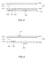
- FIG. 9 is the cross-sectional view of a sixth preferred embodiment of flat fluorescent lamp in accordance with the present invention.
- the flat fluorescent lamp comprises a dielectric substrate 600a, an upper substrate 600b, a fluorescent substance 602, a discharge gas 604 and a plurality of first and second electrodes 606, 607.
- the dielectric substrate 600a and the upper substrate 600b are arranged in parallel and therefore a gas discharge chamber 600 is formed therebetween.
- the gas discharge chamber 600 is filled with the discharge gas 604.
- the first electrode 606 is disposed on the outer surface of the dielectric substrate 600a.
- the second electrode 607 is disposed on the inner surface of the dielectric substrate 500a and is covered with a dielectric layer 609.
- the flat fluorescent lamp shown in the FIG. 9 further comprises a third electrode 611 disposed on the upper substrate 600b.
- the third electrode 611 can be disposed on the outer surface of the upper substrate 600b.
- the third electrode 611 covered with a dielectric layer like the dielectric layer 609 can be disposed on the inner surface of the upper substrate 600b.
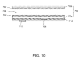
- FIG. 10 is the cross-sectional view of a seventh preferred embodiment of flat fluorescent lamp in accordance with the present invention.
- the flat fluorescent lamp comprises a dielectric substrate 700a, an upper substrate 700b, a fluorescent substance 702, a discharge gas 704 and a plurality of first and second electrodes 706, 712.
- the dielectric substrate 700a and the upper substrate 700b are arranged in parallel and therefore a gas discharge chamber 700 is formed therebetween.
- the gas discharge chamber 700 is filled with the discharge gas 704.
- the flat fluorescent lamp further comprises a reflective layer 718 beneath the dielectric substrate 700a so that the first electrode 706 is disposed between the dielectric substrate 700a and the reflective layer 718.
- the second electrode 712 can be disposed on the outer surface of the reflective layer 700a.
- the first and second electrodes 706,712 are linear, strip, zigzag or other type.
- the second electrode 712 is parallel or perpendicular to the first electrode 706.
- the second electrode 712 can also be planar.
- the arrangement of the electrode pairs shown in FIG. 10 is (ABAB) n .
- the arrangement of the electrode pairs can be (ABBA) n , (AAB) n , or (BBA) n .
- the dielectric substrates 300a, 400a, 500a, 600a, 700a are dielectric material such as glass or ceramic and have a thickness of about 0.3-2 mm; the upper substrates 300b, 400b, 500b, 600b, 700b are transparent material such as glass and have a thickness of about 0.3-5 mm; electrodes 306, 307, 406, 407, 506, 507, 606, 607, 611, 706, 712 are conductive material, such as silver, copper, ITO or IZO, having a thickness of 3-50 ⁇ m; the fluorescent substance 302, 402, 502, 602, 702 can be excited by the UV light to produce visible light and have a thickness of about 2-400 ⁇ m; the discharge gas 304, 404, 504, 604, 704 includes Xe, Ne, Ar, other insert gas, mercury free gas, or a mixture thereof; the dielectric layers 309, 409, 509, 609 are made of PbO, SiO 2 , Bi 2 O 3 , ceramic or combinations
- the edges of the upper substrate and the dielectric substrates can be connected with each other or connected by strips to form the gas discharge chambers 300, 400, 500, 600, 700.
- the distance between the dielectric substrate and the upper substrate is about 0.5-10 mm.
- At least one spacer can be optionally mounted between the dielectric substrate and the upper substrate to maintain the distance.
- the electrode pair including the first and the second electrodes is disposed on the different planes.
- the flat fluorescent lamp of this invention can produce a larger discharge area to perform a better efficiency of luminance.
- the cost of dielectric material could be reduced to a half of conventional design.
Landscapes
- Physics & Mathematics (AREA)
- Engineering & Computer Science (AREA)
- Plasma & Fusion (AREA)
- Electromagnetism (AREA)
- Vessels And Coating Films For Discharge Lamps (AREA)
Abstract
Description
- The present invention relates to a flat lamp structure having electrodes positioned on the outer wall of a gas discharge chamber, and in particular, to a flat fluorescent lamp having electrodes disposed on different planes.
- As a consequence of industrial progress, developments in mobile phones, digital cameras, digital video cameras, notebook computers, and desk-top computers are now concerned with multifunctional and aesthetic design. However, the display screen used in mobile phones, digital cameras, digital video cameras, notebook computers, and desk-top computers is an essential interactive interface. The display screen provides the user with great convenience of operation. In recent years, it has become commonplace for most mobile phones, digital cameras, digital video cameras, notebook computers, and desk-top computers to employ a LCD panel as the display screen. However, the LCD panel per se is non-luminous, and a back light module must be provided at the bottom of the LCD panel to provide a light source for displaying.
- The flat lamp provides excellent luminosity and uniformity and also provides a larger surface area light source. Therefore, it is widely applied as a back light source for LCD panels and for other fields of applications. The flat lamp is a plasma luminous component, essentially utilizing the electrons emitted from the cathode to collide with the inert gas between the cathode and anode within the gas discharge chamber, and the gas is ionized and excited to form plasma. After that the excited state atoms of the plasma return to the ground state by emission of UV rays, the UV rays further excite the fluorescence substance within the flat lamp, producing visible light.
- FIG. 1 is a schematic view showing the structure of a conventional flat lamp.
- Referring to FIG. 1, the conventional flat lamp structure comprises a
gas discharge chamber 100, afluorescence substance 102, adischarge gas 104,electrodes 106 anddielectric layers 108. Thegas discharge chamber 100 comprises aplate 100a, asecond plate 100b andstrip 100c mounted between theplate 100a and theplate 100b, and is connected to the edge of theplate 100a and the edge ofplate 100b to form a closed chamber. - Referring again to FIG. 1, the
conventional electrode 106 is generally a silver electrode, and theelectrode 106 is disposed on theplate 100a. The electrode is generally covered with thedielectric layer 108 so as to protect theelectrode 106 from damaging by the collision of the ions. As shown in FIG. 1, thedielectric layer 108 coveringelectrode 106 is positioned at the inner wall of thegas discharge chamber 100. Thegas discharge chamber 100 is charged with agas 104. Generally, thegas 104 includes Xe, Ne and Ar, or other inert gas. Moreover, thefluorescence substance 102 is disposed on the inner wall of thegas discharge chamber 100, for example on the surface of theplate 100b, on the surface of thedielectric layer 108, and on the surface of theplate 100a not covered by thedielectric layer 108. - In the process of ignition of the flat lamp, the
electrode 106 emits electrons to collide with thedischarge gas 104 within thegas discharge chamber 100, and thedischarge gas 104 is ionized and excited to form plasma. After that, the excited state atoms of the plasma return to the ground state by emitting UV rays, and the emitted UV rays further excite thefluorescence substance 102 within the inner wall of thegas discharge chamber 100 to produce visible light. However, on the above light luminous mechanism, the high energy ions released by the plasma generally collide through the dielectric layer, and may reach further to theelectrode 106. Thus, the longevity of the flat lamp is greatly reduced. - Please note that the
dielectric layer 108 covering theelectrode 106 is generally fabricated by a multiple screen printing process the thickness of which is controlled between 200 µm to 250 µm. However, the fabrication process of the multiple screen printing is complicated, and the test sample capacity and yield are low. In addition, multiple screen printing can easily cause unevenness in the thickness of the film, causing each of the test samples or a single test sample with different optical characteristics of different region to differ with each other. Due to the fact that the optical characteristics of the test sample cannot be easily controlled, the designing cost for the driving circuit is increased. - Accordingly, it is an object of the present invention to provide a flat lamp structure which effectively avoids collision through the dielectric layer, improving the longevity of the flat lamp.
- Another object of the present invention is to provide a flat lamp structure which effectively avoids the unevenness occurring on the dielectric substrate film due to multiple screen printing, thereby improving the luminosity and the uniformity of the flat lamp.
- In order to achieve the above objects, the present invention provides a flat lamp structure comprising a gas discharge chamber; a fluorescence substance disposed on the inner wall of the gas discharge chamber; a discharge gas disposed in the gas discharge chamber; and a plurality of electrodes disposed on the outer wall of the gas discharge chamber.
- The gas discharge chamber, for example, comprises a dielectric substrate; a plate disposed on the upper portion of the dielectric substrate; and a plurality of strips disposed between the dielectric substrate and the plate, and the plate connected to the edge of the dielectric substrate.
- In order to achieve the above objects, the present invention provides a flat lamp structure comprising a gas discharge chamber; a fluorescence substance disposed on the inner wall of the gas discharge chamber; a discharge gas disposed in the gas discharge chamber; a plurality of electrodes disposed on the outer wall of the gas discharge chamber; and a spacer disposed on the gas discharge chamber to enhance the strength of the gas discharge chamber.
- The gas discharge chamber, for example, comprises a dielectric substrate; a plate disposed on the upper portion of the dielectric substrate; and a plurality of strips disposed between the dielectric substrate and the plate, and plate connected to the edge of the dielectric substrate.
- In accordance with a preferred embodiment of the present invention, the thickness of the dielectric substrate is, for example, between 0.3 mm and 1.1 mm, and the distance between the dielectric substrate and the plate, for example, is between 0.5 mm and 2.0 mm.
- In accordance with the preferred embodiment of the present invention, the gas charged into the gas discharge chamber, for example, is Xe, Ne or Ar, and the electrodes, for example, include silver electrode or copper electrode.
- In accordance with the preferred embodiment of the present invention, the lower portion of the dielectric substrate, for example, is stuck to a carrier substrate for carrying the gas discharge chamber containing the electrode.
- In addition, an adhesive, for example, is disposed between the dielectric substrate and the carrier substrate and connects the dielectric substrate and the carrier substrate.
- In accordance with the preferred embodiment of the present invention, the adhesive, for example, includes glass adhesive, UV curing adhesive or thermal curing adhesive.
- In accordance with the present invention, the electrode is fabricated on the outer wall of the gas discharge chamber, and by means of the dielectric substrate as dielectric material for protecting the electrode, the uniformity with respect to thickness is good and the ability to withstand the collision of ions is excellent. Thus, the present invention does not require a dielectric layer formed by multiple screen printing covering the electrode, resulting in uniformity of luminosity and significant improvement in longevity.
- Furthermore, in order to improve the longevity and efficiency of luminance, the flat fluorescent lamp of the present invention comprises at least an electrode pair formed by one first electrode and one second electrode on different planes.
- In accordance with a preferred embodiment of the present invention, the first electrode is disposed on the outer surface of the dielectric substrate and the second electrode covered with a dielectric layer is disposed on the inner surface of the dielectric substrate.
- In accordance with a preferred embodiment of the present invention, the first electrode is disposed on the outer surface of the dielectric substrate without covering the dielectric layer and the second electrode covered with the dielectric layer is disposed on the inner surface of the dielectric substrate. The first and second electrodes are both strip type and are perpendicular each other. Also, the first electrode could be planar type.
- In accordance with a preferred embodiment of the present invention, the flat fluorescent lamp further comprises a carrier substrate beneath the dielectric substrate for supporting the flat fluorescent lamp. The first electrode is disposed on the outer surface of the dielectric substrate or is disposed on one surface of the carrier substrate facing the dielectric substrate. The second electrode covered with the dielectric layer is disposed on the inner surface of the dielectric substrate. An adhesive is disposed between the dielectric substrate and the carrier substrate for connecting the two substrates.
- In accordance with a preferred embodiment of the present invention, the flat fluorescent lamp further comprises a third electrode disposed on the outer surface of the upper plate, or covered with the dielectric layer on the inner surface of the upper plate.
- In accordance with a preferred embodiment of the present invention, the flat fluorescent lamp further comprises a reflective layer disposed beneath the dielectric substrate so that the first electrode is disposed between the dielectric substrate and the reflective layer. Based on the concept of the present invention, the second electrode is disposed on the outer surface of the reflective layer.
- Based on the concept of the present invention, the electrode pair, including the first and the second electrodes, is disposed on the different planes so that the discharge area between the two electrodes is larger than that between two electrodes on the same plane in general. Thus, the flat fluorescent lamp of the present invention provides significant improvement in luminosity.
-
- FIG. 1 is a schematic view of a conventional flat lamp structure;
- FIGS. 2 and 3 are schematic views of a first preferred embodiment flat lamp in accordance with the present invention;
- FIGS. 4 and 5 are schematic views of a second preferred embodiment flat lamp in accordance with the present invention;
- FIG. 6 is a cross-sectional view of a third preferred embodiment of the flat fluorescent lamp in accordance with the present invention;
- FIG. 7A is a cross-sectional view of a fourth preferred embodiment of the flat fluorescent lamp in accordance with the present invention;
- FIGS. 7B and 7C are schematic views of the modifications of the dielectric substrate of the fourth preferred embodiment of the flat fluorescent lamp in accordance with the present invention;
- FIG. 8 is a cross-sectional view of a fifth preferred embodiment of the flat fluorescent lamp in accordance with the present invention;
- FIG. 9 is a cross-sectional view of a sixth preferred embodiment of the flat fluorescent lamp in accordance with the present invention; and
- FIG. 10 is a cross-sectional view of a seventh preferred embodiment of the flat fluorescent lamp in accordance with the present invention.
- Reference will now be made in detail to the present preferred embodiments of the invention, examples of which are illustrated in the accompanying drawings. Wherever possible, the same reference numbers are used in the drawings and the description to refer to the same or like parts.
- In the embodiments illustrated in the descriptions, the "inner surface" of the upper plate or the dielectric substrate indicated the surface facing the gas discharge chamber, and the "outer surface" of the upper plate or the dielectric substrate is the opposite side of the "inner surface", respectively.
- FIGS. 2 and 3 show schematically the flat lamp structure of a first preferred embodiment of the present invention.
- First, referring to FIG. 2, the flat lamp comprises a
gas discharge chamber 200,fluorescence substance 202, adischarge gas 204 and a plurality ofelectrodes 206. Wherein the material for forming the gas discharge chamber is, for example, glass. Thegas discharge chamber 200, for instance, is adielectric substrate 200a, aplate 200b and a plurality ofstrips 200c. Theplate 200b is disposed on the upper portion of thedielectric substrate 200a, and thestrips 200c are disposed between thedielectric substrate 200a and theplate 200b, and are connected to thedielectric substrate 200a and the edge of theplate 200b. In the present preferred embodiment, the thickness of the dielectric substrate is, for example, between 0.3 mm to 1.1 mm, and the distance between thedielectric substrate 200a and theplate 200b is, for example, between 0.5 mm and 2.0 mm. - Similarly, referring to FIG. 2, the
fluorescence substance 202 is disposed on the inner wall of the gas dischargedchamber 200, and thefluorescence substance 202 is generally disposed on thedielectric substrate 200a and the surface of theplate 200b. Thegas 204 is charged into thegas discharge chamber 200, and examples of the gas are Xe, Ne, and Ar. Theelectrode 206 is disposed on the outer wall of thegas discharge chamber 200. Examples of the electrodes are silver electrode or copper electrode. - In the process of ignition of the flat lamp, the
electrode 206 on the outer wall of thegas discharge chamber 200 is driven so that the electrode within thegas discharge chamber 202 partially emits electrons which collide with thegas 204, and thegas 204 is ionized and excited to form plasma. After that, the excited state atoms of the plasma return to the ground state by way of emission of UV rays, and the emitted UV rays further excite thefluorescence substance 202 on the inner wall of thegas discharge chamber 200 so as to produce visible light. - In accordance with the preferred embodiment during the driving process, the
electrodes 206, isolated by thedielectric substrate 200a, form an electric field within thegas discharge chamber 200, and the thickness of thedielectric substrate 200a directly affects the difficulty of the driving process. When the thickness of thedielectric substrate 200a is large, the flat lamp is more difficult to drive, and vice versa; to facilitate the driving process, a thinnerdielectric material 200a is used. In contrast, thedielectric substrate 200a may be broken for the reason that thesubstrate 200a cannot withstand the external atmospheric pressure. Thus, in order to consider both the difficulty of the driving process and the strength of thedielectric substrate 200a, the present preferred embodiment provides a flat lamp structure, as shown in FIG. 3. - Referring to FIG. 3, in order to obtain a balance between the difficulty of the driving process and the strength of the
dielectric substrate 200a, the present flat lamp structure, as shown in FIG. 2, is supported on acarrier substrate 210, and thedielectric substrate 200a and thecarrier substrate 210 are connected, for example, by means of an adhesive 208 having a thickness between 0.1 mm and 0.3 mm. In accordance with the present invention, the adhesive 208 includes, for example, glass adhesive, UV curing adhesive or thermal curing adhesive. - In accordance with the flat lamp structure, as the
dielectric substrate 200a and thecarrier substrate 210 are connected using the adhesive 208, the structural body constructed by thedielectric substrate 200a and thecarrier substrate 210 can withstand the external atmospheric pressure, thus, as a whole, the strength of the flat lamp is enhanced. - FIGS. 4 and 5 show a flat lamp structure in accordance with the second preferred embodiment. As shown in FIG. 4, the flat lamp comprises a
gas discharge chamber 200, afluorescence substance 202, adischarge gas 204, a plurality ofelectrodes 206 and at least aspacer 300, wherein the material of thegas discharge chamber 200 is, for example, glass. Thegas discharge chamber 200 comprises adielectric substrate 200a, aplate 200b and a plurality ofstrips 200c. Theplate substrate 200b is disposed on the upper portion of thedielectric substrate 200a, and thestrips 200c are disposed between thedielectric substrate 200a and theplate 200b, and thedielectric substrate 200a and the edge of theplate 200b are connected. In accordance with the preferred embodiment, the thickness of thedielectric substrate 200a is, for example, between 0.3 mm and 1.1 mm, and the distance between thedielectric substrate 200a and theplate 200b is, for example, between 0.5 mm and 2.0 mm. - Similarly, referring to FIG. 4, the
fluorescence substance 202 is disposed on the inner wall of the gas disposedchamber 200, and thefluorescence substance 202 is generally disposed on thedielectric substrate 200a and the surface of theplate 200b. Thegas 204 is charged into thegas discharge chamber 200, and an example of the gas is Xe. Theelectrode 206 is disposed on the outer wall of thegas discharge chamber 200. An example of the electrode is silver electrode. - The flat lamp structure of the present invention is similar to that of the first preferred embodiment, and the only difference is on the design of the
spacer 300. - The
spacer 300 is designed out of concern for the difficulty of the driving process and the strength of thedielectric substrate 200a; thespacer 300 of thegas discharge chamber 200b can withstand thedielectric substrate 200a and the surface of theplate 200b such that the strength of thedielectric substrate 200a can be enhanced, and its breakage as a result of its inability to withstand the external atmospheric pressure will not occur. - Next, referring to FIG. 5, there is shown the flat lamp structure similar to that shown in FIG. 3, the only difference is on the design of the
spacer 300. In accordance with the present preferred embodiment, the dual reinforcement of thespacer 300 with the combination of thecarrier 210 deals with the difficulty of the driving process and the strength of thedielectric substrate 200a. - In accordance with the present invention, the dielectric substrate with controllable thickness and uniformity is used to substitute conventional dielectric layer formed from multiple screen printing process and the electrode is disposed on the outer wall of the gas discharge chamber to form external electrodes. Thus, the flat lamp structure of the present invention possesses the following advantages: (1) the replacement of the dielectric layer fabricated by multiple screen printing with the present dielectric substrate provides a simple fabrication process and the fabrication time is shortened, and the yield is improved; (2) the replacement of the dielectric layer fabricated by multiple screen printing with the present dielectric substrate alleviates the error in the fabrication process, thus improving yield and reducing production costs; and (3) excellent thickness uniformity of the dielectric substrate allows for a small difference of electric field between the individual electrodes, thus the uniformity of light emission of the flat lamp is improved.
- In order to improve the longevity and efficiency of luminance, the present invention provides another preferred embodiments of the flat fluorescent lamp comprising at least an electrode pair formed by one first electrode and one second electrode, both of which are positioned on different planes.
- FIG. 6 is the cross-sectional view of the third preferred embodiment of flat fluorescent lamp in accordance with the present invention.
- Referring to FIG. 6, the flat fluorescent lamp comprises a dielectric substrate 300a, an
upper substrate 300b, afluorescent substance 302, adischarge gas 304 and a plurality of first andsecond electrodes dielectric substrate 300b are arranged in parallel and therefore agas discharge chamber 300 is formed therebetween. Thegas discharge chamber 300 is filled with thedischarge gas 304. Thefirst electrode 306 is disposed on the outer surface of the dielectric substrate 300a without covering the dielectric layer. Thesecond electrode 307 is disposed on the inner surface of the dielectric substrate 300a and is covered with adielectric layer 309. Thefluorescent substance 302 is disposed on the inner surface of thegas discharge chamber 300. - In accordance with the flat fluorescent lamp shown in FIG. 6, the first and
second electrodes - Assuming the first and
second electrodes - FIG. 7A is a cross-sectional view of a fourth preferred embodiment of the flat fluorescent lamp in accordance with the present invention.
- As shown in FIG. 7A, the flat fluorescent lamp comprises a
dielectric substrate 400a, anupper substrate 400b, afluorescent substance 402, adischarge gas 404 and a plurality of first andsecond electrodes dielectric substrate 400a and theupper substrate 400b are arranged in parallel and therefore agas discharge chamber 400 is formed therebetween. Thegas discharge chamber 400 is filled with thedischarge gas 404. Thefirst electrode 406 is disposed on the outer surface of thedielectric substrate 400a. Thesecond electrode 407 is disposed on the inner surface of thedielectric substrate 400a and is covered with adielectric layer 409. Thefluorescent substance 402 is disposed on the inner surface of thegas discharge chamber 400. - FIGS. 7B and 7C are schematic views of the modifications of the dielectric substrate of the fourth preferred embodiment of the flat fluorescent lamp in accordance with the present invention
- In the flat fluorescent lamp shown in FIG. 7B, the
first electrode 406 is planar and the second electrode is linear. The second electrode can also be strip, zigzag or other types. - In the flat fluorescent lamp shown in FIG. 7C, the
first electrode 406 is linear and thesecond electrode 407 is linear and perpendicular to thefirst electrode 406. The first andsecond electrodes - FIG. 8 is the cross-sectional view of a fifth preferred embodiment of flat fluorescent lamp in accordance with the present invention.
- The flat fluorescent lamp shown in FIG. 4 comprises a
dielectric substrate 500a, anupper substrate 500b, afluorescent substance 502, adischarge gas 504 and a plurality of first andsecond electrodes dielectric substrate 500a and theupper substrate 500b are arranged in parallel and therefore agas discharge chamber 500 is formed therebetween. Thegas discharge chamber 500 is filled with thedischarge gas 504. Thesecond electrode 507 is disposed on the inner surface of thedielectric substrate 500a and is covered with adielectric layer 509. - The flat fluorescent lamp further comprises a
carrier substrate 510 disposed beneath thedielectric substrate 500a for supporting the flat fluorescent lamp. Thefirst electrode 506 is disposed on the outer surface of thedielectric substrate 500a or is disposed on one surface of thecarrier substrate 510 facing thedielectric substrate 500a. An adhesive 508, such as glass glue, ceramic glue, UV curing adhesive or thermal curing adhesive, is disposed between thedielectric substrate 500a and thecarrier substrate 510 for connecting thedielectric substrate 500a and thecarrier substrate 510. - Assuming the first and the
second electrodes dielectric substrate 500a are represented as "A" and "B", respectively, the arrangement of the electrode pairs shown in FIG. 8 is (ABAB)n. Based on the concept of the present invention, the arrangement of the electrode pairs can be (ABBA)n, (AAB)n, or (BBA)n. - FIG. 9 is the cross-sectional view of a sixth preferred embodiment of flat fluorescent lamp in accordance with the present invention.
- Referring to FIG. 9, the flat fluorescent lamp comprises a dielectric substrate 600a, an
upper substrate 600b, afluorescent substance 602, adischarge gas 604 and a plurality of first andsecond electrodes upper substrate 600b are arranged in parallel and therefore agas discharge chamber 600 is formed therebetween. Thegas discharge chamber 600 is filled with thedischarge gas 604. Thefirst electrode 606 is disposed on the outer surface of the dielectric substrate 600a. Thesecond electrode 607 is disposed on the inner surface of thedielectric substrate 500a and is covered with adielectric layer 609. - The flat fluorescent lamp shown in the FIG. 9 further comprises a
third electrode 611 disposed on theupper substrate 600b. Based on the concept of the present invention, thethird electrode 611 can be disposed on the outer surface of theupper substrate 600b. Optionally, thethird electrode 611 covered with a dielectric layer like thedielectric layer 609 can be disposed on the inner surface of theupper substrate 600b. - FIG. 10 is the cross-sectional view of a seventh preferred embodiment of flat fluorescent lamp in accordance with the present invention.
- As shown in the FIG. 10, the flat fluorescent lamp comprises a
dielectric substrate 700a, anupper substrate 700b, afluorescent substance 702, adischarge gas 704 and a plurality of first andsecond electrodes dielectric substrate 700a and theupper substrate 700b are arranged in parallel and therefore agas discharge chamber 700 is formed therebetween. Thegas discharge chamber 700 is filled with thedischarge gas 704. The flat fluorescent lamp further comprises areflective layer 718 beneath thedielectric substrate 700a so that thefirst electrode 706 is disposed between thedielectric substrate 700a and thereflective layer 718. Thesecond electrode 712 can be disposed on the outer surface of thereflective layer 700a. - In the embodiments of the present invention, the first and second electrodes 706,712 are linear, strip, zigzag or other type. The
second electrode 712 is parallel or perpendicular to thefirst electrode 706. Thesecond electrode 712 can also be planar. - Assuming the electrode pair, i.e. the first and
second electrodes - In the embodiments shown in FIGS. 6 to 10, the dielectric substrates 300a, 400a, 500a, 600a, 700a are dielectric material such as glass or ceramic and have a thickness of about 0.3-2 mm; the upper substrates 300b, 400b, 500b, 600b, 700b are transparent material such as glass and have a thickness of about 0.3-5 mm; electrodes 306, 307, 406, 407, 506, 507, 606, 607, 611, 706, 712 are conductive material, such as silver, copper, ITO or IZO, having a thickness of 3-50µm; the fluorescent substance 302, 402, 502, 602, 702 can be excited by the UV light to produce visible light and have a thickness of about 2-400µm; the discharge gas 304, 404, 504, 604, 704 includes Xe, Ne, Ar, other insert gas, mercury free gas, or a mixture thereof; the dielectric layers 309, 409, 509, 609 are made of PbO, SiO2, Bi2O3, ceramic or combinations thereof and have a thickness of about 30-400µm; the carrier substrate 510 is glass or ceramic; the adhesive 508 is glass glue, ceramic glue, UV curing adhesive or thermal curing adhesive; and the reflective layer 718 is made of glass material doped with TiO2, Al2O3 or combinations thereof.
- As the embodiments illustrated in the present invention, the edges of the upper substrate and the dielectric substrates can be connected with each other or connected by strips to form the
gas discharge chambers - In accordance with the flat fluorescent lamps in the all embodiments of the present invention, the electrode pair including the first and the second electrodes is disposed on the different planes. In comparison with the conventional flat lamp, the flat fluorescent lamp of this invention can produce a larger discharge area to perform a better efficiency of luminance. Furthermore, in comparison with the conventional flat lamp, the cost of dielectric material could be reduced to a half of conventional design.
- While there has been shown and described what are at the present considered the preferred embodiments of the invention, it will be obvious to those skilled in the art that various changes and modifications may be made therein without departing from the scope of the invention as defined by the appended claims.
Claims (28)
- A flat fluorescent lamp comprising:a gas discharge chamber formed between a first substrate and a second substrate and filled with a discharge gas;a fluorescent substance disposed on an inner surface of the gas discharge chamber; andat least one electrode pair including a first electrode and a second electrode;wherein the first and second electrodes are disposed on opposite surfaces of the first substrate, or the first and second electrodes are disposed on the same side of the first substrate but positioned on a different plane.
- The flat fluorescent lamp as claimed in claim 1, further comprising at least one spacer mounted between the first and second substrates to maintain a distance.
- The flat fluorescent lamp as claimed in claim 1 or 2, wherein the second electrode is disposed on an inner surface of the first substrate and is covered with a dielectric layer.
- The flat fluorescent lamp as claimed in claim any of the preceding claims, wherein the dielectric layer is made of PbO, SiO2, Bi2O3, ceramic or combinations thereof and has a thickness at about 30-400µm.
- The flat fluorescent lamp as claimed in any of the preceding claims, wherein the first or second substrate is linear, strip, zigzag, wave or plane type.
- The flat fluorescent lamp as claimed in claim 5, wherein the second electrode is arranged in parallel or perpendicular to the first electrode.
- The flat fluorescent lamp as claimed in any of the preceding claims, further comprises a carrier substrate beneath the first substrate.
- The flat fluorescent lamp as claimed in claim 7, wherein the carrier substrate is glass or ceramic.
- The flat fluorescent lamp as claimed in claim 7 or 8, further comprising an adhesive disposed between the first substrate and the carrier substrate to connect thereof.
- The flat fluorescent lamp as claimed in claim 9, wherein the adhesive comprises glass glue, ceramic glue, UV curing adhesive or thermal curing adhesive.
- The flat fluorescent lamp as claimed in any of claims 2 to 10, further comprising a third electrode disposed on the second substrate.
- The flat fluorescent lamp as claimed in any of the preceding claims, further comprising a reflective layer beneath the first substrate so that the first electrode is deposed between the first substrate and the reflective layer.
- The flat fluorescent lamp as claimed in claim 12, wherein the reflective layer is made of a glass material doped with TiO2, Al2O3 or combinations thereof.
- The flat fluorescent lamp as claimed in claim 12 or 13, wherein the second electrode is disposed on a surface of the reflective layer.
- The flat fluorescent lamp as claimed in any of the preceding claims, wherein the first and second substrates are a dielectric material, glass or ceramic, and have a thickness of about 0.3-5 mm.
- The flat fluorescent lamp as claimed in any of claims 1 to 14, wherein the first and second electrodes are formed by a conductive material, metal, silver, copper, ITO or IZO and have a thickness of 3-50µm, respectively.
- The flat fluorescent lamp as claimed in any of the preceding claims, wherein the fluorescent substance is excited by a UV light to produce visible light and has a thickness of about 2-400µm.
- The flat fluorescent lamp as claimed in any of the preceding claims, wherein the discharge gas comprises Xe, Ne, Ar, insert gas, mercury-free gas, or a mixture thereof.
- The flat fluorescent lamp as claimed in any of the preceding claims, wherein the first and second electrodes are represented as "A" and "B", respectively, and the arrangement of the first and second electrodes is (ABAB)n, (ABBA)n, (AAB)n or (BBA) n.
- A flat fluorescent lamp comprising:a gas discharge chamber comprising
a dielectric substrate, and
a substrate disposed on the upper portion of the dielectric substrate;a fluorescence substance disposed on the inner surface of the gas discharge chamber;a discharge gas disposed in the gas discharge chamber; anda plurality of electrodes disposed on the outer surface of the gas discharge chamber;wherein a distance between the dielectric substrate and the substrate is between 0.5 mm to 10 mm. - The flat fluorescent lamp as claimed in claim 20, further comprising at least one spacer mounted between the dielectric substrate and the substrate to maintain the distance.
- The flat fluorescent lamp as claimed in claim 20 or 21, wherein the gas discharge chamber further comprises:a plurality of strips disposed between the dielectric substrate and the substrate connected to the edge of the dielectric substrate.
- The flat fluorescent lamp as claimed in any of claims 20 or 22, wherein the thickness of the dielectric substrate is ranged from 0.3 mm to 2 mm.
- The flat fluorescent lamp as claimed in any of claims 20 to 23, wherein the discharge gas comprises Xe, Ne, Ar, inert gas, mercury-free gas, or a mixture thereof.
- The flat fluorescent lamp as claimed in any of claims 20 to 24, wherein the electrode is made of silver, copper, metal, ITO, IZO or a conductive material.
- The flat fluorescent lamp as claimed in any of claims 20 to 25, further comprising a carrier substrate disposed beneath the dielectric substrate to carry the gas discharge chamber.
- The flat fluorescent lamp as claimed in claim 26, further comprising an adhesive disposed between the dielectric substrate and the carrier substrate, said adhesive connecting the dielectric substrate and the carrier substrate.
- The flat fluorescent lamp as claimed in claim 27, wherein the adhesive includes a ceramic glue, glass adhesive, UV curing adhesive or thermal curing adhesive.
Priority Applications (2)
| Application Number | Priority Date | Filing Date | Title |
|---|---|---|---|
| EP06122921A EP1916698A1 (en) | 2006-10-25 | 2006-10-25 | Flat fluorescent lamp |
| TW96107616A TW200820304A (en) | 2006-10-25 | 2007-03-06 | Flat fluorescent lamp |
Applications Claiming Priority (1)
| Application Number | Priority Date | Filing Date | Title |
|---|---|---|---|
| EP06122921A EP1916698A1 (en) | 2006-10-25 | 2006-10-25 | Flat fluorescent lamp |
Publications (1)
| Publication Number | Publication Date |
|---|---|
| EP1916698A1 true EP1916698A1 (en) | 2008-04-30 |
Family
ID=37847287
Family Applications (1)
| Application Number | Title | Priority Date | Filing Date |
|---|---|---|---|
| EP06122921A Withdrawn EP1916698A1 (en) | 2006-10-25 | 2006-10-25 | Flat fluorescent lamp |
Country Status (2)
| Country | Link |
|---|---|
| EP (1) | EP1916698A1 (en) |
| TW (1) | TW200820304A (en) |
Cited By (1)
| Publication number | Priority date | Publication date | Assignee | Title |
|---|---|---|---|---|
| JP2019061759A (en) * | 2017-09-25 | 2019-04-18 | 株式会社Screenホールディングス | Plasma generating device and electrode body for plasma generation |
Families Citing this family (1)
| Publication number | Priority date | Publication date | Assignee | Title |
|---|---|---|---|---|
| JPWO2009145200A1 (en) * | 2008-05-30 | 2011-10-13 | 旭硝子株式会社 | Fluorescent lamp |
Citations (4)
| Publication number | Priority date | Publication date | Assignee | Title |
|---|---|---|---|---|
| DE19952242A1 (en) * | 1999-10-29 | 2001-05-03 | Philips Corp Intellectual Pty | Plasma screen used e.g. for military applications comprises support plate, transparent front plate, ribbed structure, electrode arrays and phosphor layer made of a rare earth metal borate |
| EP1519406A1 (en) * | 2003-07-31 | 2005-03-30 | Delta Optoelectronics, Inc. | Flat lamp structure |
| US20050116607A1 (en) * | 2003-11-29 | 2005-06-02 | Park Deuk-Il | Flat fluorescent lamp and backlight unit using the same |
| EP1615256A1 (en) * | 2004-07-08 | 2006-01-11 | Samsung Corning Co., Ltd. | Flat lamp |
-
2006
- 2006-10-25 EP EP06122921A patent/EP1916698A1/en not_active Withdrawn
-
2007
- 2007-03-06 TW TW96107616A patent/TW200820304A/en unknown
Patent Citations (4)
| Publication number | Priority date | Publication date | Assignee | Title |
|---|---|---|---|---|
| DE19952242A1 (en) * | 1999-10-29 | 2001-05-03 | Philips Corp Intellectual Pty | Plasma screen used e.g. for military applications comprises support plate, transparent front plate, ribbed structure, electrode arrays and phosphor layer made of a rare earth metal borate |
| EP1519406A1 (en) * | 2003-07-31 | 2005-03-30 | Delta Optoelectronics, Inc. | Flat lamp structure |
| US20050116607A1 (en) * | 2003-11-29 | 2005-06-02 | Park Deuk-Il | Flat fluorescent lamp and backlight unit using the same |
| EP1615256A1 (en) * | 2004-07-08 | 2006-01-11 | Samsung Corning Co., Ltd. | Flat lamp |
Non-Patent Citations (1)
| Title |
|---|
| JEONGWOOK HUR ET AL: "43.3: Flat Panel Light Source and High Power Inverter for LCD Backlight Application", SID 00 DIGEST, 2000 SID INTERNATIONAL SYMPOSIUM, MAY 16-18 2000, LONG BEACH (CA), vol. XXXI, 2000, pages 1033 - 1035, XP007007466 * |
Cited By (1)
| Publication number | Priority date | Publication date | Assignee | Title |
|---|---|---|---|---|
| JP2019061759A (en) * | 2017-09-25 | 2019-04-18 | 株式会社Screenホールディングス | Plasma generating device and electrode body for plasma generation |
Also Published As
| Publication number | Publication date |
|---|---|
| TW200820304A (en) | 2008-05-01 |
Similar Documents
| Publication | Publication Date | Title |
|---|---|---|
| US20030132711A1 (en) | Flat type lamp and liquid crystal display apparatus having the same | |
| US6744195B2 (en) | Flat luminescence lamp | |
| US20060006805A1 (en) | Flat lamp | |
| US7148626B2 (en) | Flat lamp structure with electrodes disposed on outer surface of the substrate | |
| US7078857B2 (en) | Flat luminescent lamp and method for manufacturing the same | |
| US20070040508A1 (en) | Flat fluorescent lamp | |
| US7294957B2 (en) | Flat lamp | |
| US20050280347A1 (en) | Flat lamp | |
| US20050035712A1 (en) | Cold cathode fluorescent flat lamp | |
| EP1519406A1 (en) | Flat lamp structure | |
| US7250716B2 (en) | Cold cathode flat fluorescent lamp and patterned electrode thereof | |
| US20060267919A1 (en) | Backlight unit having surface luminescence structure | |
| CN100555041C (en) | Surface light source unit and liquid crystal display device having same | |
| KR100760934B1 (en) | Surface emitting lamp and manufacturing method thereof | |
| US20060038507A1 (en) | Flat lamp having photocatalytic layer | |
| US7492084B2 (en) | Flat-type fluorescent lamp including a discharge space and an electrode part including electron-transporting and electron-emitting electrodes method of manufacturing the same and display apparatus having the same | |
| KR100674100B1 (en) | AC Driven Plasma Element for Flat Lamps and Manufacturing Method Thereof | |
| JP2008108693A (en) | Flat fluorescent lamp | |
| CN1295742C (en) | Flat light structure | |
| CN101137256A (en) | Surface light source device with secondary electron emission layer, manufacturing method, and backlight unit | |
| US20060290281A1 (en) | Cold cathode fluorescent lamp module | |
| TW200820304A (en) | Flat fluorescent lamp | |
| KR100670204B1 (en) | Surface emitting lamp to improve brightness and uniformity of brightness | |
| KR100614119B1 (en) | AC Driven Plasma Element for Flat Lamps and Manufacturing Method Thereof | |
| CN101640162A (en) | Electrode structure for flat lamp |
Legal Events
| Date | Code | Title | Description |
|---|---|---|---|
| PUAI | Public reference made under article 153(3) epc to a published international application that has entered the european phase |
Free format text: ORIGINAL CODE: 0009012 |
|
| 17P | Request for examination filed |
Effective date: 20061030 |
|
| AK | Designated contracting states |
Kind code of ref document: A1 Designated state(s): AT BE BG CH CY CZ DE DK EE ES FI FR GB GR HU IE IS IT LI LT LU LV MC NL PL PT RO SE SI SK TR |
|
| AX | Request for extension of the european patent |
Extension state: AL BA HR MK RS |
|
| AKX | Designation fees paid |
Designated state(s): AT BE BG CH CY CZ DE DK EE ES FI FR GB GR HU IE IS IT LI LT LU LV MC NL PL PT RO SE SI SK TR |
|
| STAA | Information on the status of an ep patent application or granted ep patent |
Free format text: STATUS: THE APPLICATION IS DEEMED TO BE WITHDRAWN |
|
| 18D | Application deemed to be withdrawn |
Effective date: 20081031 |