EP1916505A1 - Photoelectric encoder, scale and method of manufacturing scale - Google Patents
Photoelectric encoder, scale and method of manufacturing scale Download PDFInfo
- Publication number
- EP1916505A1 EP1916505A1 EP07020944A EP07020944A EP1916505A1 EP 1916505 A1 EP1916505 A1 EP 1916505A1 EP 07020944 A EP07020944 A EP 07020944A EP 07020944 A EP07020944 A EP 07020944A EP 1916505 A1 EP1916505 A1 EP 1916505A1
- Authority
- EP
- European Patent Office
- Prior art keywords
- scale
- light
- reflection portions
- photoelectric encoder
- substrate
- Prior art date
- Legal status (The legal status is an assumption and is not a legal conclusion. Google has not performed a legal analysis and makes no representation as to the accuracy of the status listed.)
- Granted
Links
- 238000004519 manufacturing process Methods 0.000 title claims description 47
- 239000000758 substrate Substances 0.000 claims description 58
- 238000000034 method Methods 0.000 claims description 9
- 239000012780 transparent material Substances 0.000 claims description 6
- 230000001678 irradiating effect Effects 0.000 claims description 3
- 238000010586 diagram Methods 0.000 description 34
- 239000011295 pitch Substances 0.000 description 16
- VYZAMTAEIAYCRO-UHFFFAOYSA-N Chromium Chemical compound [Cr] VYZAMTAEIAYCRO-UHFFFAOYSA-N 0.000 description 12
- 229910052804 chromium Inorganic materials 0.000 description 12
- 239000011651 chromium Substances 0.000 description 12
- 230000000694 effects Effects 0.000 description 8
- 230000003287 optical effect Effects 0.000 description 8
- 238000005259 measurement Methods 0.000 description 7
- 238000006073 displacement reaction Methods 0.000 description 4
- 238000005530 etching Methods 0.000 description 4
- 230000014509 gene expression Effects 0.000 description 4
- 230000015572 biosynthetic process Effects 0.000 description 3
- 239000000463 material Substances 0.000 description 3
- 229910001220 stainless steel Inorganic materials 0.000 description 3
- 239000010935 stainless steel Substances 0.000 description 3
- 238000010521 absorption reaction Methods 0.000 description 2
- 230000008901 benefit Effects 0.000 description 2
- 238000005728 strengthening Methods 0.000 description 2
- 238000007740 vapor deposition Methods 0.000 description 2
- RTAQQCXQSZGOHL-UHFFFAOYSA-N Titanium Chemical compound [Ti] RTAQQCXQSZGOHL-UHFFFAOYSA-N 0.000 description 1
- 229910009372 YVO4 Inorganic materials 0.000 description 1
- 238000006243 chemical reaction Methods 0.000 description 1
- 230000000295 complement effect Effects 0.000 description 1
- 238000005260 corrosion Methods 0.000 description 1
- 230000007797 corrosion Effects 0.000 description 1
- 229910044991 metal oxide Inorganic materials 0.000 description 1
- 150000004706 metal oxides Chemical class 0.000 description 1
- 238000005498 polishing Methods 0.000 description 1
- 239000004065 semiconductor Substances 0.000 description 1
- 239000000126 substance Substances 0.000 description 1
- 229910052719 titanium Inorganic materials 0.000 description 1
- 239000010936 titanium Substances 0.000 description 1
- LSGOVYNHVSXFFJ-UHFFFAOYSA-N vanadate(3-) Chemical compound [O-][V]([O-])([O-])=O LSGOVYNHVSXFFJ-UHFFFAOYSA-N 0.000 description 1
- 229910052727 yttrium Inorganic materials 0.000 description 1
- VWQVUPCCIRVNHF-UHFFFAOYSA-N yttrium atom Chemical compound [Y] VWQVUPCCIRVNHF-UHFFFAOYSA-N 0.000 description 1
Images









Classifications
-
- G—PHYSICS
- G01—MEASURING; TESTING
- G01D—MEASURING NOT SPECIALLY ADAPTED FOR A SPECIFIC VARIABLE; ARRANGEMENTS FOR MEASURING TWO OR MORE VARIABLES NOT COVERED IN A SINGLE OTHER SUBCLASS; TARIFF METERING APPARATUS; MEASURING OR TESTING NOT OTHERWISE PROVIDED FOR
- G01D5/00—Mechanical means for transferring the output of a sensing member; Means for converting the output of a sensing member to another variable where the form or nature of the sensing member does not constrain the means for converting; Transducers not specially adapted for a specific variable
- G01D5/26—Mechanical means for transferring the output of a sensing member; Means for converting the output of a sensing member to another variable where the form or nature of the sensing member does not constrain the means for converting; Transducers not specially adapted for a specific variable characterised by optical transfer means, i.e. using infrared, visible, or ultraviolet light
- G01D5/32—Mechanical means for transferring the output of a sensing member; Means for converting the output of a sensing member to another variable where the form or nature of the sensing member does not constrain the means for converting; Transducers not specially adapted for a specific variable characterised by optical transfer means, i.e. using infrared, visible, or ultraviolet light with attenuation or whole or partial obturation of beams of light
- G01D5/34—Mechanical means for transferring the output of a sensing member; Means for converting the output of a sensing member to another variable where the form or nature of the sensing member does not constrain the means for converting; Transducers not specially adapted for a specific variable characterised by optical transfer means, i.e. using infrared, visible, or ultraviolet light with attenuation or whole or partial obturation of beams of light the beams of light being detected by photocells
- G01D5/347—Mechanical means for transferring the output of a sensing member; Means for converting the output of a sensing member to another variable where the form or nature of the sensing member does not constrain the means for converting; Transducers not specially adapted for a specific variable characterised by optical transfer means, i.e. using infrared, visible, or ultraviolet light with attenuation or whole or partial obturation of beams of light the beams of light being detected by photocells using displacement encoding scales
- G01D5/34707—Scales; Discs, e.g. fixation, fabrication, compensation
Definitions
- the present invention relates to a photoelectric encoder for use in precise measurement, a scale incorporated in the photoelectric encoder as an element, and a method of manufacturing the scale.
- a photoelectric encoder has been utilized in the art for precise measurement of linear displacement, angular displacement and the like.
- photoelectric encoders There are many types of photoelectric encoders.
- a photoreceiver in which a plurality of photodiodes are arranged in an array manner; a scale disposed so as to be allowed to move relative to the photoreceiver and in which a reflection type of phase grating is formed; and a light source that emits light to the phase grating (See Japanese Patent Application Publication No. 10-163549 ,for example).
- signal light reflected and generated at the phase grating of the scale is received by the photoreceiver so that an amount of displacement such as liner displacement is calculated using an electric signal generated by photoelectric conversion of the signal light.
- phase grating Since the signal light received by the photoreceiver is generated by the phase grating of the scale, the phase grating is an extremely important element of such a photoelectric encoder. Thus, it is desired means for easily manufacturing a phase grating with high precision.
- the grating of the scale may be formed with high density in order to achieve the phase grating with high precision, there is a problem that the costs of manufacturing the scale with high density are increased.
- an aspect of the present invention is directed to a photoelectric encoder.
- the photoelectric encoder of the present invention includes : a scale having a grating formed thereon along a measuring axis; a light source operative to emit light to the scale so as to form a light spot on the grating; and a photoreceiver operative to receive reflected light from the scale.
- the light source and the photoreceiver are disposed so as to be allowed to move relative to the scale at least in a direction along the measuring axis, and the light source emits the light to the scale so that the photoreceiver receives the reflected light by the scale.
- the light source emits light with different wavelengths
- the scale includes a plurality of reflection portions that respectively reflect the light with different wavelengths.
- the photoelectric encoder Since the photoelectric encoder has the configuration described above, the light source emits the light with different wavelengths so that light with one of the different wavelengths is reflected by one of the plurality of reflection portions. Therefore, the amount of information may be increased in accordance with the number of the different wavelengths included in the light reflected by the scale. The increase of the amount of information results in a photoelectric encoder with high precision. Such a photoelectric encoder can be manufactured at a low cost.
- the scale includes the plurality of reflection portions respectively having different depths from a surface of the scale so that each of the plurality of reflection portions reflects the light with one of the different wavelengths in accordance with the depth thereof.
- the plurality of reflection portions are respectively made of a plurality of color resists, and each of the plurality of color resists reflects or absorbs the light with one of the different wavelengths. Additionally or alternatively, it is preferable that in the plurality of reflection portions, diffraction gratings are respectively formed in incidence planes thereof, and each of the diffraction gratings diffracts light with a predetermined wavelength.
- the light source selectively emits light with at least two wavelengths. It is preferable that the photoelectric encoder further includes: a wavelength separator operative to separate the reflected light received by the photoreceiver on the basis of each of the different wavelengths, wherein the light source emits light with a predetermined wavelength range.
- the present invention is directed to a scale operative to reflect light emitted by a light source.
- the scale is allowed to move relative to the light source and a photoreceiver that are incorporated in a photoelectric encoder.
- the scale includes a plurality of reflection portions each of which reflects light with one of different wavelengths.
- the plurality of reflection portions respectively have different depths from a surface of the scale so that each of the plurality of reflection portions reflects the light with one of the different wavelengths in accordance with the depth thereof.
- the plurality of reflection portions are respectively made of a plurality of color resists, and each of the plurality of color resists reflects or absorbs the light with one of the different wavelengths. Additionally or alternatively, it is preferable that in the plurality of reflection portions, diffraction gratings are respectively formed in incidence planes thereof, and each of the diffraction gratings diffracts light with a predetermined wavelength.
- the present invention is directed to a method of manufacturing a scale for configuration of a photoelectric encoder.
- the method of the present invention includes: preparing a substrate; and forming a plurality of reflection portions in a surface of the substrate at predetermined pitch intervals, the plurality of reflection portions respectively reflecting light with different wavelengths.
- the forming the plurality of reflection portions includes forming the plurality of reflection portions respectively having different depths from a surface of the substrate in the surface of the substrate at the predetermined pitch intervals, and one of the plurality of reflection portions reflects light with one of different wavelengths in accordance with the depth thereof.
- the plurality of reflection portions are respectively made of a plurality of color resists, and each of the plurality of color resists reflects or absorbs the light with one of different wavelengths.
- the forming the plurality of reflection portions includes irradiating lasers respectively having different outputs to the substrate to oxidize the substrate so that each of the plurality of reflection portions has one of the different depths.
- the method further includes : after forming the plurality of reflection portions, forming a transparent material on surfaces of the plurality of reflection portions and the surface of the substrate.
- a photoelectric encoder with high precision in which the manufacturing cost is reduced, a scale incorporated in the photoelectric encoder as an element, and a method of manufacturing the scale for the photoelectric encoder can be provided.
- FIG. 1 is a schematic diagramthat shows the photoelectric encoder according to the first embodiment of the present invention.
- the photoelectric encoder of the first embodiment is configured from: a light source 1; a scale 2 provided with a phase grating 21 for reflecting light generated by the light source 1; a photoreceiver 3 subjected to the light reflected by the phase grating 21; and a control section 4 for controlling drive of the photoreceiver 3 and for deriving a measurement value from the light received by the photoreceiver 3.
- the control section 4 also controls On/Off of the light source 1.
- the light source 1 includes a red light-emitting diode (LED) 11 and a blue LED 12.
- the red LED 11 emits light with a center wavelength of 650nm
- the blue LED 12 emits light with a center wavelength of 388nm.
- the light source 1 includes an index scale 13a at a position where the red LED 11 and the blue LED 12 emit light thereto.
- the index scale 13a is provided on a long transparent substrate 13.
- An optical grid 131 is formed on a surface the transparent substrate 13, which is opposite to a surface that faces the red LED 11 and the blue LED 12.
- the optical grid 131 is configured from a plurality of light shield portions 131a that are arranged in a linear manner at predetermined pitch intervals (as one example of an array manner).
- the scale 2 is disposed so as to be spaced with a predetermined gap from the surface of the transparent substrate 13 that is opposite to the surface on which the optical grid 131 of the index scale 13a is formed.
- the scale 2 is formed so as to have a length in a longitudinal direction longer than that of the index scale 13a.
- a portion of the scale 2 is shown in FIG. 1.
- FIG. 2 shows a top view of the scale 2.
- FIG. 3 shows an enlarged side cross-sectional view of a part of the scale. The structure of the scale 2 will be described in detail with reference to FIGS. 1 to 3.
- the scale 2 is configured from a long substrate 22 made of a stainless steel material. One surface of the substrate 22 is opposed to the optical grid 131 of the index scale 13a through the transparent substrate 13.
- the phase grating 21 is formed in the surface of the substrate 22. The light from the light source 1 is emitted to the phase grating 21.
- the phase grating 21 includes first reflection potions 21a each having a first depth and second reflection portions 21b each having a second depth shallower than the first depth.
- each of the first reflection portions 21a has a depth L
- each of the second reflection portions 21b has a depth M.
- Each of the first reflection portions 21a is formed so as to have a width D/2 in a pitch direction and a length H in a direction perpendicular to the pitch direction.
- the first reflection portions 21a are disposed at predetermined pitch intervals D so as to form an incremental pattern.
- the second reflection portions 21b are disposed so as to define absolute positional data, such as Exactly1", "1", “0”, “1”, “0”, “1”, “1” "0” "1” "0” “1” “0”... in the case where it is defined that "1” indicates a state where the second reflection portion 21b is interposed between adjacent two first reflection portions 21a and "0" indicates a state where the second reflection portion 21b is not interposed between adjacent two first reflection portions 21a.
- Each of the second reflection portions 21b is formed so as to have a width D/4 in the pitch direction and a length H in the direction perpendicular to the pitch direction.
- the photoreceiver 3 is arranged on the surface of the transparent substrate 13 on which the optical grid 131 of the index scale 13a is arranged through bumps 31 made of Au or the like.
- the photoreceiver 3 is disposed so that a receiving surface thereof faces the phase grating. 21.
- a charge-coupled device (CCD) or a complementary metal-oxide semiconductor (CMOS) may be utilized as the photoreceiver 3, for example.
- the photoreceiver 3, the transparent substrate 13 including the index scale 13a, the red LED 11 and the blue LED 12 are accommodated within an enclosure (not shown).
- the enclosure is allowed to move relative to the scale 2 in a longitudinal direction of the scale 2 ("A" direction shown in FIG. 1).
- the scale 2 is allowed to move relative to the enclosure mentioned above in the "A" direction shown in FIG. 1.
- the photoelectric encoder is of the linear type (one-dimensional type)
- the present embodiment can be applied to a two-dimensional type of photoelectric encoder.
- the light is emitted from the red LED 11 and the blue LED 12 at an angle ⁇ with respect to a perpendicular line to the surface of the substrate 22.
- the light emitted to the substrate 22 is reflected on the surface of the substrate 22 or a bottom of each of the first reflection portions 21a and each of the second reflection portions 21b.
- the first reflection portion 21a meets the relationship of the expression (1).
- the first reflection portion 21a has the depth L for strengthening and reflecting red light (a wavelength thereof is 650nm).
- the second reflection portion 21b meets the relationship of the expression (2).
- the second reflection portion 21b has the depth M for strengthening and reflecting blue light (a wavelength thereof is 388nm). Further, the first reflection portion 21a and the second reflection portion 21b have the refractive index "n" that meets requirements of the expressions (1) and (2).
- the first reflection portions 21a formed as described above are utilized to measure incremental (INC) data by which an amount of the relative movement of the scale 2 can be calculated on the basis of the number of variation in the amount of reflection light by the first reflection portions 21a at the predetermined pitch intervals.
- the second reflection portions 21b are utilized to measure absolute position (ABS) data by which an amount of relative movement of the scale 2 can be calculated on the basis of variation in a specific pattern of the amount of reflection light by the second reflection portions 21b.
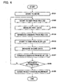
- the control section 4 first causes the scale 2 to relatively move in the direction indicated by the "A" (Step S101). Subsequently, the control section 4 causes the red LED 11 to emit red light (Step S102), and the photoreceiver 3 thereby receives the reflected light. The control section 4 then measures first data (incremental data of equal pitches) on the basis of a reception light signal from the photoreceiver 3 (Step S103). Subsequently, the control section 4 causes the red LED 11 to terminate the emission of the red light (Step S104).
- control section 4 causes the blue LED 12 to emit blue light (Step S105), and the photoreceiver 3 thereby receives the reflected light.
- the control section 4 measures second data (absolute position data) on the basis of a reception light signal from the photoreceiver 3 (Step S106).
- the control section 4 causes the blue LED 12 to terminate the emission of the blue light (Step S107).
- the control section 4 determines whether or not termination of the movement is accepted or whether or not the termination is detected (Step S108).
- the control section 4 determines that the movement is terminated ("Yes" at Step S108)
- the control section 4 derives a result of the measurement from the number of variation of the first data during the movement and the variation pattern of the second data during the movement (Step S109). The operation is then terminated.
- the control section 4 determines that the movement is not terminated ("No" at Step S108)
- the control section 4 repeatedly executes the operations of Steps S102 to S107 again.
- the photoelectric encoder By configuring the photoelectric encoder in this manner, two types of light with different wavelengths are emitted from the red LED 11 and the blue LED 12 so that the first reflection portion 21a and the second reflection portion 21b in the scale 2 respectively reflect the two types of light. Therefore, the amount of information includes wavelength information on the red light and the blue light that are reflected in the scale 2. Namely, the amount of information is increased, whereby a photoelectric encoder with high precision can be provided.
- FIGS. 5 to 7 a configuration of a photoelectric encoder according to a second embodiment of the present invention will be described with reference to FIGS. 5 to 7.
- elements identical with those of the first embodiment are assigned to the same reference numerals of the first embodiment, and descriptions thereof are omitted.
- the photoelectric encoder of the second embodiment includes a scale 2 and a control section 4 that are the same as those of the first embodiment.
- a light source 1' and a photoreceiver 3' of the photoelectric encoder are different from those of the first embodiment.
- the light source 1' of the second embodiment is differentiated from that of the first embodiment so as to include a white LED 14 in place of the read LED 11 and the blue LED 12.
- the photoreceiver 3' of the second embodiment includes a light filter unit 32 on the surface opposite to a surface to which the reflected light is emitted.
- the light filter unit 32 allows predetermined light to pass therethrough.
- the light filter unit 32 is configured from a red light filter 32a and a blue light filter 32b.
- the red light filter 32a allows only red light to pass therethrough.
- the blue light filter allows only blue light to pass therethrough.
- the photoreceiver 3' includes a red light reception area 3'a for receiving only the red light passed through the red light filter 32a and a blue light reception area 3'b for receiving only the blue light passed through the blue light filter 32b.
- the control section 4 first causes the scale 2 to relatively move in the direction "A" (Step S201). Subsequently, the control section 4 causes the white LED 14 to emit the light (Step S202). Red light of the reflected light passes through the red light filter 32a, and is received on the red light reception area 3'a of the photoreceiver 3'. The control section 4 measures first data (Step S203). Likewise, blue light of the reflected light passes through the blue light filter 32b, and is received on the blue light reception area 3'b of the photoreceiver 3'. The control section 4 measures second data (Step S204).
- the control section 4 determines whether or not termination of the movement is accepted or whether or not the termination is detected (Step S205).
- the control section 4 determines that the movement is terminated ("Yes" at Step S205)
- the control section 4 causes the white LED 14 to terminate the emission (Step S206).
- the control section 4 then derives a result of the measurement from the variation number and the variation pattern against the movement in the measured data (Step S207), and the operation is terminated.
- the control section 4 determines that the movement is not terminated ("No" at Step S205)
- the control section 4 repeatedly executes the operations of Steps S203 and S204 again.
- FIG. 9 a photoelectric encoder according to a third embodiment of the present invention will be described with reference to FIG. 9.
- elements identical with those of the first and second embodiments are assigned to the same reference numerals of the first and second embodiments, and descriptions thereof are omitted.
- the photoelectric encoder of the third embodiment includes a light source 1, a photoreceiver 3 and a control section 4 that are the same as those of the first embodiment.
- a scale 2a of the photoelectric encoder is different from that of the first embodiment.
- FIG. 10 a photoelectric encoder according to a fourth embodiment of the present invention will be described with reference to FIG. 10.
- elements identical with those of the first and second embodiments are assigned to the same reference numerals of the first and second embodiments, and descriptions thereof are omitted.
- the photoelectric encoder of the fourth embodiment includes a light source 1, a photoreceiver 3 and a control section 4 that are the same as those of the first embodiment.
- a scale 2b of the photoelectric encoder is different from that of the first embodiment.
- the photoelectric encoder By configuring the photoelectric encoder in this manner, the same effects of the first and second embodiments can be achieved. Further, since the second reflection portions 21b are arranged only in the predetermined region of the scale 2b so as to from a specific pattern as described above, the specific pattern can be utilized in useful for reading out as an origin or the like, for example.
- FIG. 11 a photoelectric encoder according to a fifth embodiment of the present invention will be described with reference to FIG. 11.
- elements identical with those of the first and second embodiments are assigned to the same reference numerals of the first and second embodiments, and descriptions thereof are omitted.
- the photoelectric encoder of the fifth embodiment includes a light source 1, a photoreceiver 3 and a control section 4 that are the same as those of the first embodiment.
- a scale 2c of the photoelectric encoder is different from that of the first embodiment.
- the same effects of the first and second embodiments can be achieved. Further, since the second reflection portions 21b are continuously arranged only in the predetermined region of the scale 2b, the pattern can be utilized in useful for reading out as an origin or the like, for example.
- FIGS. 12 to 16 a photoelectric encoder according to a sixth embodiment of the present invention will be described with reference to FIGS. 12 to 16.
- elements identical with those of the first and second embodiments are assigned to the same reference numerals of the first and second embodiments, and descriptions thereof are omitted.
- the photoelectric encoder of the sixth embodiment includes a light source 1 and a control section 4 that are the same as those of the first embodiment.
- a scale 2d and a photoreceiver 3" of the photoelectric encoder are different from those of the first embodiment.
- each of the second reflection portions 21b' is interposed between the adjacent two first reflection portions 21a so that the second reflection portions 21b' are disposed successively.
- each of the second reflection portions 21b' is formed so as to have a width of D/4 in the pitch direction and a length of H' (H' ⁇ H) in the direction perpendicular to the pitch direction.
- a red light filter unit 32' a red light reception area 3"a and a blue light reception area 3"b are different from those of the second embodiment. Namely, in the light filter unit 32', a red light filter 32'a and a blue light filter 32'b are in series aligned in a relative movement direction. A light reception array of the blue light reception area 3"b is formed so as to be rotated at 90 degrees relative to the red light reception area 3"a.
- an "X" direction is a scanning axis direction.
- a "Y” direction extends along a surface of the blue light reception area 3"b and is perpendicular to the X direction at a center of the blue light reception area 3"b.
- an amount of light received on the blue light reception area 3"b always reaches a peak at "0" position in the Y direction as shown in FIG. 14.
- a peak of the amount of light received on the blue light reception area 3"b becomes as shown in FIG. 16. Namely, the peak of the amount of light received on the blue light reception area 3"b is shifted in the Y direction with the relative movement of the photoreceiver 3" in the X direction.
- FIGS. 17 and 18 a photoelectric encoder according to a seventh embodiment of the present invention will be described with reference to FIGS. 17 and 18.
- elements identical with those of the first and second embodiments are assigned to the same reference numerals of the first and second embodiments, and descriptions thereof are omitted.
- the photoelectric encoder of the seventh embodiment includes a light source 1, a photoreceiver 3 and a control section 4 that are the same as those of the first embodiment.
- a scale 2e of the photoelectric encoder is different from that of the first embodiment.
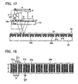
- the scale 2e differs from the scale 2 of the first embodiment in that color resists 24a are embedded in the first reflection portions 21a each having a groove shape and color resists 24b are embedded in the second reflection portions 21b each having the groove shape.
- a wavelength of the light reflected or absorbed by the color resists 24a is different from that reflected or absorbed by the color resists 24b (for example, a wavelength of the red light and that of the blue light, or the like).
- the color resists 24a of the first reflection portions 21a form an incremental scale at 10/10nm pitch intervals, for example.
- the color resists 24b of the second reflection portions 21b represent the absolute position.
- a pseudorandom code pattern may be utilized as a representation technique of the absolute position, for example.
- a maximal length sequence (M-sequence) is preferable as the pseudorandom code pattern.
- an origin pattern can be formed by the color resists 24b of the second reflection portions 21b so that the photoelectric encoder has a scale with the origin.
- a depth of each of the first reflection portions 21a may be set so as to match reflection (or absorption) efficiency of light for the color resists 24a.
- a depth of each of the second reflection portions 21b may be set so as tomatch reflection (or absorption) efficiency of light for the color resists 24b.
- the photoelectric encoder of the seventh embodiment By configuring the photoelectric encoder of the seventh embodiment in this manner, the same effects of the first and second embodiments can be achieved.
- the scale 2e has a structure that the color resists 24a, 24b are respectively embedded in the first and second reflection portions 21a, 21b, an edge of data in reproduction can be sharpened so that a scale has high definition and high precision.
- FIGS. 19 and 20 a photoelectric encoder according to an eighth embodiment of the present invention will be described with reference to FIGS. 19 and 20.
- elements identical with those of the first and second embodiments are assigned to the same reference numerals of the first and second embodiments, and descriptions thereof are omitted.
- the photoelectric encoder of the eighth embodiment includes a light source 1, a photoreceiver 3 and a control section 4 that are the same as those of the first embodiment.
- a scale 2f of the photoelectric encoder is different from that of the first embodiment.
- the scale 2f differs from the scale 2 of the first embodiment in that color resists 24a, 24b respectively functioning as the first and second reflection portions 21a, 21b are arranged on the substrate 22.
- the scale 2f has a structure that the color resists 24a, 24b respectively functioning as the first and second reflection portions 21a, 21b are formed on the substrate 22, the scale 2f can be easily manufactured compared with the case where first and second reflection portions are formed so as to have a groove shape and the color resists 24a, 24b are then respectively embedded in the first and second reflection portions.
- FIGS. 21, 22A, 22B, 23A and 23B a photoelectric encoder according to a ninth embodiment of the present invention will be described with reference to FIGS. 21, 22A, 22B, 23A and 23B.
- elements identical with those of the first and second embodiments are assigned to the same reference numerals of the first and second embodiments, and descriptions thereof are omitted.
- the photoelectric encoder of the ninth embodiment includes a light source 1, a photoreceiver 3 and a control section 4 that are the same as those of the first embodiment.
- a scale 2g of the photoelectric encoder is different from that of the first embodiment.
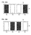
- the scale 2g differs from the scale 2 of the first embodiment in that first reflection portions 61a and second reflection portions 61b are arranged on the substrate 22 and diffraction gratings 71a, 71b are respectively formed at incident plane sides of the first reflection portions 61a and the second reflection portions 61b.
- Each of the first reflection portions 61a and the second reflection portions 61b is formed of a thin chromium film.
- the diffraction gratings 71a each having a depth "ha” are aligned at same pitch intervals in each of the first reflection portions 61a.
- the diffraction grating 71b each having a depth "hb" different from the depth "ha” are aligned at same pitch intervals in each of the second reflection portions 61b.
- each of the diffraction gratings 71a serves to diffract and reflect the light with the wavelength " ⁇ a” in a direction shown by an arrow of solid line in FIG. 22A and not to reflect the light in a direction opposite to an incidence direction of the light, shown by an arrow of dotted line in FIG. 22A.
- each of the diffraction gratings 71b serves to diffract and reflect the light with the wavelength " ⁇ b" in a direction shown by an arrow of solid line in FIG. 22A and not to reflect the light in an direction opposite to an incidence direction of the light, shown by an arrow of dotted line in FIG. 22A.
- diffraction light when the light with the wavelength " ⁇ b" reaches the surface of the first reflection portion 61a, diffraction light may be weakened due to mismatch of a condition of diffraction, thereby the light is reflected in the direction shown by an arrow of solid line in FIG. 22B.
- diffraction light when the light with the wavelength " ⁇ a" reaches the surface of the second reflection portion 61b, diffraction light may be weakened due to mismatch of a condition of diffraction, thereby the light is reflected in the direction shown by an arrow of solid line in FIG. 22B.
- the scale 2g has a structure that the first reflection portions 61a each having the diffraction grating 71a and the second reflection portions 61b each having the diffraction grating 71b are formed on the substrate 22, the scale 2g can be easily manufactured compared with the case where the first and second reflection portions are formed in a substrate so as to have a groove shape.
- a substrate 22 is first prepared.
- the substrate 22 is a plate made of a stainless steel material.
- irradiation of a laser for example, an yttrium orthovanadate (YVO4) laser
- YVO4 yttrium orthovanadate
- the substrate 22 may be a plate made of titanium other than the plate made of a stainless steel material.
- the first reflection portions 21a and the second reflection portions 21b can be formed by mainly irradiating the laser having different outputs to the substrate 22. Therefore, the scale 2 for a photoelectric encoder with high precision can be manufactured at a low cost.
- the transparent material 24 is formed on the surfaces of the substrate 22, the first reflection portions 21a and the second reflection portions 21b, corrosion resistance of the first and second reflection portions 21a, 21b can be enhanced.
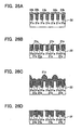
- FIG. 25A a substrate 22 is first prepared. Subsequently, resists 23a are applied to (orformedon) a surface of the substrate 22 in a first pattern as shown in FIG. 25B. Subsequently, exposure to the substrate 22 is carried out to etch the substrate 22. The resists 23a are then removed from the substrate 22 so that first grooves 21c are formed in the substrate 22 as shown in FIG. 25C. Transparent material 21d is deposited on the substrate 22 by a vapor deposition as shown in FIG. 25D. Subsequently, the substrate 22 is subjected to a chemical mechanical polishing (CMP) process so that the first reflection portions 21a are formed in the substrate 22 as shown in FIG. 25E.
- CMP chemical mechanical polishing
- resists 23b are formed on the surface of the substrate 22 in a second pattern as shown in FIG. 26A. Subsequently, exposure to the substrate 22 is carried out to etch the substrate 22. The resists 23b are then removed from the substrate 22 so that second grooves 21e are formed in the substrate 22 as shown in FIG. 26B. Transparent material 21d is deposited on the substrate 22 by the vapor deposition as shown in FIG. 26C. The substrate 22 is subjected to a CMP process so that the second reflection portions 21b are formed in the substrate 22 as shown in FIG. 26D. Thus, the scale 2 is manufactured.
- the first and second reflection portions 21a, 21b can be formed by mainly carrying out a step of forming the first and second grooves 21c, 21e by means of etching so that each of the first grooves 21c has a depth different from that of each of the second grooves 21e. Therefore, the scale 2 for a photoelectric encoder with high precision can be manufactured at a low cost.
- a third method of manufacturing a scale 2 will be described with reference to FIGS. 27A to 27M.
- a scale 2g is specifically manufactured as the scale 2 will be described.
- a substrate 22 is first prepared, and a thin chromium film 61 as light reflection portions is formed on the substrate 22 as shown in FIG. 27A.
- a resist 91 is applied to a surface of the thin chromium film 61 as shown in FIG. 27B.
- patterns 91a are formed in predetermined regions of the resist 91 for etching the thin chromium film 61 to a depth "ha" as shown in FIG. 27C.
- the predetermined regions include regions for formation of diffraction gratings 71a of first reflection portions 61a.
- the thin chromium film 61 is etched to the depth "ha" as shown in FIG. 27D.
- the resist 91 including the patterns 91a is removed from the surface of the thin chromium film 61 so that the diffraction gratings 71a are formed as shown in FIG. 27E.
- a resist 91 is then applied to the surface of the thin chromium film 61 again as shown in FIG. 27F.
- Patterns 91b are formed in predetermined regions of the resist 91 for etching the thin chromium film 61 to a depth "hb" as shown in FIG. 27G.
- the predetermined regions include regions for formation of diffraction gratings 71b of the second reflection portions 61b.
- the thin chromium film 61 is etched to a depth "hb" as shown in FIG. 27H.
- the resist 91 including the patterns 91b is removed from the surface of the thin chromium film 61 so that the diffraction gratings 71b are formed as shown in FIG. 271.
- a resist 91 is further applied to the surface of the thin chromium film 61 as shown in FIG. 27J. Patterns 91c, 91d are formed in the resist 91 for formation of the first reflection portions 61a and the second reflection portions 61b as shown in FIG. 27K.
- the thin chromium film 61 is then etched in accordance with the patterns 91c, 91d as shown in FIG. 27L.
- the resists 91 is removed as shown in FIG. 27M.
- the scale 2g with which the first reflection portions 61a each having the diffraction grating 71a and the second reflection portions 61b each having the diffraction gratings 71b are provided is manufactured.
- the first and second reflection portions 61a, 61b can be formed by mainly carrying out a step of forming the diffraction gratins 71a, 71b by means of etching so that each of the diffraction gratings 71a has a depth different from that of each of the diffraction gratings 71b. Therefore, the scale 2 for a photoelectric encoder with high precision can be manufactured at a low cost.
- the light source emits the light with different wavelengths to the scale and the scale includes a plurality of reflection portions that reflect the light with the different wavelengths respectively.
- the scale includes a plurality of reflection portions that reflect the light with the different wavelengths respectively. Therefore, light with one of the different wavelengths is reflected by one of the plurality of reflection portions. Therefore, the amount of information can be increased in accordance with the number of the different wavelengths of light reflected by the scale. The increase in the amount of information results in a photoelectric encoder with high precision. Such a photoelectric encoder can be manufactured at a low cost.
Landscapes
- Physics & Mathematics (AREA)
- General Physics & Mathematics (AREA)
- Optical Transform (AREA)
Abstract
Description
- This application is based upon and claims the benefit of priorities from
Japanese Patent Applications No. 2006-291943, filed on October 27, 2006 2007-275077, filed on October 23, 2007 - The present invention relates to a photoelectric encoder for use in precise measurement, a scale incorporated in the photoelectric encoder as an element, and a method of manufacturing the scale.
- A photoelectric encoder has been utilized in the art for precise measurement of linear displacement, angular displacement and the like. There are many types of photoelectric encoders. For example, it is proposed one type of photoelectric encoder that includes: a photoreceiver in which a plurality of photodiodes are arranged in an array manner; a scale disposed so as to be allowed to move relative to the photoreceiver and in which a reflection type of phase grating is formed; and a light source that emits light to the phase grating (See
Japanese Patent Application Publication No. 10-163549 - Since the signal light received by the photoreceiver is generated by the phase grating of the scale, the phase grating is an extremely important element of such a photoelectric encoder. Thus, it is desired means for easily manufacturing a phase grating with high precision.
- Although it is thought that the grating of the scale may be formed with high density in order to achieve the phase grating with high precision, there is a problem that the costs of manufacturing the scale with high density are increased.
- It is an object of the present invention to solve the problem described above and to provide a photoelectric encoder with high precision in which the cost of manufacturing the same is reduced to a low cost, a scale incorporated in the photoelectric encoder as an element, and a method of manufacturing the scale of the photoelectric encoder.
- In order to achieve the above object, an aspect of the present invention is directed to a photoelectric encoder. The photoelectric encoder of the present invention includes : a scale having a grating formed thereon along a measuring axis; a light source operative to emit light to the scale so as to form a light spot on the grating; and a photoreceiver operative to receive reflected light from the scale. In this case, the light source and the photoreceiver are disposed so as to be allowed to move relative to the scale at least in a direction along the measuring axis, and the light source emits the light to the scale so that the photoreceiver receives the reflected light by the scale. In addition, the light source emits light with different wavelengths, and the scale includes a plurality of reflection portions that respectively reflect the light with different wavelengths.
- Since the photoelectric encoder has the configuration described above, the light source emits the light with different wavelengths so that light with one of the different wavelengths is reflected by one of the plurality of reflection portions. Therefore, the amount of information may be increased in accordance with the number of the different wavelengths included in the light reflected by the scale. The increase of the amount of information results in a photoelectric encoder with high precision. Such a photoelectric encoder can be manufactured at a low cost.
- It is preferable that the scale includes the plurality of reflection portions respectively having different depths from a surface of the scale so that each of the plurality of reflection portions reflects the light with one of the different wavelengths in accordance with the depth thereof.
- It is preferable that the plurality of reflection portions are respectively made of a plurality of color resists, and each of the plurality of color resists reflects or absorbs the light with one of the different wavelengths. Additionally or alternatively, it is preferable that in the plurality of reflection portions, diffraction gratings are respectively formed in incidence planes thereof, and each of the diffraction gratings diffracts light with a predetermined wavelength.
- It is preferable that the light source selectively emits light with at least two wavelengths. It is preferable that the photoelectric encoder further includes: a wavelength separator operative to separate the reflected light received by the photoreceiver on the basis of each of the different wavelengths, wherein the light source emits light with a predetermined wavelength range.
- Further, according to another aspect of the present invention, the present invention is directed to a scale operative to reflect light emitted by a light source. In this case, the scale is allowed to move relative to the light source and a photoreceiver that are incorporated in a photoelectric encoder. Further, the scale includes a plurality of reflection portions each of which reflects light with one of different wavelengths.
- It is preferable that the plurality of reflection portions respectively have different depths from a surface of the scale so that each of the plurality of reflection portions reflects the light with one of the different wavelengths in accordance with the depth thereof.
- It is preferable that the plurality of reflection portions are respectively made of a plurality of color resists, and each of the plurality of color resists reflects or absorbs the light with one of the different wavelengths. Additionally or alternatively, it is preferable that in the plurality of reflection portions, diffraction gratings are respectively formed in incidence planes thereof, and each of the diffraction gratings diffracts light with a predetermined wavelength.
- Moreover, according to still another aspect of the present invention, the present invention is directed to a method of manufacturing a scale for configuration of a photoelectric encoder. The method of the present invention includes: preparing a substrate; and forming a plurality of reflection portions in a surface of the substrate at predetermined pitch intervals, the plurality of reflection portions respectively reflecting light with different wavelengths. In this case, in the forming the plurality of reflection portions includes forming the plurality of reflection portions respectively having different depths from a surface of the substrate in the surface of the substrate at the predetermined pitch intervals, and one of the plurality of reflection portions reflects light with one of different wavelengths in accordance with the depth thereof.
- It is preferable that the plurality of reflection portions are respectively made of a plurality of color resists, and each of the plurality of color resists reflects or absorbs the light with one of different wavelengths.
- It is preferable that the forming the plurality of reflection portions includes irradiating lasers respectively having different outputs to the substrate to oxidize the substrate so that each of the plurality of reflection portions has one of the different depths.
- It is preferable that the method further includes : after forming the plurality of reflection portions, forming a transparent material on surfaces of the plurality of reflection portions and the surface of the substrate.
- According to the present invention, a photoelectric encoder with high precision in which the manufacturing cost is reduced, a scale incorporated in the photoelectric encoder as an element, and a method of manufacturing the scale for the photoelectric encoder can be provided.
- The above and other objects, features and advantages of the present invention will become apparent from the following description of the preferred embodiments in conjunction with the accompanying drawings, wherein:
- FIG. 1 is a schematic diagram that shows a configuration of a photoelectric encoder according to a first embodiment of the present invention;
- FIG. 2 is a top view of a scale of the photoelectric encoder according to the first embodiment of the present invention ;
- FIG. 3 is an enlarged side cross-sectional view of the scale of the photoelectric encoder according to the first embodiment of the present invention;
- FIG. 4 is a flowchart that shows an operation of the photoelectric encoder according to the first embodiment of the present invention;
- FIG. 5 is a schematic diagram that shows a configuration of a photoelectric encoder according to a second embodiment of the present invention;
- FIG. 6 is a schematic diagram of a photoreceiver of the photoelectric encoder according to the second embodiment of the present invention;
- FIG. 7 is a cross-sectional view taken along the line A-A' shown in FIG. 6 that shows the photoreceiver of the photoelectric encoder according to the second embodiment of the present invention;
- FIG. 8 is a flowchart that shows an operation of the photoelectric encoder according to the second embodiment of the present invention;
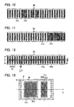
- FIG. 9 is a top view of a scale of a photoelectric encoder according to a third embodiment of the present invention;
- FIG. 10 is a top view of a scale of a photoelectric encoder according to a fourth embodiment of the present invention;
- FIG. 11 is a top view of a scale of a photoelectric encoder according to a fifth embodiment of the present invention;
- FIG. 12 a top view of a scale of a photoelectric encoder according to a sixth embodiment of the present invention;
- FIG. 13 is a schematic diagram that shows a photoreceiver of the photoelectric encoder according to the sixth embodiment of the present invention;
- FIG. 14 is a diagram that shows an amount of light received in a blue light reception area in the case where the photoreceiver and the scale of the photoelectric encoder according to the sixth embodiment of the present invention are disposed in parallel;
- FIG. 15 is a diagram that shows the case where the scale is disposed so as to be inclined relative to the photoreceiver in the photoelectric encoder according to the sixth embodiment of the present invention;
- FIG. 16 is a graph that shows a relative movement amount of the scale and the amount of light received in the blue light reception area in the case where scanning is carried out in a state where the scale is disposed so as to be inclined relative to the photoreceiver in the photoelectric encoder according to the sixth embodiment of the present invention;
- FIG. 17 is a schematic diagram that shows a configuration of a photoelectric encoder according to a seventh embodiment of the present invention;
- FIG. 18 is a top view of a scale of the photoelectric encoder according to the seventh embodiment of the present invention;
- FIG. 19 is a schematic diagram that shows a configuration of a photoelectric encoder according to an eighth embodiment of the present invention;
- FIG. 20 is a top view of a scale of the photoelectric encoder according to the eighth embodiment of the present invention;
- FIG. 21 is a side cross-sectional view that shows a part of a scale of a photoelectric encoder according to a ninth embodiment of the present invention;
- FIG. 22A is a side cross-sectional view that shows a part of the scale of the photoelectric encoder according to the ninth embodiment of the present invention;
- FIG. 22B is a side cross-sectional view that shows a part of the scale of the photoelectric encoder according to the ninth embodiment of the present invention;
- FIG. 23A is a top view that shows a part of the scale of the photoelectric encoder according to the ninth embodiment of the present invention;
- FIG. 23B is a top view that shows a part of the scale of the photoelectric encoder according to the ninth embodiment of the present invention;
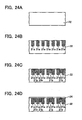
- FIG. 24A is a diagram that shows a first method of manufacturing a scale of a photoelectric encoder of the present invention;
- FIG. 24B is a diagram that shows the first method of manufacturing the scale of the photoelectric encoder of the present invention;
- FIG. 24C is a diagram that shows the first method of manufacturing the scale of the photoelectric encoder of the present invention;
- FIG. 24D is a diagram that shows the first method of manufacturing the scale of the photoelectric encoder of the present invention;
- FIG. 25A is a diagram that shows a second method of manufacturing a scale of a photoelectric encoder of the present invention;
- FIG. 25B is a diagram that shows the second method of manufacturing the scale of the photoelectric encoder of the present invention;
- FIG. 25C is a diagram that shows the second method of manufacturing the scale of the photoelectric encoder of the present invention;
- FIG. 25D is a diagram that shows the second method of manufacturing the scale of the photoelectric encoder of the present invention;
- FIG. 25E is a diagram that shows the second method of manufacturing the scale of the photoelectric encoder of the present invention;
- FIG. 26A is a diagram that shows the second method of manufacturing the scale of the photoelectric encoder of the present invention;
- FIG. 26B is a diagram that shows the second method of manufacturing the scale of the photoelectric encoder of the present invention;
- FIG. 26C is a diagram that shows the second method of manufacturing the scale of the photoelectric encoder of the present invention;
- FIG. 26D is a diagram that shows the second method of manufacturing the scale of the photoelectric encoder of the present invention;
- FIG. 27A is a diagram that shows a third method of manufacturing a scale of a photoelectric encoder of the present invention;
- FIG. 27B is a diagram that shows the third method of manufacturing the scale of the photoelectric encoder of the present invention;
- FIG. 27C is a diagram that shows the third method of manufacturing the scale of the photoelectric encoder of the present invention;
- FIG. 27D is a diagram that shows the third method of manufacturing the scale of the photoelectric encoder of the present invention;
- FIG. 27E is a diagram that shows the third method of manufacturing the scale of the photoelectric encoder of the present invention;
- FIG. 27F is a diagram that shows the third method of manufacturing the scale of the photoelectric encoder of the present invention;
- FIG. 27G is a diagram that shows the third method of manufacturing the scale of the photoelectric encoder of the present invention;
- FIG. 27H is a diagram that shows the third method of manufacturing the scale of the photoelectric encoder of the present invention;
- FIG. 27I is a diagram that shows the third method of manufacturing the scale of the photoelectric encoder of the present invention;
- FIG. 27J is a diagram that shows the third method of manufacturing the scale of the photoelectric encoder of the present invention;
- FIG. 27K is a diagram that shows the third method of manufacturing the scale of the photoelectric encoder of the present invention;
- FIG. 27L is a diagram that shows the third method of manufacturing the scale of the photoelectric encoder of the present invention; and
- FIG. 27M is a diagram that shows the third method of manufacturing the scale of the photoelectric encoder of the present invention.
- A photoelectric encoder according to preferred embodiments of the present invention will now be described with reference to the accompanying drawings.
- A configuration of a photoelectric encoder according to a first embodiment of the present invention will be described. FIG. 1 is a schematic diagramthat shows the photoelectric encoder according to the first embodiment of the present invention. As shown in FIG. 1, the photoelectric encoder of the first embodiment is configured from: a
light source 1; ascale 2 provided with a phase grating 21 for reflecting light generated by thelight source 1; aphotoreceiver 3 subjected to the light reflected by the phase grating 21; and a control section 4 for controlling drive of thephotoreceiver 3 and for deriving a measurement value from the light received by thephotoreceiver 3. The control section 4 also controls On/Off of thelight source 1. - The
light source 1 includes a red light-emitting diode (LED) 11 and ablue LED 12. For example, the red LED 11 emits light with a center wavelength of 650nm, while theblue LED 12 emits light with a center wavelength of 388nm. Thelight source 1 includes anindex scale 13a at a position where the red LED 11 and theblue LED 12 emit light thereto. Theindex scale 13a is provided on a longtransparent substrate 13. Anoptical grid 131 is formed on a surface thetransparent substrate 13, which is opposite to a surface that faces the red LED 11 and theblue LED 12. Theoptical grid 131 is configured from a plurality oflight shield portions 131a that are arranged in a linear manner at predetermined pitch intervals (as one example of an array manner). - The
scale 2 is disposed so as to be spaced with a predetermined gap from the surface of thetransparent substrate 13 that is opposite to the surface on which theoptical grid 131 of theindex scale 13a is formed. Thescale 2 is formed so as to have a length in a longitudinal direction longer than that of theindex scale 13a. A portion of thescale 2 is shown in FIG. 1. FIG. 2 shows a top view of thescale 2. FIG. 3 shows an enlarged side cross-sectional view of a part of the scale. The structure of thescale 2 will be described in detail with reference to FIGS. 1 to 3. - The
scale 2 is configured from along substrate 22 made of a stainless steel material. One surface of thesubstrate 22 is opposed to theoptical grid 131 of theindex scale 13a through thetransparent substrate 13. The phase grating 21 is formed in the surface of thesubstrate 22. The light from thelight source 1 is emitted to the phase grating 21. The phase grating 21 includesfirst reflection potions 21a each having a first depth andsecond reflection portions 21b each having a second depth shallower than the first depth. For example, each of thefirst reflection portions 21a has a depth L, while each of thesecond reflection portions 21b has a depth M. Each of thefirst reflection portions 21a is formed so as to have a width D/2 in a pitch direction and a length H in a direction perpendicular to the pitch direction. Thefirst reflection portions 21a are disposed at predetermined pitch intervals D so as to form an incremental pattern. On the other hand, thesecond reflection portions 21b are disposed so as to define absolute positional data, such as ..."1", "1", "0", "1", "0", "1", "1" "0" "1" "0" "1" "1" "0"... in the case where it is defined that "1" indicates a state where thesecond reflection portion 21b is interposed between adjacent twofirst reflection portions 21a and "0" indicates a state where thesecond reflection portion 21b is not interposed between adjacent twofirst reflection portions 21a. Each of thesecond reflection portions 21b is formed so as to have a width D/4 in the pitch direction and a length H in the direction perpendicular to the pitch direction. - Next, referring again to FIG. 1, the
photoreceiver 3 will be described. Thephotoreceiver 3 is arranged on the surface of thetransparent substrate 13 on which theoptical grid 131 of theindex scale 13a is arranged throughbumps 31 made of Au or the like. Thephotoreceiver 3 is disposed so that a receiving surface thereof faces the phase grating. 21. A charge-coupled device (CCD) or a complementary metal-oxide semiconductor (CMOS) may be utilized as thephotoreceiver 3, for example. - The
photoreceiver 3, thetransparent substrate 13 including theindex scale 13a, the red LED 11 and theblue LED 12 are accommodated within an enclosure (not shown). The enclosure is allowed to move relative to thescale 2 in a longitudinal direction of the scale 2 ("A" direction shown in FIG. 1). In other words, thescale 2 is allowed to move relative to the enclosure mentioned above in the "A" direction shown in FIG. 1. In this regard, although the photoelectric encoder is of the linear type (one-dimensional type), the present embodiment can be applied to a two-dimensional type of photoelectric encoder. - Next, a difference of optical characteristics between the
first reflection portion 21a and thesecond reflection portion 21b will be described with reference to FIG. 3. As shown in FIG. 3, the light is emitted from the red LED 11 and theblue LED 12 at an angle φ with respect to a perpendicular line to the surface of thesubstrate 22. The light emitted to thesubstrate 22 is reflected on the surface of thesubstrate 22 or a bottom of each of thefirst reflection portions 21a and each of thesecond reflection portions 21b. Here, it is assumed that an angle of incidence of the light at the bottom of each of thefirst reflection portions 21a or thesecond reflection portions 21b is indicated by "θ", and an index of refraction of each of thefirst reflection portions 21a and thesecond reflection portions 21b is indicatedby"n" (where n = sinφ/sinθ). There occurs a difference between the light reflected on the surface of thefirst reflection portion 21a and the light reflected by the bottom of the samefirst reflection portion 21a by an optical path length "a" as shown in FIG. 3. Likewise, there occurs a difference between the light reflected by the surface of thesecond reflection portion 21b and the light reflected by the bottom of the samesecond reflection portion 21b by an optical path length "a'" as shown in FIG. 3. Thus, the relationships between the respective depths of thefirst reflection portions 21a and thesecond reflection portions 21b and a wavelength of the light reflected according to the depth meet the following expressions (1) and (2).
(where "m" indicates a positive integer.)
("k" indicates a positive integer.) - The
first reflection portion 21a meets the relationship of the expression (1). Thefirst reflection portion 21a has the depth L for strengthening and reflecting red light (a wavelength thereof is 650nm). Thesecond reflection portion 21b meets the relationship of the expression (2). Thesecond reflection portion 21b has the depth M for strengthening and reflecting blue light (a wavelength thereof is 388nm). Further, thefirst reflection portion 21a and thesecond reflection portion 21b have the refractive index "n" that meets requirements of the expressions (1) and (2). - The
first reflection portions 21a formed as described above are utilized to measure incremental (INC) data by which an amount of the relative movement of thescale 2 can be calculated on the basis of the number of variation in the amount of reflection light by thefirst reflection portions 21a at the predetermined pitch intervals. Thesecond reflection portions 21b are utilized to measure absolute position (ABS) data by which an amount of relative movement of thescale 2 can be calculated on the basis of variation in a specific pattern of the amount of reflection light by thesecond reflection portions 21b. - Next, a measurement operation of the photoelectric encoder according to the first embodiment will be described with reference to FIG. 4. The control section 4 first causes the
scale 2 to relatively move in the direction indicated by the "A" (Step S101). Subsequently, the control section 4 causes the red LED 11 to emit red light (Step S102), and thephotoreceiver 3 thereby receives the reflected light. The control section 4 then measures first data (incremental data of equal pitches) on the basis of a reception light signal from the photoreceiver 3 (Step S103). Subsequently, the control section 4 causes the red LED 11 to terminate the emission of the red light (Step S104). - Subsequently, the control section 4 causes the
blue LED 12 to emit blue light (Step S105), and thephotoreceiver 3 thereby receives the reflected light. The control section 4 then measures second data (absolute position data) on the basis of a reception light signal from the photoreceiver 3 (Step S106). Subsequently, the control section 4 causes theblue LED 12 to terminate the emission of the blue light (Step S107). - The control section 4 then determines whether or not termination of the movement is accepted or whether or not the termination is detected (Step S108). Here, in the case where the control section 4 determines that the movement is terminated ("Yes" at Step S108), the control section 4 derives a result of the measurement from the number of variation of the first data during the movement and the variation pattern of the second data during the movement (Step S109). The operation is then terminated. On the other hand, in the case where the control section 4 determines that the movement is not terminated ("No" at Step S108), the control section 4 repeatedly executes the operations of Steps S102 to S107 again.
- By configuring the photoelectric encoder in this manner, two types of light with different wavelengths are emitted from the red LED 11 and the
blue LED 12 so that thefirst reflection portion 21a and thesecond reflection portion 21b in thescale 2 respectively reflect the two types of light. Therefore, the amount of information includes wavelength information on the red light and the blue light that are reflected in thescale 2. Namely, the amount of information is increased, whereby a photoelectric encoder with high precision can be provided. - Next, a configuration of a photoelectric encoder according to a second embodiment of the present invention will be described with reference to FIGS. 5 to 7. In this regard, elements identical with those of the first embodiment are assigned to the same reference numerals of the first embodiment, and descriptions thereof are omitted.
- As shown in FIG. 5, the photoelectric encoder of the second embodiment includes a
scale 2 and a control section 4 that are the same as those of the first embodiment. A light source 1' and a photoreceiver 3' of the photoelectric encoder are different from those of the first embodiment. - The light source 1' of the second embodiment is differentiated from that of the first embodiment so as to include a
white LED 14 in place of the read LED 11 and theblue LED 12. - As shown in FIGS. 5 to 7, the photoreceiver 3' of the second embodiment includes a
light filter unit 32 on the surface opposite to a surface to which the reflected light is emitted. Thelight filter unit 32 allows predetermined light to pass therethrough. - The
light filter unit 32 is configured from ared light filter 32a and a bluelight filter 32b. Thered light filter 32a allows only red light to pass therethrough. The blue light filter allows only blue light to pass therethrough. Further, the photoreceiver 3' includes a red light reception area 3'a for receiving only the red light passed through thered light filter 32a and a blue light reception area 3'b for receiving only the blue light passed through the bluelight filter 32b. - Next, a measurement operation of the photoelectric encoder of the second embodiment will be described with reference to FIG. 8. The control section 4 first causes the
scale 2 to relatively move in the direction "A" (Step S201). Subsequently, the control section 4 causes thewhite LED 14 to emit the light (Step S202). Red light of the reflected light passes through thered light filter 32a, and is received on the red light reception area 3'a of the photoreceiver 3'. The control section 4 measures first data (Step S203). Likewise, blue light of the reflected light passes through the bluelight filter 32b, and is received on the blue light reception area 3'b of the photoreceiver 3'. The control section 4 measures second data (Step S204). - The control section 4 determines whether or not termination of the movement is accepted or whether or not the termination is detected (Step S205). Here, in the case where the control section 4 determines that the movement is terminated ("Yes" at Step S205), the control section 4 causes the
white LED 14 to terminate the emission (Step S206). The control section 4 then derives a result of the measurement from the variation number and the variation pattern against the movement in the measured data (Step S207), and the operation is terminated. On the other hand, in the case where the control section 4 determines that the movement is not terminated ("No" at Step S205), the control section 4 repeatedly executes the operations of Steps S203 and S204 again. - By configuring the photoelectric encoder in this manner, the same effects of the first embodiment can be achieved.
- Next, a photoelectric encoder according to a third embodiment of the present invention will be described with reference to FIG. 9. In this regard, elements identical with those of the first and second embodiments are assigned to the same reference numerals of the first and second embodiments, and descriptions thereof are omitted.
- The photoelectric encoder of the third embodiment includes a
light source 1, aphotoreceiver 3 and a control section 4 that are the same as those of the first embodiment. Ascale 2a of the photoelectric encoder is different from that of the first embodiment. - In the
scale 2a, arrangement of thesecond reflection portions 21b relative to thefirst reflection portions 21a is different from that of thescale 2 of the first embodiment. It is assumed that thesecond reflection portions 21b are formed in a regular order of ..."1", "1", "1", "1", "0", "0", "1", "1", "1", "1", "0", "0"... in the case where it is defined that "1" indicates a state where thesecond reflection portion 21b is interposed between adjacent twofirst reflection portions 21a, and "0" indicates a state where thesecond reflection portion 21b is not interposed between adjacent twofirst reflection portions 21a. - By configuring the photoelectric encoder in this manner, the same effects of the first embodiment can be achieved.
- Next, a photoelectric encoder according to a fourth embodiment of the present invention will be described with reference to FIG. 10. In this regard, elements identical with those of the first and second embodiments are assigned to the same reference numerals of the first and second embodiments, and descriptions thereof are omitted.
- The photoelectric encoder of the fourth embodiment includes a
light source 1, aphotoreceiver 3 and a control section 4 that are the same as those of the first embodiment. Ascale 2b of the photoelectric encoder is different from that of the first embodiment. - In the
scale 2b, arrangement of thesecond reflection portions 21b relative to thefirst reflection portions 21a is different from that of thescale 2 of the first embodiment. It is assumed that thesecond reflection portions 21b are arranged in a predetermined region in an order of "0"..."0", "1", "1", "0", "0", "1", "0", "1", "0"..."0" in the case where it is defined that "1" indicates a state where thesecond reflection portion 21b is interposed between adjacent twofirst reflection portions 21a, arid "0" indicates a state where thesecond reflection portion 21b is not interposed between adjacent twofirst reflection portions 21a. - By configuring the photoelectric encoder in this manner, the same effects of the first and second embodiments can be achieved. Further, since the
second reflection portions 21b are arranged only in the predetermined region of thescale 2b so as to from a specific pattern as described above, the specific pattern can be utilized in useful for reading out as an origin or the like, for example. - Next, a photoelectric encoder according to a fifth embodiment of the present invention will be described with reference to FIG. 11. In this regard, elements identical with those of the first and second embodiments are assigned to the same reference numerals of the first and second embodiments, and descriptions thereof are omitted.
- The photoelectric encoder of the fifth embodiment includes a
light source 1, aphotoreceiver 3 and a control section 4 that are the same as those of the first embodiment. A scale 2c of the photoelectric encoder is different from that of the first embodiment. - In the scale 2c, arrangement of the
second reflection portions 21b relative to thefirst reflection portions 21a is different from that of thescale 2 of the first embodiment. It is assumed that thesecond reflection portions 21b are continuously arranged only in a predetermined region in an order of "0"..."0", "1", "1", "1", "1", "1", "1", "1", "0"..."0" in the case where it is defined that "1" indicates a state where thesecond reflection portion 21b is interposed between adjacent twofirst reflection portions 21a, and "0" indicates a state where thesecond reflection portion 21b is not interposed between adjacent twofirst reflection portions 21a. - By configuring the photoelectric encoder in this manner, the same effects of the first and second embodiments can be achieved. Further, since the
second reflection portions 21b are continuously arranged only in the predetermined region of thescale 2b, the pattern can be utilized in useful for reading out as an origin or the like, for example. - Next, a photoelectric encoder according to a sixth embodiment of the present invention will be described with reference to FIGS. 12 to 16. In this regard, elements identical with those of the first and second embodiments are assigned to the same reference numerals of the first and second embodiments, and descriptions thereof are omitted.
- The photoelectric encoder of the sixth embodiment includes a
light source 1 and a control section 4 that are the same as those of the first embodiment. Ascale 2d and aphotoreceiver 3" of the photoelectric encoder are different from those of the first embodiment. - In the
scale 2d, as shown in FIG. 12, arrangement of thesecond reflection portions 21b' relative to thefirst reflection portions 21a and the shape of eachsecond reflection portion 21b' are different fromthose of thescale 2 of the first embodiment. Thefirst reflection portions 21a and thesecond reflections portions 21b' are arranged alternately. Namely, each of thesecond reflection portions 21b' is interposed between the adjacent twofirst reflection portions 21a so that thesecond reflection portions 21b' are disposed successively. Further, each of thesecond reflection portions 21b' is formed so as to have a width of D/4 in the pitch direction and a length of H' (H' < H) in the direction perpendicular to the pitch direction. - In the
photoreceiver 3", as shown in FIG. 13, configurations of a light filter unit 32' , a redlight reception area 3"a and a bluelight reception area 3"b are different from those of the second embodiment. Namely, in the light filter unit 32', a red light filter 32'a and a blue light filter 32'b are in series aligned in a relative movement direction. A light reception array of the bluelight reception area 3"b is formed so as to be rotated at 90 degrees relative to the redlight reception area 3"a. Here, an "X" direction is a scanning axis direction. A "Y" direction extends along a surface of the bluelight reception area 3"b and is perpendicular to the X direction at a center of the bluelight reception area 3"b. - For example, in the case where the
photoreceiver 3" and thescale 2d are disposed in parallel with each other, an amount of light received on the bluelight reception area 3"b always reaches a peak at "0" position in the Y direction as shown in FIG. 14. - Further, for example, in the case where scanning is carried out in a state where the
scale 2d is inclined relative to thephotoreceiver 3" as shown in FIG. 15, a peak of the amount of light received on the bluelight reception area 3"b becomes as shown in FIG. 16. Namely, the peak of the amount of light received on the bluelight reception area 3"b is shifted in the Y direction with the relative movement of thephotoreceiver 3" in the X direction. - Therefore, according to the configuration of the photoelectric encoder of the sixth embodiment, inclination between the
photoreceiver 3" and the scale 3d can be detected. In addition, by configuring the photoelectric encoder of the sixth embodiment in this manner, the same effects of the first and second embodiments can also be achieved. - Next, a photoelectric encoder according to a seventh embodiment of the present invention will be described with reference to FIGS. 17 and 18. In this regard, elements identical with those of the first and second embodiments are assigned to the same reference numerals of the first and second embodiments, and descriptions thereof are omitted.
- The photoelectric encoder of the seventh embodiment includes a
light source 1, aphotoreceiver 3 and a control section 4 that are the same as those of the first embodiment. Ascale 2e of the photoelectric encoder is different from that of the first embodiment. - As shown in FIGS. 17 and 18, the
scale 2e differs from thescale 2 of the first embodiment in that color resists 24a are embedded in thefirst reflection portions 21a each having a groove shape and color resists 24b are embedded in thesecond reflection portions 21b each having the groove shape. A wavelength of the light reflected or absorbed by the color resists 24a is different from that reflected or absorbed by the color resists 24b (for example, a wavelength of the red light and that of the blue light, or the like). - Here, the color resists 24a of the
first reflection portions 21a form an incremental scale at 10/10nm pitch intervals, for example. The color resists 24b of thesecond reflection portions 21b represent the absolute position. Further, a pseudorandom code pattern may be utilized as a representation technique of the absolute position, for example. A maximal length sequence (M-sequence) is preferable as the pseudorandom code pattern. - Moreover, according to the
scale 2e of the seventh embodiment, an origin pattern can be formed by the color resists 24b of thesecond reflection portions 21b so that the photoelectric encoder has a scale with the origin. In this regard, a depth of each of thefirst reflection portions 21a may be set so as to match reflection (or absorption) efficiency of light for the color resists 24a. Likewise, a depth of each of thesecond reflection portions 21b may be set so as tomatch reflection (or absorption) efficiency of light for the color resists 24b. - By configuring the photoelectric encoder of the seventh embodiment in this manner, the same effects of the first and second embodiments can be achieved. In addition, since the
scale 2e has a structure that the color resists 24a, 24b are respectively embedded in the first andsecond reflection portions - Next, a photoelectric encoder according to an eighth embodiment of the present invention will be described with reference to FIGS. 19 and 20. In this regard, elements identical with those of the first and second embodiments are assigned to the same reference numerals of the first and second embodiments, and descriptions thereof are omitted.
- The photoelectric encoder of the eighth embodiment includes a
light source 1, aphotoreceiver 3 and a control section 4 that are the same as those of the first embodiment. Ascale 2f of the photoelectric encoder is different from that of the first embodiment. - As shown in FIGS. 19 and 20, the
scale 2f differs from thescale 2 of the first embodiment in that color resists 24a, 24b respectively functioning as the first andsecond reflection portions substrate 22. - By configuring the photoelectric encoder of the eighth embodiment in this manner, the same effects of the first and second embodiments can be achieved. Further, since the
scale 2f has a structure that the color resists 24a, 24b respectively functioning as the first andsecond reflection portions substrate 22, thescale 2f can be easily manufactured compared with the case where first and second reflection portions are formed so as to have a groove shape and the color resists 24a, 24b are then respectively embedded in the first and second reflection portions. - Next, a photoelectric encoder according to a ninth embodiment of the present invention will be described with reference to FIGS. 21, 22A, 22B, 23A and 23B. In this regard, elements identical with those of the first and second embodiments are assigned to the same reference numerals of the first and second embodiments, and descriptions thereof are omitted.
- The photoelectric encoder of the ninth embodiment includes a
light source 1, aphotoreceiver 3 and a control section 4 that are the same as those of the first embodiment. Ascale 2g of the photoelectric encoder is different from that of the first embodiment. - As shown in FIG. 21, the
scale 2g differs from thescale 2 of the first embodiment in thatfirst reflection portions 61a andsecond reflection portions 61b are arranged on thesubstrate 22 anddiffraction gratings first reflection portions 61a and thesecond reflection portions 61b. Each of thefirst reflection portions 61a and thesecond reflection portions 61b is formed of a thin chromium film. Thediffraction gratings 71a each having a depth "ha" are aligned at same pitch intervals in each of thefirst reflection portions 61a. The diffraction grating 71b each having a depth "hb" different from the depth "ha" are aligned at same pitch intervals in each of thesecond reflection portions 61b. - As shown in FIG. 22A, when light with a wavelength "λa" (in this case, "λa" = 4 × "ha"), for example, reaches a surface of the
first reflection portion 61a, each of thediffraction gratings 71a serves to diffract and reflect the light with the wavelength "λa" in a direction shown by an arrow of solid line in FIG. 22A and not to reflect the light in a direction opposite to an incidence direction of the light, shown by an arrow of dotted line in FIG. 22A. Likewise, when light with a wavelength "λb" (λb" = 4 × "hb"), for example, reaches a surface of thesecond reflection portion 61b, each of thediffraction gratings 71b serves to diffract and reflect the light with the wavelength "λb" in a direction shown by an arrow of solid line in FIG. 22A and not to reflect the light in an direction opposite to an incidence direction of the light, shown by an arrow of dotted line in FIG. 22A. - On the other hand, as shown in FIG. 22B, when the light with the wavelength "λb" reaches the surface of the
first reflection portion 61a, diffraction light may be weakened due to mismatch of a condition of diffraction, thereby the light is reflected in the direction shown by an arrow of solid line in FIG. 22B. Likewise, when the light with the wavelength "λa" reaches the surface of thesecond reflection portion 61b, diffraction light may be weakened due to mismatch of a condition of diffraction, thereby the light is reflected in the direction shown by an arrow of solid line in FIG. 22B. - Namely, when the
scale 2g having the structure described above is measured using the light with the wavelength "λa", thefirst reflection portions 61a cannot be detected and thesecond reflection portions 61b can be detected as shown in FIG. 23A. On the other hand, when thescale 2g is measured using the light with the wavelength "λb", thefirst reflection portions 61a can be detected and thesecond reflection portions 61b cannot be detected as shown in FIG. 23B. - By configuring the photoelectric encoder of the ninth embodiment in this manner, the same effects of the first and second embodiments can be achieved. In addition, since the
scale 2g has a structure that thefirst reflection portions 61a each having thediffraction grating 71a and thesecond reflection portions 61b each having thediffraction grating 71b are formed on thesubstrate 22, thescale 2g can be easily manufactured compared with the case where the first and second reflection portions are formed in a substrate so as to have a groove shape. - Next, a first method of manufacturing a
scale 2 will now be described with reference to FIGS. 24A to 24D. As shown in FIG. 24A, asubstrate 22 is first prepared. As described above, thesubstrate 22 is a plate made of a stainless steel material. Subsequently, irradiation of a laser (for example, an yttrium orthovanadate (YVO4) laser) with a first output is carried out at predetermined pitch intervals so that a surface of thesubstrate 22 is oxidized, wherebyfirst reflection portions 21a are formed with an oxidized film as shown in FIG. 24B. Subsequently, irradiation of a laser with a second output smaller than the first output is carried out so that the surface of thesubstrate 22 is oxidized, whereby thesecond reflection portions 21b are formed with an oxidized film as shown in FIG. 24C. A transparent material is then formed on the surface of thesubstrate 22 and surfaces of the first andsecond reflection portions scale 2 as shown in FIG. 24D. In this regard, thesubstrate 22 may be a plate made of titanium other than the plate made of a stainless steel material. - According to the first method of manufacturing the
scale 2, thefirst reflection portions 21a and thesecond reflection portions 21b can be formed by mainly irradiating the laser having different outputs to thesubstrate 22. Therefore, thescale 2 for a photoelectric encoder with high precision can be manufactured at a low cost. In addition, since thetransparent material 24 is formed on the surfaces of thesubstrate 22, thefirst reflection portions 21a and thesecond reflection portions 21b, corrosion resistance of the first andsecond reflection portions - A second method of manufacturing a
scale 2 will be described with reference to FIGS. 25A to 25E and 26A to 26B. As shown in FIG. 25A, asubstrate 22 is first prepared. Subsequently, resists 23a are applied to (orformedon) a surface of thesubstrate 22 in a first pattern as shown in FIG. 25B. Subsequently, exposure to thesubstrate 22 is carried out to etch thesubstrate 22. The resists 23a are then removed from thesubstrate 22 so thatfirst grooves 21c are formed in thesubstrate 22 as shown in FIG. 25C.Transparent material 21d is deposited on thesubstrate 22 by a vapor deposition as shown in FIG. 25D. Subsequently, thesubstrate 22 is subjected to a chemical mechanical polishing (CMP) process so that thefirst reflection portions 21a are formed in thesubstrate 22 as shown in FIG. 25E. - Subsequently, resists 23b are formed on the surface of the
substrate 22 in a second pattern as shown in FIG. 26A. Subsequently, exposure to thesubstrate 22 is carried out to etch thesubstrate 22. The resists 23b are then removed from thesubstrate 22 so thatsecond grooves 21e are formed in thesubstrate 22 as shown in FIG. 26B.Transparent material 21d is deposited on thesubstrate 22 by the vapor deposition as shown in FIG. 26C. Thesubstrate 22 is subjected to a CMP process so that thesecond reflection portions 21b are formed in thesubstrate 22 as shown in FIG. 26D. Thus, thescale 2 is manufactured. - According to the second method of manufacturing the
scale 2, the first andsecond reflection portions second grooves first grooves 21c has a depth different from that of each of thesecond grooves 21e. Therefore, thescale 2 for a photoelectric encoder with high precision can be manufactured at a low cost. - A third method of manufacturing a
scale 2 will be described with reference to FIGS. 27A to 27M. Here, the case where ascale 2g is specifically manufactured as thescale 2 will be described. Asubstrate 22 is first prepared, and athin chromium film 61 as light reflection portions is formed on thesubstrate 22 as shown in FIG. 27A. Subsequently, a resist 91 is applied to a surface of thethin chromium film 61 as shown in FIG. 27B. Subsequently,patterns 91a are formed in predetermined regions of the resist 91 for etching thethin chromium film 61 to a depth "ha" as shown in FIG. 27C. The predetermined regions include regions for formation ofdiffraction gratings 71a offirst reflection portions 61a. In accordance with thepatterns 91a, thethin chromium film 61 is etched to the depth "ha" as shown in FIG. 27D. - The resist 91 including the
patterns 91a is removed from the surface of thethin chromium film 61 so that thediffraction gratings 71a are formed as shown in FIG. 27E. A resist 91 is then applied to the surface of thethin chromium film 61 again as shown in FIG. 27F.Patterns 91b are formed in predetermined regions of the resist 91 for etching thethin chromium film 61 to a depth "hb" as shown in FIG. 27G. The predetermined regions include regions for formation ofdiffraction gratings 71b of thesecond reflection portions 61b. In accordance with thepatterns 91b, thethin chromium film 61 is etched to a depth "hb" as shown in FIG. 27H. - Subsequently, the resist 91 including the
patterns 91b is removed from the surface of thethin chromium film 61 so that thediffraction gratings 71b are formed as shown in FIG. 271. A resist 91 is further applied to the surface of thethin chromium film 61 as shown in FIG. 27J.Patterns first reflection portions 61a and thesecond reflection portions 61b as shown in FIG. 27K. Thethin chromium film 61 is then etched in accordance with thepatterns scale 2g with which thefirst reflection portions 61a each having thediffraction grating 71a and thesecond reflection portions 61b each having thediffraction gratings 71b are provided is manufactured. - According to the third method of manufacturing the
scale 2, the first andsecond reflection portions diffraction gratins diffraction gratings 71a has a depth different from that of each of thediffraction gratings 71b. Therefore, thescale 2 for a photoelectric encoder with high precision can be manufactured at a low cost. - As described above, according to the photoelectric encoder of the present invention, a scale incorporated in the photoelectric encoder as an element, and a method of manufacturing the scale of the photoelectric encoder of the present invention, the light source emits the light with different wavelengths to the scale and the scale includes a plurality of reflection portions that reflect the light with the different wavelengths respectively. Thus, light with one of the different wavelengths is reflected by one of the plurality of reflection portions. Therefore, the amount of information can be increased in accordance with the number of the different wavelengths of light reflected by the scale. The increase in the amount of information results in a photoelectric encoder with high precision. Such a photoelectric encoder can be manufactured at a low cost.
Claims (14)
- A photoelectric encoder comprising ;a scale having a grating formed thereon along a measuring axis;a light source operative to emit light to the scale so as to form a light spot on the grating; anda photoreceiver operative to receive reflected light from the scale,wherein the light source and the photoreceiver are disposed so as to be allowed to move relative to the scale at least in a direction along the measuring axis,
wherein the light source emits the light to the scale so that the photoreceiver receives the reflected light by the scale,
wherein the light source emits light with different wavelengths, and
wherein the scale includes a plurality of reflection portions that respectively reflect the light with different wavelengths. - The photoelectric encoder according to claim 1, wherein the scale includes the plurality of reflection portions respectively having different depths from a surface of the scale so that each of the plurality of reflection portions reflects the light with one of the different wavelengths in accordance with the depth thereof.
- The photoelectric encoder according to claim 1, wherein the plurality of reflection portions are respectively made of a plurality of color resists, and each of the plurality of color resists reflects or absorbs the light with one of the different wavelengths.
- The photoelectric encoder according to claim 1, wherein in the plurality of reflection portions, diffraction gratings are respectively formed in incidence planes thereof, and each of the diffraction gratings diffracts light with a predetermined wavelength.
- The photoelectric encoder according to claim 1, wherein the light source selectively emits light with at least two wavelengths.
- The photoelectric encoder according to claim 1, further comprising:a wavelength separator operative to separate the reflected light received by the photoreceiver on the basis of each of the different wavelengths,wherein the light source emits light with a predetermined wavelength range.
- A scale operative to reflect light emitted by a light source, the scale being allowed to move relative to the light source and a photoreceiver that are incorporated in a photoelectric encoder, wherein the scale includes a plurality of reflection portions each of which reflects light with one of different wavelengths.
- The scale according to claim 7, wherein the plurality of reflection portions respectively have different depths from a surface of the scale so that each of the plurality of reflection portions reflects the light with one of the different wavelengths in accordance with the depth thereof.
- The scale according to claim 7, wherein the plurality of reflection portions are respectively made of a plurality of color resists, and each of the plurality of color resists reflects or absorbs the light with one of the different wavelengths.
- The scale according to claim 7, wherein in the plurality of reflection portions, diffraction gratings are respectively formed in incidence planes thereof, and each of the diffraction gratings diffracts light with a predetermined wavelength.
- A method of manufacturing a scale for configuration of a photoelectric encoder, the method comprising:preparing a substrate; andforming a plurality of reflection portions in a surface of the substrate at predetermined pitch intervals, the plurality of reflection portions respectively reflecting light with different wavelengths,wherein the forming the plurality of reflection portions includes forming the plurality of reflection portions respectively having different depths from a surface of the substrate in the surface of the substrate at the predetermined pitch intervals, and one of the plurality of reflection portions reflects light with one of different wavelengths in accordance with the depth thereof.
- The method according to claim 11, wherein the plurality of reflection portions are respectively made of a plurality of color resists, and each of the pluralityof color resists reflects or absorbs the light with one of different wavelengths.
- The method according to claim 11, wherein the forming the plurality of reflection portions includes irradiating lasers respectively having different outputs to the substrate to oxidize the substrate so that each of the plurality of reflection portions has one of the different depths.
- The method according to claim 11, further comprising:after forming the plurality of reflection portions, forming a transparent material on surfaces of the plurality of reflection portions and the surface of the substrate.
Applications Claiming Priority (2)
| Application Number | Priority Date | Filing Date | Title |
|---|---|---|---|
| JP2006291943 | 2006-10-27 | ||
| JP2007275077A JP5347155B2 (en) | 2006-10-27 | 2007-10-23 | Photoelectric encoder, scale, and method of manufacturing scale |
Publications (2)
| Publication Number | Publication Date |
|---|---|
| EP1916505A1 true EP1916505A1 (en) | 2008-04-30 |
| EP1916505B1 EP1916505B1 (en) | 2016-04-27 |
Family
ID=39048743
Family Applications (1)
| Application Number | Title | Priority Date | Filing Date |
|---|---|---|---|
| EP07020944.0A Not-in-force EP1916505B1 (en) | 2006-10-27 | 2007-10-25 | Photoelectric encoder, scale and method of manufacturing scale |
Country Status (3)
| Country | Link |
|---|---|
| US (1) | US7619208B2 (en) |
| EP (1) | EP1916505B1 (en) |
| JP (1) | JP5347155B2 (en) |
Cited By (2)
| Publication number | Priority date | Publication date | Assignee | Title |
|---|---|---|---|---|
| CN110686712A (en) * | 2019-11-22 | 2020-01-14 | 中国科学院长春光学精密机械与物理研究所 | A reflective image photoelectric encoder |
| CN114364948A (en) * | 2019-09-13 | 2022-04-15 | 应用材料公司 | Measurement system and grating pattern array |
Families Citing this family (21)
| Publication number | Priority date | Publication date | Assignee | Title |
|---|---|---|---|---|
| JP5434379B2 (en) * | 2009-08-28 | 2014-03-05 | 株式会社ニコン | Scale body, position detection apparatus, stage apparatus, and exposure apparatus |
| JP5560847B2 (en) * | 2010-03-31 | 2014-07-30 | 株式会社ニコン | Encoder |
| JP5379761B2 (en) * | 2010-08-06 | 2013-12-25 | キヤノン株式会社 | Absolute encoder |
| EP2527156A1 (en) * | 2011-05-25 | 2012-11-28 | RLS Merilna Tehnika D.O.O. | Apparatus and method for writing a pattern in a substrate |
| CN102313517B (en) * | 2011-08-23 | 2013-01-09 | 广州市诺信数字测控设备有限公司 | Optical grating ruler with double light sources |
| US20130221212A1 (en) * | 2012-02-24 | 2013-08-29 | Avago Technologies Ecbu Ip (Singapore) Pte. Ltd. | Coding Members With Embedded Metal Layers For Encoders |
| DE102012221566A1 (en) * | 2012-11-26 | 2014-05-28 | Dr. Johannes Heidenhain Gmbh | Optical position measuring device |
| JP6366274B2 (en) * | 2014-01-07 | 2018-08-01 | キヤノン株式会社 | Scale, measuring apparatus, image forming apparatus, scale processing apparatus, and scale processing method |
| JP6359340B2 (en) * | 2014-05-27 | 2018-07-18 | 株式会社ミツトヨ | Scale and optical encoder |
| US9562793B2 (en) * | 2014-11-17 | 2017-02-07 | Mitutoyo Corporation | Illumination portion for an optical encoder |
| TWI592637B (en) | 2014-11-21 | 2017-07-21 | 財團法人工業技術研究院 | Optical encoder |
| WO2017045704A1 (en) * | 2015-09-15 | 2017-03-23 | Pepperl+Fuchs Gmbh | Apparatus and method for reliably determining the position of an object |
| DE102016204313A1 (en) * | 2016-03-16 | 2017-09-21 | Dr. Johannes Heidenhain Gesellschaft Mit Beschränkter Haftung | Optical distance sensor and position measuring device with such a distance sensor |
| US10303270B2 (en) * | 2016-09-12 | 2019-05-28 | Microsoft Technology Licensing, Llc | Linear encoder force transducer |
| TWI648520B (en) | 2016-10-21 | 2019-01-21 | 財團法人工業技術研究院 | Optical encoding device |
| JP7140495B2 (en) * | 2017-12-28 | 2022-09-21 | 株式会社ミツトヨ | Scale and its manufacturing method |
| TWI680648B (en) | 2018-12-26 | 2019-12-21 | 財團法人工業技術研究院 | Code disk, optical detector, optical absolute rotary encoder and method for outputting, error detecting and correcting code values |
| JP7391527B2 (en) * | 2019-04-03 | 2023-12-05 | 株式会社ミツトヨ | photoelectric encoder |
| TWI716246B (en) | 2019-12-31 | 2021-01-11 | 財團法人工業技術研究院 | Optical encoder |
| JP2023032576A (en) * | 2021-08-27 | 2023-03-09 | ローム株式会社 | Position sensing device |
| US20250109970A1 (en) * | 2023-09-28 | 2025-04-03 | Apple Inc. | Optical sensors having an absence of guard structures between adjacent photodiodes |
Citations (5)
| Publication number | Priority date | Publication date | Assignee | Title |
|---|---|---|---|---|
| US4774494A (en) | 1985-08-01 | 1988-09-27 | Lucas Industries Public Limited Company | Position encoder employing three or more colors |
| EP0498904A1 (en) | 1991-02-11 | 1992-08-19 | Dr. Johannes Heidenhain GmbH | Photo-electric position measuring device |
| WO2006109020A1 (en) | 2005-04-13 | 2006-10-19 | Renishaw Plc | Method of scale manufacture with laser and sensor and feedback means for producing scale marking with desired depth |
| JP2006291943A (en) | 2005-04-12 | 2006-10-26 | Junji Takahara | Storm countermeasure structure for wind power generator |
| JP2007275077A (en) | 2000-10-10 | 2007-10-25 | Seikagaku Kogyo Co Ltd | Monoclonal antibody against chondroitinase abc |
Family Cites Families (3)
| Publication number | Priority date | Publication date | Assignee | Title |
|---|---|---|---|---|
| US5216245A (en) * | 1991-10-04 | 1993-06-01 | General Motors Corporation | Multi-color optical shaft position sensor |
| JPH05118876A (en) * | 1991-10-28 | 1993-05-14 | Tamagawa Seiki Co Ltd | Optical fiber encoder |
| JPH10163549A (en) | 1996-12-03 | 1998-06-19 | Nikon Corp | Laser light source device and laser light source support structure |
-
2007
- 2007-10-23 JP JP2007275077A patent/JP5347155B2/en not_active Expired - Fee Related
- 2007-10-25 EP EP07020944.0A patent/EP1916505B1/en not_active Not-in-force
- 2007-10-25 US US11/976,542 patent/US7619208B2/en not_active Expired - Fee Related
Patent Citations (5)
| Publication number | Priority date | Publication date | Assignee | Title |
|---|---|---|---|---|
| US4774494A (en) | 1985-08-01 | 1988-09-27 | Lucas Industries Public Limited Company | Position encoder employing three or more colors |
| EP0498904A1 (en) | 1991-02-11 | 1992-08-19 | Dr. Johannes Heidenhain GmbH | Photo-electric position measuring device |
| JP2007275077A (en) | 2000-10-10 | 2007-10-25 | Seikagaku Kogyo Co Ltd | Monoclonal antibody against chondroitinase abc |
| JP2006291943A (en) | 2005-04-12 | 2006-10-26 | Junji Takahara | Storm countermeasure structure for wind power generator |
| WO2006109020A1 (en) | 2005-04-13 | 2006-10-19 | Renishaw Plc | Method of scale manufacture with laser and sensor and feedback means for producing scale marking with desired depth |
Cited By (3)
| Publication number | Priority date | Publication date | Assignee | Title |
|---|---|---|---|---|
| CN114364948A (en) * | 2019-09-13 | 2022-04-15 | 应用材料公司 | Measurement system and grating pattern array |
| CN114364948B (en) * | 2019-09-13 | 2024-06-11 | 应用材料公司 | Measuring system and grating pattern array |
| CN110686712A (en) * | 2019-11-22 | 2020-01-14 | 中国科学院长春光学精密机械与物理研究所 | A reflective image photoelectric encoder |
Also Published As
| Publication number | Publication date |
|---|---|
| JP5347155B2 (en) | 2013-11-20 |
| US7619208B2 (en) | 2009-11-17 |
| JP2008134235A (en) | 2008-06-12 |
| US20080099666A1 (en) | 2008-05-01 |
| EP1916505B1 (en) | 2016-04-27 |
Similar Documents
| Publication | Publication Date | Title |
|---|---|---|
| EP1916505B1 (en) | Photoelectric encoder, scale and method of manufacturing scale | |
| US6713756B2 (en) | Optical encoder and optical rotary encoder | |
| JP4208483B2 (en) | Optical encoder | |
| US7129475B2 (en) | Photoelectric encoder and method of manufacturing scales | |
| US8188421B2 (en) | Optical encoder for detecting the relative displacement between an encoder scale and an encoder head | |
| JP4427540B2 (en) | Optical encoder | |
| EP1722201B1 (en) | Optical encoder | |
| EP2889586B1 (en) | Optical encoder | |
| EP3347681B1 (en) | Encoder apparatus | |
| JP6563813B2 (en) | Optical element | |
| JP6850136B2 (en) | Optical position measuring device | |
| CN1293367C (en) | Reference point talbot encoder | |
| US10190893B2 (en) | Encoder | |
| CN107044861B (en) | Photoelectric encoder | |
| JP2021193354A (en) | Optical encoder and control device | |
| JP6761974B2 (en) | Photodetector and photodetector | |
| JP4543311B2 (en) | Optical encoder | |
| JP4578210B2 (en) | Optical displacement measuring device | |
| JP2025136513A (en) | Optical system and position detection method | |
| JP3847283B2 (en) | Optical encoder | |
| TW202546411A (en) | Optical sensor for simultaneous displacement sensing and multi/hyperspectral imaging | |
| JP2024076303A (en) | Optical Encoders | |
| JP2015055532A (en) | Reflective encoder device | |
| JP2005291794A (en) | Optical encoder | |
| JP2011112522A (en) | Oblique incidence interferometer |
Legal Events
| Date | Code | Title | Description |
|---|---|---|---|
| PUAI | Public reference made under article 153(3) epc to a published international application that has entered the european phase |
Free format text: ORIGINAL CODE: 0009012 |
|
| AK | Designated contracting states |
Kind code of ref document: A1 Designated state(s): AT BE BG CH CY CZ DE DK EE ES FI FR GB GR HU IE IS IT LI LT LU LV MC MT NL PL PT RO SE SI SK TR |
|
| AX | Request for extension of the european patent |
Extension state: AL BA HR MK RS |
|
| 17P | Request for examination filed |
Effective date: 20081030 |
|
| AKX | Designation fees paid |
Designated state(s): DE FR GB |
|
| 17Q | First examination report despatched |
Effective date: 20150302 |
|
| GRAP | Despatch of communication of intention to grant a patent |
Free format text: ORIGINAL CODE: EPIDOSNIGR1 |
|
| INTG | Intention to grant announced |
Effective date: 20151222 |
|
| GRAS | Grant fee paid |
Free format text: ORIGINAL CODE: EPIDOSNIGR3 |
|
| GRAA | (expected) grant |
Free format text: ORIGINAL CODE: 0009210 |
|
| AK | Designated contracting states |
Kind code of ref document: B1 Designated state(s): DE FR GB |
|
| REG | Reference to a national code |
Ref country code: GB Ref legal event code: FG4D |
|
| REG | Reference to a national code |
Ref country code: DE Ref legal event code: R096 Ref document number: 602007045997 Country of ref document: DE |
|
| REG | Reference to a national code |
Ref country code: FR Ref legal event code: PLFP Year of fee payment: 10 |
|
| REG | Reference to a national code |
Ref country code: DE Ref legal event code: R097 Ref document number: 602007045997 Country of ref document: DE |
|
| PGFP | Annual fee paid to national office [announced via postgrant information from national office to epo] |
Ref country code: FR Payment date: 20161020 Year of fee payment: 10 Ref country code: GB Payment date: 20161020 Year of fee payment: 10 Ref country code: DE Payment date: 20161020 Year of fee payment: 10 |
|
| PLBE | No opposition filed within time limit |
Free format text: ORIGINAL CODE: 0009261 |
|
| STAA | Information on the status of an ep patent application or granted ep patent |
Free format text: STATUS: NO OPPOSITION FILED WITHIN TIME LIMIT |
|
| 26N | No opposition filed |
Effective date: 20170130 |
|
| REG | Reference to a national code |
Ref country code: DE Ref legal event code: R119 Ref document number: 602007045997 Country of ref document: DE |
|
| GBPC | Gb: european patent ceased through non-payment of renewal fee |
Effective date: 20171025 |
|
| REG | Reference to a national code |
Ref country code: FR Ref legal event code: ST Effective date: 20180629 |
|
| PG25 | Lapsed in a contracting state [announced via postgrant information from national office to epo] |
Ref country code: GB Free format text: LAPSE BECAUSE OF NON-PAYMENT OF DUE FEES Effective date: 20171025 Ref country code: DE Free format text: LAPSE BECAUSE OF NON-PAYMENT OF DUE FEES Effective date: 20180501 |
|
| PG25 | Lapsed in a contracting state [announced via postgrant information from national office to epo] |
Ref country code: FR Free format text: LAPSE BECAUSE OF NON-PAYMENT OF DUE FEES Effective date: 20171031 |