EP1915039A2 - Method of manufacturing circuit board - Google Patents
Method of manufacturing circuit board Download PDFInfo
- Publication number
- EP1915039A2 EP1915039A2 EP07020024A EP07020024A EP1915039A2 EP 1915039 A2 EP1915039 A2 EP 1915039A2 EP 07020024 A EP07020024 A EP 07020024A EP 07020024 A EP07020024 A EP 07020024A EP 1915039 A2 EP1915039 A2 EP 1915039A2
- Authority
- EP
- European Patent Office
- Prior art keywords
- contact
- fixed
- movable contact
- fixed contact
- circuit board
- Prior art date
- Legal status (The legal status is an assumption and is not a legal conclusion. Google has not performed a legal analysis and makes no representation as to the accuracy of the status listed.)
- Granted
Links
Images





Classifications
-
- H—ELECTRICITY
- H05—ELECTRIC TECHNIQUES NOT OTHERWISE PROVIDED FOR
- H05K—PRINTED CIRCUITS; CASINGS OR CONSTRUCTIONAL DETAILS OF ELECTRIC APPARATUS; MANUFACTURE OF ASSEMBLAGES OF ELECTRICAL COMPONENTS
- H05K3/00—Apparatus or processes for manufacturing printed circuits
- H05K3/22—Secondary treatment of printed circuits
- H05K3/24—Reinforcing of the conductive pattern
- H05K3/244—Finish plating of conductors, especially of copper conductors, e.g. for pads or lands
-
- C—CHEMISTRY; METALLURGY
- C23—COATING METALLIC MATERIAL; COATING MATERIAL WITH METALLIC MATERIAL; CHEMICAL SURFACE TREATMENT; DIFFUSION TREATMENT OF METALLIC MATERIAL; COATING BY VACUUM EVAPORATION, BY SPUTTERING, BY ION IMPLANTATION OR BY CHEMICAL VAPOUR DEPOSITION, IN GENERAL; INHIBITING CORROSION OF METALLIC MATERIAL OR INCRUSTATION IN GENERAL
- C23C—COATING METALLIC MATERIAL; COATING MATERIAL WITH METALLIC MATERIAL; SURFACE TREATMENT OF METALLIC MATERIAL BY DIFFUSION INTO THE SURFACE, BY CHEMICAL CONVERSION OR SUBSTITUTION; COATING BY VACUUM EVAPORATION, BY SPUTTERING, BY ION IMPLANTATION OR BY CHEMICAL VAPOUR DEPOSITION, IN GENERAL
- C23C28/00—Coating for obtaining at least two superposed coatings either by methods not provided for in a single one of groups C23C2/00 - C23C26/00 or by combinations of methods provided for in subclasses C23C and C25C or C25D
- C23C28/02—Coating for obtaining at least two superposed coatings either by methods not provided for in a single one of groups C23C2/00 - C23C26/00 or by combinations of methods provided for in subclasses C23C and C25C or C25D only coatings only including layers of metallic material
- C23C28/023—Coating for obtaining at least two superposed coatings either by methods not provided for in a single one of groups C23C2/00 - C23C26/00 or by combinations of methods provided for in subclasses C23C and C25C or C25D only coatings only including layers of metallic material only coatings of metal elements only
-
- C—CHEMISTRY; METALLURGY
- C25—ELECTROLYTIC OR ELECTROPHORETIC PROCESSES; APPARATUS THEREFOR
- C25D—PROCESSES FOR THE ELECTROLYTIC OR ELECTROPHORETIC PRODUCTION OF COATINGS; ELECTROFORMING; APPARATUS THEREFOR
- C25D5/00—Electroplating characterised by the process; Pretreatment or after-treatment of workpieces
- C25D5/10—Electroplating with more than one layer of the same or of different metals
- C25D5/12—Electroplating with more than one layer of the same or of different metals at least one layer being of nickel or chromium
-
- C—CHEMISTRY; METALLURGY
- C25—ELECTROLYTIC OR ELECTROPHORETIC PROCESSES; APPARATUS THEREFOR
- C25D—PROCESSES FOR THE ELECTROLYTIC OR ELECTROPHORETIC PRODUCTION OF COATINGS; ELECTROFORMING; APPARATUS THEREFOR
- C25D5/00—Electroplating characterised by the process; Pretreatment or after-treatment of workpieces
- C25D5/34—Pretreatment of metallic surfaces to be electroplated
-
- H—ELECTRICITY
- H01—ELECTRIC ELEMENTS
- H01H—ELECTRIC SWITCHES; RELAYS; SELECTORS; EMERGENCY PROTECTIVE DEVICES
- H01H1/00—Contacts
- H01H1/02—Contacts characterised by the material thereof
- H01H1/021—Composite material
- H01H1/023—Composite material having a noble metal as the basic material
-
- H—ELECTRICITY
- H01—ELECTRIC ELEMENTS
- H01H—ELECTRIC SWITCHES; RELAYS; SELECTORS; EMERGENCY PROTECTIVE DEVICES
- H01H1/00—Contacts
- H01H1/12—Contacts characterised by the manner in which co-operating contacts engage
- H01H1/36—Contacts characterised by the manner in which co-operating contacts engage by sliding
- H01H1/40—Contact mounted so that its contact-making surface is flush with adjoining insulation
- H01H1/403—Contacts forming part of a printed circuit
-
- H—ELECTRICITY
- H05—ELECTRIC TECHNIQUES NOT OTHERWISE PROVIDED FOR
- H05K—PRINTED CIRCUITS; CASINGS OR CONSTRUCTIONAL DETAILS OF ELECTRIC APPARATUS; MANUFACTURE OF ASSEMBLAGES OF ELECTRICAL COMPONENTS
- H05K1/00—Printed circuits
- H05K1/02—Details
- H05K1/11—Printed elements for providing electric connections to or between printed circuits
-
- H—ELECTRICITY
- H05—ELECTRIC TECHNIQUES NOT OTHERWISE PROVIDED FOR
- H05K—PRINTED CIRCUITS; CASINGS OR CONSTRUCTIONAL DETAILS OF ELECTRIC APPARATUS; MANUFACTURE OF ASSEMBLAGES OF ELECTRICAL COMPONENTS
- H05K2203/00—Indexing scheme relating to apparatus or processes for manufacturing printed circuits covered by H05K3/00
- H05K2203/02—Details related to mechanical or acoustic processing, e.g. drilling, punching, cutting, using ultrasound
- H05K2203/025—Abrading, e.g. grinding or sand blasting
-
- H—ELECTRICITY
- H05—ELECTRIC TECHNIQUES NOT OTHERWISE PROVIDED FOR
- H05K—PRINTED CIRCUITS; CASINGS OR CONSTRUCTIONAL DETAILS OF ELECTRIC APPARATUS; MANUFACTURE OF ASSEMBLAGES OF ELECTRICAL COMPONENTS
- H05K2203/00—Indexing scheme relating to apparatus or processes for manufacturing printed circuits covered by H05K3/00
- H05K2203/03—Metal processing
- H05K2203/0392—Pretreatment of metal, e.g. before finish plating, etching
-
- H—ELECTRICITY
- H05—ELECTRIC TECHNIQUES NOT OTHERWISE PROVIDED FOR
- H05K—PRINTED CIRCUITS; CASINGS OR CONSTRUCTIONAL DETAILS OF ELECTRIC APPARATUS; MANUFACTURE OF ASSEMBLAGES OF ELECTRICAL COMPONENTS
- H05K3/00—Apparatus or processes for manufacturing printed circuits
- H05K3/22—Secondary treatment of printed circuits
- H05K3/26—Cleaning or polishing of the conductive pattern
-
- Y—GENERAL TAGGING OF NEW TECHNOLOGICAL DEVELOPMENTS; GENERAL TAGGING OF CROSS-SECTIONAL TECHNOLOGIES SPANNING OVER SEVERAL SECTIONS OF THE IPC; TECHNICAL SUBJECTS COVERED BY FORMER USPC CROSS-REFERENCE ART COLLECTIONS [XRACs] AND DIGESTS
- Y10—TECHNICAL SUBJECTS COVERED BY FORMER USPC
- Y10T—TECHNICAL SUBJECTS COVERED BY FORMER US CLASSIFICATION
- Y10T29/00—Metal working
- Y10T29/49—Method of mechanical manufacture
- Y10T29/49002—Electrical device making
- Y10T29/49117—Conductor or circuit manufacturing
- Y10T29/49124—On flat or curved insulated base, e.g., printed circuit, etc.
- Y10T29/49155—Manufacturing circuit on or in base
-
- Y—GENERAL TAGGING OF NEW TECHNOLOGICAL DEVELOPMENTS; GENERAL TAGGING OF CROSS-SECTIONAL TECHNOLOGIES SPANNING OVER SEVERAL SECTIONS OF THE IPC; TECHNICAL SUBJECTS COVERED BY FORMER USPC CROSS-REFERENCE ART COLLECTIONS [XRACs] AND DIGESTS
- Y10—TECHNICAL SUBJECTS COVERED BY FORMER USPC
- Y10T—TECHNICAL SUBJECTS COVERED BY FORMER US CLASSIFICATION
- Y10T29/00—Metal working
- Y10T29/49—Method of mechanical manufacture
- Y10T29/49002—Electrical device making
- Y10T29/49117—Conductor or circuit manufacturing
- Y10T29/49124—On flat or curved insulated base, e.g., printed circuit, etc.
- Y10T29/49155—Manufacturing circuit on or in base
- Y10T29/49158—Manufacturing circuit on or in base with molding of insulated base
- Y10T29/4916—Simultaneous circuit manufacturing
Definitions
- the present invention relates a method of manufacturing a circuit board used for various switch devices, and more particularly, to a method of manufacturing a circuit board used for a slide-type switch device in which a movable contact slides on a fixed contact.
- a copper-clad insulating substrate formed by cladding one surface or both surfaces of an epoxy resin containing glass with copper is prepared, and the copper foil is etched to form fixed contact and lead conductor patterns.
- a solder resist is coated on a specific region on the insulating substrate except for the fixed contact, and a nickel layer (a thickness of about 2 ⁇ m) and a silver layer (a thickness of about 5 ⁇ m) are sequentially formed on the fixed contact by plating.
- the total sum of the thicknesses of the nickel layer (base layer) and the silver layer formed on the copper foil, which is a raw material forming the fixed contact is about 7 ⁇ m, it is possible to planarize the silver layer, which is the uppermost layer of the fixed contact, and thus to length the life span of the fixed contact and a movable contact sliding thereon.
- this structure has a problem in that the silver layer is sulfurized, which may cause the reliability of electrical connection to be lowered. Therefore, a switch device requiring a long life span and high reliability, for example, a vehicle-mounted turn signal switch device or steering switch device that needs to be used hundreds of thousands of times is plated with gold not sulfurized, instead of silver.
- a gold layer is formed on the nickel layer, which is a base layer, with a predetermined thickness by plating.
- the thickness of the gold layer is generally set to about 0.05 ⁇ m.
- the reliability of electrical connection is improved, but a sufficiently long life span is not obtained.
- the inventors' study proved that a strip-shaped uneven portion occurs in the surface of the gold layer, and when the sliding direction of a movable contact is orthogonal to the direction in which the uneven portion extends, the abrasion loss of the fixed contact and the movable contact increases due to the uneven portion.
- the uneven portion occurs in the surface of the gold layer due to scars occurring in the surface of the copper foil during a polishing process using buff.
- the invention has been finalized to solve the problems of the related art, and an object of the invention is to provide a method of manufacturing a circuit board capable of improving the reliability of electrical connection, reducing the abrasion loss of a fixed contact and a movable contact, and lengthening the life span of the fixed contact and the movable contact by plating the fixed contact with gold.
- a method of manufacturing a circuit board having fixed contacts on which a movable contact slides includes: etching a copper foil formed on the entire surface of an insulating substrate to form the pattern of the fixed contact; polishing the surface of the copper foil with buff; and sequentially forming a nickel layer having a thickness of 1 to 5 ⁇ m and a gold layer having a thickness of 0.01 to 0.5 ⁇ m on the fixed contacts.
- the buffing direction is substantially aligned with a sliding direction of the movable contact.
- the movable contact sliding on the fixed contacts may be plated with silver, or it may be formed of a silver-clad material.
- the movable contact is formed by plating or cladding one surface of an elastic metal plate with gold or a gold alloy, the life span of the movable contact can be further improved by the synergetic effect of the gold layer of the fixed contact and the gold alloy later of the movable contact.
- a method of manufacturing a circuit board having first and second fixed contacts formed on the same surface, in which first and second movable contacts respectively slide on the first and second fixed contacts so as to be substantially orthogonal to each other includes: etching a copper foil formed on the entire surface of an insulating substrate to form the patterns of the first and second fixed contacts; polishing the surface of the copper foil with buff; and sequentially forming a nickel layer having a thickness of 1 to 5 ⁇ m and a gold layer having a thickness of 0.01 to 0.5 ⁇ m on each of the first and second fixed contacts.
- the buffing direction is substantially aligned with a direction in which the first movable contact slides on the first fixed contact.
- the reliability of electrical connection is improved, and the abrasion loss of the first fixed contact or the first movable contact is reduced, which makes it possible to lengthen the life span of the first fixed contact or the first movable contact.
- the abrasion loss of the second movable contact sliding on the second fixed contact increases due to the uneven portion occurring in the surface of the gold layer of the second fixed contact.
- a contact structure requiring a shorter life span than that of the first fixed contact is applied to the second fixed contact, it is possible to improve the overall reliability of a switch device and lengthen the life span thereof.
- a turn signal switch device may be used as the switch device.
- the first fixed contact is used as a contact for a winker operation of the turn signal switch device and the second fixed contact is used as a contact for a passing operation of the turn signal switch device, it is possible to lengthen the life span of a contact structure for the winker operation that is more frequently used than that for the passing operation, and thus provide a turn signal switch device having high reliability of electrical connection and a long life span.
- a method of manufacturing a circuit board since the surface of a copper foil, which is a raw material forming a fixed contact, is polished with buff substantially in the same direction in which a movable contact slides on the fixed contact, an uneven portion that occurs in the surface of a gold layer, which is the uppermost layer of the fixed contact, due to scars caused by the buffing process in a subsequent plating process does not cause the scraping of the movable contact or the fixed contact. Therefore, when the fixed contact is plated with gold, the reliability of electrical connection is improved, and the abrasion loss of the fixed contact or the movable contact is reduced, which makes it possible to lengthen the life span of the fixed contact or the movable contact.
- Fig. 1 is a plan view illustrating a circuit board according to a first embodiment of the invention.
- Fig. 2 is a diagram illustrating contact between the circuit board and a movable contact.
- Fig. 3 is a flow chart illustrating a process of manufacturing the circuit board.
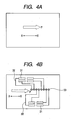
- Fig. 4 is a diagram illustrating a polishing process using buff of Fig. 3.
- a plurality of fixed contacts 31 extending in an X-X direction of Fig. 1, lead conductors 32 extending from the fixed contacts 31, and terminals 33 connected to ends of the lead conductors 32 are formed in a pattern on a circuit board 30 according to the first embodiment, and a non-contact region except for the fixed contacts 31 and the terminals 33 is covered with a solder resist 34 that is formed of an insulating material.
- Each of the fixed contacts 31 is formed by plating a cooper foil with nickel and then plating the nickel-plated layer with gold (pure gold), and the uppermost gold layer serves as a sliding contact surface with a movable contact, which will be described later. As shown in Fig.
- a movable contact 35 is provided on a lower surface of a sliding-element supporting member 36 by, for example, caulking, and the sliding-element supporting member 36 is moved on the circuit board 30 in the X-X direction such that the movable contact 35 slides on the surface of the fixed contacts 31.
- the movable contact 35 is formed by cladding one surface of an elastic metal plate formed of phosphor bronze with a gold alloy.
- the movable contact 35 is formed of a gold alloy containing 75% or more of precious metal, such as gold or platinum (for example, a quinary alloy of Au, Pt, Ag, Ni, and Cu), considering corrosion resistance and hardness.
- a process of manufacturing the circuit board 30 having the above-mentioned structure will be described with reference to Fig. 3.
- a copper-clad insulating substrate formed by cladding one surface or both surfaces of an epoxy resin containing glass with copper is prepared (S-1), and the surface of the copper-clad insulating substrate is polished with buff to remove an oxide film from the surface of the cooper foil (S-2).
- the buffing direction P is aligned with the X-X direction, which is the sliding direction of the movable contact 35.
- a resist is coated on the entire surface of the cooper foil, and the coated resist is partially exposed and removed.
- the copper foil is etched in a desired shape, thereby forming the patterns of the fixed contacts 31, the lead conductors 32, and the terminals 33 (S-3).
- the surface of the copper-clad insulating substrate is polished with buff to remove an oxide film adhered on the surface of the copper foil (the fixed contacts 31 or the terminals 33) (S-4).
- the buffing direction P is aligned with the X-X direction, which is the sliding direction of the movable contact 35.
- solder resist 34a is coated on a specific region on the insulating substrate except for the fixed contacts 31 and the terminals 33 (S-5), and a nickel layer having a thickness of about 2 ⁇ m and a gold layer having a thickness of about 0.05 ⁇ m are sequentially formed on the fixed contacts 31s and the terminals 33 by plating (S-6).
- the circuit board 30 manufactured through the above-mentioned processes has a contact structure having high environmental characteristics including a measure to sulfurization.
- the buffing direction P is aligned with the sliding direction of the movable contact 35 during the buffing processes (S-2 and S-4), an uneven portion that occurs in the surface of the gold layer due to the buffing process in the subsequent plating process (S-6) does not cause the scraping of the movable contact 35 or the fixed contact 31.
- the nickel layer since a nickel layer having a thickness of 1 ⁇ m or less cannot sufficiently serve as a base layer, the nickel layer may have a thickness of 1 to 5 ⁇ m, preferably, about 2 ⁇ m. Since gold used for gold plating is expensive and has high malleability, the gold layer may have a thickness of 0.01 to 0.5 ⁇ m, preferably, about 0.05 ⁇ m.
- the fixed contacts 31 are plated with pure gold, and the movable contact 35 is plated with a gold alloy. Therefore, the hardness of the movable contact 35 is higher than the hardness of the fixed contact 31. This is because, when the movable contact 35 moves, a contact point on the fixed contact 31 with the movable contact 35 is changed, but a contact point on the movable contact 35 with the fixed contact 31 is not changed.
- the fixed contact 31 is plated with pure gold
- the movable contact 35 is formed of a clad material.
- the fixed contact may be formed of a material containing 0.1% to several percent of additive, such as cobalt, nickel, silver, or indium to improve the hardness, and the movable contact may be plated with gold.
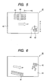
- Fig. 5 is a plan view illustrating a circuit board according to a second embodiment of the invention.
- First fixed contacts 41a extending in parallel to a long side of a rectangular insulating substrate and second fixed contacts 42 extending substantially in parallel to a short side of the insulating substrate are patterned on a circuit board 40, and a non-contact region except for the first and second fixed contacts 41 and 42 is covered with a solder resist 43 formed of an insulating material.
- the first and second fixed contacts 41 and 42 are obtained by sequentially forming a nickel layer having a thickness of 2 ⁇ m and a gold layer having a thickness of 0.05 ⁇ m on a copper foil, which is a raw material, by plating.
- the gold layer which is an uppermost layer of the first fixed contact 41, serves as a contact surface with a first movable contact 44
- the gold layer which is an uppermost layer of the second fixed contact 42
- the first movable contact 44 is mounted to a sliding-element supporting member (not shown) so as to be movable on the first fixed contact 41 in an X-X direction
- the second movable contact 45 is mounted to a sliding-element supporting member (not shown) so as to be movable on the second fixed contact 42 in a direction that is substantially parallel to a Y-Y direction.
- the first movable contact 44 requiring a long life span is plated with a gold alloy, similar to the first embodiment.
- the second movable contact 45 having a shorter life span than the first movable contact 44 may be plated with a gold alloy, similar to the first movable contact 44.
- the second movable contact 45 may be plated with gold or silver, or it may be formed of a silver-clad material. In this case, manufacturing costs can be reduced.
- the circuit board 40 having the above-mentioned structure is manufactured through the processes shown in Fig. 3, similar to the first embodiment.
- the buffing direction P is aligned with the sliding direction (X-X direction) of the first movable contact 44, and the buffing direction P is substantially vertical to the sliding direction (substantially in the Y-Y direction) of the second movable contact 45.
- a plating process S-6 in Fig.
- Fig. 6 is a plan view illustrating a circuit board according to a third embodiment of the invention.
- the same components as those shown in Fig. 5 are denoted by the same reference numerals.
- the structure of a circuit board 50 shown in Fig. 6 is similar to that of the circuit board 40 according to the second embodiment except that the first fixed contact 41 extends in a direction that is slightly inclined with respect to a long side of an insulating substrate.
- the following method may be performed to obtain a plurality of circuit boards 50: a plurality of first fixed contacts 41 are collectively patterned on the surface of a large insulating substrate so as to extend in the same direction; a buffing process is performed on the large insulating substrate with a buffing direction P being aligned with the direction in which the first fixed contacts 41 extend; a plating process is performed on the large insulating substrate; and the large insulating substrate is divided into a plurality of circuit boards 50.
- Fig. 7 is an exploded perspective view illustrating a turn signal switch device according to this embodiment of the invention.
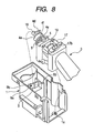
- Fig. 8 is a perspective view illustrating an operating level encased into a first case provided in the turn signal switch device
- Fig. 9 is a transverse cross-sectional view illustrating the turn signal switch device
- Fig. 10 is a longitudinal cross-sectional view illustrating the turn signal switch device.
- Fig. 11 is a front view illustrating a rotating member provided in the turn signal switch device
- Figs. 12A and 12B are diagrams illustrating a cancel operation of the turn signal switch device.
- the turn signal switch device includes first and second cases 1 and 2 that are integrally coupled to each other to form a housing, an operating lever 3 that is rotatably supported by the two cases 1 and 2, a rotating member 4 that is rotatably supported by the operating lever 3, a return spring 5 that automatically returns the rotating member 4 to its central position, first and second lever members 6 and 7 that are mounted on an upper surface of the second case 2, and a twist coil spring 8 that elastically urges the second lever member 7 in a direction in which the second lever member 7 protrudes from the second case 2.
- the first and second cases 1 and 2 are fixed to a column cover or a stator member, such as a combination switch (not shown).
- a V-shaped cam surface 9 is formed inside the first case 1, and the cam surface 9 includes a central valley portion 9a and protruding lock portions 9b provided at both sides of the valley portion 9a.
- the first case 1 and the second case 2 are integrated into one body by, for example, a snapping connection unit, and holes 1a and 2a, which are rotating points of the operating lever 3, are formed in the two cases 1 and 2, respectively.
- a first support pin 10 and a second support pin 11 are provided at a predetermined interval on the inner bottom surface of the second case 2, and a first lever member 6 is rotatably supported by the first support pin 10.
- a first clearance hole 12 and a second clearance hole 13 are formed in the first lever member 6, and a hole 6a to which the first support pin 10 is fitted is formed between the two clearance holes 12 and 13.
- a support pin 6b is provided at a leading end of the first lever member 6, and the second lever member 7 is rotatably supported by the support pin 6b.
- a first long hole 7a to which the support pin 6b is fitted and a second long hole 7b to which the second support pin 11 is fitted are formed in the second lever member 7 such that the longitudinal directions of the two holes 7a and 7b are collinear.
- an abutting portion 7c and a cam portion 7d are formed at front and rear ends of the second lever member 7, respectively, and the cam portion 7d has a semicircular shape in sectional view.
- One end of the twist coil spring 8 is retained in the second lever member 7, and the twist coil spring 8 elastically urges the second lever member 7 in the longitudinal directions of the two holes 7a and 7b.
- a winding portion of the twist coil spring 8 is fitted to a boss 2b formed on the inner bottom surface of the second case 2, and the other end of the twist coil spring 8 is retained in the side wall of the second case 2.
- a step portion 2c and a rib 2d abutting on the bottom surface of the second lever member 7 are formed on the inner bottom surface of the second case 2. The step portion 2c and the rib 2d reduce contact resistance between the second case 2 and the second lever member 7.
- a circuit board 14 is mounted on the bottom of the second case 2, and is substantially equivalent to the circuit board 40 according to the second embodiment. That is, first fixed contacts 21 and second fixed contacts 22 are formed on the surface of the circuit board 14 such that their extending directions are substantially orthogonal to each other, and the first and second fixed contacts 21 and 22 are plated with gold.
- the first fixed contact 21 is a fixed contact for a winker operation that requires a long life span, and during a buffing process, a buffing direction is aligned with a direction in which the first fixed contacts 21 extend (a direction in which a first movable contact 23, which will be described later, slides).
- a first sliding-element supporting member 15 and a second sliding-element supporting member 16 are provided between the bottom of the second case 2 and the circuit board 14, and the first movable contact 23 sliding on the first fixed contact 21 is provided on a lower surface of the sliding-element supporting member 15.
- the first movable contact 23 is formed by plating or cladding one surface of an elastic metal plate made of phosphor bronze with a gold alloy, and thus the life span of the switch device can be improved by the synergetic effect of the first fixed contact 21 plated with gold and the first movable contact 23 plated with a gold alloy.
- a driving support member 15a protrudes from the upper surface of the first sliding-element supporting member 15, and the driving support member 15a is exposed toward the inner bottom surface of the second case 2.
- the first sliding-element supporting member 15 is movable in the direction in which the first fixed contact 21 extends, and as will be described later, the first sliding-element supporting member 15 is driven by a left turn operation or a light turn operation of the operating lever 3 to turn on or off a left turn lamp or a light turn lamp (not shown) (winder operation).
- the second fixed contact 22 is a fixed contact for a passing operation, and the second movable contact 24 sliding on the second fixed contact 22 is provided on the lower surface of the second sliding-element supporting member 16. Since a contact structure for the passing operation does not require a longer life span than that for the winder operation, the second movable contact 24 is plated or clad with silver, considering manufacturing costs.
- a driving support member 16a is provided on the surface of the second sliding-element supporting member 16 so as to protrude therefrom, and the driving support member 16a is also exposed toward the inner bottom surface of the second case 2.
- the second sliding-element supporting member 16 is movable in the direction in which the second fixed contact 22 extends. As will be described later, when the operating lever 3 is operated upward, the second sliding-element supporting member 16 is driven to turn on a beam lamp (not shown) (passing operation).
- a holder 17 is mounted on the operating lever 3, and support pins 17a and 17b fitted to the two holes 1a and 2a are provided on the upper and lower surfaces of the holder 17, respectively.
- the operating lever 3 and the holder 17 integrally rotate in the horizontal direction on a rotating axis linking the two holes 1a and 2a (two support pins 17a and 17b) in a straight line.
- the operating lever 3 is connected to the holder 17 such that it can rock by a predetermined angle in the vertical direction of the holder 17 by a beam driving mechanism (not shown).
- a pair of spring bearings 17c and 17d are formed on the upper surface of the holder 17, and a cylindrical portion 17e is formed on a front surface of the holder 17.
- a driving member 18 is slidably provided inside the cylindrical portion 17e, and a leading end of the driving member 18 is brought into pressure contact with the cam surface 9 of the first case 1 by a spring (not shown) at all times.
- the cylindrical portion 17e of the holder 17 is fitted to a tubal member 4a formed on the rotating member 4, and the rotating member 4 is rotatably maintained in the holder 17 using the cylindrical portion 17e as a guide surface (see Fig. 11).
- a pair of spring bearings 4b and 4c are formed at an upper part of the rotating member 4, and both ends of the return spring 5 wound around the tubal member 4a are retained in the two spring bearings 4b and 4c and the two spring bearings 17c and 17d of the holder 17, so that the rotating member 4 is urged toward the central position at all times.
- a cam portion 4d extends downward from the lower end of the tuba member 4a in a semicircular shape in sectional view.
- the cam portion 4d is opposite to the cam portion 7d of the second lever member 7.
- a driving portion 4e extends downward from the lower end of the rotating member 4 to reach the second clearance hole 13 of the first lever member 6, and a protrusion 4f engaged with the driving support member 15a of the first sliding-element supporting member 15 is formed on the driving portion 4e.
- a protrusion 19 is formed at a lower end of the operating lever 3, and the protrusion 19 is engaged with the driving support member 16a of the second sliding-element supporting member 16.
- the abutting portion 7c of the second lever member 7 is disposed outside the rotating locus of a cancel protrusion 20 provided in a rotor that rotates so as to be operatively associated with the rotation of a steering wheel. Therefore, even when the steering wheel rotates in this state, the cancel protrusion 20 does not contact with the abutting portion 7c of the second lever member 7, and the operating lever 3 is kept at the neutral position.
- the cam portion 7d of the second lever member 7 rotatably slides on the peripheral surface of the cam portion 4d of the rotating member 4 smoothly, and the first lever member 6 rotates in the direction in which the periphery of the second clearance hole 13 is separated from the driving portion 4e.
- the operating lever 3 is maintained at the right turn position without being returning to the neutral position.
- the operating lever 3 When the operating lever 3 is operated from the neutral position to the upper side, the operating lever 3 rocks in the vertical direction of the holder 17 by a beam driving mechanism (not shown), and the protrusion 19 provided at the lower part of the operating lever 3 moves the second sliding-element supporting member 16. Then, the second movable contact 24 provided on the lower surface of the second sliding-element supporting member 16 slides on the second fixed contact 22, so that contact switching is performed. As a result, a beam lamp (not shown) is turned on.
- the first fixed contact 21 for a winker operation and the second fixed contact 22 for a passing operation are provided on the same surface of the circuit board 14.
- the buffing direction is substantially aligned with the direction in which the first movable contact 23 slides on the first fixed contact 21.
- the first fixed contact 21 for a winker operation and the second fixed contact 22 for a passing operation are provided on the circuit board 14 so as to be substantially orthogonal to each other.
- the first and second fixed contacts may extend in the same direction, that is, the first and second movable contacts may slide in the same direction.
- the buffing direction may be aligned with the sliding direction of the first and second movable contacts.
- the circuit board is applied to a turn signal switch device, but the invention is not limited thereto.
- the circuit board according to the embodiments of the invention can be applied to a switch device that has fixed contacts formed in a copper foil pattern and requires a long life span, such as a switch device for gearshift.
Landscapes
- Chemical & Material Sciences (AREA)
- Engineering & Computer Science (AREA)
- Organic Chemistry (AREA)
- Chemical Kinetics & Catalysis (AREA)
- Materials Engineering (AREA)
- Metallurgy (AREA)
- Electrochemistry (AREA)
- Mechanical Engineering (AREA)
- Manufacturing & Machinery (AREA)
- Microelectronics & Electronic Packaging (AREA)
- Switches With Compound Operations (AREA)
- Contacts (AREA)
- Manufacture Of Switches (AREA)
- Manufacturing Of Printed Wiring (AREA)
Abstract
Description
- The present invention relates a method of manufacturing a circuit board used for various switch devices, and more particularly, to a method of manufacturing a circuit board used for a slide-type switch device in which a movable contact slides on a fixed contact.
- In general, in a method of manufacturing a circuit board used for a slide-type switch device, first, a copper-clad insulating substrate formed by cladding one surface or both surfaces of an epoxy resin containing glass with copper is prepared, and the copper foil is etched to form fixed contact and lead conductor patterns. Then, a solder resist is coated on a specific region on the insulating substrate except for the fixed contact, and a nickel layer (a thickness of about 2 µm) and a silver layer (a thickness of about 5 µm) are sequentially formed on the fixed contact by plating. In the manufacturing method, when an oxide film remains on the surface of the copper foil during the etching process and the process of coating the solder resist, the adhesion of a resist or a solder resist used for etching is considerably reduced. Therefore, a process of polishing the surface of the copper foil with buff is additionally performed before the etching process and the solder resist coating process to remove the oxide film from the surface of the copper foil (for example, see
Japanese Utility Model Application Laid-Open No. 6-77277 - In the circuit board manufactured through the above-mentioned processes, since the total sum of the thicknesses of the nickel layer (base layer) and the silver layer formed on the copper foil, which is a raw material forming the fixed contact, is about 7 µm, it is possible to planarize the silver layer, which is the uppermost layer of the fixed contact, and thus to length the life span of the fixed contact and a movable contact sliding thereon. However, this structure has a problem in that the silver layer is sulfurized, which may cause the reliability of electrical connection to be lowered. Therefore, a switch device requiring a long life span and high reliability, for example, a vehicle-mounted turn signal switch device or steering switch device that needs to be used hundreds of thousands of times is plated with gold not sulfurized, instead of silver. In this case, a gold layer is formed on the nickel layer, which is a base layer, with a predetermined thickness by plating. However, since gold is considerably more expensive than silver and has high malleability, the thickness of the gold layer is generally set to about 0.05 µm.
- As described above, in the circuit board having the gold layer as the uppermost layer of the fixed contact, since the uppermost layer of the fixed contact is plated with gold not sulfurized, the reliability of electrical connection is improved, but a sufficiently long life span is not obtained. The inventors' study proved that a strip-shaped uneven portion occurs in the surface of the gold layer, and when the sliding direction of a movable contact is orthogonal to the direction in which the uneven portion extends, the abrasion loss of the fixed contact and the movable contact increases due to the uneven portion. The uneven portion occurs in the surface of the gold layer due to scars occurring in the surface of the copper foil during a polishing process using buff. That is, in a thick laminated structure of the nickel layer and the silver layer having a thickness of about 7 µm, since a thick nickel layer is formed on the uneven portion occurring due to the scars caused by the buffing process, little unevenness occurs in the surface of the uppermost layer. However, in a thin gold layer having a thickness of about 2 µm, unevenness occurs in the surface of the gold layer due to the scars occurring in the surface of the copper foil during the buffing process. This is because, regardless of the direction in which the surface extends, a plated layer tends to be substantially uniformly formed in a direction orthogonal to the surface and the gap between the surfaces of both sides of one concave portion becomes narrower when the plated layer is formed. In particular, when new buff having a sharp leading end is used, the depth of the scars caused by the buffing process increases, which causes the depth of an uneven portion occurring in the surface of the gold layer to increase. As a result, the abrasion of the fixed contact or the movable contact is accelerated.
- The invention has been finalized to solve the problems of the related art, and an object of the invention is to provide a method of manufacturing a circuit board capable of improving the reliability of electrical connection, reducing the abrasion loss of a fixed contact and a movable contact, and lengthening the life span of the fixed contact and the movable contact by plating the fixed contact with gold.
- In order to achieve the above-mentioned object, according to an aspect of the invention, there is provided a method of manufacturing a circuit board having fixed contacts on which a movable contact slides. The method includes: etching a copper foil formed on the entire surface of an insulating substrate to form the pattern of the fixed contact; polishing the surface of the copper foil with buff; and sequentially forming a nickel layer having a thickness of 1 to 5 µm and a gold layer having a thickness of 0.01 to 0.5 µm on the fixed contacts. In the method, the buffing direction is substantially aligned with a sliding direction of the movable contact.
- In the process of polishing the surface of the copper foil, which is a raw material forming the fixed contacts, with buff, when the buffing direction is substantially aligned with the sliding direction of the movable contact, an uneven portion that occurs in the surface of the gold layer due to scars caused by the buffing process in a subsequent plating process does not cause the scraping of the movable contact or the fixed contact. Therefore, when the fixed contact is plated with gold, the reliability of electrical connection is improved, and the abrasion loss of the fixed contact or the movable contact is reduced, which makes it possible to lengthen the life span of the fixed contact or the movable contact.
- In this case, the movable contact sliding on the fixed contacts may be plated with silver, or it may be formed of a silver-clad material. When the movable contact is formed by plating or cladding one surface of an elastic metal plate with gold or a gold alloy, the life span of the movable contact can be further improved by the synergetic effect of the gold layer of the fixed contact and the gold alloy later of the movable contact.
- Further, in order to achieve the above-mentioned object, according to another aspect of the invention, there is provided a method of manufacturing a circuit board having first and second fixed contacts formed on the same surface, in which first and second movable contacts respectively slide on the first and second fixed contacts so as to be substantially orthogonal to each other. The method includes: etching a copper foil formed on the entire surface of an insulating substrate to form the patterns of the first and second fixed contacts; polishing the surface of the copper foil with buff; and sequentially forming a nickel layer having a thickness of 1 to 5 µm and a gold layer having a thickness of 0.01 to 0.5 µm on each of the first and second fixed contacts. In the method, the buffing direction is substantially aligned with a direction in which the first movable contact slides on the first fixed contact.
- In the process of manufacturing the circuit board having the first and second fixed contacts that extend substantially orthogonal to each other, in which the first and second movable contacts respectively slide on the first and second fixed contacts so as to be substantially orthogonal to each other, when the surface of the copper foil, which is a raw material forming the first and second fixed contacts, is polished with buff substantially in the same direction in which the first movable contact slides on the first fixed contact, an uneven portion that occurs in the surface of the gold layer, which is the uppermost layer of each of the first and second fixed contacts, due to scars caused by the buffing process in a subsequent plating process does not cause the scraping of the first movable contact sliding on the first fixed contact. Therefore, when the first and second fixed contacts are plated with gold, the reliability of electrical connection is improved, and the abrasion loss of the first fixed contact or the first movable contact is reduced, which makes it possible to lengthen the life span of the first fixed contact or the first movable contact. In this case, the abrasion loss of the second movable contact sliding on the second fixed contact increases due to the uneven portion occurring in the surface of the gold layer of the second fixed contact. However, when a contact structure requiring a shorter life span than that of the first fixed contact is applied to the second fixed contact, it is possible to improve the overall reliability of a switch device and lengthen the life span thereof.
- A turn signal switch device may be used as the switch device. In this case, when the first fixed contact is used as a contact for a winker operation of the turn signal switch device and the second fixed contact is used as a contact for a passing operation of the turn signal switch device, it is possible to lengthen the life span of a contact structure for the winker operation that is more frequently used than that for the passing operation, and thus provide a turn signal switch device having high reliability of electrical connection and a long life span.
- In a method of manufacturing a circuit board according to an embodiment of the invention, since the surface of a copper foil, which is a raw material forming a fixed contact, is polished with buff substantially in the same direction in which a movable contact slides on the fixed contact, an uneven portion that occurs in the surface of a gold layer, which is the uppermost layer of the fixed contact, due to scars caused by the buffing process in a subsequent plating process does not cause the scraping of the movable contact or the fixed contact. Therefore, when the fixed contact is plated with gold, the reliability of electrical connection is improved, and the abrasion loss of the fixed contact or the movable contact is reduced, which makes it possible to lengthen the life span of the fixed contact or the movable contact.
-
- Fig. 1 is a plan view illustrating a circuit board according to a first embodiment of the invention;
- Fig. 2 is a diagram illustrating contact between the circuit board and a movable contact;
- Fig. 3 is a flow chart illustrating a process of manufacturing the circuit board;
- Fig. 4 is a diagram illustrating a buffing process of Fig. 3;
- Fig. 5 is a plan view illustrating a circuit board according to a second embodiment of the invention;
- Fig. 6 is a plan view illustrating a circuit board according to a third embodiment of the invention;
- Fig. 7 is an exploded perspective view illustrating a turn signal switch device according to an embodiment of the invention;
- Fig. 8 is a perspective view illustrating an operating lever encased in a first case of the turn signal switch device;
- Fig. 9 is a transverse cross-sectional view illustrating the turn signal switch device;
- Fig. 10 is a longitudinal cross-sectional view illustrating the turn signal switch device;
- Fig. 11 is a front view illustrating a rotating member provided in the turn signal switch device; and
- Fig. 12 is a diagram illustrating a cancel operation of the turn signal switch device.
- Hereinafter, exemplary embodiments of the invention will be described with reference to the accompanying drawings. Fig. 1 is a plan view illustrating a circuit board according to a first embodiment of the invention. Fig. 2 is a diagram illustrating contact between the circuit board and a movable contact. Fig. 3 is a flow chart illustrating a process of manufacturing the circuit board. Fig. 4 is a diagram illustrating a polishing process using buff of Fig. 3.
- As show in Fig. 1, a plurality of
fixed contacts 31 extending in an X-X direction of Fig. 1,lead conductors 32 extending from thefixed contacts 31, andterminals 33 connected to ends of thelead conductors 32 are formed in a pattern on acircuit board 30 according to the first embodiment, and a non-contact region except for thefixed contacts 31 and theterminals 33 is covered with asolder resist 34 that is formed of an insulating material. Each of thefixed contacts 31 is formed by plating a cooper foil with nickel and then plating the nickel-plated layer with gold (pure gold), and the uppermost gold layer serves as a sliding contact surface with a movable contact, which will be described later. As shown in Fig. 2, amovable contact 35 is provided on a lower surface of a sliding-element supporting member 36 by, for example, caulking, and the sliding-element supporting member 36 is moved on thecircuit board 30 in the X-X direction such that themovable contact 35 slides on the surface of thefixed contacts 31. In addition, themovable contact 35 is formed by cladding one surface of an elastic metal plate formed of phosphor bronze with a gold alloy. In this embodiment, themovable contact 35 is formed of a gold alloy containing 75% or more of precious metal, such as gold or platinum (for example, a quinary alloy of Au, Pt, Ag, Ni, and Cu), considering corrosion resistance and hardness. - Next, a process of manufacturing the
circuit board 30 having the above-mentioned structure will be described with reference to Fig. 3. First, a copper-clad insulating substrate formed by cladding one surface or both surfaces of an epoxy resin containing glass with copper is prepared (S-1), and the surface of the copper-clad insulating substrate is polished with buff to remove an oxide film from the surface of the cooper foil (S-2). As shown in Fig. 4A, in the buffing process, when buffing is performed in the direction of an arrow P, the buffing direction P is aligned with the X-X direction, which is the sliding direction of themovable contact 35. Then, a resist is coated on the entire surface of the cooper foil, and the coated resist is partially exposed and removed. Then, the copper foil is etched in a desired shape, thereby forming the patterns of the fixedcontacts 31, thelead conductors 32, and the terminals 33 (S-3). Subsequently, the surface of the copper-clad insulating substrate is polished with buff to remove an oxide film adhered on the surface of the copper foil (the fixedcontacts 31 or the terminals 33) (S-4). As shown in Fig. 4B, in the buffing process, the buffing direction P is aligned with the X-X direction, which is the sliding direction of themovable contact 35. Then, a solder resist 34a is coated on a specific region on the insulating substrate except for the fixedcontacts 31 and the terminals 33 (S-5), and a nickel layer having a thickness of about 2 µm and a gold layer having a thickness of about 0.05 µm are sequentially formed on the fixed contacts 31s and theterminals 33 by plating (S-6). - Since the uppermost layer of the copper foil, which is a raw material forming the fixed
contacts 31, is plated with gold, thecircuit board 30 manufactured through the above-mentioned processes has a contact structure having high environmental characteristics including a measure to sulfurization. In addition, since the buffing direction P is aligned with the sliding direction of themovable contact 35 during the buffing processes (S-2 and S-4), an uneven portion that occurs in the surface of the gold layer due to the buffing process in the subsequent plating process (S-6) does not cause the scraping of themovable contact 35 or the fixedcontact 31. Therefore, it is possible to improve the reliability of electrical connection by plating the fixedcontacts 31 with gold, and it is also possible to reduce the abrasion loss of the fixedcontacts 31 or themovable contacts 35, which results in a long life span. In addition, since a nickel layer having a thickness of 1 µm or less cannot sufficiently serve as a base layer, the nickel layer may have a thickness of 1 to 5 µm, preferably, about 2 µm. Since gold used for gold plating is expensive and has high malleability, the gold layer may have a thickness of 0.01 to 0.5 µm, preferably, about 0.05 µm. - In this embodiment, the fixed
contacts 31 are plated with pure gold, and themovable contact 35 is plated with a gold alloy. Therefore, the hardness of themovable contact 35 is higher than the hardness of the fixedcontact 31. This is because, when themovable contact 35 moves, a contact point on the fixedcontact 31 with themovable contact 35 is changed, but a contact point on themovable contact 35 with the fixedcontact 31 is not changed. In addition, since it is difficult to mix gold with impurities in the gold plating, in this embodiment, the fixedcontact 31 is plated with pure gold, and themovable contact 35 is formed of a clad material. However, the invention is not limited thereto, but the fixed contact may be formed of a material containing 0.1% to several percent of additive, such as cobalt, nickel, silver, or indium to improve the hardness, and the movable contact may be plated with gold. - Fig. 5 is a plan view illustrating a circuit board according to a second embodiment of the invention. First fixed contacts 41a extending in parallel to a long side of a rectangular insulating substrate and second
fixed contacts 42 extending substantially in parallel to a short side of the insulating substrate are patterned on acircuit board 40, and a non-contact region except for the first and secondfixed contacts fixed contacts contact 41, serves as a contact surface with a firstmovable contact 44, and the gold layer, which is an uppermost layer of the second fixedcontact 42, serves as a contact surface with a secondmovable contact 45. The firstmovable contact 44 is mounted to a sliding-element supporting member (not shown) so as to be movable on the first fixedcontact 41 in an X-X direction, and the secondmovable contact 45 is mounted to a sliding-element supporting member (not shown) so as to be movable on the second fixedcontact 42 in a direction that is substantially parallel to a Y-Y direction. Since the number of times a contact structure including the firstfixed contacts 41 and the firstmovable contact 44 is used is considerably larger than the number of times a contact structure including the secondfixed contacts 42 and the secondmovable contact 45, the firstmovable contact 44 requiring a long life span is plated with a gold alloy, similar to the first embodiment. However, the secondmovable contact 45 having a shorter life span than the firstmovable contact 44 may be plated with a gold alloy, similar to the firstmovable contact 44. Alternatively, the secondmovable contact 45 may be plated with gold or silver, or it may be formed of a silver-clad material. In this case, manufacturing costs can be reduced. - The
circuit board 40 having the above-mentioned structure is manufactured through the processes shown in Fig. 3, similar to the first embodiment. However, in this embodiment, during the buffing processes (S-2 and S-4 in Fig. 3), the buffing direction P is aligned with the sliding direction (X-X direction) of the firstmovable contact 44, and the buffing direction P is substantially vertical to the sliding direction (substantially in the Y-Y direction) of the secondmovable contact 45. As a result, in a plating process (S-6 in Fig. 3), when uneven portions occur in the gold layers, which are the uppermost layers of the first and secondfixed contacts contact 41 does not cause the scraping of the firstmovable contact 44 that slides on the uneven portion. Therefore, gold plating is performed on the first and secondfixed contacts fixed contacts contact 41 and the firstmovable contact 44 is reduced, which makes it possible to lengthen the life span of the first fixedcontact 41 and the firstmovable contact 44. In this case, since uneven portions occurs in the surface of the gold layer of the second fixedcontact 42 in a direction substantially vertical to the sliding direction of the secondmovable contact 45, the abrasion loss of the secondmovable contact 45 sliding on the second fixedcontact 42 increases slightly. However, as described above, since the second fixedcontact 42 is applied to a contact structure that does not require a longer life span than the first fixedcontact 41, the life span and the reliability of the entire switch device can be improved. - Fig. 6 is a plan view illustrating a circuit board according to a third embodiment of the invention. In Fig. 6, the same components as those shown in Fig. 5 are denoted by the same reference numerals.
- The structure of a
circuit board 50 shown in Fig. 6 is similar to that of thecircuit board 40 according to the second embodiment except that the first fixedcontact 41 extends in a direction that is slightly inclined with respect to a long side of an insulating substrate. In this case, the following method may be performed to obtain a plurality of circuit boards 50: a plurality of first fixedcontacts 41 are collectively patterned on the surface of a large insulating substrate so as to extend in the same direction; a buffing process is performed on the large insulating substrate with a buffing direction P being aligned with the direction in which the firstfixed contacts 41 extend; a plating process is performed on the large insulating substrate; and the large insulating substrate is divided into a plurality ofcircuit boards 50. - Next, a turn signal switch device to which the circuit board according to the embodiments of the invention is applied will be described with reference to Figs. 7 to 12. Fig. 7 is an exploded perspective view illustrating a turn signal switch device according to this embodiment of the invention. Fig. 8 is a perspective view illustrating an operating level encased into a first case provided in the turn signal switch device, Fig. 9 is a transverse cross-sectional view illustrating the turn signal switch device, and Fig. 10 is a longitudinal cross-sectional view illustrating the turn signal switch device. Fig. 11 is a front view illustrating a rotating member provided in the turn signal switch device, and Figs. 12A and 12B are diagrams illustrating a cancel operation of the turn signal switch device.
- As shown in the drawings, the turn signal switch device according to this embodiment includes first and
second cases lever 3 that is rotatably supported by the twocases member 4 that is rotatably supported by the operatinglever 3, areturn spring 5 that automatically returns the rotatingmember 4 to its central position, first andsecond lever members second case 2, and atwist coil spring 8 that elastically urges thesecond lever member 7 in a direction in which thesecond lever member 7 protrudes from thesecond case 2. The first andsecond cases - A V-shaped
cam surface 9 is formed inside thefirst case 1, and thecam surface 9 includes acentral valley portion 9a and protrudinglock portions 9b provided at both sides of thevalley portion 9a. Thefirst case 1 and thesecond case 2 are integrated into one body by, for example, a snapping connection unit, and holes 1a and 2a, which are rotating points of the operatinglever 3, are formed in the twocases first support pin 10 and asecond support pin 11 are provided at a predetermined interval on the inner bottom surface of thesecond case 2, and afirst lever member 6 is rotatably supported by thefirst support pin 10. Afirst clearance hole 12 and asecond clearance hole 13 are formed in thefirst lever member 6, and ahole 6a to which thefirst support pin 10 is fitted is formed between the twoclearance holes support pin 6b is provided at a leading end of thefirst lever member 6, and thesecond lever member 7 is rotatably supported by thesupport pin 6b. - A first
long hole 7a to which thesupport pin 6b is fitted and a secondlong hole 7b to which thesecond support pin 11 is fitted are formed in thesecond lever member 7 such that the longitudinal directions of the twoholes portion 7c and acam portion 7d are formed at front and rear ends of thesecond lever member 7, respectively, and thecam portion 7d has a semicircular shape in sectional view. One end of thetwist coil spring 8 is retained in thesecond lever member 7, and thetwist coil spring 8 elastically urges thesecond lever member 7 in the longitudinal directions of the twoholes twist coil spring 8 is fitted to aboss 2b formed on the inner bottom surface of thesecond case 2, and the other end of thetwist coil spring 8 is retained in the side wall of thesecond case 2. In addition, astep portion 2c and arib 2d abutting on the bottom surface of thesecond lever member 7 are formed on the inner bottom surface of thesecond case 2. Thestep portion 2c and therib 2d reduce contact resistance between thesecond case 2 and thesecond lever member 7. - A
circuit board 14 is mounted on the bottom of thesecond case 2, and is substantially equivalent to thecircuit board 40 according to the second embodiment. That is, firstfixed contacts 21 and secondfixed contacts 22 are formed on the surface of thecircuit board 14 such that their extending directions are substantially orthogonal to each other, and the first and secondfixed contacts contact 21 is a fixed contact for a winker operation that requires a long life span, and during a buffing process, a buffing direction is aligned with a direction in which the firstfixed contacts 21 extend (a direction in which a firstmovable contact 23, which will be described later, slides). A first sliding-element supporting member 15 and a second sliding-element supporting member 16 are provided between the bottom of thesecond case 2 and thecircuit board 14, and the firstmovable contact 23 sliding on the first fixedcontact 21 is provided on a lower surface of the sliding-element supporting member 15. The firstmovable contact 23 is formed by plating or cladding one surface of an elastic metal plate made of phosphor bronze with a gold alloy, and thus the life span of the switch device can be improved by the synergetic effect of the first fixedcontact 21 plated with gold and the firstmovable contact 23 plated with a gold alloy. A drivingsupport member 15a protrudes from the upper surface of the first sliding-element supporting member 15, and the drivingsupport member 15a is exposed toward the inner bottom surface of thesecond case 2. The first sliding-element supporting member 15 is movable in the direction in which the first fixedcontact 21 extends, and as will be described later, the first sliding-element supporting member 15 is driven by a left turn operation or a light turn operation of the operatinglever 3 to turn on or off a left turn lamp or a light turn lamp (not shown) (winder operation). The second fixedcontact 22 is a fixed contact for a passing operation, and the secondmovable contact 24 sliding on the second fixedcontact 22 is provided on the lower surface of the second sliding-element supporting member 16. Since a contact structure for the passing operation does not require a longer life span than that for the winder operation, the secondmovable contact 24 is plated or clad with silver, considering manufacturing costs. A drivingsupport member 16a is provided on the surface of the second sliding-element supporting member 16 so as to protrude therefrom, and the drivingsupport member 16a is also exposed toward the inner bottom surface of thesecond case 2. The second sliding-element supporting member 16 is movable in the direction in which the second fixedcontact 22 extends. As will be described later, when the operatinglever 3 is operated upward, the second sliding-element supporting member 16 is driven to turn on a beam lamp (not shown) (passing operation). - A
holder 17 is mounted on the operatinglever 3, andsupport pins holes holder 17, respectively. The operatinglever 3 and theholder 17 integrally rotate in the horizontal direction on a rotating axis linking the twoholes support pins lever 3 is connected to theholder 17 such that it can rock by a predetermined angle in the vertical direction of theholder 17 by a beam driving mechanism (not shown). A pair ofspring bearings holder 17, and acylindrical portion 17e is formed on a front surface of theholder 17. A drivingmember 18 is slidably provided inside thecylindrical portion 17e, and a leading end of the drivingmember 18 is brought into pressure contact with thecam surface 9 of thefirst case 1 by a spring (not shown) at all times. - The
cylindrical portion 17e of theholder 17 is fitted to atubal member 4a formed on the rotatingmember 4, and the rotatingmember 4 is rotatably maintained in theholder 17 using thecylindrical portion 17e as a guide surface (see Fig. 11). A pair ofspring bearings member 4, and both ends of thereturn spring 5 wound around thetubal member 4a are retained in the twospring bearings spring bearings holder 17, so that the rotatingmember 4 is urged toward the central position at all times. In addition, acam portion 4d extends downward from the lower end of thetuba member 4a in a semicircular shape in sectional view. Thecam portion 4d is opposite to thecam portion 7d of thesecond lever member 7. In addition, a drivingportion 4e extends downward from the lower end of the rotatingmember 4 to reach thesecond clearance hole 13 of thefirst lever member 6, and aprotrusion 4f engaged with the drivingsupport member 15a of the first sliding-element supporting member 15 is formed on the drivingportion 4e. Aprotrusion 19 is formed at a lower end of the operatinglever 3, and theprotrusion 19 is engaged with the drivingsupport member 16a of the second sliding-element supporting member 16. - Next, the operation of the turn signal switch device having the above-mentioned structure will be described below. First, as shown in Fig. 9, when the operating
lever 3 is at a neutral position, the drivingmember 18 is stably maintained at a predetermined position by the elasticity of a spring (not shown) with the leading end thereof abutting on thecentral valley portion 9a of thecam surface 9. At that time, as shown in Fig. 12A, thecam portion 4d of the rotatingmember 4 and thecam portion 7d of thesecond lever member 7 come into contact with each other at their vertexes, and thesecond lever member 7 is urged backward by the urging force of thetwist coil spring 8. The abuttingportion 7c of thesecond lever member 7 is disposed outside the rotating locus of a cancelprotrusion 20 provided in a rotor that rotates so as to be operatively associated with the rotation of a steering wheel. Therefore, even when the steering wheel rotates in this state, the cancelprotrusion 20 does not contact with the abuttingportion 7c of thesecond lever member 7, and the operatinglever 3 is kept at the neutral position. - When the operating
lever 3 is operated from the neutral position to the direction of an arrow A or B as shown in Fig. 9, the leading end of the drivingmember 18 goes up an inclined plane of thecam surface 9 and is then engaged with thelock portion 9b. As a result, the drivingmember 18 is stably maintained at a predetermined position by thelock portion 9b. For example, when the operatinglever 3 is operated in the direction of the arrow B in Fig. 9, the rotatingmember 4 operatively associated with the operatinglever 3 is rotated, and thecam portion 4d and the drivingportion 4e that are hatched in Fig. 12 are displaced from a position shown in Fig. 12A to a position shown in Fig. 12B. As a result, thecam portion 4d of the rotatingmember 4 deviates from the vertex of thecam portion 7d of thesecond lever member 7, and the elastic force of thetwist coil spring 8 is applied to thesecond lever member 7 such that thesecond lever member 7 moves forward along the longitudinal direction of the twolong holes portion 7c advances within the rotating locus of the cancelprotrusion 20. In addition, when the operatinglever 3 is operated in the direction of the arrow B, theprotrusion 4f provided at the lower end of the rotatingmember 4 moves the first sliding-element supporting member 15. Therefore, the firstmovable contact 23 mounted on the lower surface of the first sliding-element supporting member 15 slides on the first fixedcontact 21, so that contact switching is performed. As a result, a right turn signal lamp (not shown) is turned on and off. - When the steering wheel rotates in the opposite direction (in the direction of the arrow in Fig. 12B) with the operating lever being disposed at a right turn position shown in Fig. 12B, the cancel
protrusion 20 comes into contact with the abuttingportion 7c of thesecond lever member 7 during the return operation. As a result, thesecond lever member 7 rotates on thesecond support pin 11 in the clockwise direction of Fig. 12B, and then thefirst lever member 6 having thesupport pin 6b that is fitted to the firstlong hole 7a rotates on thefirst support pin 10 in the clockwise direction. Therefore, thesecond clearance hole 13 of thefirst lever member 6 rotates upward in Fig. 12B. Then, the periphery of thesecond clearance hole 13 presses the drivingportion 4e of the rotatingmember 4 upward, so that the drivingmember 18 deviates from thelock portion 9b of thecam surface 9 and moves to thecentral valley portion 9a. As a result, the operatinglever 3 and the first andsecond lever members - When a user rotates the steering wheel in the opposite direction while pressing the
operating lever 3 in the state shown in Fig. 12B, as described above, the periphery of thesecond clearance hole 13 presses the drivingportion 4e of the rotatingmember 4, but the operatinglever 3 is not automatically returned to the neutral position since it is being pressed. In this case, the rotatingmember 4 resists the elastic force of thereturn spring 5 and rotates around a circumferential surface of thecylindrical portion 17e. When the cancelprotrusion 20 passes through the abuttingportion 7c of thesecond lever member 7, the rotatingmember 4 is automatically returned to the central position of theholder 17 by thereturn spring 5, so that theoperating level 3 is maintained at the right turn position shown in Fig. 12B. As described above, since the rotation of thefirst lever member 6 accompanied by the cancellation operation is absorbed by the rotation of the rotatingmember 4, it is possible to prevent the damage of constituent parts of a power transmission system including the twolevers portion 4e. In addition, when the steering wheel is further rotated in the clockwise direction with the operating lever being disposed at the right turn position shown in Fig. 12B, the cancelprotrusion 20 comes into contact with the abuttingportion 7c of thesecond lever member 7 in the opposite direction of the arrow shown in Fig. 12B, and thesecond lever member 7 and thefirst lever member 6 rotate in the counterclockwise direction on the contrary to the cancel operation. In this case, thecam portion 7d of thesecond lever member 7 rotatably slides on the peripheral surface of thecam portion 4d of the rotatingmember 4 smoothly, and thefirst lever member 6 rotates in the direction in which the periphery of thesecond clearance hole 13 is separated from the drivingportion 4e. As a result, the operatinglever 3 is maintained at the right turn position without being returning to the neutral position. - When the operating
lever 3 is operated from the neutral position to the upper side, the operatinglever 3 rocks in the vertical direction of theholder 17 by a beam driving mechanism (not shown), and theprotrusion 19 provided at the lower part of the operatinglever 3 moves the second sliding-element supporting member 16. Then, the secondmovable contact 24 provided on the lower surface of the second sliding-element supporting member 16 slides on the second fixedcontact 22, so that contact switching is performed. As a result, a beam lamp (not shown) is turned on. - In the turn signal switch device according to this embodiment, the first fixed
contact 21 for a winker operation and the second fixedcontact 22 for a passing operation are provided on the same surface of thecircuit board 14. When the surface of a copper foil, which is a raw material forming the first and secondfixed contacts movable contact 23 slides on the first fixedcontact 21. As a result, it is possible to lengthen the life span of a contact structure for a winker operation that is more frequently used than a contact structure for a passing operation. - In the above-described embodiment, the first fixed
contact 21 for a winker operation and the second fixedcontact 22 for a passing operation are provided on thecircuit board 14 so as to be substantially orthogonal to each other. However, the first and second fixed contacts may extend in the same direction, that is, the first and second movable contacts may slide in the same direction. In this case, the buffing direction may be aligned with the sliding direction of the first and second movable contacts. When both the first and second movable contacts are formed of a gold alloy, it is possible to lengthen the life span of both a contact structure for a passing operation and a contact structure for a winker operation. - Further, in the above-described embodiments of the invention, the circuit board is applied to a turn signal switch device, but the invention is not limited thereto. For example, the circuit board according to the embodiments of the invention can be applied to a switch device that has fixed contacts formed in a copper foil pattern and requires a long life span, such as a switch device for gearshift.
Claims (4)
- A method of manufacturing a circuit board having fixed contacts on which a movable contact slides, comprising:etching a copper foil formed on the entire surface of an insulating substrate to form the pattern of the fixed contact;polishing the surface of the copper foil with buff; andsequentially forming a nickel layer having a thickness of 1 to 5 µm and a gold layer having a thickness of 0.01 to 0.5 µm on the fixed contacts,wherein the buffing direction is substantially aligned with a sliding direction of the movable contact.
- The method of manufacturing a circuit board according to claim 1,
wherein the movable contact is formed by plating or cladding one surface of an elastic metal plate with a gold alloy. - A method of manufacturing a circuit board having first and second fixed contacts formed on the same surface, first and second movable contacts respectively sliding on the first and second fixed contacts so as to be substantially orthogonal to each other, comprising:etching a copper foil formed on the entire surface of an insulating substrate to form the patterns of the first and second fixed contacts;polishing the surface of the copper foil with buff; andsequentially forming a nickel layer having a thickness of 1 to 5 µm and a gold layer having a thickness of 0.01 to 0.5 µm on each of the first and second fixed contacts,wherein the buffing direction is substantially aligned with a direction in which the first movable contact slides on the first fixed contact.
- The method of manufacturing a circuit board according to claim 3,
wherein the first fixed contact is a contact for a winker operation of a turn signal switch device, and the second fixed contact is a contact for a passing operation of the turn signal switch device.
Applications Claiming Priority (1)
| Application Number | Priority Date | Filing Date | Title |
|---|---|---|---|
| JP2006284097A JP4374366B2 (en) | 2006-10-18 | 2006-10-18 | Circuit board manufacturing method used in switch device |
Publications (3)
| Publication Number | Publication Date |
|---|---|
| EP1915039A2 true EP1915039A2 (en) | 2008-04-23 |
| EP1915039A3 EP1915039A3 (en) | 2009-07-29 |
| EP1915039B1 EP1915039B1 (en) | 2012-01-18 |
Family
ID=39047477
Family Applications (1)
| Application Number | Title | Priority Date | Filing Date |
|---|---|---|---|
| EP07020024A Not-in-force EP1915039B1 (en) | 2006-10-18 | 2007-10-12 | Method of manufacturing circuit board |
Country Status (4)
| Country | Link |
|---|---|
| US (1) | US7922918B2 (en) |
| EP (1) | EP1915039B1 (en) |
| JP (1) | JP4374366B2 (en) |
| CN (1) | CN100596259C (en) |
Cited By (5)
| Publication number | Priority date | Publication date | Assignee | Title |
|---|---|---|---|---|
| WO2012154374A1 (en) * | 2011-05-09 | 2012-11-15 | Tyco Electronics Corporation | Corrosion resistant electrical conductor |
| FR2982994A1 (en) * | 2011-11-21 | 2013-05-24 | Sc2N Sa | ELECTRIC CONTACT SWITCH |
| US9224550B2 (en) | 2012-12-26 | 2015-12-29 | Tyco Electronics Corporation | Corrosion resistant barrier formed by vapor phase tin reflow |
| EP3975672A1 (en) * | 2020-09-23 | 2022-03-30 | Molto Luce GmbH | Illumination device |
| CN117601442A (en) * | 2023-11-10 | 2024-02-27 | 浙江晶引电子科技有限公司 | Preparation method and manufacturing equipment of chip-on-chip film raw materials |
Families Citing this family (4)
| Publication number | Priority date | Publication date | Assignee | Title |
|---|---|---|---|---|
| EP3133566B1 (en) * | 2014-04-17 | 2022-04-06 | Kunming Quasion Tech Co. Ltd. | Anti-theft alarm device with efficient charging function |
| KR101776419B1 (en) * | 2015-11-26 | 2017-09-07 | 현대 파워텍 주식회사 | Roll Contact type Inhibitor Switch |
| CN108076608A (en) * | 2016-11-14 | 2018-05-25 | 华为机器有限公司 | Metal chassis and its manufacturing method |
| JP7615490B2 (en) * | 2021-03-31 | 2025-01-17 | アルプスアルパイン株式会社 | Method for manufacturing switch device, method for manufacturing electrical component, and switch device |
Citations (1)
| Publication number | Priority date | Publication date | Assignee | Title |
|---|---|---|---|---|
| GB877674A (en) | 1959-09-30 | 1961-09-20 | Gerhard Muller | Improvements in or relating to co-operating electrical contacts engageable by relative sliding displacement |
Family Cites Families (12)
| Publication number | Priority date | Publication date | Assignee | Title |
|---|---|---|---|---|
| US3914161A (en) * | 1972-06-16 | 1975-10-21 | Matsushita Electric Industrial Co Ltd | Electroplating solutions for depositing silver alloys and a method of forming silver alloys by electroplating |
| JPS5790233A (en) * | 1980-11-26 | 1982-06-04 | Honda Motor Co Ltd | Automatic winker canceler |
| JPS6154119A (en) * | 1984-08-24 | 1986-03-18 | 松下電工株式会社 | Small-sized switch |
| US4687545A (en) * | 1986-06-18 | 1987-08-18 | Macdermid, Incorporated | Process for stripping tin or tin-lead alloy from copper |
| JPH0677277A (en) | 1992-08-26 | 1994-03-18 | Hitachi Ltd | Ball-bonding device and method for insulating coated wire |
| JPH07326844A (en) * | 1994-05-31 | 1995-12-12 | Ando Electric Co Ltd | Manufacture of conductor pattern of printed wiring board |
| JP2970537B2 (en) | 1996-05-31 | 1999-11-02 | 日立エーアイシー株式会社 | Printed wiring board for sliding contacts |
| JPH11214115A (en) * | 1998-01-29 | 1999-08-06 | Whitaker Corp:The | Electrical contact and method of manufacturing the same |
| JP2000188028A (en) | 1998-12-22 | 2000-07-04 | Shibafu Engineering Kk | Sliding contact device and contact material |
| JP2001236848A (en) * | 2000-02-21 | 2001-08-31 | Niles Parts Co Ltd | Switching device |
| JP3870704B2 (en) * | 2001-03-14 | 2007-01-24 | 松下電器産業株式会社 | Semiconductor device |
| KR100442519B1 (en) * | 2002-04-09 | 2004-07-30 | 삼성전기주식회사 | Alloy Plating Solution for Surface Treatment of Modular PCB |
-
2006
- 2006-10-18 JP JP2006284097A patent/JP4374366B2/en not_active Expired - Fee Related
-
2007
- 2007-10-12 EP EP07020024A patent/EP1915039B1/en not_active Not-in-force
- 2007-10-15 US US11/872,215 patent/US7922918B2/en not_active Expired - Fee Related
- 2007-10-18 CN CN200710166829A patent/CN100596259C/en not_active Expired - Fee Related
Patent Citations (1)
| Publication number | Priority date | Publication date | Assignee | Title |
|---|---|---|---|---|
| GB877674A (en) | 1959-09-30 | 1961-09-20 | Gerhard Muller | Improvements in or relating to co-operating electrical contacts engageable by relative sliding displacement |
Cited By (9)
| Publication number | Priority date | Publication date | Assignee | Title |
|---|---|---|---|---|
| WO2012154374A1 (en) * | 2011-05-09 | 2012-11-15 | Tyco Electronics Corporation | Corrosion resistant electrical conductor |
| US8574722B2 (en) | 2011-05-09 | 2013-11-05 | Tyco Electronics Corporation | Corrosion resistant electrical conductor |
| US9064613B2 (en) * | 2011-05-09 | 2015-06-23 | Tyco Electronics Corporation | Corrosion resistant electrical conductor |
| FR2982994A1 (en) * | 2011-11-21 | 2013-05-24 | Sc2N Sa | ELECTRIC CONTACT SWITCH |
| WO2013076387A1 (en) * | 2011-11-21 | 2013-05-30 | Sc2N | Electric switch with rubbing contact |
| US9818553B2 (en) | 2011-11-21 | 2017-11-14 | Sc2N | Electric switch with rubbing contact |
| US9224550B2 (en) | 2012-12-26 | 2015-12-29 | Tyco Electronics Corporation | Corrosion resistant barrier formed by vapor phase tin reflow |
| EP3975672A1 (en) * | 2020-09-23 | 2022-03-30 | Molto Luce GmbH | Illumination device |
| CN117601442A (en) * | 2023-11-10 | 2024-02-27 | 浙江晶引电子科技有限公司 | Preparation method and manufacturing equipment of chip-on-chip film raw materials |
Also Published As
| Publication number | Publication date |
|---|---|
| CN101166400A (en) | 2008-04-23 |
| US7922918B2 (en) | 2011-04-12 |
| JP4374366B2 (en) | 2009-12-02 |
| JP2008103163A (en) | 2008-05-01 |
| EP1915039B1 (en) | 2012-01-18 |
| CN100596259C (en) | 2010-03-24 |
| EP1915039A3 (en) | 2009-07-29 |
| US20080093335A1 (en) | 2008-04-24 |
Similar Documents
| Publication | Publication Date | Title |
|---|---|---|
| EP1915039B1 (en) | Method of manufacturing circuit board | |
| CN101728677B (en) | Connecting terminal for connector and connector using the same | |
| CN100482033C (en) | Connection structure of printed wiring board | |
| JP5215305B2 (en) | Electronic component manufacturing method and electronic component manufactured by the method | |
| KR101168790B1 (en) | Connection terminal for Connector and the Connector assembled with the same | |
| KR20080044332A (en) | Conductive Contactor and Manufacturing Method of Conductive Contactor | |
| EP2820927B1 (en) | The printed circuit board and the method for manufacturing the same | |
| JP4771135B2 (en) | Printed wiring board, LED device using the same, and printed wiring board manufacturing method | |
| JP3795898B2 (en) | Connected device | |
| JPH0330273A (en) | Electric connector device | |
| GB2370913A (en) | ETM based battery | |
| EP2216796A1 (en) | Sliding contact assembly | |
| US6368167B1 (en) | Method of making an electrical connector | |
| US20070020397A1 (en) | Method of fabricating printed circuit board using imprinting process | |
| JP2003031916A (en) | Printed wiring board | |
| KR101082299B1 (en) | Connecting terminal for connector and connector usging the same | |
| CN1090798C (en) | Sliding electric component | |
| JP2006228743A (en) | Connecting device | |
| EP2533368A1 (en) | Manufacturing method for a sliding contact assembly | |
| US12184005B2 (en) | Connector and method for manufacturing the same | |
| JP2007150058A (en) | Circuit board manufacturing method | |
| CN121335575A (en) | Packaging substrate, manufacturing method of packaging substrate and display device | |
| JP2007012886A (en) | Method for manufacturing printed wiring board | |
| JP2006085951A (en) | Manufacturing method of contact | |
| JPH036090A (en) | Manufacture of card type connector |
Legal Events
| Date | Code | Title | Description |
|---|---|---|---|
| PUAI | Public reference made under article 153(3) epc to a published international application that has entered the european phase |
Free format text: ORIGINAL CODE: 0009012 |
|
| AK | Designated contracting states |
Kind code of ref document: A2 Designated state(s): AT BE BG CH CY CZ DE DK EE ES FI FR GB GR HU IE IS IT LI LT LU LV MC MT NL PL PT RO SE SI SK TR |
|
| AX | Request for extension of the european patent |
Extension state: AL BA HR MK RS |
|
| PUAL | Search report despatched |
Free format text: ORIGINAL CODE: 0009013 |
|
| AK | Designated contracting states |
Kind code of ref document: A3 Designated state(s): AT BE BG CH CY CZ DE DK EE ES FI FR GB GR HU IE IS IT LI LT LU LV MC MT NL PL PT RO SE SI SK TR |
|
| AX | Request for extension of the european patent |
Extension state: AL BA HR MK RS |
|
| RIC1 | Information provided on ipc code assigned before grant |
Ipc: H01R 13/03 20060101ALI20090624BHEP Ipc: H01R 43/16 20060101ALI20090624BHEP Ipc: H05K 3/26 20060101ALI20090624BHEP Ipc: H05K 3/24 20060101AFI20080222BHEP |
|
| 17P | Request for examination filed |
Effective date: 20100122 |
|
| AKX | Designation fees paid |
Designated state(s): DE FR GB |
|
| 17Q | First examination report despatched |
Effective date: 20100401 |
|
| GRAP | Despatch of communication of intention to grant a patent |
Free format text: ORIGINAL CODE: EPIDOSNIGR1 |
|
| GRAS | Grant fee paid |
Free format text: ORIGINAL CODE: EPIDOSNIGR3 |
|
| GRAA | (expected) grant |
Free format text: ORIGINAL CODE: 0009210 |
|
| AK | Designated contracting states |
Kind code of ref document: B1 Designated state(s): DE FR GB |
|
| REG | Reference to a national code |
Ref country code: GB Ref legal event code: FG4D |
|
| REG | Reference to a national code |
Ref country code: DE Ref legal event code: R096 Ref document number: 602007020103 Country of ref document: DE Effective date: 20120315 |
|
| PGFP | Annual fee paid to national office [announced via postgrant information from national office to epo] |
Ref country code: GB Payment date: 20120925 Year of fee payment: 6 |
|
| PLBE | No opposition filed within time limit |
Free format text: ORIGINAL CODE: 0009261 |
|
| STAA | Information on the status of an ep patent application or granted ep patent |
Free format text: STATUS: NO OPPOSITION FILED WITHIN TIME LIMIT |
|
| 26N | No opposition filed |
Effective date: 20121019 |
|
| PGFP | Annual fee paid to national office [announced via postgrant information from national office to epo] |
Ref country code: FR Payment date: 20121010 Year of fee payment: 6 |
|
| REG | Reference to a national code |
Ref country code: DE Ref legal event code: R097 Ref document number: 602007020103 Country of ref document: DE Effective date: 20121019 |
|
| GBPC | Gb: european patent ceased through non-payment of renewal fee |
Effective date: 20131012 |
|
| PG25 | Lapsed in a contracting state [announced via postgrant information from national office to epo] |
Ref country code: GB Free format text: LAPSE BECAUSE OF NON-PAYMENT OF DUE FEES Effective date: 20131012 |
|
| REG | Reference to a national code |
Ref country code: FR Ref legal event code: ST Effective date: 20140630 |
|
| PG25 | Lapsed in a contracting state [announced via postgrant information from national office to epo] |
Ref country code: FR Free format text: LAPSE BECAUSE OF NON-PAYMENT OF DUE FEES Effective date: 20131031 |
|
| REG | Reference to a national code |
Ref country code: DE Ref legal event code: R082 Ref document number: 602007020103 Country of ref document: DE Representative=s name: SCHMITT-NILSON SCHRAUD WAIBEL WOHLFROM PATENTA, DE |
|
| REG | Reference to a national code |
Ref country code: DE Ref legal event code: R082 Ref document number: 602007020103 Country of ref document: DE Representative=s name: SCHMITT-NILSON SCHRAUD WAIBEL WOHLFROM PATENTA, DE Ref country code: DE Ref legal event code: R081 Ref document number: 602007020103 Country of ref document: DE Owner name: ALPS ALPINE CO., LTD., JP Free format text: FORMER OWNER: ALPS ELECTRIC CO., LTD., TOKIO/TOKYO, JP |
|
| PGFP | Annual fee paid to national office [announced via postgrant information from national office to epo] |
Ref country code: DE Payment date: 20211020 Year of fee payment: 15 |
|
| REG | Reference to a national code |
Ref country code: DE Ref legal event code: R119 Ref document number: 602007020103 Country of ref document: DE |
|
| PG25 | Lapsed in a contracting state [announced via postgrant information from national office to epo] |
Ref country code: DE Free format text: LAPSE BECAUSE OF NON-PAYMENT OF DUE FEES Effective date: 20230503 |