EP1914808B1 - Solar cell structure with localized doping of cap layer - Google Patents
Solar cell structure with localized doping of cap layer Download PDFInfo
- Publication number
- EP1914808B1 EP1914808B1 EP07016452.0A EP07016452A EP1914808B1 EP 1914808 B1 EP1914808 B1 EP 1914808B1 EP 07016452 A EP07016452 A EP 07016452A EP 1914808 B1 EP1914808 B1 EP 1914808B1
- Authority
- EP
- European Patent Office
- Prior art keywords
- layer
- solar cell
- silicon
- cap layer
- semiconductor
- Prior art date
- Legal status (The legal status is an assumption and is not a legal conclusion. Google has not performed a legal analysis and makes no representation as to the accuracy of the status listed.)
- Active
Links
- XUIMIQQOPSSXEZ-UHFFFAOYSA-N Silicon Chemical compound [Si] XUIMIQQOPSSXEZ-UHFFFAOYSA-N 0.000 claims description 32
- 229910052710 silicon Inorganic materials 0.000 claims description 32
- 239000010703 silicon Substances 0.000 claims description 32
- 230000004888 barrier function Effects 0.000 claims description 31
- 239000004065 semiconductor Substances 0.000 claims description 19
- 238000000034 method Methods 0.000 claims description 11
- 239000000758 substrate Substances 0.000 claims description 11
- 238000004519 manufacturing process Methods 0.000 claims description 8
- 238000000151 deposition Methods 0.000 claims description 7
- 150000001875 compounds Chemical class 0.000 claims description 5
- 229910052782 aluminium Inorganic materials 0.000 claims description 4
- XAGFODPZIPBFFR-UHFFFAOYSA-N aluminium Chemical compound [Al] XAGFODPZIPBFFR-UHFFFAOYSA-N 0.000 claims description 4
- 210000004027 cell Anatomy 0.000 description 61
- 229910001218 Gallium arsenide Inorganic materials 0.000 description 16
- 230000006798 recombination Effects 0.000 description 6
- 238000005215 recombination Methods 0.000 description 6
- 238000009792 diffusion process Methods 0.000 description 4
- 230000005641 tunneling Effects 0.000 description 4
- 239000002019 doping agent Substances 0.000 description 3
- 229910052732 germanium Inorganic materials 0.000 description 3
- GNPVGFCGXDBREM-UHFFFAOYSA-N germanium atom Chemical compound [Ge] GNPVGFCGXDBREM-UHFFFAOYSA-N 0.000 description 3
- 239000000463 material Substances 0.000 description 3
- IJGRMHOSHXDMSA-UHFFFAOYSA-N Atomic nitrogen Chemical compound N#N IJGRMHOSHXDMSA-UHFFFAOYSA-N 0.000 description 2
- GYHNNYVSQQEPJS-UHFFFAOYSA-N Gallium Chemical compound [Ga] GYHNNYVSQQEPJS-UHFFFAOYSA-N 0.000 description 2
- 229910000530 Gallium indium arsenide Inorganic materials 0.000 description 2
- AJGDITRVXRPLBY-UHFFFAOYSA-N aluminum indium Chemical compound [Al].[In] AJGDITRVXRPLBY-UHFFFAOYSA-N 0.000 description 2
- 229910052733 gallium Inorganic materials 0.000 description 2
- 229910052738 indium Inorganic materials 0.000 description 2
- APFVFJFRJDLVQX-UHFFFAOYSA-N indium atom Chemical compound [In] APFVFJFRJDLVQX-UHFFFAOYSA-N 0.000 description 2
- 230000006911 nucleation Effects 0.000 description 2
- 238000010899 nucleation Methods 0.000 description 2
- IHGSAQHSAGRWNI-UHFFFAOYSA-N 1-(4-bromophenyl)-2,2,2-trifluoroethanone Chemical compound FC(F)(F)C(=O)C1=CC=C(Br)C=C1 IHGSAQHSAGRWNI-UHFFFAOYSA-N 0.000 description 1
- 229910000980 Aluminium gallium arsenide Inorganic materials 0.000 description 1
- ZOXJGFHDIHLPTG-UHFFFAOYSA-N Boron Chemical compound [B] ZOXJGFHDIHLPTG-UHFFFAOYSA-N 0.000 description 1
- OKTJSMMVPCPJKN-UHFFFAOYSA-N Carbon Chemical compound [C] OKTJSMMVPCPJKN-UHFFFAOYSA-N 0.000 description 1
- OAICVXFJPJFONN-UHFFFAOYSA-N Phosphorus Chemical compound [P] OAICVXFJPJFONN-UHFFFAOYSA-N 0.000 description 1
- ATJFFYVFTNAWJD-UHFFFAOYSA-N Tin Chemical compound [Sn] ATJFFYVFTNAWJD-UHFFFAOYSA-N 0.000 description 1
- 230000003667 anti-reflective effect Effects 0.000 description 1
- 229910052787 antimony Inorganic materials 0.000 description 1
- WATWJIUSRGPENY-UHFFFAOYSA-N antimony atom Chemical compound [Sb] WATWJIUSRGPENY-UHFFFAOYSA-N 0.000 description 1
- 229910052785 arsenic Inorganic materials 0.000 description 1
- RQNWIZPPADIBDY-UHFFFAOYSA-N arsenic atom Chemical compound [As] RQNWIZPPADIBDY-UHFFFAOYSA-N 0.000 description 1
- 230000015572 biosynthetic process Effects 0.000 description 1
- 229910052797 bismuth Inorganic materials 0.000 description 1
- JCXGWMGPZLAOME-UHFFFAOYSA-N bismuth atom Chemical compound [Bi] JCXGWMGPZLAOME-UHFFFAOYSA-N 0.000 description 1
- 229910052796 boron Inorganic materials 0.000 description 1
- 229910052799 carbon Inorganic materials 0.000 description 1
- 239000000969 carrier Substances 0.000 description 1
- 239000000356 contaminant Substances 0.000 description 1
- 230000001419 dependent effect Effects 0.000 description 1
- 230000000694 effects Effects 0.000 description 1
- 230000002708 enhancing effect Effects 0.000 description 1
- 239000011521 glass Substances 0.000 description 1
- 229910052751 metal Inorganic materials 0.000 description 1
- 239000002184 metal Substances 0.000 description 1
- 239000007769 metal material Substances 0.000 description 1
- 229910052757 nitrogen Inorganic materials 0.000 description 1
- 239000012811 non-conductive material Substances 0.000 description 1
- 238000002161 passivation Methods 0.000 description 1
- 230000000737 periodic effect Effects 0.000 description 1
- 229910052698 phosphorus Inorganic materials 0.000 description 1
- 239000011574 phosphorus Substances 0.000 description 1
- 238000000926 separation method Methods 0.000 description 1
- 229910052716 thallium Inorganic materials 0.000 description 1
- BKVIYDNLLOSFOA-UHFFFAOYSA-N thallium Chemical compound [Tl] BKVIYDNLLOSFOA-UHFFFAOYSA-N 0.000 description 1
Images


Classifications
-
- H—ELECTRICITY
- H01—ELECTRIC ELEMENTS
- H01L—SEMICONDUCTOR DEVICES NOT COVERED BY CLASS H10
- H01L27/00—Devices consisting of a plurality of semiconductor or other solid-state components formed in or on a common substrate
- H01L27/14—Devices consisting of a plurality of semiconductor or other solid-state components formed in or on a common substrate including semiconductor components sensitive to infrared radiation, light, electromagnetic radiation of shorter wavelength or corpuscular radiation and specially adapted either for the conversion of the energy of such radiation into electrical energy or for the control of electrical energy by such radiation
- H01L27/142—Energy conversion devices
-
- H—ELECTRICITY
- H01—ELECTRIC ELEMENTS
- H01L—SEMICONDUCTOR DEVICES NOT COVERED BY CLASS H10
- H01L31/00—Semiconductor devices sensitive to infrared radiation, light, electromagnetic radiation of shorter wavelength or corpuscular radiation and specially adapted either for the conversion of the energy of such radiation into electrical energy or for the control of electrical energy by such radiation; Processes or apparatus specially adapted for the manufacture or treatment thereof or of parts thereof; Details thereof
- H01L31/0248—Semiconductor devices sensitive to infrared radiation, light, electromagnetic radiation of shorter wavelength or corpuscular radiation and specially adapted either for the conversion of the energy of such radiation into electrical energy or for the control of electrical energy by such radiation; Processes or apparatus specially adapted for the manufacture or treatment thereof or of parts thereof; Details thereof characterised by their semiconductor bodies
- H01L31/0256—Semiconductor devices sensitive to infrared radiation, light, electromagnetic radiation of shorter wavelength or corpuscular radiation and specially adapted either for the conversion of the energy of such radiation into electrical energy or for the control of electrical energy by such radiation; Processes or apparatus specially adapted for the manufacture or treatment thereof or of parts thereof; Details thereof characterised by their semiconductor bodies characterised by the material
- H01L31/0264—Inorganic materials
- H01L31/0304—Inorganic materials including, apart from doping materials or other impurities, only AIIIBV compounds
- H01L31/03042—Inorganic materials including, apart from doping materials or other impurities, only AIIIBV compounds characterised by the doping material
-
- H—ELECTRICITY
- H01—ELECTRIC ELEMENTS
- H01L—SEMICONDUCTOR DEVICES NOT COVERED BY CLASS H10
- H01L31/00—Semiconductor devices sensitive to infrared radiation, light, electromagnetic radiation of shorter wavelength or corpuscular radiation and specially adapted either for the conversion of the energy of such radiation into electrical energy or for the control of electrical energy by such radiation; Processes or apparatus specially adapted for the manufacture or treatment thereof or of parts thereof; Details thereof
- H01L31/0248—Semiconductor devices sensitive to infrared radiation, light, electromagnetic radiation of shorter wavelength or corpuscular radiation and specially adapted either for the conversion of the energy of such radiation into electrical energy or for the control of electrical energy by such radiation; Processes or apparatus specially adapted for the manufacture or treatment thereof or of parts thereof; Details thereof characterised by their semiconductor bodies
- H01L31/0256—Semiconductor devices sensitive to infrared radiation, light, electromagnetic radiation of shorter wavelength or corpuscular radiation and specially adapted either for the conversion of the energy of such radiation into electrical energy or for the control of electrical energy by such radiation; Processes or apparatus specially adapted for the manufacture or treatment thereof or of parts thereof; Details thereof characterised by their semiconductor bodies characterised by the material
- H01L31/0264—Inorganic materials
- H01L31/0304—Inorganic materials including, apart from doping materials or other impurities, only AIIIBV compounds
- H01L31/03046—Inorganic materials including, apart from doping materials or other impurities, only AIIIBV compounds including ternary or quaternary compounds, e.g. GaAlAs, InGaAs, InGaAsP
-
- H—ELECTRICITY
- H01—ELECTRIC ELEMENTS
- H01L—SEMICONDUCTOR DEVICES NOT COVERED BY CLASS H10
- H01L31/00—Semiconductor devices sensitive to infrared radiation, light, electromagnetic radiation of shorter wavelength or corpuscular radiation and specially adapted either for the conversion of the energy of such radiation into electrical energy or for the control of electrical energy by such radiation; Processes or apparatus specially adapted for the manufacture or treatment thereof or of parts thereof; Details thereof
- H01L31/04—Semiconductor devices sensitive to infrared radiation, light, electromagnetic radiation of shorter wavelength or corpuscular radiation and specially adapted either for the conversion of the energy of such radiation into electrical energy or for the control of electrical energy by such radiation; Processes or apparatus specially adapted for the manufacture or treatment thereof or of parts thereof; Details thereof adapted as photovoltaic [PV] conversion devices
- H01L31/06—Semiconductor devices sensitive to infrared radiation, light, electromagnetic radiation of shorter wavelength or corpuscular radiation and specially adapted either for the conversion of the energy of such radiation into electrical energy or for the control of electrical energy by such radiation; Processes or apparatus specially adapted for the manufacture or treatment thereof or of parts thereof; Details thereof adapted as photovoltaic [PV] conversion devices characterised by at least one potential-jump barrier or surface barrier
- H01L31/068—Semiconductor devices sensitive to infrared radiation, light, electromagnetic radiation of shorter wavelength or corpuscular radiation and specially adapted either for the conversion of the energy of such radiation into electrical energy or for the control of electrical energy by such radiation; Processes or apparatus specially adapted for the manufacture or treatment thereof or of parts thereof; Details thereof adapted as photovoltaic [PV] conversion devices characterised by at least one potential-jump barrier or surface barrier the potential barriers being only of the PN homojunction type, e.g. bulk silicon PN homojunction solar cells or thin film polycrystalline silicon PN homojunction solar cells
- H01L31/0687—Multiple junction or tandem solar cells
-
- Y—GENERAL TAGGING OF NEW TECHNOLOGICAL DEVELOPMENTS; GENERAL TAGGING OF CROSS-SECTIONAL TECHNOLOGIES SPANNING OVER SEVERAL SECTIONS OF THE IPC; TECHNICAL SUBJECTS COVERED BY FORMER USPC CROSS-REFERENCE ART COLLECTIONS [XRACs] AND DIGESTS
- Y02—TECHNOLOGIES OR APPLICATIONS FOR MITIGATION OR ADAPTATION AGAINST CLIMATE CHANGE
- Y02E—REDUCTION OF GREENHOUSE GAS [GHG] EMISSIONS, RELATED TO ENERGY GENERATION, TRANSMISSION OR DISTRIBUTION
- Y02E10/00—Energy generation through renewable energy sources
- Y02E10/50—Photovoltaic [PV] energy
- Y02E10/544—Solar cells from Group III-V materials
-
- Y—GENERAL TAGGING OF NEW TECHNOLOGICAL DEVELOPMENTS; GENERAL TAGGING OF CROSS-SECTIONAL TECHNOLOGIES SPANNING OVER SEVERAL SECTIONS OF THE IPC; TECHNICAL SUBJECTS COVERED BY FORMER USPC CROSS-REFERENCE ART COLLECTIONS [XRACs] AND DIGESTS
- Y02—TECHNOLOGIES OR APPLICATIONS FOR MITIGATION OR ADAPTATION AGAINST CLIMATE CHANGE
- Y02E—REDUCTION OF GREENHOUSE GAS [GHG] EMISSIONS, RELATED TO ENERGY GENERATION, TRANSMISSION OR DISTRIBUTION
- Y02E10/00—Energy generation through renewable energy sources
- Y02E10/50—Photovoltaic [PV] energy
- Y02E10/547—Monocrystalline silicon PV cells
Definitions
- the present disclosure relates to solar cells and the fabrication of solar cells, and more particularly multi-junction solar cells based on III - V semiconductor compounds.
- Photovoltaic cells also called solar cells
- Solar cells are an important energy source that has become available in the past several years. Solar cells currently are being used in a number of commercial and consumer-oriented applications, including satellite and other space-related applications. Some solar cells have multi-junction solar cell structures that include multiple sub-cells vertically stacked one above the other on a substrate. When solar cells in an array are receiving sunlight or are illuminated, each cell is forward biased. However, if one or more of the cells are not illuminated, for example because of shadowing or damage, the shadowed cells may become reversed biased in order to carry the current generated by the illuminated cells. Such reverse biasing can degrade the cells and can ultimately render the cells inoperable. To prevent reverse biasing, a diode structure is sometimes implemented.
- U.S. Patent No. 6,868,414 which is assigned to the assignee of the present application, discloses a monolithic multi-junction solar cell structure with an integrated bypass diode formed above the top sub-cell layers.
- the purpose of the bypass diode is to draw the current away from the shadowed or damaged cell.
- the bypass diode becomes forward biased when the shadowed cell becomes reverse biased. Rather than forcing current through the shadowed cell, the diode draws the current away from the shadowed cell and maintains the connection to the next cell.
- US 2006/042684 A1 discloses a solar cell having a multijunction solar cell structure with a bypass diode.
- the top cell comprises an emitter layer and a based layer with a GaAs contact on top of the emitter layer
- bypass diode Although fabricating the bypass diode as an integrated device can enhance its efficiency and performance, it has been discovered that fabrication of the integrated bypass diode sometimes reduces the open circuit voltage (Voc) of the top sub-cell, which can be undesirable.
- Voc open circuit voltage
- a solar cell as set forth in claim 1 and a method of fabricating a solar cell as set forth in claim 5 are provided.
- Preferred embodiments of the invention are disclosed in the dependent claims.
- the concentration of silicon in the cap layer may be, for example, in a range of about of about 1 x 10 ⁇ 18> cm ⁇ -3> to about 1 x 10 ⁇ 19> cm ⁇ -3> . In some implementations, the concentration of silicon in the cap layer is in a range of about 5 x 10 ⁇ 18> cm ⁇ -3> to about 6 x 10 ⁇ 18> cm ⁇ -3> .
- the sequence of semiconductor layers can include a multi-junction solar cell structure having a sub-cells stacked one above the other, wherein the window layer is near the top of the stack of sub-cells.
- FIG. 1 illustrates an example of a multi-junction solar cell structure with a first portion 12 that serves as a solar cell 10 for converting solar power to electrical power and a second portion 14 that includes an integrated bypass diode 24 formed over the solar cell layers.
- the bypass diode 24 provides reverse bias protection for the solar cell 10.
- a well 16 may be formed between the solar cell 10 and the bypass diode 24 to provide electrical separation between the active portion of the solar cell and the bypass diode 24.
- the well 16 also can provide a path for a shunt 18 to access a substrate 36.
- the well subsequently may be filled with non-conductive materials such as antireflective materials.
- the multi-junction solar cell structure 22 includes a bottom sub-cell 28, a middle sub-cell 30 and a top sub-cell 32 stacked vertically over the substrate 36.
- the sub-cells 28, 30, 32 include a sequence of semiconductor layers 22 deposited one atop another.
- Above the top cell 32 is a cap layer 66, which is separated from the top cell by a barrier layer 64, which is discussed in greater detail below.
- FIG. 2 illustrates a particular implementation of the solar cell layers.
- the substrate 36 is p-type germanium ("Ge"), with a metal contact pad 34.
- the bottom sub-cell 28 contains a p-type Ge base layer 38, a n-type Ge emitter layer 40, and a suitable nucleation layer 42.
- the base layer 38 is formed on the substrate 36, and the emitter and nucleation layers 40, 42 are deposited over the base layer 38.
- p-type and n-type tunneling junction layers 44 are deposited.
- the middle sub-cell 30 includes a back surface field (“BSF") layer 46, a p-type GaAs base layer 48, an n-type InGaP emitter layer 50, and an n-type aluminum indium phosphide 2 ("AlInP 2 ") window layer 52.
- the base layer 48 is deposited over the BSF layer 46 after the BSF layer is deposited over the tunneling junction layers 44.
- the window layer 52 subsequently is deposited on the emitter layer 50 after the emitter layer is deposited on the base layer 48.
- the BSF layer 46 is used to reduce the recombination loss in the middle sub-cell 30.
- the BSF layer 46 drives minority carriers from a highly doped region near the back surface to minimize the effect of recombination loss. In other words, a BSF layer 46 reduces recombination loss at the backside of the solar cell and thereby reduces recombination at the base layer/BSF layer interface.
- the window layer 52 in the middle sub-cell 30 also helps reduce the recombination loss and improves passivation of the cell surface of the underlying junctions. Additional layer(s) may be added or deleted without departing from the scope of the present invention.
- p-type and n-type tunneling junction layers 54 are deposited over the middle sub-cell 30.
- the top sub-cell 32 includes a p-type indium gallium aluminum phosphide ("InGaAlP 2 ") BSF layer 56, a p-type GaInP 2 base layer 58, an n-type GaInP 2 emitter layer 60, and an n-type aluminum indium phosphide 2 (“AlInP 2 ") window layer 62.
- the base layer 58 is deposited on the BSF layer 56 after the BSF layer is deposited over the tunneling junction layers 54.
- the window layer 62 subsequently is deposited on the emitter layer 60 after the emitter layer is deposited on the base layer 58.
- the window layer 62 has a thickness of about 275 angstroms ( ⁇ ). Different thicknesses may be appropriate for other implementations.
- a cap layer 66 is deposited over the window 62 of the top sub-cell 32 and is spatially separated from the window layer 62 by a barrier layer 64.
- the doped cap layer 66 which serves as a contact for the top sub-cell 32, can be, for example, a GaAs or InGaAs layer.
- the cap layer 66 is n-type In 0.015 GaAs. Other mole fractions can be used as well.
- the doped cap layer 66 which is employed for enhancing contact with metal materials, has a silicon concentration in the range of about 5 x 10 18 cm -3 to about 6 x 10 18 cm -3 . More generally, the doped cap layer 66 typically has a silicon concentration in the range of about 1 x 10 18 cm -3 to about 1 x 10 19 cm -3 .
- the barrier layer 64 is either undoped or has a silicon density that is significantly lower than the silicon density of the cap layer 66.
- a "significantly lower" silicon density means that the barrier layer 64 layer has a silicon density at least 50% lower than the silicon density of the doped cap layer 66. In some cases, it is preferable that the barrier layer 64 have a silicon density that is at least two orders of magnitude lower than that of the doped cap layer 66.
- the barrier layer 64 preferably is not intentionally doped, small amounts of silicon may, nevertheless, be present in that layer as a contaminant.
- the barrier layer 64 is an undoped ("i-type"), or unintentionally-doped, GaAs or InGaAs layer.
- the barrier layer 64 can be undoped or unintentionally-doped In 0.015 GaAs. Other mole fractions can be used as well.
- the n+ cap layer 66 has a thickness of about 600 ⁇
- the undoped (or unintentionally-doped) barrier layer 64 has a thickness of about 4150 ⁇ .
- the barrier layer 64 may be several times as thick (in the illustrated example, almost seven times as thick) as the doped cap layer 66.
- the higher silicon-doped cap layer 66 is spatially separated from the window 62 of the top sub-cell 32.
- the multi-junction solar cell structure can be formed by other combinations of group III to V elements listed in the periodic table, wherein the group III includes boron (B), aluminum (Al), gallium (Ga), indium (In), and thallium (Ti), the group IV includes carbon (C), silicon (Si), Ge, and tin (Sn), and the group V includes nitrogen (N), phosphorus (P), arsenic (As), antimony (Sb), and bismuth (Bi).
- group III includes boron (B), aluminum (Al), gallium (Ga), indium (In), and thallium (Ti)
- the group IV includes carbon (C), silicon (Si), Ge, and tin (Sn)
- the group V includes nitrogen (N), phosphorus (P), arsenic (As), antimony (Sb), and bismuth (Bi).
- FIG. 3 illustrates a particular implementation of the additional layers that can be included over the cap layer 66 in the portion 14 for the bypass diode 24.
- an etch-stop layer 68 is deposited over the cap layer 66.
- the etch-stop layer 68 can be, for example, n-type GaInP 2 .
- the etch-stop layer 68 of n-type AlGaAs may be advantageous.
- the layers for the p-i-n bypass diode 24 are deposited, for example, epitaxially.
- the bypass diode 24 includes a lower n-type In 0.015 GaAs contact layer 70, an n-type In 0.015 GaAs base layer 72, an i-type In 0.015 GaAs layer 74 layer, and a p-type In 0.015 GaAs emitter layer 76.
- the n-type base layer 72 is deposited over the contact layer 70
- the i-type layer 74 is deposited over the n-type layer 70
- the p-type layer 76 is deposited over the i-type layer 74.
- a contact pad 78 is deposited over the bypass diode 24.
- a p-i-n bypass diode having p-on-n polarity
- an n-i-p bypass diode, having n-on-p polarity can be formed over a solar cell structure using a similar process as that described above.
- the etch-stop layer 68 has a thickness of about 900 ⁇ .
- the thicknesses of the other layers in the illustrated example are as follows: contact layer 70 (1000 ⁇ ), base layer 72 (2000 ⁇ ), intrinsic layer 74 (10000 ⁇ ), emitter layer (5000 ⁇ ) and contact layer 78 (500 ⁇ ).
- the addition of the barrier layer 64 between the doped cap layer 66 and the window 62 can increase the open circuit voltage (V oc ) of the top sub-cell 32. While the theory of operation is not critical to the invention, it is believed that the addition of the barrier layer 64 reduces diffusion of silicon from the cap layer 66 into the window layer 62 during growth of the bypass diode layers at elevated temperatures. The addition of the barrier layer 64 effectively localizes the silicon in the n+ doped layer 66, thus preventing, or reducing, the diffusion of silicon into the window 62. Diffusion of silicon into the window 62 is undesirable because it causes out-diffusion of aluminum from the window 62, which in turn increases the interface minority carrier recombination and reduces the open circuit voltage (V oc ) of the sub-cell.
- the resulting open circuit voltage (V oc ) of the illustrated solar cell can be higher than the open circuit voltage of a similar solar cell that does not include the undoped (or unintentionally doped) barrier layer 64, a higher operating voltage, as well as higher power, can be obtained. That, in turn, can increase the efficiency of the solar cell. Therefore, the addition of the undoped, or unintentionally doped, barrier layer 64 can facilitate fabrication of an efficient solar cell 20 having a multi-junction solar cell structure 22.
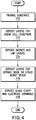
- FIG. 4 is a flow chart illustrating a method of manufacturing a multi-junction solar cell structure with a bypass diode in accordance with an embodiment of the present invention.
- the process includes providing a germanium substrate.
- the germanium substrate can be provided with a contact layer. Once the substrate is provided, the process moves to block 112.
- the process includes depositing a sequence of layers for a solar cell structure.
- the solar cell is a triple-junction solar cell, which includes bottom, middle, and top sub-cells.
- the homo-junction sub-cells can be replaced with heterojunction sub-cells.
- the process includes depositing a barrier layer and cap layer.
- a barrier layer is deposited over the window of the top sub-cell.
- a doped cap layer is deposited on the barrier layer, so that the highly-doped cap layer is spatially separated from the window of the top sub-cell.
- the barrier layer is either undoped or has a silicon density that is significantly lower than the silicon density of the cap layer.
- the barrier layer 64 is undoped, or only unintentionally doped.
- the process includes depositing a bypass diode or other active device over the cap layer.
- a stop etch layer is deposited on the cap layer
- an n-type In 0.015 GaAs layer is deposited over the stop etch layer.
- an i-type In 0.015 GaAs layer is deposited over the n-type layer, and a p-type In 0.015 GaAs layer is deposited over the i-type layer.
- the concentration of n dopant in the n-type In 0.015 GaAs layer is between 10 17 to 10 18 cm -3 .
- the concentration of p-type dopant in the p-type In 0.015 GaAs layer is between 10 17 to 10 18 cm -3 .
- the concentration of dopant for the i-type In 0.015 GaAs layer is less than 10 16 cm -3 in the particular implementation.
- a glass cover and electrode terminals can be deposited to complete formation of the solar cell.
Description
- The present disclosure relates to solar cells and the fabrication of solar cells, and more particularly multi-junction solar cells based on III - V semiconductor compounds.
- Photovoltaic cells, also called solar cells, are an important energy source that has become available in the past several years. Solar cells currently are being used in a number of commercial and consumer-oriented applications, including satellite and other space-related applications. Some solar cells have multi-junction solar cell structures that include multiple sub-cells vertically stacked one above the other on a substrate. When solar cells in an array are receiving sunlight or are illuminated, each cell is forward biased. However, if one or more of the cells are not illuminated, for example because of shadowing or damage, the shadowed cells may become reversed biased in order to carry the current generated by the illuminated cells. Such reverse biasing can degrade the cells and can ultimately render the cells inoperable. To prevent reverse biasing, a diode structure is sometimes implemented. For example,
U.S. Patent No. 6,868,414 , which is assigned to the assignee of the present application, discloses a monolithic multi-junction solar cell structure with an integrated bypass diode formed above the top sub-cell layers. The purpose of the bypass diode is to draw the current away from the shadowed or damaged cell. The bypass diode becomes forward biased when the shadowed cell becomes reverse biased. Rather than forcing current through the shadowed cell, the diode draws the current away from the shadowed cell and maintains the connection to the next cell. - Further attention is drawn to
US 2006/042684 A1 which discloses a solar cell having a multijunction solar cell structure with a bypass diode. The top cell comprises an emitter layer and a based layer with a GaAs contact on top of the emitter layer - Although fabricating the bypass diode as an integrated device can enhance its efficiency and performance, it has been discovered that fabrication of the integrated bypass diode sometimes reduces the open circuit voltage (Voc) of the top sub-cell, which can be undesirable.
- In accordance with the present invention a solar cell as set forth in claim 1 and a method of fabricating a solar cell as set forth in claim 5 are provided. Preferred embodiments of the invention are disclosed in the dependent claims.
- It is noted that the concentration of silicon in the cap layer may be, for example, in a range of about of about 1 x 10<18> cm<-3> to about 1 x 10<19> cm<-3> . In some implementations, the concentration of silicon in the cap layer is in a range of about 5 x 10<18> cm<-3> to about 6 x 10<18> cm<-3> .
- The sequence of semiconductor layers can include a multi-junction solar cell structure having a sub-cells stacked one above the other, wherein the window layer is near the top of the stack of sub-cells.
- Other features and advantages may be apparent from the following detailed description, the accompanying drawings and the claims.
-
-
FIG. 1 illustrates an example of a solar cell according to the invention. -
FIG. 2 illustrates an example of the solar cell layers according to the invention. -
FIG. 3 illustrates an example of bypass diode layers over the solar cell layers. -
FIG. 4 is a flow chart of an example of a method according to the invention. -
FIG. 1 illustrates an example of a multi-junction solar cell structure with afirst portion 12 that serves as asolar cell 10 for converting solar power to electrical power and asecond portion 14 that includes an integratedbypass diode 24 formed over the solar cell layers. Thebypass diode 24 provides reverse bias protection for thesolar cell 10. A well 16 may be formed between thesolar cell 10 and thebypass diode 24 to provide electrical separation between the active portion of the solar cell and thebypass diode 24. Thewell 16 also can provide a path for ashunt 18 to access asubstrate 36. The well subsequently may be filled with non-conductive materials such as antireflective materials. - In the illustrated example, the multi-junction
solar cell structure 22 includes abottom sub-cell 28, amiddle sub-cell 30 and atop sub-cell 32 stacked vertically over thesubstrate 36. Thesub-cells semiconductor layers 22 deposited one atop another. Above thetop cell 32 is acap layer 66, which is separated from the top cell by abarrier layer 64, which is discussed in greater detail below. -
FIG. 2 illustrates a particular implementation of the solar cell layers. In the illustrated embodiment, thesubstrate 36 is p-type germanium ("Ge"), with ametal contact pad 34. Thebottom sub-cell 28 contains a p-typeGe base layer 38, a n-typeGe emitter layer 40, and asuitable nucleation layer 42. In particular, thebase layer 38 is formed on thesubstrate 36, and the emitter andnucleation layers base layer 38. After thebottom sub-cell 28 is deposited, p-type and n-typetunneling junction layers 44 are deposited. - The
middle sub-cell 30 includes a back surface field ("BSF")layer 46, a p-typeGaAs base layer 48, an n-typeInGaP emitter layer 50, and an n-type aluminum indium phosphide2 ("AlInP2")window layer 52. Thebase layer 48 is deposited over theBSF layer 46 after the BSF layer is deposited over thetunneling junction layers 44. Thewindow layer 52 subsequently is deposited on theemitter layer 50 after the emitter layer is deposited on thebase layer 48. TheBSF layer 46 is used to reduce the recombination loss in themiddle sub-cell 30. TheBSF layer 46 drives minority carriers from a highly doped region near the back surface to minimize the effect of recombination loss. In other words, aBSF layer 46 reduces recombination loss at the backside of the solar cell and thereby reduces recombination at the base layer/BSF layer interface. - The
window layer 52 in themiddle sub-cell 30 also helps reduce the recombination loss and improves passivation of the cell surface of the underlying junctions. Additional layer(s) may be added or deleted without departing from the scope of the present invention. Before depositing thetop cell 32, p-type and n-typetunneling junction layers 54 are deposited over themiddle sub-cell 30. - The
top sub-cell 32, according to the illustrated embodiment, includes a p-type indium gallium aluminum phosphide ("InGaAlP2")BSF layer 56, a p-type GaInP2 base layer 58, an n-type GaInP2 emitter layer 60, and an n-type aluminum indium phosphide2 ("AlInP2")window layer 62. Thebase layer 58 is deposited on theBSF layer 56 after the BSF layer is deposited over thetunneling junction layers 54. Thewindow layer 62 subsequently is deposited on theemitter layer 60 after the emitter layer is deposited on thebase layer 58. In the illustrated implementation, thewindow layer 62 has a thickness of about 275 angstroms (Å). Different thicknesses may be appropriate for other implementations. - In the illustrated embodiment, a
cap layer 66 is deposited over thewindow 62 of thetop sub-cell 32 and is spatially separated from thewindow layer 62 by abarrier layer 64. The dopedcap layer 66, which serves as a contact for thetop sub-cell 32, can be, for example, a GaAs or InGaAs layer. In the illustrated implementation, thecap layer 66 is n-type In0.015GaAs. Other mole fractions can be used as well. - In the illustrated example, the
doped cap layer 66, which is employed for enhancing contact with metal materials, has a silicon concentration in the range of about 5 x 1018 cm-3 to about 6 x 1018 cm-3. More generally, the dopedcap layer 66 typically has a silicon concentration in the range of about 1 x 1018 cm-3 to about 1 x 1019 cm-3. - The
barrier layer 64 is either undoped or has a silicon density that is significantly lower than the silicon density of thecap layer 66. As used herein, a "significantly lower" silicon density means that thebarrier layer 64 layer has a silicon density at least 50% lower than the silicon density of the dopedcap layer 66. In some cases, it is preferable that thebarrier layer 64 have a silicon density that is at least two orders of magnitude lower than that of the dopedcap layer 66. Although thebarrier layer 64 preferably is not intentionally doped, small amounts of silicon may, nevertheless, be present in that layer as a contaminant. - In the illustrated implementation, the
barrier layer 64 is an undoped ("i-type"), or unintentionally-doped, GaAs or InGaAs layer. For example, thebarrier layer 64 can be undoped or unintentionally-doped In0.015GaAs. Other mole fractions can be used as well. - In the illustrated implementation, the
n+ cap layer 66 has a thickness of about 600 Å, and the undoped (or unintentionally-doped)barrier layer 64 has a thickness of about 4150 Å. Thus, thebarrier layer 64 may be several times as thick (in the illustrated example, almost seven times as thick) as the dopedcap layer 66. In any event, the higher silicon-dopedcap layer 66 is spatially separated from thewindow 62 of thetop sub-cell 32. - In the illustrated implementation, particular III - V semiconductor compounds are used in the various layers of the solar cell structure. However, the multi-junction solar cell structure can be formed by other combinations of group III to V elements listed in the periodic table, wherein the group III includes boron (B), aluminum (Al), gallium (Ga), indium (In), and thallium (Ti), the group IV includes carbon (C), silicon (Si), Ge, and tin (Sn), and the group V includes nitrogen (N), phosphorus (P), arsenic (As), antimony (Sb), and bismuth (Bi).
-
FIG. 3 illustrates a particular implementation of the additional layers that can be included over thecap layer 66 in theportion 14 for thebypass diode 24. - As shown in the example of
FIG. 3 , an etch-stop layer 68 is deposited over thecap layer 66. The etch-stop layer 68 can be, for example, n-type GaInP2. For situations in which subsequent fabrication steps take place at elevated temperatures, the etch-stop layer 68 of n-type AlGaAs may be advantageous. - After the etch-
stop layer 68 is deposited, the layers for thep-i-n bypass diode 24 are deposited, for example, epitaxially. In the illustrated embodiment, thebypass diode 24 includes a lower n-type In0.015GaAs contact layer 70, an n-type In0.015GaAs base layer 72, an i-type In0.015GaAs layer 74 layer, and a p-type In0.015GaAs emitter layer 76. The n-type base layer 72 is deposited over thecontact layer 70, the i-type layer 74 is deposited over the n-type layer 70, and the p-type layer 76 is deposited over the i-type layer 74. Afterlayer 76 is deposited, acontact pad 78 is deposited over thebypass diode 24. Thus, a p-i-n bypass diode, having p-on-n polarity, is formed over thesolar cell structure 22. In other embodiments, an n-i-p bypass diode, having n-on-p polarity, can be formed over a solar cell structure using a similar process as that described above. - In the illustrated implementation, the etch-
stop layer 68 has a thickness of about 900Ǻ. The thicknesses of the other layers in the illustrated example are as follows: contact layer 70 (1000Ǻ), base layer 72 (2000 Ǻ), intrinsic layer 74 (10000 Ǻ), emitter layer (5000 Ǻ) and contact layer 78 (500 Ǻ). - Although the foregoing discussion mentions particular examples of materials and thicknesses for various layers, other implementations may use different materials and thicknesses. Also, additional layers may be added or some layers deleted in the
bypass diode 24 without departing from the scope of the present invention. In some cases, an integrated device other than thebypass diode 24 may be formed over the solar cell layers 22. In other implementations, the solar cell structure may not include an integrated bypass diode or other device above the solar cell layers. - The inventors have discovered that the addition of the
barrier layer 64 between thedoped cap layer 66 and thewindow 62 can increase the open circuit voltage (Voc) of thetop sub-cell 32. While the theory of operation is not critical to the invention, it is believed that the addition of thebarrier layer 64 reduces diffusion of silicon from thecap layer 66 into thewindow layer 62 during growth of the bypass diode layers at elevated temperatures. The addition of thebarrier layer 64 effectively localizes the silicon in the n+ dopedlayer 66, thus preventing, or reducing, the diffusion of silicon into thewindow 62. Diffusion of silicon into thewindow 62 is undesirable because it causes out-diffusion of aluminum from thewindow 62, which in turn increases the interface minority carrier recombination and reduces the open circuit voltage (Voc) of the sub-cell. - Because the resulting open circuit voltage (Voc) of the illustrated solar cell can be higher than the open circuit voltage of a similar solar cell that does not include the undoped (or unintentionally doped)
barrier layer 64, a higher operating voltage, as well as higher power, can be obtained. That, in turn, can increase the efficiency of the solar cell. Therefore, the addition of the undoped, or unintentionally doped,barrier layer 64 can facilitate fabrication of an efficientsolar cell 20 having a multi-junctionsolar cell structure 22. -
FIG. 4 is a flow chart illustrating a method of manufacturing a multi-junction solar cell structure with a bypass diode in accordance with an embodiment of the present invention. Atblock 110, the process includes providing a germanium substrate. The germanium substrate can be provided with a contact layer. Once the substrate is provided, the process moves to block 112. - At
block 112, the process includes depositing a sequence of layers for a solar cell structure. In some embodiments, the solar cell is a triple-junction solar cell, which includes bottom, middle, and top sub-cells. The homo-junction sub-cells can be replaced with heterojunction sub-cells. After the solar cell sub-cell layers are formed, the process proceeds to block 114. - At
block 114, the process includes depositing a barrier layer and cap layer. First, a barrier layer is deposited over the window of the top sub-cell. Then, a doped cap layer is deposited on the barrier layer, so that the highly-doped cap layer is spatially separated from the window of the top sub-cell. As explained above, the barrier layer is either undoped or has a silicon density that is significantly lower than the silicon density of the cap layer. Preferably, thebarrier layer 64 is undoped, or only unintentionally doped. Once the barrier and cap layers are deposited, the process proceeds to block 116. - At
block 116, the process includes depositing a bypass diode or other active device over the cap layer. In one embodiment, after a stop etch layer is deposited on the cap layer, an n-type In0.015GaAs layer is deposited over the stop etch layer. Next, an i-type In0.015GaAs layer is deposited over the n-type layer, and a p-type In0.015GaAs layer is deposited over the i-type layer. In one embodiment, the concentration of n dopant in the n-type In0.015GaAs layer is between 1017 to 1018 cm-3. Like the n-type layer, the concentration of p-type dopant in the p-type In0.015GaAs layer is between 1017 to 1018 cm-3. In contrast, the concentration of dopant for the i-type In0.015GaAs layer is less than 1016 cm-3 in the particular implementation. - Other fabrication steps subsequently may be performed. For example, as indicated by block 118, a glass cover and electrode terminals can be deposited to complete formation of the solar cell.
- Other implementations are within the scope of the claims.
Claims (7)
- A solar cell comprising:a semiconductor substrate;a sequence of semiconductor layers disposed over the substrate, wherein the sequence of semiconductor layers includes a semiconductor window layer (62);a semiconductor silicon-containing cap layer (6) over the window layer (62), wherein the cap layer (66) is spatially separated from the window layer (62) by a semiconductor barrier layer (64) that either includes no silicon or has a silicon concentration that is at least 50% lower than the silicon density of the cap layer (66), and.wherein the window layer (62) comprises a III-V semiconductor compound containing aluminum.
- The solar cell of claim 1, wherein the concentration of silicon in the barrier layer (64) is at least two orders of magnitude less than the silicon concentration of the cap layer (66).
- The solar cell of claim 1, wherein the barrier layer (64) is at least several times thicker than the cap layer (66).
- The solar cell of claim 1, wherein each of the barrier layer (64) and cap layer (66) comprises a III-V semiconductor compound, and the barrier layer (64) has a silicon concentration that is at least two orders of magnitude less than the silicon concentration of the cap layer (62).
- A method of fabricating a solar cell comprising:depositing a sequence of semiconductor layers to form a solar cell structure over a semiconductor substrate, wherein the sequence of semiconductor layers includes a semiconductor window layer (62) comprising a III - V semiconductor compound containing aluminum.;depositing a semiconductor barrier layer (64) over the window layer (62); anddepositing a semiconductor silicon-containing cap layer (66) over the barrier layer (64),wherein the barrier layer (64) either includes no silicon or has a silicon concentration that is at least 50% lower than the silicon concentration of the cap layer (66).
- The method of claim 5, wherein the barrier layer (64) has a silicon concentration that is at least two orders of magnitude less than the silicon concentration of the cap layer (66).
- The method of claim 5, wherein the cap layer (66) has a thickness at least several times less than the barrier layer (64).
Applications Claiming Priority (1)
| Application Number | Priority Date | Filing Date | Title |
|---|---|---|---|
| US11/550,881 US7842881B2 (en) | 2006-10-19 | 2006-10-19 | Solar cell structure with localized doping in cap layer |
Publications (3)
| Publication Number | Publication Date |
|---|---|
| EP1914808A2 EP1914808A2 (en) | 2008-04-23 |
| EP1914808A3 EP1914808A3 (en) | 2013-12-25 |
| EP1914808B1 true EP1914808B1 (en) | 2018-04-04 |
Family
ID=39031008
Family Applications (1)
| Application Number | Title | Priority Date | Filing Date |
|---|---|---|---|
| EP07016452.0A Active EP1914808B1 (en) | 2006-10-19 | 2007-08-22 | Solar cell structure with localized doping of cap layer |
Country Status (4)
| Country | Link |
|---|---|
| US (1) | US7842881B2 (en) |
| EP (1) | EP1914808B1 (en) |
| JP (1) | JP4822137B2 (en) |
| CN (1) | CN101165925B (en) |
Families Citing this family (52)
| Publication number | Priority date | Publication date | Assignee | Title |
|---|---|---|---|---|
| US10170656B2 (en) | 2009-03-10 | 2019-01-01 | Solaero Technologies Corp. | Inverted metamorphic multijunction solar cell with a single metamorphic layer |
| US20100122724A1 (en) | 2008-11-14 | 2010-05-20 | Emcore Solar Power, Inc. | Four Junction Inverted Metamorphic Multijunction Solar Cell with Two Metamorphic Layers |
| US20090078310A1 (en) * | 2007-09-24 | 2009-03-26 | Emcore Corporation | Heterojunction Subcells In Inverted Metamorphic Multijunction Solar Cells |
| US20100229926A1 (en) | 2009-03-10 | 2010-09-16 | Emcore Solar Power, Inc. | Four Junction Inverted Metamorphic Multijunction Solar Cell with a Single Metamorphic Layer |
| US20090078309A1 (en) * | 2007-09-24 | 2009-03-26 | Emcore Corporation | Barrier Layers In Inverted Metamorphic Multijunction Solar Cells |
| US20100203730A1 (en) * | 2009-02-09 | 2010-08-12 | Emcore Solar Power, Inc. | Epitaxial Lift Off in Inverted Metamorphic Multijunction Solar Cells |
| US20110041898A1 (en) * | 2009-08-19 | 2011-02-24 | Emcore Solar Power, Inc. | Back Metal Layers in Inverted Metamorphic Multijunction Solar Cells |
| US8895342B2 (en) | 2007-09-24 | 2014-11-25 | Emcore Solar Power, Inc. | Heterojunction subcells in inverted metamorphic multijunction solar cells |
| US10381505B2 (en) | 2007-09-24 | 2019-08-13 | Solaero Technologies Corp. | Inverted metamorphic multijunction solar cells including metamorphic layers |
| US20100012175A1 (en) | 2008-07-16 | 2010-01-21 | Emcore Solar Power, Inc. | Ohmic n-contact formed at low temperature in inverted metamorphic multijunction solar cells |
| US20090272430A1 (en) * | 2008-04-30 | 2009-11-05 | Emcore Solar Power, Inc. | Refractive Index Matching in Inverted Metamorphic Multijunction Solar Cells |
| US20090272438A1 (en) * | 2008-05-05 | 2009-11-05 | Emcore Corporation | Strain Balanced Multiple Quantum Well Subcell In Inverted Metamorphic Multijunction Solar Cell |
| WO2009151979A2 (en) * | 2008-06-09 | 2009-12-17 | 4Power, Llc | High-efficiency solar cell structures and methods |
| US20100012174A1 (en) * | 2008-07-16 | 2010-01-21 | Emcore Corporation | High band gap contact layer in inverted metamorphic multijunction solar cells |
| US9287438B1 (en) * | 2008-07-16 | 2016-03-15 | Solaero Technologies Corp. | Method for forming ohmic N-contacts at low temperature in inverted metamorphic multijunction solar cells with contaminant isolation |
| US8263853B2 (en) | 2008-08-07 | 2012-09-11 | Emcore Solar Power, Inc. | Wafer level interconnection of inverted metamorphic multijunction solar cells |
| US8236600B2 (en) * | 2008-11-10 | 2012-08-07 | Emcore Solar Power, Inc. | Joining method for preparing an inverted metamorphic multijunction solar cell |
| US20100122764A1 (en) * | 2008-11-14 | 2010-05-20 | Emcore Solar Power, Inc. | Surrogate Substrates for Inverted Metamorphic Multijunction Solar Cells |
| US10541349B1 (en) | 2008-12-17 | 2020-01-21 | Solaero Technologies Corp. | Methods of forming inverted multijunction solar cells with distributed Bragg reflector |
| US9018521B1 (en) | 2008-12-17 | 2015-04-28 | Solaero Technologies Corp. | Inverted metamorphic multijunction solar cell with DBR layer adjacent to the top subcell |
| US7960201B2 (en) * | 2009-01-29 | 2011-06-14 | Emcore Solar Power, Inc. | String interconnection and fabrication of inverted metamorphic multijunction solar cells |
| US8778199B2 (en) | 2009-02-09 | 2014-07-15 | Emoore Solar Power, Inc. | Epitaxial lift off in inverted metamorphic multijunction solar cells |
| US20100206365A1 (en) * | 2009-02-19 | 2010-08-19 | Emcore Solar Power, Inc. | Inverted Metamorphic Multijunction Solar Cells on Low Density Carriers |
| US20100229933A1 (en) * | 2009-03-10 | 2010-09-16 | Emcore Solar Power, Inc. | Inverted Metamorphic Multijunction Solar Cells with a Supporting Coating |
| US9018519B1 (en) | 2009-03-10 | 2015-04-28 | Solaero Technologies Corp. | Inverted metamorphic multijunction solar cells having a permanent supporting substrate |
| US20100282288A1 (en) * | 2009-05-06 | 2010-11-11 | Emcore Solar Power, Inc. | Solar Cell Interconnection on a Flexible Substrate |
| US20110124146A1 (en) * | 2009-05-29 | 2011-05-26 | Pitera Arthur J | Methods of forming high-efficiency multi-junction solar cell structures |
| US20100319764A1 (en) * | 2009-06-23 | 2010-12-23 | Solar Junction Corp. | Functional Integration Of Dilute Nitrides Into High Efficiency III-V Solar Cells |
| US8263856B2 (en) * | 2009-08-07 | 2012-09-11 | Emcore Solar Power, Inc. | Inverted metamorphic multijunction solar cells with back contacts |
| US20110114163A1 (en) * | 2009-11-18 | 2011-05-19 | Solar Junction Corporation | Multijunction solar cells formed on n-doped substrates |
| US10283657B1 (en) * | 2010-01-08 | 2019-05-07 | Magnolia Optical Technologies, Inc. | Broadband photovoltaic sheets and method of constructing the same |
| US20110232730A1 (en) | 2010-03-29 | 2011-09-29 | Solar Junction Corp. | Lattice matchable alloy for solar cells |
| US8187907B1 (en) | 2010-05-07 | 2012-05-29 | Emcore Solar Power, Inc. | Solder structures for fabrication of inverted metamorphic multijunction solar cells |
| US9214580B2 (en) | 2010-10-28 | 2015-12-15 | Solar Junction Corporation | Multi-junction solar cell with dilute nitride sub-cell having graded doping |
| US8604330B1 (en) | 2010-12-06 | 2013-12-10 | 4Power, Llc | High-efficiency solar-cell arrays with integrated devices and methods for forming them |
| KR101189415B1 (en) * | 2011-01-25 | 2012-10-10 | 엘지이노텍 주식회사 | Solar cell apparatus and method of fabricating the same |
| US8962991B2 (en) | 2011-02-25 | 2015-02-24 | Solar Junction Corporation | Pseudomorphic window layer for multijunction solar cells |
| CN103168368A (en) * | 2011-04-27 | 2013-06-19 | 松下电器产业株式会社 | Method for generating power using solar battery |
| US8766087B2 (en) | 2011-05-10 | 2014-07-01 | Solar Junction Corporation | Window structure for solar cell |
| CN102254918A (en) * | 2011-07-22 | 2011-11-23 | 中国科学院苏州纳米技术与纳米仿生研究所 | Tandem solar cell and manufacturing method |
| WO2013074530A2 (en) | 2011-11-15 | 2013-05-23 | Solar Junction Corporation | High efficiency multijunction solar cells |
| US9153724B2 (en) | 2012-04-09 | 2015-10-06 | Solar Junction Corporation | Reverse heterojunctions for solar cells |
| US10153388B1 (en) | 2013-03-15 | 2018-12-11 | Solaero Technologies Corp. | Emissivity coating for space solar cell arrays |
| EP3103142B1 (en) | 2014-02-05 | 2020-08-19 | Array Photonics, Inc. | Monolithic multijunction power converter |
| US9425337B2 (en) | 2014-05-29 | 2016-08-23 | Sunpower Corporation | In-cell bypass diode |
| US20170110613A1 (en) | 2015-10-19 | 2017-04-20 | Solar Junction Corporation | High efficiency multijunction photovoltaic cells |
| CN107068787A (en) * | 2016-12-28 | 2017-08-18 | 中国电子科技集团公司第十八研究所 | The structure design and manufacture method of solar cell integrated form GaAs junction diodes |
| CN107068786A (en) * | 2016-12-28 | 2017-08-18 | 中国电子科技集团公司第十八研究所 | The structure design and manufacture method of solar cell integrated form binode diode |
| WO2019010037A1 (en) | 2017-07-06 | 2019-01-10 | Solar Junction Corporation | Hybrid mocvd/mbe epitaxial growth of high-efficiency lattice-matched multijunction solar cells |
| WO2019067553A1 (en) | 2017-09-27 | 2019-04-04 | Solar Junction Corporation | Short wavelength infrared optoelectronic devices having a dilute nitride layer |
| CN108717953A (en) * | 2018-05-25 | 2018-10-30 | 河海大学 | A kind of preparation method of P type substrate gallium antimonide thermophotovoltaic |
| WO2020185528A1 (en) | 2019-03-11 | 2020-09-17 | Array Photonics, Inc. | Short wavelength infrared optoelectronic devices having graded or stepped dilute nitride active regions |
Family Cites Families (12)
| Publication number | Priority date | Publication date | Assignee | Title |
|---|---|---|---|---|
| JP3657096B2 (en) * | 1997-10-17 | 2005-06-08 | シャープ株式会社 | GaAs solar cell |
| US5944913A (en) * | 1997-11-26 | 1999-08-31 | Sandia Corporation | High-efficiency solar cell and method for fabrication |
| US6034321A (en) * | 1998-03-24 | 2000-03-07 | Essential Research, Inc. | Dot-junction photovoltaic cells using high-absorption semiconductors |
| US6278054B1 (en) * | 1998-05-28 | 2001-08-21 | Tecstar Power Systems, Inc. | Solar cell having an integral monolithically grown bypass diode |
| JP2002517098A (en) * | 1998-05-28 | 2002-06-11 | テクスター パワー システムズ インコーポレイテッド | Solar cell with bypass diode |
| JP2005512306A (en) * | 2001-07-27 | 2005-04-28 | エムコア・コーポレイション | Solar cell device having bypass diode for reverse bias protection and method for manufacturing the same |
| US6864414B2 (en) * | 2001-10-24 | 2005-03-08 | Emcore Corporation | Apparatus and method for integral bypass diode in solar cells |
| US6680432B2 (en) * | 2001-10-24 | 2004-01-20 | Emcore Corporation | Apparatus and method for optimizing the efficiency of a bypass diode in multijunction solar cells |
| JP2003218374A (en) * | 2002-01-23 | 2003-07-31 | Sharp Corp | Group iii-v solar battery |
| US6660928B1 (en) * | 2002-04-02 | 2003-12-09 | Essential Research, Inc. | Multi-junction photovoltaic cell |
| US7071407B2 (en) | 2002-10-31 | 2006-07-04 | Emcore Corporation | Method and apparatus of multiplejunction solar cell structure with high band gap heterojunction middle cell |
| US7812249B2 (en) * | 2003-04-14 | 2010-10-12 | The Boeing Company | Multijunction photovoltaic cell grown on high-miscut-angle substrate |
-
2006
- 2006-10-19 US US11/550,881 patent/US7842881B2/en active Active
-
2007
- 2007-08-22 EP EP07016452.0A patent/EP1914808B1/en active Active
- 2007-10-15 JP JP2007267417A patent/JP4822137B2/en active Active
- 2007-10-19 CN CN2007101633849A patent/CN101165925B/en not_active Expired - Fee Related
Non-Patent Citations (1)
| Title |
|---|
| None * |
Also Published As
| Publication number | Publication date |
|---|---|
| CN101165925A (en) | 2008-04-23 |
| JP4822137B2 (en) | 2011-11-24 |
| US7842881B2 (en) | 2010-11-30 |
| US20080092943A1 (en) | 2008-04-24 |
| CN101165925B (en) | 2010-09-15 |
| EP1914808A2 (en) | 2008-04-23 |
| EP1914808A3 (en) | 2013-12-25 |
| JP2008103720A (en) | 2008-05-01 |
Similar Documents
| Publication | Publication Date | Title |
|---|---|---|
| EP1914808B1 (en) | Solar cell structure with localized doping of cap layer | |
| JP3561208B2 (en) | Two-layer passivation structure for photovoltaic cells | |
| US9691929B2 (en) | Four junction inverted metamorphic multijunction solar cell with two metamorphic layers | |
| US7592538B2 (en) | Method of fabricating a multijunction solar cell with a bypass diode having an intrinsic layer | |
| EP1440480B1 (en) | An apparatus and method for integral bypass diode in solar cells | |
| US7960201B2 (en) | String interconnection and fabrication of inverted metamorphic multijunction solar cells | |
| TWI600173B (en) | Multijunction solar cell with low band gap absorbing layer in the middle cell and method for fabricating the same | |
| US20150340530A1 (en) | Back metal layers in inverted metamorphic multijunction solar cells | |
| US7148417B1 (en) | GaP/silicon tandem solar cell with extended temperature range | |
| US20100206365A1 (en) | Inverted Metamorphic Multijunction Solar Cells on Low Density Carriers | |
| US20100122764A1 (en) | Surrogate Substrates for Inverted Metamorphic Multijunction Solar Cells | |
| US20120132250A1 (en) | Contact layout and string interconnection of inverted metamorphic multijunction solar cells | |
| US20080257405A1 (en) | Multijunction solar cell with strained-balanced quantum well middle cell | |
| US20100093127A1 (en) | Inverted Metamorphic Multijunction Solar Cell Mounted on Metallized Flexible Film | |
| US20100229926A1 (en) | Four Junction Inverted Metamorphic Multijunction Solar Cell with a Single Metamorphic Layer | |
| US20100282307A1 (en) | Multijunction Solar Cells with Group IV/III-V Hybrid Alloys for Terrestrial Applications | |
| US20150340528A1 (en) | Monolithic tandem voltage-matched multijuntion solar cells | |
| WO2003054926A2 (en) | An apparatus and method for integral bypass diode in solar cells | |
| Bertness et al. | High efficiency GaInP/GaAs tandem solar cells | |
| US9040342B2 (en) | Photovoltaic cell and manufacturing method thereof |
Legal Events
| Date | Code | Title | Description |
|---|---|---|---|
| PUAI | Public reference made under article 153(3) epc to a published international application that has entered the european phase |
Free format text: ORIGINAL CODE: 0009012 |
|
| AK | Designated contracting states |
Kind code of ref document: A2 Designated state(s): AT BE BG CH CY CZ DE DK EE ES FI FR GB GR HU IE IS IT LI LT LU LV MC MT NL PL PT RO SE SI SK TR |
|
| AX | Request for extension of the european patent |
Extension state: AL BA HR MK RS |
|
| RAP1 | Party data changed (applicant data changed or rights of an application transferred) |
Owner name: EMCORE SOLAR POWER, INC. |
|
| PUAL | Search report despatched |
Free format text: ORIGINAL CODE: 0009013 |
|
| AK | Designated contracting states |
Kind code of ref document: A3 Designated state(s): AT BE BG CH CY CZ DE DK EE ES FI FR GB GR HU IE IS IT LI LT LU LV MC MT NL PL PT RO SE SI SK TR |
|
| AX | Request for extension of the european patent |
Extension state: AL BA HR MK RS |
|
| RIC1 | Information provided on ipc code assigned before grant |
Ipc: H01L 27/142 20060101ALI20131119BHEP Ipc: H01L 31/068 20120101AFI20131119BHEP Ipc: H01L 31/0304 20060101ALI20131119BHEP |
|
| 17P | Request for examination filed |
Effective date: 20140625 |
|
| RBV | Designated contracting states (corrected) |
Designated state(s): AT BE BG CH CY CZ DE DK EE ES FI FR GB GR HU IE IS IT LI LT LU LV MC MT NL PL PT RO SE SI SK TR |
|
| RBV | Designated contracting states (corrected) |
Designated state(s): AT BE BG CH CY CZ DE DK EE ES FI FR GB GR HU IE IS IT LI LT LU LV MC MT NL PL PT RO SE SI SK TR |
|
| AKX | Designation fees paid |
Designated state(s): AT BE BG CH CY CZ DE DK EE ES FI FR GB GR HU IE IS IT LI LT LU LV MC MT NL PL PT RO SE SI SK TR |
|
| RAP1 | Party data changed (applicant data changed or rights of an application transferred) |
Owner name: SOLAERO TECHNOLOGIES CORP. |
|
| 17Q | First examination report despatched |
Effective date: 20170321 |
|
| GRAP | Despatch of communication of intention to grant a patent |
Free format text: ORIGINAL CODE: EPIDOSNIGR1 |
|
| INTG | Intention to grant announced |
Effective date: 20171024 |
|
| RIN1 | Information on inventor provided before grant (corrected) |
Inventor name: SHARPS, PAUL R. Inventor name: CORNFELD, ARTHUR Inventor name: STAN, MARK A. |
|
| GRAS | Grant fee paid |
Free format text: ORIGINAL CODE: EPIDOSNIGR3 |
|
| GRAA | (expected) grant |
Free format text: ORIGINAL CODE: 0009210 |
|
| AK | Designated contracting states |
Kind code of ref document: B1 Designated state(s): AT BE BG CH CY CZ DE DK EE ES FI FR GB GR HU IE IS IT LI LT LU LV MC MT NL PL PT RO SE SI SK TR |
|
| REG | Reference to a national code |
Ref country code: GB Ref legal event code: FG4D |
|
| REG | Reference to a national code |
Ref country code: CH Ref legal event code: EP |
|
| REG | Reference to a national code |
Ref country code: AT Ref legal event code: REF Ref document number: 986482 Country of ref document: AT Kind code of ref document: T Effective date: 20180415 |
|
| REG | Reference to a national code |
Ref country code: DE Ref legal event code: R096 Ref document number: 602007054417 Country of ref document: DE |
|
| REG | Reference to a national code |
Ref country code: IE Ref legal event code: FG4D |
|
| REG | Reference to a national code |
Ref country code: FR Ref legal event code: PLFP Year of fee payment: 12 |
|
| REG | Reference to a national code |
Ref country code: NL Ref legal event code: MP Effective date: 20180404 |
|
| REG | Reference to a national code |
Ref country code: LT Ref legal event code: MG4D |
|
| PGFP | Annual fee paid to national office [announced via postgrant information from national office to epo] |
Ref country code: BE Payment date: 20180614 Year of fee payment: 12 |
|
| PG25 | Lapsed in a contracting state [announced via postgrant information from national office to epo] |
Ref country code: NL Free format text: LAPSE BECAUSE OF FAILURE TO SUBMIT A TRANSLATION OF THE DESCRIPTION OR TO PAY THE FEE WITHIN THE PRESCRIBED TIME-LIMIT Effective date: 20180404 |
|
| PG25 | Lapsed in a contracting state [announced via postgrant information from national office to epo] |
Ref country code: FI Free format text: LAPSE BECAUSE OF FAILURE TO SUBMIT A TRANSLATION OF THE DESCRIPTION OR TO PAY THE FEE WITHIN THE PRESCRIBED TIME-LIMIT Effective date: 20180404 Ref country code: BG Free format text: LAPSE BECAUSE OF FAILURE TO SUBMIT A TRANSLATION OF THE DESCRIPTION OR TO PAY THE FEE WITHIN THE PRESCRIBED TIME-LIMIT Effective date: 20180704 Ref country code: PL Free format text: LAPSE BECAUSE OF FAILURE TO SUBMIT A TRANSLATION OF THE DESCRIPTION OR TO PAY THE FEE WITHIN THE PRESCRIBED TIME-LIMIT Effective date: 20180404 Ref country code: SE Free format text: LAPSE BECAUSE OF FAILURE TO SUBMIT A TRANSLATION OF THE DESCRIPTION OR TO PAY THE FEE WITHIN THE PRESCRIBED TIME-LIMIT Effective date: 20180404 Ref country code: ES Free format text: LAPSE BECAUSE OF FAILURE TO SUBMIT A TRANSLATION OF THE DESCRIPTION OR TO PAY THE FEE WITHIN THE PRESCRIBED TIME-LIMIT Effective date: 20180404 Ref country code: LT Free format text: LAPSE BECAUSE OF FAILURE TO SUBMIT A TRANSLATION OF THE DESCRIPTION OR TO PAY THE FEE WITHIN THE PRESCRIBED TIME-LIMIT Effective date: 20180404 |
|
| PG25 | Lapsed in a contracting state [announced via postgrant information from national office to epo] |
Ref country code: LV Free format text: LAPSE BECAUSE OF FAILURE TO SUBMIT A TRANSLATION OF THE DESCRIPTION OR TO PAY THE FEE WITHIN THE PRESCRIBED TIME-LIMIT Effective date: 20180404 Ref country code: GR Free format text: LAPSE BECAUSE OF FAILURE TO SUBMIT A TRANSLATION OF THE DESCRIPTION OR TO PAY THE FEE WITHIN THE PRESCRIBED TIME-LIMIT Effective date: 20180705 |
|
| REG | Reference to a national code |
Ref country code: AT Ref legal event code: MK05 Ref document number: 986482 Country of ref document: AT Kind code of ref document: T Effective date: 20180404 |
|
| PG25 | Lapsed in a contracting state [announced via postgrant information from national office to epo] |
Ref country code: PT Free format text: LAPSE BECAUSE OF FAILURE TO SUBMIT A TRANSLATION OF THE DESCRIPTION OR TO PAY THE FEE WITHIN THE PRESCRIBED TIME-LIMIT Effective date: 20180806 |
|
| REG | Reference to a national code |
Ref country code: DE Ref legal event code: R097 Ref document number: 602007054417 Country of ref document: DE |
|
| PG25 | Lapsed in a contracting state [announced via postgrant information from national office to epo] |
Ref country code: EE Free format text: LAPSE BECAUSE OF FAILURE TO SUBMIT A TRANSLATION OF THE DESCRIPTION OR TO PAY THE FEE WITHIN THE PRESCRIBED TIME-LIMIT Effective date: 20180404 Ref country code: CZ Free format text: LAPSE BECAUSE OF FAILURE TO SUBMIT A TRANSLATION OF THE DESCRIPTION OR TO PAY THE FEE WITHIN THE PRESCRIBED TIME-LIMIT Effective date: 20180404 Ref country code: AT Free format text: LAPSE BECAUSE OF FAILURE TO SUBMIT A TRANSLATION OF THE DESCRIPTION OR TO PAY THE FEE WITHIN THE PRESCRIBED TIME-LIMIT Effective date: 20180404 Ref country code: RO Free format text: LAPSE BECAUSE OF FAILURE TO SUBMIT A TRANSLATION OF THE DESCRIPTION OR TO PAY THE FEE WITHIN THE PRESCRIBED TIME-LIMIT Effective date: 20180404 Ref country code: DK Free format text: LAPSE BECAUSE OF FAILURE TO SUBMIT A TRANSLATION OF THE DESCRIPTION OR TO PAY THE FEE WITHIN THE PRESCRIBED TIME-LIMIT Effective date: 20180404 Ref country code: SK Free format text: LAPSE BECAUSE OF FAILURE TO SUBMIT A TRANSLATION OF THE DESCRIPTION OR TO PAY THE FEE WITHIN THE PRESCRIBED TIME-LIMIT Effective date: 20180404 |
|
| PLBE | No opposition filed within time limit |
Free format text: ORIGINAL CODE: 0009261 |
|
| STAA | Information on the status of an ep patent application or granted ep patent |
Free format text: STATUS: NO OPPOSITION FILED WITHIN TIME LIMIT |
|
| 26N | No opposition filed |
Effective date: 20190107 |
|
| PG25 | Lapsed in a contracting state [announced via postgrant information from national office to epo] |
Ref country code: MC Free format text: LAPSE BECAUSE OF FAILURE TO SUBMIT A TRANSLATION OF THE DESCRIPTION OR TO PAY THE FEE WITHIN THE PRESCRIBED TIME-LIMIT Effective date: 20180404 |
|
| REG | Reference to a national code |
Ref country code: CH Ref legal event code: PL |
|
| GBPC | Gb: european patent ceased through non-payment of renewal fee |
Effective date: 20180822 |
|
| PG25 | Lapsed in a contracting state [announced via postgrant information from national office to epo] |
Ref country code: LU Free format text: LAPSE BECAUSE OF NON-PAYMENT OF DUE FEES Effective date: 20180822 Ref country code: LI Free format text: LAPSE BECAUSE OF NON-PAYMENT OF DUE FEES Effective date: 20180831 Ref country code: CH Free format text: LAPSE BECAUSE OF NON-PAYMENT OF DUE FEES Effective date: 20180831 |
|
| PG25 | Lapsed in a contracting state [announced via postgrant information from national office to epo] |
Ref country code: SI Free format text: LAPSE BECAUSE OF FAILURE TO SUBMIT A TRANSLATION OF THE DESCRIPTION OR TO PAY THE FEE WITHIN THE PRESCRIBED TIME-LIMIT Effective date: 20180404 |
|
| PG25 | Lapsed in a contracting state [announced via postgrant information from national office to epo] |
Ref country code: IT Free format text: LAPSE BECAUSE OF NON-PAYMENT OF DUE FEES Effective date: 20180822 |
|
| PG25 | Lapsed in a contracting state [announced via postgrant information from national office to epo] |
Ref country code: GB Free format text: LAPSE BECAUSE OF NON-PAYMENT OF DUE FEES Effective date: 20180822 |
|
| PGFP | Annual fee paid to national office [announced via postgrant information from national office to epo] |
Ref country code: FR Payment date: 20190711 Year of fee payment: 13 |
|
| PG25 | Lapsed in a contracting state [announced via postgrant information from national office to epo] |
Ref country code: MT Free format text: LAPSE BECAUSE OF NON-PAYMENT OF DUE FEES Effective date: 20180822 |
|
| PG25 | Lapsed in a contracting state [announced via postgrant information from national office to epo] |
Ref country code: TR Free format text: LAPSE BECAUSE OF FAILURE TO SUBMIT A TRANSLATION OF THE DESCRIPTION OR TO PAY THE FEE WITHIN THE PRESCRIBED TIME-LIMIT Effective date: 20180404 |
|
| PG25 | Lapsed in a contracting state [announced via postgrant information from national office to epo] |
Ref country code: HU Free format text: LAPSE BECAUSE OF FAILURE TO SUBMIT A TRANSLATION OF THE DESCRIPTION OR TO PAY THE FEE WITHIN THE PRESCRIBED TIME-LIMIT; INVALID AB INITIO Effective date: 20070822 |
|
| REG | Reference to a national code |
Ref country code: BE Ref legal event code: MM Effective date: 20190831 |
|
| PG25 | Lapsed in a contracting state [announced via postgrant information from national office to epo] |
Ref country code: IE Free format text: LAPSE BECAUSE OF NON-PAYMENT OF DUE FEES Effective date: 20180822 Ref country code: CY Free format text: LAPSE BECAUSE OF FAILURE TO SUBMIT A TRANSLATION OF THE DESCRIPTION OR TO PAY THE FEE WITHIN THE PRESCRIBED TIME-LIMIT Effective date: 20180404 |
|
| PG25 | Lapsed in a contracting state [announced via postgrant information from national office to epo] |
Ref country code: IS Free format text: LAPSE BECAUSE OF FAILURE TO SUBMIT A TRANSLATION OF THE DESCRIPTION OR TO PAY THE FEE WITHIN THE PRESCRIBED TIME-LIMIT Effective date: 20180804 |
|
| PG25 | Lapsed in a contracting state [announced via postgrant information from national office to epo] |
Ref country code: BE Free format text: LAPSE BECAUSE OF NON-PAYMENT OF DUE FEES Effective date: 20190831 |
|
| PG25 | Lapsed in a contracting state [announced via postgrant information from national office to epo] |
Ref country code: FR Free format text: LAPSE BECAUSE OF NON-PAYMENT OF DUE FEES Effective date: 20200831 |
|
| PGFP | Annual fee paid to national office [announced via postgrant information from national office to epo] |
Ref country code: DE Payment date: 20230627 Year of fee payment: 17 |