EP1913437B1 - Display device and manufacturing method thereof - Google Patents
Display device and manufacturing method thereof Download PDFInfo
- Publication number
- EP1913437B1 EP1913437B1 EP06783572.8A EP06783572A EP1913437B1 EP 1913437 B1 EP1913437 B1 EP 1913437B1 EP 06783572 A EP06783572 A EP 06783572A EP 1913437 B1 EP1913437 B1 EP 1913437B1
- Authority
- EP
- European Patent Office
- Prior art keywords
- unit
- connecting unit
- main board
- display
- display device
- Prior art date
- Legal status (The legal status is an assumption and is not a legal conclusion. Google has not performed a legal analysis and makes no representation as to the accuracy of the status listed.)
- Active
Links
Images




Classifications
-
- G—PHYSICS
- G02—OPTICS
- G02F—OPTICAL DEVICES OR ARRANGEMENTS FOR THE CONTROL OF LIGHT BY MODIFICATION OF THE OPTICAL PROPERTIES OF THE MEDIA OF THE ELEMENTS INVOLVED THEREIN; NON-LINEAR OPTICS; FREQUENCY-CHANGING OF LIGHT; OPTICAL LOGIC ELEMENTS; OPTICAL ANALOGUE/DIGITAL CONVERTERS
- G02F1/00—Devices or arrangements for the control of the intensity, colour, phase, polarisation or direction of light arriving from an independent light source, e.g. switching, gating or modulating; Non-linear optics
- G02F1/01—Devices or arrangements for the control of the intensity, colour, phase, polarisation or direction of light arriving from an independent light source, e.g. switching, gating or modulating; Non-linear optics for the control of the intensity, phase, polarisation or colour
- G02F1/13—Devices or arrangements for the control of the intensity, colour, phase, polarisation or direction of light arriving from an independent light source, e.g. switching, gating or modulating; Non-linear optics for the control of the intensity, phase, polarisation or colour based on liquid crystals, e.g. single liquid crystal display cells
- G02F1/133—Constructional arrangements; Operation of liquid crystal cells; Circuit arrangements
- G02F1/1333—Constructional arrangements; Manufacturing methods
- G02F1/1345—Conductors connecting electrodes to cell terminals
-
- G—PHYSICS
- G02—OPTICS
- G02F—OPTICAL DEVICES OR ARRANGEMENTS FOR THE CONTROL OF LIGHT BY MODIFICATION OF THE OPTICAL PROPERTIES OF THE MEDIA OF THE ELEMENTS INVOLVED THEREIN; NON-LINEAR OPTICS; FREQUENCY-CHANGING OF LIGHT; OPTICAL LOGIC ELEMENTS; OPTICAL ANALOGUE/DIGITAL CONVERTERS
- G02F1/00—Devices or arrangements for the control of the intensity, colour, phase, polarisation or direction of light arriving from an independent light source, e.g. switching, gating or modulating; Non-linear optics
- G02F1/01—Devices or arrangements for the control of the intensity, colour, phase, polarisation or direction of light arriving from an independent light source, e.g. switching, gating or modulating; Non-linear optics for the control of the intensity, phase, polarisation or colour
- G02F1/13—Devices or arrangements for the control of the intensity, colour, phase, polarisation or direction of light arriving from an independent light source, e.g. switching, gating or modulating; Non-linear optics for the control of the intensity, phase, polarisation or colour based on liquid crystals, e.g. single liquid crystal display cells
- G02F1/133—Constructional arrangements; Operation of liquid crystal cells; Circuit arrangements
- G02F1/1333—Constructional arrangements; Manufacturing methods
- G02F1/1345—Conductors connecting electrodes to cell terminals
- G02F1/13452—Conductors connecting driver circuitry and terminals of panels
-
- G—PHYSICS
- G02—OPTICS
- G02F—OPTICAL DEVICES OR ARRANGEMENTS FOR THE CONTROL OF LIGHT BY MODIFICATION OF THE OPTICAL PROPERTIES OF THE MEDIA OF THE ELEMENTS INVOLVED THEREIN; NON-LINEAR OPTICS; FREQUENCY-CHANGING OF LIGHT; OPTICAL LOGIC ELEMENTS; OPTICAL ANALOGUE/DIGITAL CONVERTERS
- G02F1/00—Devices or arrangements for the control of the intensity, colour, phase, polarisation or direction of light arriving from an independent light source, e.g. switching, gating or modulating; Non-linear optics
- G02F1/01—Devices or arrangements for the control of the intensity, colour, phase, polarisation or direction of light arriving from an independent light source, e.g. switching, gating or modulating; Non-linear optics for the control of the intensity, phase, polarisation or colour
- G02F1/13—Devices or arrangements for the control of the intensity, colour, phase, polarisation or direction of light arriving from an independent light source, e.g. switching, gating or modulating; Non-linear optics for the control of the intensity, phase, polarisation or colour based on liquid crystals, e.g. single liquid crystal display cells
- G02F1/133—Constructional arrangements; Operation of liquid crystal cells; Circuit arrangements
- G02F1/1333—Constructional arrangements; Manufacturing methods
- G02F1/133342—Constructional arrangements; Manufacturing methods for double-sided displays
-
- G—PHYSICS
- G09—EDUCATION; CRYPTOGRAPHY; DISPLAY; ADVERTISING; SEALS
- G09G—ARRANGEMENTS OR CIRCUITS FOR CONTROL OF INDICATING DEVICES USING STATIC MEANS TO PRESENT VARIABLE INFORMATION
- G09G2300/00—Aspects of the constitution of display devices
- G09G2300/04—Structural and physical details of display devices
- G09G2300/0421—Structural details of the set of electrodes
- G09G2300/0426—Layout of electrodes and connections
-
- H—ELECTRICITY
- H05—ELECTRIC TECHNIQUES NOT OTHERWISE PROVIDED FOR
- H05K—PRINTED CIRCUITS; CASINGS OR CONSTRUCTIONAL DETAILS OF ELECTRIC APPARATUS; MANUFACTURE OF ASSEMBLAGES OF ELECTRICAL COMPONENTS
- H05K3/00—Apparatus or processes for manufacturing printed circuits
- H05K3/36—Assembling printed circuits with other printed circuits
- H05K3/361—Assembling flexible printed circuits with other printed circuits
Definitions
- the present invention relates to a display device and a manufacturing method thereof.
- a Braun tube display device or, cathode ray tube(CRT)
- CRT cathode ray tube
- LCDs liquid crystal display devices
- Figs. 1 and 2 show the connecting structure between display devices and a main board, according to the related art.
- Fig. 1 is a schematic view of the structure of a display device according to the related art
- Fig. 2 is a plan view showing the connected state of a display device according to JP2005-173000 .
- a display device includes a first display unit 11, a first interface unit 13, a second display unit 15, a second interface unit 17, and a main board 19.
- a display device is interconnected in the following way. First, the first display unit 11 and the first interface unit 13 are connected. Then, the second display unit 15 and the second interface unit 17 are respectively connected to each other. Subsequently, the first interface unit 13 and the main board 19 are connected, and the second interface unit 15 and the main board 19 are connected.
- the first display unit 11 and the second display unit 15 may be formed as an LCD device or an OLED device.
- the main board 19 may be formed as a rigid printed circuit board (PCB) or a flexible printed circuit board (FPCB).
- the first interface unit 13 is needed to connect the main board 19 with the first display unit 11.
- the second interface unit 17 is needed to connect the main board 19 with the second display unit 15.
- One end of the first interface unit 13 is connected to a pad unit formed on the first display unit 11, and the other end of the first interface unit 13 is connected to a pad unit formed on the main board 19.
- One end of the second interface unit 17 is connected to a pad unit formed on the second display unit 15, and the other end of the second interface unit 17 is connected to a pad unit formed on the main board 19.
- the connecting structure in the related art does not allow a direct connection between the main board 19 and the first display unit 11 and the second display unit 15.
- a pad unit, for connecting to the first display unit 11 is formed at one end of the main board 19.
- a pad unit for connecting to the second display unit 15 is formed.
- Each pad unit formed on the main board 19 is connected respectively to the first interface unit 13 and the second interface unit 17.
- the first interface unit 13 and the second interface unit 17 are additionally required, which increases cost. Also, added connecting processes for connecting the first interface unit 13 to the first display unit 11 and the second interface unit 17 to the second display unit 15 are needed, complicating manufacturing. The addition of these processes increases the number of manufacturing stages and the probability of defects.
- the present invention provides a display device and a manufacturing method thereof that simplifies the connecting of the main board to the first and the second display units, to reduce manufacturing processes and costs.
- the present invention provides a display device as defined in attached independent device claims 1 and 4, as well as a method of manufacturing the device as defined in attached independent method claims 5 and 6.
- An advantage of the display device and manufacturing method thereof according to the present invention is that they provide a simple connection between a main substrate and a first and a second display unit, to reduce manufacturing processes and costs.
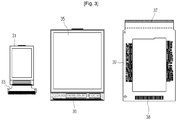
- Fig. 3 is a schematic plan view of the structure of a display device according to the present invention
- Fig. 4 is a plan view showing the connected state of a display device according to the present invention.
- a display device includes a first display unit 31, a first interface unit 33, a second display unit 35 having a second connecting unit 36, a main board 39 having a third connecting unit 37 and a fourth connecting unit 38.
- first display unit 31 and the second display unit 35 may be formed as LCDs or as as OLEDs.
- the main board 39 is formed as an FPCB.
- the first interface unit 33 may be formed as an FPCB.
- the third connecting unit 37 and the fourth connecting unit 38 are integrally formed on the main board 39.
- the second display unit 35 has the second connecting unit 36 integrally formed thereon.
- a first interface unit 33 is further included.
- the second connecting unit 36 formed on the second display unit 35 is connected directly to the third connecting unit 37 formed on the main board 39.
- the first interface unit 33 connects to the fourth connecting unit 38 formed on the main board 39, so that the main board 39 is connected to the first display unit 31.
- the main board 3 9 is formed of a multi layer of three or more layers.
- the fourth connecting unit 38 may form terminal pads on the top surface of the main board 39.
- the terminal pads of the third connecting unit 37 may be formed on the bottom surface of the main board 39, and a terminal layer located on an inner layer of the main board 39 is used to form the terminal pads.
- the fourth connecting unit 38 may form terminal pads on the upper surface of the main board 39.
- the above structured display device may be interconnected through following process.
- the first display unit 31 and the second display unit 35 having the second connecting unit 36 are provided. Then, the main board 39, on which the third connecting unit 37 and the fourth connecting unit 38 are formed, is provided.
- the first interface unit 33 is connected to the first display unit 31. Then, the first interface unit 33 is connected to the fourth connecting unit 38 formed on the main board 39, and the second connecting unit 36 of the second display unit 35 is connected directly to the third connecting unit 37 formed on the main board 39. The third connecting unit 37 is connected to the second connecting unit 36 with inserted.
- the second connecting unit 36 formed on the second display unit 35 is connected directly to the third connecting unit 37 formed on the main board 39. Accordingly, in order to connect the main board 39 and the second display unit 35, a separate interface unit is not required. Thus, the number of components and manufacturing processes can be reduced, to reduce costs and the rate of defects.
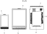
- Fig. 5 is a schematic plan view of the structure of a display device according to another embodiment of the present invention
- Fig. 6 is a plan view showing the connected state of a display device according to another embodiment of the present invention
- Fig. 7 is a plan view showing the final assembled state of a display device according to another embodiment of the present invention.
- a display device includes a first display unit 51 having a first connecting unit 52, a second display unit 55 having a second connecting unit 56, a main board 59 having a third connecting unit 57 and a fourth connecting unit 60.
- the first display unit 51 and the second display unit 55 may be formed as LCDs or OLEDs.
- the main board 59 is an FPCB.
- the third connecting unit 57 and the fourth connecting unit 60 are integrally formed on the main board 59.
- the first connecting unit 52 is integrally formed on the first display unit 51.
- the second connecting unit is integrally formed on the second display unit 55.
- the second connecting unit 56 formed on the second display unit 55 is directly connected to the third connecting unit 57 formed on the main board 59.
- the third connecting unit 57 is connected to the second connecting unit 56 with inserted.
- the first connecting unit 52 formed on the first display unit 51 is directly connected to the fourth connecting unit 60 formed on the main board 59.
- the fourth connecting unit 60 is connected to the first connecting unit 52 with inserted.
- the main board 59 is formed as a multi layer of three or more layers.
- the third connecting unit 57 may form terminal pads at a bottom surface of the main board 59
- the fourth connecting unit 60 may form terminal pads at the bottom surface of the main board 59.
- the terminal pads of the third connecting unit 57 may be formed on either surfaces(top and bottom surfaces) of the main board 59 or on the bottom surface, and use a terminal layer located at an inner layer of the main board 59 to form the terminal pads.
- the terminal pads of the fourth connecting unit 60 may be formed on the bottom surface of the main board 59 and formed using a terminal layer located at an inner layer of the main board 59.
- the above structured display device is interconnected through the following process.
- the first display unit 51 having the first connecting unit 52 and the second display unit 55 having the second connecting unit 56 are provided. Then, the main board 59 having the third connecting unit 57 and the fourth connecting unit 60 is provided.
- the first connecting unit 52 of the first display unit 51 is directly connected to the fourth connecting unit 60 formed on the main board 59
- the second connecting unit 56 of the second display unit 55 is directly connected to the third connecting unit 57 formed on the main board 59.
- the fourth connecting unit 60 is connected to the first connecting unit 52 with inserted.
- the third connecting unit 57 is connected to the second connecting unit 56 with inserted.
- the second connecting unit 56 formed on the second display unit 55 is directly connected to the third connecting unit 57 formed on the main board 59, and the first connecting unit 52 formed on the first display unit 51 is directly connected to the fourth connecting unit 60 formed on the main board 59. Accordingly, a separate interface unit is not needed to connect the main board to the first display unit 51. Also, a separate interface unit is not needed to connect the main board 59 to the second display unit 55.
- the above display device according to the present invention may be applied to a mobile communication terminal, and a variety of other electronic devices which display images on both sides thereof.
- the display device according to the present invention does not need separate interface units to connect the main board to each display unit to form a product with a lower profile.
- the display device and manufacturing method thereof according to the present invention provides simple connections between the main board and first and second display units, to reduce manufacturing processes and cost, for a high industrial applicability.
Landscapes
- Physics & Mathematics (AREA)
- Nonlinear Science (AREA)
- Mathematical Physics (AREA)
- Chemical & Material Sciences (AREA)
- Crystallography & Structural Chemistry (AREA)
- General Physics & Mathematics (AREA)
- Optics & Photonics (AREA)
- Devices For Indicating Variable Information By Combining Individual Elements (AREA)
- Electroluminescent Light Sources (AREA)
- Telephone Set Structure (AREA)
Description
- The present invention relates to a display device and a manufacturing method thereof.
- Among display devices for displaying image information on a screen, a Braun tube display device (or, cathode ray tube(CRT)) has been most popularly used up to date. However, the CRT has several disadvantages that it is bulky and heavy in comparison with its display area.
- Therefore, a thin, flat panel display device with a large display area that can be used anywhere has been developed and is gradually substituting for a cathode ray tube. Liquid crystal display devices (LCDs) are especially favored since they have a much higher resolution than other flat panel display devices and are also closer in response time to CRT display devices than other types of flat panel display devices.
- Two representative display devices used on mobile communication terminals are LCDs and organic light emitting diodes (OLEDs). There is recently a growing trend for fitting mobile communication terminals with two display devices to display images in two directions. Here, one main board is connected to the two display devices.
Figs. 1 and 2 show the connecting structure between display devices and a main board, according to the related art.Fig. 1 is a schematic view of the structure of a display device according to the related art, andFig. 2 is a plan view showing the connected state of a display device according toJP2005-173000 - A display device according to the related art includes a
first display unit 11, afirst interface unit 13, asecond display unit 15, asecond interface unit 17, and amain board 19. - In the above structure, a display device according to the related art is interconnected in the following way. First, the
first display unit 11 and thefirst interface unit 13 are connected. Then, thesecond display unit 15 and thesecond interface unit 17 are respectively connected to each other. Subsequently, thefirst interface unit 13 and themain board 19 are connected, and thesecond interface unit 15 and themain board 19 are connected. - Here, the
first display unit 11 and thesecond display unit 15 may be formed as an LCD device or an OLED device. Also, themain board 19 may be formed as a rigid printed circuit board (PCB) or a flexible printed circuit board (FPCB). - The
first interface unit 13 is needed to connect themain board 19 with thefirst display unit 11. Thesecond interface unit 17 is needed to connect themain board 19 with thesecond display unit 15. One end of thefirst interface unit 13 is connected to a pad unit formed on thefirst display unit 11, and the other end of thefirst interface unit 13 is connected to a pad unit formed on themain board 19. One end of thesecond interface unit 17 is connected to a pad unit formed on thesecond display unit 15, and the other end of thesecond interface unit 17 is connected to a pad unit formed on themain board 19. - Thus, the connecting structure in the related art does not allow a direct connection between the
main board 19 and thefirst display unit 11 and thesecond display unit 15. A pad unit, for connecting to thefirst display unit 11 is formed at one end of themain board 19. At the other end of themain board 19, a pad unit for connecting to thesecond display unit 15 is formed. Each pad unit formed on themain board 19 is connected respectively to thefirst interface unit 13 and thesecond interface unit 17. - Accordingly, in order to connect the
first display unit 11 and thesecond display unit 15 to themain board 19, thefirst interface unit 13 and thesecond interface unit 17 are additionally required, which increases cost. Also, added connecting processes for connecting thefirst interface unit 13 to thefirst display unit 11 and thesecond interface unit 17 to thesecond display unit 15 are needed, complicating manufacturing. The addition of these processes increases the number of manufacturing stages and the probability of defects. - A further prior art display device is disclosed in
US 2004/0189926 A1 . - The present invention provides a display device and a manufacturing method thereof that simplifies the connecting of the main board to the first and the second display units, to reduce manufacturing processes and costs.
- The present invention provides a display device as defined in attached independent device claims 1 and 4, as well as a method of manufacturing the device as defined in attached independent method claims 5 and 6.
- An advantage of the display device and manufacturing method thereof according to the present invention is that they provide a simple connection between a main substrate and a first and a second display unit, to reduce manufacturing processes and costs.
-
-
Fig. 1 is a schematic view of the structure of a display device according to the related art -
Fig. 2 is a plan view showing the connected state of a display device according to the related art. -
Fig. 3 is a schematic plan view of the structure of a display device according to the present invention. -
Fig. 4 is a plan view showing the connected state of a display device according to the present invention. -
Fig. 5 is a schematic plan view of the structure of a display device according to another embodiment of the present invention. -
Fig. 6 is a plan view showing the connected state of a display device according to another embodiment of the present invention. -
Fig. 7 is a plan view showing the final assembled state of a display device according to another embodiment of the present invention. - Hereinafter, embodiments of a display device and a manufacturing method thereof according to the present invention will be described in detail with reference to the accompanying drawings.
-
Fig. 3 is a schematic plan view of the structure of a display device according to the present invention, andFig. 4 is a plan view showing the connected state of a display device according to the present invention. - Referring to
Figs. 3 and4 , a display device according to the present invention includes afirst display unit 31, afirst interface unit 33, asecond display unit 35 having a second connectingunit 36, amain board 39 having a third connectingunit 37 and a fourth connectingunit 38. - Here, the
first display unit 31 and thesecond display unit 35 may be formed as LCDs or as as OLEDs. Themain board 39 is formed as an FPCB. Thefirst interface unit 33 may be formed as an FPCB. - In the display device according to the present invention, the third connecting
unit 37 and the fourth connectingunit 38 are integrally formed on themain board 39. Thesecond display unit 35 has the second connectingunit 36 integrally formed thereon. To connect thefirst display unit 31 with themain board 39 in the display device according to the present invention, afirst interface unit 33 is further included. - Here, the second connecting
unit 36 formed on thesecond display unit 35 is connected directly to the third connectingunit 37 formed on themain board 39. Thefirst interface unit 33 connects to the fourth connectingunit 38 formed on themain board 39, so that themain board 39 is connected to thefirst display unit 31. - The main board 3 9 is formed of a multi layer of three or more layers.
- The fourth connecting
unit 38 may form terminal pads on the top surface of themain board 39. - When the
main board 39 is a multi layer of three or more layers, the terminal pads of the third connectingunit 37 may be formed on the bottom surface of themain board 39, and a terminal layer located on an inner layer of themain board 39 is used to form the terminal pads. The fourth connectingunit 38 may form terminal pads on the upper surface of themain board 39. - The above structured display device may be interconnected through following process.
- First, the
first display unit 31 and thesecond display unit 35 having the second connectingunit 36 are provided. Then, themain board 39, on which the third connectingunit 37 and the fourth connectingunit 38 are formed, is provided. - Next, the
first interface unit 33 is connected to thefirst display unit 31. Then, thefirst interface unit 33 is connected to the fourth connectingunit 38 formed on themain board 39, and the second connectingunit 36 of thesecond display unit 35 is connected directly to the third connectingunit 37 formed on themain board 39. The third connectingunit 37 is connected to the second connectingunit 36 with inserted. - The second connecting
unit 36 formed on thesecond display unit 35 is connected directly to the third connectingunit 37 formed on themain board 39. Accordingly, in order to connect themain board 39 and thesecond display unit 35, a separate interface unit is not required. Thus, the number of components and manufacturing processes can be reduced, to reduce costs and the rate of defects. -
Fig. 5 is a schematic plan view of the structure of a display device according to another embodiment of the present invention,Fig. 6 is a plan view showing the connected state of a display device according to another embodiment of the present invention, andFig. 7 is a plan view showing the final assembled state of a display device according to another embodiment of the present invention. - Referring to
Figs. 5 through 7 , a display device according to the present invention includes afirst display unit 51 having a first connectingunit 52, asecond display unit 55 having a second connectingunit 56, amain board 59 having a third connectingunit 57 and a fourth connectingunit 60. - Here, the
first display unit 51 and thesecond display unit 55 may be formed as LCDs or OLEDs. Themain board 59 is an FPCB. - In the display device according to the present invention, the third connecting
unit 57 and the fourth connectingunit 60 are integrally formed on themain board 59. The first connectingunit 52 is integrally formed on thefirst display unit 51. The second connecting unit is integrally formed on thesecond display unit 55. - Here, the second connecting
unit 56 formed on thesecond display unit 55 is directly connected to the third connectingunit 57 formed on themain board 59. The third connectingunit 57 is connected to the second connectingunit 56 with inserted. The first connectingunit 52 formed on thefirst display unit 51 is directly connected to the fourth connectingunit 60 formed on themain board 59. The fourth connectingunit 60 is connected to the first connectingunit 52 with inserted. - The
main board 59 is formed as a multi layer of three or more layers. - Normally, the third connecting
unit 57 may form terminal pads at a bottom surface of themain board 59, and the fourth connectingunit 60 may form terminal pads at the bottom surface of themain board 59. - When the
main board 59 is formed as a multi layer of three layers or more, the terminal pads of the third connectingunit 57 may be formed on either surfaces(top and bottom surfaces) of themain board 59 or on the bottom surface, and use a terminal layer located at an inner layer of themain board 59 to form the terminal pads. The terminal pads of the fourth connectingunit 60 may be formed on the bottom surface of themain board 59 and formed using a terminal layer located at an inner layer of themain board 59. - The above structured display device is interconnected through the following process.
- First, the
first display unit 51 having the first connectingunit 52 and thesecond display unit 55 having the second connectingunit 56 are provided. Then, themain board 59 having the third connectingunit 57 and the fourth connectingunit 60 is provided. - Next, the first connecting
unit 52 of thefirst display unit 51 is directly connected to the fourth connectingunit 60 formed on themain board 59, and the second connectingunit 56 of thesecond display unit 55 is directly connected to the third connectingunit 57 formed on themain board 59. The fourth connectingunit 60 is connected to the first connectingunit 52 with inserted. The third connectingunit 57 is connected to the second connectingunit 56 with inserted. - In the present invention, the second connecting
unit 56 formed on thesecond display unit 55 is directly connected to the third connectingunit 57 formed on themain board 59, and the first connectingunit 52 formed on thefirst display unit 51 is directly connected to the fourth connectingunit 60 formed on themain board 59. Accordingly, a separate interface unit is not needed to connect the main board to thefirst display unit 51. Also, a separate interface unit is not needed to connect themain board 59 to thesecond display unit 55. - Therefore, the number of components and manufacturing processes are reduced, thereby reducing cost and the rate of defects.
- Additionally, the above display device according to the present invention may be applied to a mobile communication terminal, and a variety of other electronic devices which display images on both sides thereof. In these cases, the display device according to the present invention does not need separate interface units to connect the main board to each display unit to form a product with a lower profile.
- The display device and manufacturing method thereof according to the present invention provides simple connections between the main board and first and second display units, to reduce manufacturing processes and cost, for a high industrial applicability.
Claims (6)
- A display device comprising:a first display unit (31) for displaying an image;a first interface unit (33) connected to the first display unit;a second display unit (35) for displaying an image and including a second connecting unit (36) formed thereon; anda main board (39) formed of a flexible printed circuit board, FPCB, and including a third connecting unit (37) connected to the second connecting unit (36), and a fourth connecting unit (38) connected to the first interface unit (33),wherein the main board (39) is formed in a multi layer of three or more layers,wherein the third connecting unit (37) comprises a plurality of terminal pads formed on a bottom surface of the main board,wherein the plurality of terminal pads of the third connecting unit (37) are formed by a terminal layer located on an inner layer of the main board (39), and wherein the third connecting unit (37) is connected to the second connecting unit (36) by insertion into the second connecting unit (36).
- The display device according to claim 1, wherein the fourth connecting unit (38) is formed on a top surface of the main board (39).
- The display device according to claim 1, wherein the first display unit (31) and/or the second display unit (35) is an LCD (liquid crystal display device) or an OLED (organic light emitting diode).
- A display device comprising:a first display unit (51) for displaying an image and including a first connecting unit formed (52) thereon;a second display unit (55) for displaying an image and including a second connecting unit (56) formed thereon; anda main board (59) formed of a flexible printed circuit board, FPCB, and including a third connecting unit (57) connected to the second connecting unit (56), and a fourth connecting unit (60) connected to the first connecting unit (52), wherein the main board (59) is formed in a multi layer of three or more layers, wherein the third connecting unit (57) comprises a plurality of terminal pads formed on a bottom surface of the main board (59),wherein the plurality of terminal pads of the third connecting unit (57) are formed by a terminal layer located on an inner layer of the main board (59),wherein a plurality of terminal pads of the fourth connecting unit (60) are formed by a terminal layer located on an inner layer of the main board (59), wherein the third connecting unit (57) is connected to the second connecting unit (56) by insertion into the second connecting unit (56), andwherein the fourth connecting unit (60) is connected to the first connecting unit (52) by insertion into the first connecting unit (52).
- A manufacturing method of a display device, comprising:providing a first display unit (31), a first interface unit (33), and a second display unit (35) including a second connecting unit (36) formed thereon;providing a main board (39) formed of a flexible printed circuit board, FPCB, and including a third connecting unit (37) and a fourth connecting unit (38) formed thereon;connecting the first display unit (31) to the first interface unit (33);connecting the first interface unit (33) to the fourth connecting unit (38) formed on the main board (39), and connecting the second connecting unit (36) of the second display unit to the third connecting unit (37) formed on the main board (39) by inserting the third connecting unit (37) into the second connecting unit (36), wherein the main board (39) is formed in a multi layer of three or more layers, wherein the third connecting unit (37) comprises a plurality of terminal pads formed on a bottom surface of the main board (39), andwherein the plurality of terminal pads of the third connecting unit (37) are formed by a terminal layer located on an inner layer of the main board (39).
- A manufacturing method of a display device, comprising:providing a first display unit (51) including a first connecting unit (52) formed thereon, and a second display unit (55) including a second connecting unit (56) formed thereon;providing a main board (59) formed of a flexible printed circuit board, FPCB, andincluding a third connecting unit (57) and a fourth connecting unit (60) formed thereon; andconnecting the first connecting unit (52) of the first display unit (51) to the fourth connecting unit (60) formed on the main board (59) by inserting the fourth connecting unit (60) into the first connecting unit (52), and connecting the second connecting unit (56) of the second display unit (55) to the third connecting unit (57) formed on the main board (59) by inserting the third connecting unit (57) into the second connecting unit (56), wherein the main board (59) is formed in a multi layer of three or more layers, wherein the third connecting unit (57) comprises a plurality of terminal pads formed on a bottom surface of the main board (59), andwherein the plurality of terminal pads of the third connecting unit (57) are formed by a terminal layer located on an inner layer of the main board (59), andwherein a plurality of terminal pads of the fourth connecting unit (60) are formed by a terminal layer located on an inner layer of the main board (59).
Applications Claiming Priority (2)
| Application Number | Priority Date | Filing Date | Title |
|---|---|---|---|
| KR1020050073747A KR100726579B1 (en) | 2005-08-11 | 2005-08-11 | Image display device and manufacturing method thereof |
| PCT/KR2006/003150 WO2007018413A1 (en) | 2005-08-11 | 2006-08-11 | Display device and manufacturing method thereof |
Publications (3)
| Publication Number | Publication Date |
|---|---|
| EP1913437A1 EP1913437A1 (en) | 2008-04-23 |
| EP1913437A4 EP1913437A4 (en) | 2009-07-01 |
| EP1913437B1 true EP1913437B1 (en) | 2019-02-27 |
Family
ID=37727555
Family Applications (1)
| Application Number | Title | Priority Date | Filing Date |
|---|---|---|---|
| EP06783572.8A Active EP1913437B1 (en) | 2005-08-11 | 2006-08-11 | Display device and manufacturing method thereof |
Country Status (6)
| Country | Link |
|---|---|
| US (1) | US7619701B2 (en) |
| EP (1) | EP1913437B1 (en) |
| JP (1) | JP4896980B2 (en) |
| KR (1) | KR100726579B1 (en) |
| CN (1) | CN101116028B (en) |
| WO (1) | WO2007018413A1 (en) |
Citations (4)
| Publication number | Priority date | Publication date | Assignee | Title |
|---|---|---|---|---|
| JP2003295213A (en) * | 2002-03-29 | 2003-10-15 | Optrex Corp | Liquid crystal display device |
| JP2003298454A (en) * | 2002-03-29 | 2003-10-17 | Toshiba Corp | Mobile communication terminal |
| CN1591558A (en) * | 2004-03-05 | 2005-03-09 | 友达光电股份有限公司 | Dual Screen Display Module |
| JP2005173000A (en) * | 2003-12-09 | 2005-06-30 | Seiko Epson Corp | Electro-optical device and electronic apparatus |
Family Cites Families (17)
| Publication number | Priority date | Publication date | Assignee | Title |
|---|---|---|---|---|
| KR100696618B1 (en) * | 2000-01-03 | 2007-03-16 | 삼성에스디아이 주식회사 | Liquid crystal display module structure |
| US6906705B2 (en) * | 2000-10-16 | 2005-06-14 | Matsushita Electric Industrial Co., Ltd. | Electronic file with flexible display medium |
| JP2003287748A (en) * | 2002-01-22 | 2003-10-10 | Sharp Corp | Liquid crystal display |
| CN100368694C (en) * | 2002-03-19 | 2008-02-13 | 松下电器产业株式会社 | Connecting shaft and opening and closing type portable terminal device having the connecting shaft |
| JP2003302621A (en) | 2002-04-09 | 2003-10-24 | Seiko Instruments Inc | Display device |
| JP3854905B2 (en) * | 2002-07-30 | 2006-12-06 | 株式会社 日立ディスプレイズ | Liquid crystal display |
| JP3789871B2 (en) | 2002-08-23 | 2006-06-28 | 三洋電機株式会社 | Foldable electronics |
| JP4283575B2 (en) * | 2003-03-24 | 2009-06-24 | シャープ株式会社 | LCD module |
| KR100917016B1 (en) * | 2003-03-24 | 2009-09-14 | 삼성전자주식회사 | LCD Display |
| JP4357868B2 (en) * | 2003-04-25 | 2009-11-04 | シャープ株式会社 | Display device |
| JP4298400B2 (en) * | 2003-06-27 | 2009-07-15 | セイコーインスツル株式会社 | Display device |
| JP4111891B2 (en) | 2003-08-21 | 2008-07-02 | シャープ株式会社 | Portable device |
| JP4469146B2 (en) * | 2003-08-27 | 2010-05-26 | セイコーインスツル株式会社 | Display device |
| JP3976722B2 (en) | 2003-10-20 | 2007-09-19 | 埼玉日本電気株式会社 | Connection structure between functional panel and circuit board via flexible wiring board and electronic device |
| JP2005136877A (en) | 2003-10-31 | 2005-05-26 | Casio Comput Co Ltd | Arrangement structure and portable communication device |
| KR20050073649A (en) * | 2004-01-09 | 2005-07-18 | 삼성전자주식회사 | Display apparatus |
| KR20060070346A (en) * | 2004-12-20 | 2006-06-23 | 삼성전자주식회사 | Display device |
-
2005
- 2005-08-11 KR KR1020050073747A patent/KR100726579B1/en not_active Expired - Lifetime
-
2006
- 2006-08-11 JP JP2008525942A patent/JP4896980B2/en active Active
- 2006-08-11 EP EP06783572.8A patent/EP1913437B1/en active Active
- 2006-08-11 US US11/913,293 patent/US7619701B2/en active Active
- 2006-08-11 CN CN2006800041344A patent/CN101116028B/en active Active
- 2006-08-11 WO PCT/KR2006/003150 patent/WO2007018413A1/en not_active Ceased
Patent Citations (4)
| Publication number | Priority date | Publication date | Assignee | Title |
|---|---|---|---|---|
| JP2003295213A (en) * | 2002-03-29 | 2003-10-15 | Optrex Corp | Liquid crystal display device |
| JP2003298454A (en) * | 2002-03-29 | 2003-10-17 | Toshiba Corp | Mobile communication terminal |
| JP2005173000A (en) * | 2003-12-09 | 2005-06-30 | Seiko Epson Corp | Electro-optical device and electronic apparatus |
| CN1591558A (en) * | 2004-03-05 | 2005-03-09 | 友达光电股份有限公司 | Dual Screen Display Module |
Also Published As
| Publication number | Publication date |
|---|---|
| JP2009505481A (en) | 2009-02-05 |
| CN101116028A (en) | 2008-01-30 |
| KR20070019818A (en) | 2007-02-15 |
| EP1913437A1 (en) | 2008-04-23 |
| KR100726579B1 (en) | 2007-06-11 |
| JP4896980B2 (en) | 2012-03-14 |
| US20080192415A1 (en) | 2008-08-14 |
| WO2007018413A1 (en) | 2007-02-15 |
| EP1913437A4 (en) | 2009-07-01 |
| US7619701B2 (en) | 2009-11-17 |
| CN101116028B (en) | 2011-02-16 |
Similar Documents
| Publication | Publication Date | Title |
|---|---|---|
| CN110310577B (en) | Display panel and preparation method thereof | |
| US11411058B2 (en) | Flexible display device | |
| US10153337B2 (en) | Flexible display device and method for manufacturing the same | |
| US20020017859A1 (en) | Flat panel display module and method of manufacturing the same | |
| US11393891B2 (en) | Display device having reduced non-display area | |
| US20210104594A1 (en) | Display panel, preparation method thereof and display device | |
| CN108089361B (en) | Display device and method for manufacturing the same | |
| US20110086451A1 (en) | Flat panel display and method of fabricating the same | |
| CN113345927B (en) | Preparation method of under-screen camera display panel and transparent display area | |
| US12262596B2 (en) | Flexible display panel with pixel islands arranged on elastic substrate manufacturing method thereof, and electronic device | |
| US11694953B2 (en) | Circuit board and method for manufacturing the same | |
| US20190387629A1 (en) | Display panel and display | |
| US12200991B2 (en) | Display module and display apparatus | |
| JP2009180904A (en) | Display device and driver IC used therefor | |
| US20050194678A1 (en) | Bonding pad structure, display panel and bonding pad array structure using the same and manufacturing method thereof | |
| CN115207044A (en) | Display device and method for manufacturing the same | |
| US7619701B2 (en) | Display device and manufacturing method thereof | |
| JP4027139B2 (en) | Liquid crystal display | |
| US20060001820A1 (en) | Liquid crystal module | |
| US20230137784A1 (en) | Display device | |
| US8179685B2 (en) | Printed circuit board and display apparatus having the same | |
| CN211654864U (en) | Novel display module, display screen and display terminal | |
| US12170285B2 (en) | Display device and manufacturing method therefor | |
| US20240055562A1 (en) | Display device | |
| KR20260070966A (en) | Display device and driving method |
Legal Events
| Date | Code | Title | Description |
|---|---|---|---|
| PUAI | Public reference made under article 153(3) epc to a published international application that has entered the european phase |
Free format text: ORIGINAL CODE: 0009012 |
|
| 17P | Request for examination filed |
Effective date: 20070801 |
|
| AK | Designated contracting states |
Kind code of ref document: A1 Designated state(s): DE GB |
|
| DAX | Request for extension of the european patent (deleted) | ||
| RBV | Designated contracting states (corrected) |
Designated state(s): DE GB |
|
| A4 | Supplementary search report drawn up and despatched |
Effective date: 20090602 |
|
| 17Q | First examination report despatched |
Effective date: 20090722 |
|
| RAP1 | Party data changed (applicant data changed or rights of an application transferred) |
Owner name: LG DISPLAY CO., LTD. |
|
| GRAP | Despatch of communication of intention to grant a patent |
Free format text: ORIGINAL CODE: EPIDOSNIGR1 |
|
| INTG | Intention to grant announced |
Effective date: 20180927 |
|
| GRAS | Grant fee paid |
Free format text: ORIGINAL CODE: EPIDOSNIGR3 |
|
| GRAA | (expected) grant |
Free format text: ORIGINAL CODE: 0009210 |
|
| AK | Designated contracting states |
Kind code of ref document: B1 Designated state(s): DE GB |
|
| REG | Reference to a national code |
Ref country code: GB Ref legal event code: FG4D |
|
| REG | Reference to a national code |
Ref country code: DE Ref legal event code: R096 Ref document number: 602006057502 Country of ref document: DE |
|
| REG | Reference to a national code |
Ref country code: DE Ref legal event code: R097 Ref document number: 602006057502 Country of ref document: DE |
|
| PLBE | No opposition filed within time limit |
Free format text: ORIGINAL CODE: 0009261 |
|
| STAA | Information on the status of an ep patent application or granted ep patent |
Free format text: STATUS: NO OPPOSITION FILED WITHIN TIME LIMIT |
|
| 26N | No opposition filed |
Effective date: 20191128 |
|
| PGFP | Annual fee paid to national office [announced via postgrant information from national office to epo] |
Ref country code: GB Payment date: 20250624 Year of fee payment: 20 |
|
| PGFP | Annual fee paid to national office [announced via postgrant information from national office to epo] |
Ref country code: DE Payment date: 20250624 Year of fee payment: 20 |