EP1913410B1 - Method and system for debug and test using replicated logic - Google Patents
Method and system for debug and test using replicated logic Download PDFInfo
- Publication number
- EP1913410B1 EP1913410B1 EP06800744A EP06800744A EP1913410B1 EP 1913410 B1 EP1913410 B1 EP 1913410B1 EP 06800744 A EP06800744 A EP 06800744A EP 06800744 A EP06800744 A EP 06800744A EP 1913410 B1 EP1913410 B1 EP 1913410B1
- Authority
- EP
- European Patent Office
- Prior art keywords
- circuit
- machine
- trigger condition
- logic
- recorded data
- Prior art date
- Legal status (The legal status is an assumption and is not a legal conclusion. Google has not performed a legal analysis and makes no representation as to the accuracy of the status listed.)
- Active
Links
- 238000000034 method Methods 0.000 title claims abstract description 28
- 238000012360 testing method Methods 0.000 title claims abstract description 19
- 238000005516 engineering process Methods 0.000 claims description 7
- 238000012546 transfer Methods 0.000 claims description 7
- 238000013507 mapping Methods 0.000 claims description 5
- 238000004458 analytical method Methods 0.000 claims description 3
- 238000004519 manufacturing process Methods 0.000 claims 8
- 238000013461 design Methods 0.000 description 20
- 230000015654 memory Effects 0.000 description 7
- 238000012986 modification Methods 0.000 description 3
- 230000004048 modification Effects 0.000 description 3
- 230000010076 replication Effects 0.000 description 3
- 238000003491 array Methods 0.000 description 2
- 230000015572 biosynthetic process Effects 0.000 description 2
- 238000004590 computer program Methods 0.000 description 2
- 238000010586 diagram Methods 0.000 description 2
- 238000004088 simulation Methods 0.000 description 2
- 238000003786 synthesis reaction Methods 0.000 description 2
- 238000004891 communication Methods 0.000 description 1
- 238000013500 data storage Methods 0.000 description 1
- 238000011982 device technology Methods 0.000 description 1
- 238000003745 diagnosis Methods 0.000 description 1
- 238000004880 explosion Methods 0.000 description 1
- 230000006870 function Effects 0.000 description 1
- 238000012545 processing Methods 0.000 description 1
- 239000004065 semiconductor Substances 0.000 description 1
- 230000002194 synthesizing effect Effects 0.000 description 1
- 238000012795 verification Methods 0.000 description 1
Images
Classifications
-
- G—PHYSICS
- G01—MEASURING; TESTING
- G01R—MEASURING ELECTRIC VARIABLES; MEASURING MAGNETIC VARIABLES
- G01R31/00—Arrangements for testing electric properties; Arrangements for locating electric faults; Arrangements for electrical testing characterised by what is being tested not provided for elsewhere
- G01R31/28—Testing of electronic circuits, e.g. by signal tracer
- G01R31/30—Marginal testing, e.g. by varying supply voltage
- G01R31/3016—Delay or race condition test, e.g. race hazard test
-
- G—PHYSICS
- G01—MEASURING; TESTING
- G01R—MEASURING ELECTRIC VARIABLES; MEASURING MAGNETIC VARIABLES
- G01R31/00—Arrangements for testing electric properties; Arrangements for locating electric faults; Arrangements for electrical testing characterised by what is being tested not provided for elsewhere
- G01R31/28—Testing of electronic circuits, e.g. by signal tracer
- G01R31/317—Testing of digital circuits
- G01R31/31705—Debugging aspects, e.g. using test circuits for debugging, using dedicated debugging test circuits
-
- G—PHYSICS
- G01—MEASURING; TESTING
- G01R—MEASURING ELECTRIC VARIABLES; MEASURING MAGNETIC VARIABLES
- G01R31/00—Arrangements for testing electric properties; Arrangements for locating electric faults; Arrangements for electrical testing characterised by what is being tested not provided for elsewhere
- G01R31/28—Testing of electronic circuits, e.g. by signal tracer
- G01R31/317—Testing of digital circuits
- G01R31/3181—Functional testing
- G01R31/3183—Generation of test inputs, e.g. test vectors, patterns or sequences
- G01R31/318342—Generation of test inputs, e.g. test vectors, patterns or sequences by preliminary fault modelling, e.g. analysis, simulation
-
- G—PHYSICS
- G01—MEASURING; TESTING
- G01R—MEASURING ELECTRIC VARIABLES; MEASURING MAGNETIC VARIABLES
- G01R31/00—Arrangements for testing electric properties; Arrangements for locating electric faults; Arrangements for electrical testing characterised by what is being tested not provided for elsewhere
- G01R31/28—Testing of electronic circuits, e.g. by signal tracer
- G01R31/317—Testing of digital circuits
- G01R31/3181—Functional testing
- G01R31/3183—Generation of test inputs, e.g. test vectors, patterns or sequences
- G01R31/318364—Generation of test inputs, e.g. test vectors, patterns or sequences as a result of hardware simulation, e.g. in an HDL environment
-
- G—PHYSICS
- G06—COMPUTING; CALCULATING OR COUNTING
- G06F—ELECTRIC DIGITAL DATA PROCESSING
- G06F30/00—Computer-aided design [CAD]
- G06F30/30—Circuit design
- G06F30/32—Circuit design at the digital level
- G06F30/33—Design verification, e.g. functional simulation or model checking
Definitions
- Embodiments of the invention relate to the field of debugging and testing integrated circuits, and more specifically to debugging and testing integrated circuits using replicated logic.
- HDLs Hardware Description Languages
- the document US 2003/0069724 concerns techniques and systems for analysis, diagnosis and debugging fabricated hardware designs at a HDL level are described.
- the document US 2004/0030999 concerns a method and apparatus provided to debug using replicated logic.
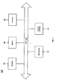
- Fig. 1 is a block diagram illustrating a suitable computing environment in which certain aspects of the illustrated invention may be practiced.
- the method described above may be implemented on a computer system 100 having components that include a processor 102, a memory 104, an Input/Output (I/O) device 106, a data storage device 112, and a network interface 110, coupled to each other via a bus 108.
- the components perform their conventional functions known in the art and provide the means for implementing the system of the invention.
- Collectively, these components represent a broad category of hardware systems, including but not limited to general purpose computer systems, mobile or wireless computing systems, and specialized packet forwarding devices.
- system 100 may be rearranged, and that certain implementations of the present invention may not require nor include all of the above components.
- additional components may be included in system 100, such as additional processors (e.g., a digital signal processor), storage devices, memories (e.g. RAM, ROM, or flash memory), and network or communication interfaces.
- the content for implementing an embodiment of a method of the invention may be provided by any machine-readable media which can store data that is accessible by system 100, as part of or in addition to memory, including but not limited to cartridges, magnetic cassettes, flash memory cards, digital video disks, random access memories (RAMs), read-only memories (ROMs), and the like.
- the system 100 is equipped to communicate with such machine-readable media in a manner well-known in the art.
- the content for implementing an embodiment of the method of the invention may be provided to the system 100 from any external device capable of storing the content and communicating the content to the system 100.
- the system 100 may be connected to a network, and the content may be stored on any device in the network.
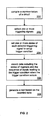
- Fig. 2 is a flow chart illustrating an embodiment of a method of the invention.
- a representation of a circuit is compiled.
- the compilation generates a first register transfer (RTL) netlist.
- the circuit is described by a text representation by writing Hardware Description Language (HDL) source code descriptions of the elements of the circuit.
- HDL Hardware Description Language
- the circuit is described by a netlist representation.
- the representation of the circuit is then input into a compiler.
- a compiler is a logic synthesis compiler, which is typically a computer program that operates on a general purpose computer system, although in some embodiments, the computer system may be a dedicated, special purpose computer system.
- a RTL netlist may be generated.
- the RTL netlist usually shows registers and other logic interconnected to show the flow of data through the circuit.
- the RTL netlist is mapped to a target architecture.
- the target architecture is typically determined by a supplier of the integrated circuit (IC). Examples of target architectures include field programmable gate arrays (FPGAs) and complex programmable logic devices from vendors such as Altera, Lucent Technologies, Advanced Micro Devices (AMD), and Lattice Semiconductor.
- FPGAs field programmable gate arrays
- ALD Advanced Micro Devices
- Lattice Semiconductor Lattice Semiconductor.
- the mapping operation converts the RTL level description of the desired circuit into the equivalent circuit implemented using building blocks of the target architecture.
- a technology specific netlist is generated. Conventional place and route software tools may then be used to create a design of circuitry in the target architecture.
- IC designers may build prototype boards using multiple ICs such as FPGAs to verify their designs. For example, after the compilation, mapping, and place and route operations, the circuit may be programmed into FPGAs to create a prototype of the design. The FPGAs can then be tested to determine any problem areas in the design.
- FPGAs field-programmable gate arrays
- the designer may further analyze the problem by selecting that portion of the circuit to replicate and by inserting trigger logic.
- One or more signals may be selected for triggering. These selected signals may be used later as trigger signals to enable a trigger condition.
- Triggering logic may then be inserted into the circuit.
- One or more controllers for the triggering logic may also be inserted into the circuit.
- a portion of the circuit may then be selected for replication and the selected portion of the circuit is replicated.
- This replication may include a replication of the logic elements, the input signals, and the output signals of the selected portion of the circuit.
- each register in the replicated portion of the circuit is connected together in a scan chain, such as a JTAG chain. This scan chain allows information from the registers, such as their states, to be scanned out during debug.
- clock signals are also replicated.
- Clock control logic is inserted to control the clock signals.
- the clock control logic allows the clock to the replicated logic block to be paused to stop the replicated logic from executing when certain conditions are present and to allow for single-stepping through the replicated logic to analyze an error.
- the designer may select a breakpoint to pause the clock to the replicated portion of the circuit when certain conditions are present. For example, the designer may choose values for the outputs or inputs that will pause the clock. This allows the designer to analyze the selected logic more carefully when certain problem conditions are present.
- Delay logic may be inserted to delay inputs into the replicated portion of the circuit.
- the length of the delay may be selected by the circuit designer.
- the delay logic allows an error observed in the selected portion of the circuit to be analyzed after the error is seen to occur since the error will reappear in the replicated portion of the circuit at a later time.
- the representation of the circuit may then be recompiled.
- the compilation generates a second RTL netlist.
- the mapping and place and route operations may be performed using the second RTL netlist to implement the circuit in a target architecture, such as a FPGA.
- a synthesis operation is performed to generate an application specific integrated circuit (ASIC) from the second RTL netlist.
- a circuit with replicated logic is produced that allows a circuit designer to analyze a problem area in the design. The designer may invoke a debugger to assist in the debugging of the circuit.
- one or more triggering signals are selected. These signals may be selected from the set of signals chosen previously, as discussed above.
- one or more states of each selected triggering signal are set to setup a triggering condition.
- data is recorded. This data includes one or more states of one or more registers and the sequence of inputs that led to the trigger condition.
- the replicated logic may be stepped clock by clock with the value of the inputs recorded at every clock. This input stream represents the sequence of inputs leading to the trigger condition that is being analyzed.
- the states of the registers in the replicated logic may also be recorded by using the scan chain implemented as described above.
- the recorded data may be converted into a format that is compatible with a software simulator.
- the software simulator is a VHDL or a Verilog simulator
- the recorded information may be converted to VHDL or Verilog, respectively.
- the formatted recorded data may then be input into the software simulator to debug logic problems in the circuit design.
- the recorded data may be input into the software simulator to verify that the circuit design remains functional when changes to the logic are made.
- a test is generated using the data recorded at 206.
- the test includes a sequence of inputs and internal states of registers that are based on the recorded sequence of inputs that led to the trigger condition and the recorded internal states of registers.
- the test may then be input into a software simulator and run when the circuit is modified to verify that the circuit remains functional. This test may be run each time the circuit is modified to ensure that the circuit is still working as expected after any modifications.
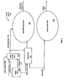
- Fig. 3 illustrates an example of a section of a circuit 300 implementing an embodiment of the invention.
- Logic block 302 is a portion of the circuit in the original IC design. Debug of the original IC design revealed a problem with logic block 302. Therefore, original logic block 302 was selected and replicated to enable further analysis of the problem.
- the original logic block 302 is replicated to produce a replicated logic block 304.
- Outputs 308 from the original logic block 302 are replicated to produce replicated outputs 310. Inputs 306 may also be replicated.
- Delay logic 312 is inserted to delay inputs 306 into replicated logic block 304.
- the delay logic includes typical circuit logic and elements, such as inverters, that cause the inputs 306 to arrive at the replicated logic block 304 later in time than the inputs 306 will arrive at the original logic block 302. In this way, an error can be analyzed after the error is seen to occur in the original logic block, since the error will appear in the replicated logic block at a later time.
- Trigger logic 330 is inserted into the circuit to enable the setup of a trigger condition that pauses the replicated portion of the circuit.
- One or more controllers may also be inserted to control the trigger logic.
- the trigger logic 330 has two outputs: breakpoint 318 and delay pause 328. Breakpoint 318 enables the clock control logic 314 to stop advancing. Delay pause 328 enables the delay logic 312 to stop advancing.
- Clock control logic 314 is inserted to control the clock signals 322 to the replicated logic block 304.
- the clock control logic 314 contains typical logic and circuit elements that allow the clock 322 to the replicated logic block 304 to be paused to stop the replicated logic from executing when certain conditions are present.
- the clock control logic 314 may also allow for single stepping through the replicated logic on a clock by clock basis to analyze an error.
- the breakpoint 318 may be set to pause the clock when certain conditions are present, such as when the trigger condition occurs.
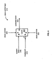
- Fig. 4 illustrates an example of the clock control logic 314 according to an embodiment of the invention.
- the system clock 316 that clocks the circuit flows through the latch 400 and acts as the clock 322 to the replicated logic block 304.
- the breakpoint 318 switches the clock 322 to a latched version of the system clock 316, which can be controlled by clock control signals 320 in order to allow the clock 322 to be paused and single-stepped on a cycle by cycle basis.
Abstract
Description
- This application is a continuation-in-part (CIP) of application no.
11/112,092, filed April 22, 2005 - Embodiments of the invention relate to the field of debugging and testing integrated circuits, and more specifically to debugging and testing integrated circuits using replicated logic.
- For the design of digital circuits, designers often employ computer aided techniques. Standard languages, such as Hardware Description Languages (HDLs), have been developed to describe digital circuits to aid in the design and simulation of complex digital circuits. As device technology continues to advance, various product design tools have been developed to adapt HDLs for use with newer devices and design styles.
- After the HDL code is written and compiled, the design of an integrated circuit (IC) or a system which includes multiple ICs must be verified to be correct. Continually advancing processing technology and the corresponding explosion in design size and complexity have led to verification problems for complex circuit designs, such as Application Specific Integrated Circuits (ASICs) that are difficult to solve using traditional simulation tools and techniques.
- As a result, some designers build prototype boards using multiple ICs such as field programmable gate arrays (FPGAs) to verify their ASIC designs. However, there are still problems with debugging the hardware design. When an error is detected during debug, designers may attempt to tap signals of interest from the circuit and use a logic analyzer to determine the cause of the error. However, this is a difficult process and is often not effective, especially in the case of intermittent errors. Errors that have already occurred are often difficult to repeat and reconstruct.
- For example the document
US 2003/0069724 concerns techniques and systems for analysis, diagnosis and debugging fabricated hardware designs at a HDL level are described. The documentUS 2004/0030999 concerns a method and apparatus provided to debug using replicated logic. - The document
US 2002/163392 concerns a method and digital circuit for synthesizing an input signal to produce an output signal. - The invention is illustrated by way of example, and not by way of limitation, in the figures of the accompanying drawings in which like reference numerals refer to similar elements.
-
Fig.1 is a block diagram illustrating a suitable computing environment in which certain aspects of the invention may be practiced. -
Fig. 2 is a flow chart illustrating an embodiment of a method of the invention. -
Fig. 3 illustrates an example of a circuit section implementing an embodiment of the invention. -
Fig. 4 illustrates an example of clock control logic according to an embodiment of the invention. - Embodiments of a system and method for debugging and testing using replicated logic are described. In the following description, numerous specific details are set forth. However, it is understood that embodiments of the invention may be practiced without these specific details. In other instances, well-known circuits, structures and techniques have not been shown in detail in order not to obscure the understanding of this description.
- Reference throughout this specification to "one embodiment" or "an embodiment" means that a particular feature, structure, or characteristic described in connection with the embodiment is included in at least one embodiment of the invention. Thus, the appearances of the phrases "in one embodiment" or "in an embodiment" in various places throughout this specification are not necessarily all referring to the same embodiment. Furthermore, the particular features, structures, or characteristics may be combined in any suitable manner in one or more embodiments.
-
Fig. 1 is a block diagram illustrating a suitable computing environment in which certain aspects of the illustrated invention may be practiced. In one embodiment, the method described above may be implemented on acomputer system 100 having components that include aprocessor 102, amemory 104, an Input/Output (I/O)device 106, adata storage device 112, and anetwork interface 110, coupled to each other via a bus 108. The components perform their conventional functions known in the art and provide the means for implementing the system of the invention. Collectively, these components represent a broad category of hardware systems, including but not limited to general purpose computer systems, mobile or wireless computing systems, and specialized packet forwarding devices. It is to be appreciated that various components ofcomputer system 100 may be rearranged, and that certain implementations of the present invention may not require nor include all of the above components. Furthermore, additional components may be included insystem 100, such as additional processors (e.g., a digital signal processor), storage devices, memories (e.g. RAM, ROM, or flash memory), and network or communication interfaces. - As will be appreciated by those skilled in the art, the content for implementing an embodiment of a method of the invention, for example, computer program instructions, may be provided by any machine-readable media which can store data that is accessible by
system 100, as part of or in addition to memory, including but not limited to cartridges, magnetic cassettes, flash memory cards, digital video disks, random access memories (RAMs), read-only memories (ROMs), and the like. In this regard, thesystem 100 is equipped to communicate with such machine-readable media in a manner well-known in the art. - It will be further appreciated by those skilled in the art that the content for implementing an embodiment of the method of the invention may be provided to the
system 100 from any external device capable of storing the content and communicating the content to thesystem 100. For example, in one embodiment, thesystem 100 may be connected to a network, and the content may be stored on any device in the network. -
Fig. 2 is a flow chart illustrating an embodiment of a method of the invention. At 200, a representation of a circuit is compiled. In one embodiment, the compilation generates a first register transfer (RTL) netlist. In one embodiment, the circuit is described by a text representation by writing Hardware Description Language (HDL) source code descriptions of the elements of the circuit. In one embodiment, the circuit is described by a netlist representation. - The representation of the circuit is then input into a compiler. One example of a compiler is a logic synthesis compiler, which is typically a computer program that operates on a general purpose computer system, although in some embodiments, the computer system may be a dedicated, special purpose computer system. After compilation, a RTL netlist may be generated. The RTL netlist usually shows registers and other logic interconnected to show the flow of data through the circuit.
- In one embodiment of the invention, the RTL netlist is mapped to a target architecture. The target architecture is typically determined by a supplier of the integrated circuit (IC). Examples of target architectures include field programmable gate arrays (FPGAs) and complex programmable logic devices from vendors such as Altera, Lucent Technologies, Advanced Micro Devices (AMD), and Lattice Semiconductor. The mapping operation converts the RTL level description of the desired circuit into the equivalent circuit implemented using building blocks of the target architecture. A technology specific netlist is generated. Conventional place and route software tools may then be used to create a design of circuitry in the target architecture.
- For debugging purposes, IC designers may build prototype boards using multiple ICs such as FPGAs to verify their designs. For example, after the compilation, mapping, and place and route operations, the circuit may be programmed into FPGAs to create a prototype of the design. The FPGAs can then be tested to determine any problem areas in the design.
- When a problem area is found in the design, the designer may further analyze the problem by selecting that portion of the circuit to replicate and by inserting trigger logic. One or more signals may be selected for triggering. These selected signals may be used later as trigger signals to enable a trigger condition.
Triggering logic may then be inserted into the circuit. One or more controllers for the triggering logic may also be inserted into the circuit. A portion of the circuit may then be selected for replication and the selected portion of the circuit is replicated. This replication may include a replication of the logic elements, the input signals, and the output signals of the selected portion of the circuit. In one embodiment, each register in the replicated portion of the circuit is connected together in a scan chain, such as a JTAG chain. This scan chain allows information from the registers, such as their states, to be scanned out during debug. - In one embodiment of the invention, clock signals are also replicated. Clock control logic is inserted to control the clock signals. The clock control logic allows the clock to the replicated logic block to be paused to stop the replicated logic from executing when certain conditions are present and to allow for single-stepping through the replicated logic to analyze an error. The designer may select a breakpoint to pause the clock to the replicated portion of the circuit when certain conditions are present. For example, the designer may choose values for the outputs or inputs that will pause the clock. This allows the designer to analyze the selected logic more carefully when certain problem conditions are present.
- Delay logic may be inserted to delay inputs into the replicated portion of the circuit. The length of the delay may be selected by the circuit designer. The delay logic allows an error observed in the selected portion of the circuit to be analyzed after the error is seen to occur since the error will reappear in the replicated portion of the circuit at a later time.
- The representation of the circuit may then be recompiled. In one embodiment, the compilation generates a second RTL netlist. Then, the mapping and place and route operations may be performed using the second RTL netlist to implement the circuit in a target architecture, such as a FPGA. In one embodiment of the invention, a synthesis operation is performed to generate an application specific integrated circuit (ASIC) from the second RTL netlist. A circuit with replicated logic is produced that allows a circuit designer to analyze a problem area in the design. The designer may invoke a debugger to assist in the debugging of the circuit.
- At 202, one or more triggering signals are selected. These signals may be selected from the set of signals chosen previously, as discussed above. At 204, one or more states of each selected triggering signal are set to setup a triggering condition. At 206, when the trigger condition occurs, data is recorded. This data includes one or more states of one or more registers and the sequence of inputs that led to the trigger condition. The replicated logic may be stepped clock by clock with the value of the inputs recorded at every clock. This input stream represents the sequence of inputs leading to the trigger condition that is being analyzed. The states of the registers in the replicated logic may also be recorded by using the scan chain implemented as described above.
- In one embodiment, the recorded data may be converted into a format that is compatible with a software simulator. For example, if the software simulator is a VHDL or a Verilog simulator, then the recorded information may be converted to VHDL or Verilog, respectively. In one embodiment, the formatted recorded data may then be input into the software simulator to debug logic problems in the circuit design. In one embodiment, the recorded data may be input into the software simulator to verify that the circuit design remains functional when changes to the logic are made.
- At 208, a test is generated using the data recorded at 206. The test includes a sequence of inputs and internal states of registers that are based on the recorded sequence of inputs that led to the trigger condition and the recorded internal states of registers. The test may then be input into a software simulator and run when the circuit is modified to verify that the circuit remains functional. This test may be run each time the circuit is modified to ensure that the circuit is still working as expected after any modifications.
-
Fig. 3 illustrates an example of a section of acircuit 300 implementing an embodiment of the invention.Logic block 302 is a portion of the circuit in the original IC design. Debug of the original IC design revealed a problem withlogic block 302. Therefore,original logic block 302 was selected and replicated to enable further analysis of the problem. Theoriginal logic block 302 is replicated to produce a replicatedlogic block 304.Outputs 308 from theoriginal logic block 302 are replicated to produce replicatedoutputs 310.Inputs 306 may also be replicated. -
Delay logic 312 is inserted to delayinputs 306 into replicatedlogic block 304. The delay logic includes typical circuit logic and elements, such as inverters, that cause theinputs 306 to arrive at the replicatedlogic block 304 later in time than theinputs 306 will arrive at theoriginal logic block 302. In this way, an error can be analyzed after the error is seen to occur in the original logic block, since the error will appear in the replicated logic block at a later time. -
Trigger logic 330 is inserted into the circuit to enable the setup of a trigger condition that pauses the replicated portion of the circuit. One or more controllers may also be inserted to control the trigger logic. Thetrigger logic 330 has two outputs:breakpoint 318 and delay pause 328.Breakpoint 318 enables theclock control logic 314 to stop advancing. Delay pause 328 enables thedelay logic 312 to stop advancing. -
Clock control logic 314 is inserted to control the clock signals 322 to the replicatedlogic block 304. Theclock control logic 314 contains typical logic and circuit elements that allow theclock 322 to the replicatedlogic block 304 to be paused to stop the replicated logic from executing when certain conditions are present. Theclock control logic 314 may also allow for single stepping through the replicated logic on a clock by clock basis to analyze an error. Thebreakpoint 318 may be set to pause the clock when certain conditions are present, such as when the trigger condition occurs. -
Fig. 4 illustrates an example of theclock control logic 314 according to an embodiment of the invention. During normal operation, thesystem clock 316 that clocks the circuit flows through thelatch 400 and acts as theclock 322 to the replicatedlogic block 304. Thebreakpoint 318 switches theclock 322 to a latched version of thesystem clock 316, which can be controlled by clock control signals 320 in order to allow theclock 322 to be paused and single-stepped on a cycle by cycle basis. - Thus, embodiments of a method and apparatus for debug and test using replicated logic have been described. The above description of illustrated embodiments of the invention, including what is described in the abstract, is not intended to be exhaustive or to limit the invention to the precise forms disclosed. While specific embodiments of, and examples for, the invention are described herein for illustrative purposes, various equivalent modifications are possible within the scope of the invention, as those skilled in the relevant art will recognize. These modifications can be made to the invention in light of the above detailed description. The terms used in the following claims should not be construed to limit the invention to the specific embodiments disclosed in the specification and the claims. Rather, the scope of the invention is to be determined by the following claims, which are to be construed in accordance with established doctrines of claim interpretation.
Claims (20)
- A method comprising:compiling a representation of a circuit, the circuit including a replicated portion and delay logic to delay inputs into the replicated portion (200), selecting one or more triggering signals (202);setting one or more states for each selected triggering signal to setup a trigger condition (204);recording data that includes one or more states of one or more registers in the replicated portion of the circuit and a sequence of inputs that led to the trigger condition when the trigger condition occurs (206); andgenerating a test based on the recorded data, the test including the recorded states of the registers and the sequence of inputs that led to the trigger condition (208).
- The method of claim 1, wherein the representation of the circuit is written in a hardware description language (HDL).
- The method of claim 1, wherein generating a test based on the recorded data comprises converting the recorded data to a format compatible with a software simulator.
- The method of claim 3, wherein converting the recorded data to a format compatible with a software simulator comprises converting the recorded data to a VHDL format to be compatible with a VHDL simulator.
- The method of claim 3, wherein converting the recorded data to a format compatible with a software simulator comprises converting the recorded data to a Verilog format to be compatible with a Verilog simulator.
- The method of claim 3, further comprising running the test on the software simulator when the circuit is modified.
- The method of claim 1, wherein compiling the representation of the circuit comprises compiling the representation of the circuit to generate a register transfer level netlist.
- The method of claim 7, further comprising mapping the register transfer level netlist to a selected technology architecture.
- The method of claim 8, further comprising performing a place and route operation to implement the circuit in the selected technology architecture.
- The method of claim 9, further comprising programming the register transfer level netlist into a programmable hardware device.
- The method of claim 10, wherein the circuit further includes trigger logic and clock control logic coupled to the replicated portion of the circuit to enable execution of the replicated portion of the circuit to be paused when the trigger condition occurs.
- The method of claim 11, further comprising running the circuit on the programmable hardware device and pausing the replicated portion of the circuit when the trigger condition occurs.
- An article of manufacture comprising:a machine accessible medium including content that when accessed by a machine causes the machine to perform operations including:compiling a representation of a circuit, the circuit including a replicated portion (304) and delay logic (312) to delay inputs into the replicated portion (304);selecting one or more triggering signals;setting one or more states for each selected triggering signal to setup a trigger condition;recording data that includes one or more states of one or more registers in the replicated portion (304) of the circuit and a sequence of inputs that led to the trigger condition when the trigger condition occurs; andgenerating a test based on the recorded data, the test including the recorded states of the registers and the sequence of inputs that led to the trigger condition.
- The article of manufacture of claim 13, wherein generating a test based on the recorded data comprises converting the recorded data to a format compatible with a software simulator.
- The article of manufacture of claim 14, wherein the machine-accessible medium further includes content that causes the machine to perform operations comprising running the test on the software simulator when the circuit is modified.
- The article of manufacture of claim 13, wherein compiling the representation of the circuit comprises compiling the representation of the circuit to generate a register transfer level netlist.
- The article of manufacture of claim 16, wherein the machine-accessible medium further includes content that causes the machine to perform operations comprising mapping the register transfer level netlist to a selected technology architecture.
- The article of manufacture of claim 17, wherein the machine-accessible medium further includes content that causes the machine to perform operations comprising performing a place and route operation to implement the circuit in the selected technology architecture.
- The article of manufacture of claim 18, wherein the machine-accessible medium further includes content that causes the machine to perform operations comprising programming the register transfer level netlist into a programmable hardware device.
- The article of manufacture of claim 19, wherein the machine-accessible medium further includes content that causes the machine to perform operations comprising recompiling the representation of the circuit after an analysis of the recorded data.
Applications Claiming Priority (2)
| Application Number | Priority Date | Filing Date | Title |
|---|---|---|---|
| US11/195,180 US7398445B2 (en) | 2002-08-09 | 2005-08-02 | Method and system for debug and test using replicated logic |
| PCT/US2006/030417 WO2007016699A2 (en) | 2005-08-02 | 2006-08-02 | Method and system for debug and test using replicated logic |
Publications (2)
| Publication Number | Publication Date |
|---|---|
| EP1913410A2 EP1913410A2 (en) | 2008-04-23 |
| EP1913410B1 true EP1913410B1 (en) | 2010-05-26 |
Family
ID=37488031
Family Applications (1)
| Application Number | Title | Priority Date | Filing Date |
|---|---|---|---|
| EP06800744A Active EP1913410B1 (en) | 2005-08-02 | 2006-08-02 | Method and system for debug and test using replicated logic |
Country Status (6)
| Country | Link |
|---|---|
| US (1) | US7398445B2 (en) |
| EP (1) | EP1913410B1 (en) |
| JP (1) | JP5039698B2 (en) |
| AT (1) | ATE469359T1 (en) |
| DE (1) | DE602006014549D1 (en) |
| WO (1) | WO2007016699A2 (en) |
Families Citing this family (11)
| Publication number | Priority date | Publication date | Assignee | Title |
|---|---|---|---|---|
| US7222315B2 (en) * | 2000-11-28 | 2007-05-22 | Synplicity, Inc. | Hardware-based HDL code coverage and design analysis |
| US7213216B2 (en) * | 2002-08-09 | 2007-05-01 | Synplicity, Inc. | Method and system for debugging using replicated logic and trigger logic |
| US6904576B2 (en) * | 2002-08-09 | 2005-06-07 | Synplicity, Inc. | Method and system for debugging using replicated logic |
| US8756557B2 (en) * | 2007-05-09 | 2014-06-17 | Synopsys, Inc. | Techniques for use with automated circuit design and simulations |
| US7908574B2 (en) * | 2007-05-09 | 2011-03-15 | Synopsys, Inc. | Techniques for use with automated circuit design and simulations |
| US7904859B2 (en) * | 2007-05-09 | 2011-03-08 | Synopsys, Inc. | Method and apparatus for determining a phase relationship between asynchronous clock signals |
| US7984400B2 (en) * | 2007-05-09 | 2011-07-19 | Synopsys, Inc. | Techniques for use with automated circuit design and simulations |
| US8397195B2 (en) * | 2010-01-22 | 2013-03-12 | Synopsys, Inc. | Method and system for packet switch based logic replication |
| US8638792B2 (en) * | 2010-01-22 | 2014-01-28 | Synopsys, Inc. | Packet switch based logic replication |
| WO2011162858A1 (en) * | 2010-06-23 | 2011-12-29 | Tabula, Inc. | Rescaling |
| US9495492B1 (en) * | 2015-01-05 | 2016-11-15 | Cadence Design Systems, Inc. | Implementing synchronous triggers for waveform capture in an FPGA prototyping system |
Family Cites Families (23)
| Publication number | Priority date | Publication date | Assignee | Title |
|---|---|---|---|---|
| EP0358365B1 (en) * | 1988-09-07 | 1998-10-21 | Texas Instruments Incorporated | Testing buffer/register |
| US5056094A (en) * | 1989-06-09 | 1991-10-08 | Texas Instruments Incorporated | Delay fault testing method and apparatus |
| US5272390A (en) * | 1991-09-23 | 1993-12-21 | Digital Equipment Corporation | Method and apparatus for clock skew reduction through absolute delay regulation |
| US5452239A (en) * | 1993-01-29 | 1995-09-19 | Quickturn Design Systems, Inc. | Method of removing gated clocks from the clock nets of a netlist for timing sensitive implementation of the netlist in a hardware emulation system |
| US5706473A (en) * | 1995-03-31 | 1998-01-06 | Synopsys, Inc. | Computer model of a finite state machine having inputs, outputs, delayed inputs and delayed outputs |
| US5761488A (en) * | 1996-06-13 | 1998-06-02 | International Business Machines Corporation | Logic translation method for increasing simulation emulation efficiency |
| JPH10177590A (en) * | 1996-12-18 | 1998-06-30 | Toshiba Corp | Device and method for debugging logic circuit model |
| US5923676A (en) * | 1996-12-20 | 1999-07-13 | Logic Vision, Inc. | Bist architecture for measurement of integrated circuit delays |
| US6286114B1 (en) * | 1997-10-27 | 2001-09-04 | Altera Corporation | Enhanced embedded logic analyzer |
| US6286128B1 (en) * | 1998-02-11 | 2001-09-04 | Monterey Design Systems, Inc. | Method for design optimization using logical and physical information |
| US6269467B1 (en) * | 1998-09-30 | 2001-07-31 | Cadence Design Systems, Inc. | Block based design methodology |
| US6438735B1 (en) * | 1999-05-17 | 2002-08-20 | Synplicity, Inc. | Methods and apparatuses for designing integrated circuits |
| US6519754B1 (en) * | 1999-05-17 | 2003-02-11 | Synplicity, Inc. | Methods and apparatuses for designing integrated circuits |
| US7065481B2 (en) * | 1999-11-30 | 2006-06-20 | Synplicity, Inc. | Method and system for debugging an electronic system using instrumentation circuitry and a logic analyzer |
| US6551227B1 (en) * | 1999-12-08 | 2003-04-22 | Heidelberger Druckmaschinen Ag | Device for seizing of flat material on a transporting surface |
| DE10030349A1 (en) | 2000-06-20 | 2002-01-10 | Kuratorium Offis E V | Method for analyzing the power loss or the energy consumption of an electrical circuit or an electrical component |
| US6516449B2 (en) * | 2001-04-02 | 2003-02-04 | Sun Microsystems, Inc. | Methodology to create integrated circuit designs by replication maintaining isomorphic input output and fault behavior |
| US6580299B2 (en) * | 2001-04-05 | 2003-06-17 | Parthus Ireland Limited | Digital circuit for, and a method of, synthesizing an input signal |
| JP2003099495A (en) * | 2001-09-25 | 2003-04-04 | Fujitsu Ltd | System and method of designing integrated circuit, and program |
| US6687882B1 (en) * | 2002-01-31 | 2004-02-03 | Synplicity, Inc. | Methods and apparatuses for non-equivalence checking of circuits with subspace |
| US6904576B2 (en) * | 2002-08-09 | 2005-06-07 | Synplicity, Inc. | Method and system for debugging using replicated logic |
| US7266489B2 (en) * | 2003-04-28 | 2007-09-04 | International Business Machines Corporation | Method, system and program product for determining a configuration of a digital design by reference to an invertible configuration database |
| US7055117B2 (en) * | 2003-12-29 | 2006-05-30 | Agere Systems, Inc. | System and method for debugging system-on-chips using single or n-cycle stepping |
-
2005
- 2005-08-02 US US11/195,180 patent/US7398445B2/en active Active
-
2006
- 2006-08-02 AT AT06800744T patent/ATE469359T1/en not_active IP Right Cessation
- 2006-08-02 JP JP2008525222A patent/JP5039698B2/en active Active
- 2006-08-02 DE DE602006014549T patent/DE602006014549D1/en active Active
- 2006-08-02 WO PCT/US2006/030417 patent/WO2007016699A2/en active Application Filing
- 2006-08-02 EP EP06800744A patent/EP1913410B1/en active Active
Also Published As
| Publication number | Publication date |
|---|---|
| WO2007016699A2 (en) | 2007-02-08 |
| US20060259834A1 (en) | 2006-11-16 |
| DE602006014549D1 (en) | 2010-07-08 |
| JP5039698B2 (en) | 2012-10-03 |
| EP1913410A2 (en) | 2008-04-23 |
| WO2007016699A3 (en) | 2007-03-29 |
| ATE469359T1 (en) | 2010-06-15 |
| US7398445B2 (en) | 2008-07-08 |
| JP2009503749A (en) | 2009-01-29 |
Similar Documents
| Publication | Publication Date | Title |
|---|---|---|
| US7962869B2 (en) | Method and system for debug and test using replicated logic | |
| US7213216B2 (en) | Method and system for debugging using replicated logic and trigger logic | |
| EP1913410B1 (en) | Method and system for debug and test using replicated logic | |
| US9064068B1 (en) | Debuggable opaque IP | |
| JP5410414B2 (en) | Circuit emulation input and delay input multiplexing | |
| Cerny et al. | SVA: the power of assertions in systemVerilog | |
| US6199031B1 (en) | HDL simulation interface for testing and verifying an ASIC model | |
| EP2165280B1 (en) | Recording of emulation states using replicated memory elements | |
| US20040122644A1 (en) | Optimized execution of software objects generated from a hardware description | |
| US7584456B1 (en) | Method and apparatus for debugging embedded systems having read only memory | |
| US7437701B1 (en) | Simulation of a programming language specification of a circuit design | |
| Sohofi et al. | Assertion-based verification for system-level designs | |
| US9235670B2 (en) | Method and an apparatus for automatic generation of verification environment for processor design and verification | |
| US6725187B1 (en) | Latch inference using dataflow analysis | |
| US7502728B1 (en) | Code coverage testing in hardware emulation | |
| Huggi et al. | Design and verification of memory elements using python | |
| Huang | On speeding up extended finite state machines using catalyst circuitry | |
| Su et al. | A Real-Time Interactive Verification System for ASIC Design | |
| Boufaied et al. | An experiment in using Esterel studio for modeling the control of mobile communication architectures | |
| Chiuchisan et al. | A Behavioral Design Approach in Verilog Hardware Description Language | |
| Bening et al. | The Bad Stuff |
Legal Events
| Date | Code | Title | Description |
|---|---|---|---|
| PUAI | Public reference made under article 153(3) epc to a published international application that has entered the european phase |
Free format text: ORIGINAL CODE: 0009012 |
|
| 17P | Request for examination filed |
Effective date: 20080229 |
|
| AK | Designated contracting states |
Kind code of ref document: A2 Designated state(s): AT BE BG CH CY CZ DE DK EE ES FI FR GB GR HU IE IS IT LI LT LU LV MC NL PL PT RO SE SI SK TR |
|
| AX | Request for extension of the european patent |
Extension state: AL BA HR MK RS |
|
| 17Q | First examination report despatched |
Effective date: 20080605 |
|
| REG | Reference to a national code |
Ref country code: HK Ref legal event code: DE Ref document number: 1116255 Country of ref document: HK |
|
| RAP1 | Party data changed (applicant data changed or rights of an application transferred) |
Owner name: SYNOPSYS, INC. |
|
| GRAP | Despatch of communication of intention to grant a patent |
Free format text: ORIGINAL CODE: EPIDOSNIGR1 |
|
| GRAS | Grant fee paid |
Free format text: ORIGINAL CODE: EPIDOSNIGR3 |
|
| GRAA | (expected) grant |
Free format text: ORIGINAL CODE: 0009210 |
|
| AK | Designated contracting states |
Kind code of ref document: B1 Designated state(s): AT BE BG CH CY CZ DE DK EE ES FI FR GB GR HU IE IS IT LI LT LU LV MC NL PL PT RO SE SI SK TR |
|
| AX | Request for extension of the european patent |
Extension state: AL BA HR MK RS |
|
| REG | Reference to a national code |
Ref country code: GB Ref legal event code: FG4D |
|
| REG | Reference to a national code |
Ref country code: CH Ref legal event code: EP |
|
| REG | Reference to a national code |
Ref country code: IE Ref legal event code: FG4D |
|
| REF | Corresponds to: |
Ref document number: 602006014549 Country of ref document: DE Date of ref document: 20100708 Kind code of ref document: P |
|
| REG | Reference to a national code |
Ref country code: NL Ref legal event code: VDEP Effective date: 20100526 |
|
| LTIE | Lt: invalidation of european patent or patent extension |
Effective date: 20100526 |
|
| PG25 | Lapsed in a contracting state [announced via postgrant information from national office to epo] |
Ref country code: SE Free format text: LAPSE BECAUSE OF FAILURE TO SUBMIT A TRANSLATION OF THE DESCRIPTION OR TO PAY THE FEE WITHIN THE PRESCRIBED TIME-LIMIT Effective date: 20100526 Ref country code: LT Free format text: LAPSE BECAUSE OF FAILURE TO SUBMIT A TRANSLATION OF THE DESCRIPTION OR TO PAY THE FEE WITHIN THE PRESCRIBED TIME-LIMIT Effective date: 20100526 |
|
| PG25 | Lapsed in a contracting state [announced via postgrant information from national office to epo] |
Ref country code: AT Free format text: LAPSE BECAUSE OF FAILURE TO SUBMIT A TRANSLATION OF THE DESCRIPTION OR TO PAY THE FEE WITHIN THE PRESCRIBED TIME-LIMIT Effective date: 20100526 Ref country code: LV Free format text: LAPSE BECAUSE OF FAILURE TO SUBMIT A TRANSLATION OF THE DESCRIPTION OR TO PAY THE FEE WITHIN THE PRESCRIBED TIME-LIMIT Effective date: 20100526 Ref country code: IS Free format text: LAPSE BECAUSE OF FAILURE TO SUBMIT A TRANSLATION OF THE DESCRIPTION OR TO PAY THE FEE WITHIN THE PRESCRIBED TIME-LIMIT Effective date: 20100926 Ref country code: FI Free format text: LAPSE BECAUSE OF FAILURE TO SUBMIT A TRANSLATION OF THE DESCRIPTION OR TO PAY THE FEE WITHIN THE PRESCRIBED TIME-LIMIT Effective date: 20100526 Ref country code: SI Free format text: LAPSE BECAUSE OF FAILURE TO SUBMIT A TRANSLATION OF THE DESCRIPTION OR TO PAY THE FEE WITHIN THE PRESCRIBED TIME-LIMIT Effective date: 20100526 |
|
| PG25 | Lapsed in a contracting state [announced via postgrant information from national office to epo] |
Ref country code: PL Free format text: LAPSE BECAUSE OF FAILURE TO SUBMIT A TRANSLATION OF THE DESCRIPTION OR TO PAY THE FEE WITHIN THE PRESCRIBED TIME-LIMIT Effective date: 20100526 Ref country code: GR Free format text: LAPSE BECAUSE OF FAILURE TO SUBMIT A TRANSLATION OF THE DESCRIPTION OR TO PAY THE FEE WITHIN THE PRESCRIBED TIME-LIMIT Effective date: 20100827 Ref country code: CY Free format text: LAPSE BECAUSE OF FAILURE TO SUBMIT A TRANSLATION OF THE DESCRIPTION OR TO PAY THE FEE WITHIN THE PRESCRIBED TIME-LIMIT Effective date: 20100526 |
|
| PG25 | Lapsed in a contracting state [announced via postgrant information from national office to epo] |
Ref country code: PT Free format text: LAPSE BECAUSE OF FAILURE TO SUBMIT A TRANSLATION OF THE DESCRIPTION OR TO PAY THE FEE WITHIN THE PRESCRIBED TIME-LIMIT Effective date: 20100927 Ref country code: NL Free format text: LAPSE BECAUSE OF FAILURE TO SUBMIT A TRANSLATION OF THE DESCRIPTION OR TO PAY THE FEE WITHIN THE PRESCRIBED TIME-LIMIT Effective date: 20100526 Ref country code: DK Free format text: LAPSE BECAUSE OF FAILURE TO SUBMIT A TRANSLATION OF THE DESCRIPTION OR TO PAY THE FEE WITHIN THE PRESCRIBED TIME-LIMIT Effective date: 20100526 Ref country code: EE Free format text: LAPSE BECAUSE OF FAILURE TO SUBMIT A TRANSLATION OF THE DESCRIPTION OR TO PAY THE FEE WITHIN THE PRESCRIBED TIME-LIMIT Effective date: 20100526 |
|
| PG25 | Lapsed in a contracting state [announced via postgrant information from national office to epo] |
Ref country code: BE Free format text: LAPSE BECAUSE OF FAILURE TO SUBMIT A TRANSLATION OF THE DESCRIPTION OR TO PAY THE FEE WITHIN THE PRESCRIBED TIME-LIMIT Effective date: 20100526 Ref country code: SK Free format text: LAPSE BECAUSE OF FAILURE TO SUBMIT A TRANSLATION OF THE DESCRIPTION OR TO PAY THE FEE WITHIN THE PRESCRIBED TIME-LIMIT Effective date: 20100526 Ref country code: RO Free format text: LAPSE BECAUSE OF FAILURE TO SUBMIT A TRANSLATION OF THE DESCRIPTION OR TO PAY THE FEE WITHIN THE PRESCRIBED TIME-LIMIT Effective date: 20100526 Ref country code: CZ Free format text: LAPSE BECAUSE OF FAILURE TO SUBMIT A TRANSLATION OF THE DESCRIPTION OR TO PAY THE FEE WITHIN THE PRESCRIBED TIME-LIMIT Effective date: 20100526 |
|
| PG25 | Lapsed in a contracting state [announced via postgrant information from national office to epo] |
Ref country code: MC Free format text: LAPSE BECAUSE OF NON-PAYMENT OF DUE FEES Effective date: 20100831 Ref country code: IT Free format text: LAPSE BECAUSE OF FAILURE TO SUBMIT A TRANSLATION OF THE DESCRIPTION OR TO PAY THE FEE WITHIN THE PRESCRIBED TIME-LIMIT Effective date: 20100526 |
|
| REG | Reference to a national code |
Ref country code: CH Ref legal event code: PL |
|
| PLBE | No opposition filed within time limit |
Free format text: ORIGINAL CODE: 0009261 |
|
| STAA | Information on the status of an ep patent application or granted ep patent |
Free format text: STATUS: NO OPPOSITION FILED WITHIN TIME LIMIT |
|
| PG25 | Lapsed in a contracting state [announced via postgrant information from national office to epo] |
Ref country code: LI Free format text: LAPSE BECAUSE OF NON-PAYMENT OF DUE FEES Effective date: 20100831 Ref country code: CH Free format text: LAPSE BECAUSE OF NON-PAYMENT OF DUE FEES Effective date: 20100831 |
|
| 26N | No opposition filed |
Effective date: 20110301 |
|
| REG | Reference to a national code |
Ref country code: DE Ref legal event code: R097 Ref document number: 602006014549 Country of ref document: DE Effective date: 20110228 |
|
| PG25 | Lapsed in a contracting state [announced via postgrant information from national office to epo] |
Ref country code: IE Free format text: LAPSE BECAUSE OF NON-PAYMENT OF DUE FEES Effective date: 20100802 |
|
| PG25 | Lapsed in a contracting state [announced via postgrant information from national office to epo] |
Ref country code: HU Free format text: LAPSE BECAUSE OF FAILURE TO SUBMIT A TRANSLATION OF THE DESCRIPTION OR TO PAY THE FEE WITHIN THE PRESCRIBED TIME-LIMIT Effective date: 20101127 Ref country code: BG Free format text: LAPSE BECAUSE OF FAILURE TO SUBMIT A TRANSLATION OF THE DESCRIPTION OR TO PAY THE FEE WITHIN THE PRESCRIBED TIME-LIMIT Effective date: 20100526 Ref country code: LU Free format text: LAPSE BECAUSE OF NON-PAYMENT OF DUE FEES Effective date: 20100802 |
|
| PG25 | Lapsed in a contracting state [announced via postgrant information from national office to epo] |
Ref country code: TR Free format text: LAPSE BECAUSE OF FAILURE TO SUBMIT A TRANSLATION OF THE DESCRIPTION OR TO PAY THE FEE WITHIN THE PRESCRIBED TIME-LIMIT Effective date: 20100526 |
|
| PG25 | Lapsed in a contracting state [announced via postgrant information from national office to epo] |
Ref country code: BG Free format text: LAPSE BECAUSE OF FAILURE TO SUBMIT A TRANSLATION OF THE DESCRIPTION OR TO PAY THE FEE WITHIN THE PRESCRIBED TIME-LIMIT Effective date: 20100826 |
|
| PG25 | Lapsed in a contracting state [announced via postgrant information from national office to epo] |
Ref country code: ES Free format text: LAPSE BECAUSE OF FAILURE TO SUBMIT A TRANSLATION OF THE DESCRIPTION OR TO PAY THE FEE WITHIN THE PRESCRIBED TIME-LIMIT Effective date: 20100906 |
|
| REG | Reference to a national code |
Ref country code: FR Ref legal event code: PLFP Year of fee payment: 11 |
|
| REG | Reference to a national code |
Ref country code: HK Ref legal event code: WD Ref document number: 1116255 Country of ref document: HK |
|
| REG | Reference to a national code |
Ref country code: FR Ref legal event code: PLFP Year of fee payment: 12 |
|
| REG | Reference to a national code |
Ref country code: FR Ref legal event code: PLFP Year of fee payment: 13 |
|
| P01 | Opt-out of the competence of the unified patent court (upc) registered |
Effective date: 20230528 |
|
| PGFP | Annual fee paid to national office [announced via postgrant information from national office to epo] |
Ref country code: GB Payment date: 20230720 Year of fee payment: 18 |
|
| PGFP | Annual fee paid to national office [announced via postgrant information from national office to epo] |
Ref country code: FR Payment date: 20230720 Year of fee payment: 18 Ref country code: DE Payment date: 20230720 Year of fee payment: 18 |