EP1911097B1 - Power semiconductor device and method of manufacturing a power semiconductor device - Google Patents
Power semiconductor device and method of manufacturing a power semiconductor device Download PDFInfo
- Publication number
- EP1911097B1 EP1911097B1 EP05789338.0A EP05789338A EP1911097B1 EP 1911097 B1 EP1911097 B1 EP 1911097B1 EP 05789338 A EP05789338 A EP 05789338A EP 1911097 B1 EP1911097 B1 EP 1911097B1
- Authority
- EP
- European Patent Office
- Prior art keywords
- face
- base
- drain
- region
- source
- Prior art date
- Legal status (The legal status is an assumption and is not a legal conclusion. Google has not performed a legal analysis and makes no representation as to the accuracy of the status listed.)
- Ceased
Links
Images


Classifications
-
- H—ELECTRICITY
- H10—SEMICONDUCTOR DEVICES; ELECTRIC SOLID-STATE DEVICES NOT OTHERWISE PROVIDED FOR
- H10D—INORGANIC ELECTRIC SEMICONDUCTOR DEVICES
- H10D30/00—Field-effect transistors [FET]
- H10D30/60—Insulated-gate field-effect transistors [IGFET]
- H10D30/64—Double-diffused metal-oxide semiconductor [DMOS] FETs
- H10D30/66—Vertical DMOS [VDMOS] FETs
-
- H—ELECTRICITY
- H10—SEMICONDUCTOR DEVICES; ELECTRIC SOLID-STATE DEVICES NOT OTHERWISE PROVIDED FOR
- H10D—INORGANIC ELECTRIC SEMICONDUCTOR DEVICES
- H10D30/00—Field-effect transistors [FET]
- H10D30/01—Manufacture or treatment
- H10D30/021—Manufacture or treatment of FETs having insulated gates [IGFET]
- H10D30/028—Manufacture or treatment of FETs having insulated gates [IGFET] of double-diffused metal oxide semiconductor [DMOS] FETs
- H10D30/0291—Manufacture or treatment of FETs having insulated gates [IGFET] of double-diffused metal oxide semiconductor [DMOS] FETs of vertical DMOS [VDMOS] FETs
-
- H—ELECTRICITY
- H10—SEMICONDUCTOR DEVICES; ELECTRIC SOLID-STATE DEVICES NOT OTHERWISE PROVIDED FOR
- H10D—INORGANIC ELECTRIC SEMICONDUCTOR DEVICES
- H10D30/00—Field-effect transistors [FET]
- H10D30/60—Insulated-gate field-effect transistors [IGFET]
- H10D30/64—Double-diffused metal-oxide semiconductor [DMOS] FETs
- H10D30/66—Vertical DMOS [VDMOS] FETs
- H10D30/665—Vertical DMOS [VDMOS] FETs having edge termination structures
-
- H—ELECTRICITY
- H10—SEMICONDUCTOR DEVICES; ELECTRIC SOLID-STATE DEVICES NOT OTHERWISE PROVIDED FOR
- H10D—INORGANIC ELECTRIC SEMICONDUCTOR DEVICES
- H10D62/00—Semiconductor bodies, or regions thereof, of devices having potential barriers
- H10D62/10—Shapes, relative sizes or dispositions of the regions of the semiconductor bodies; Shapes of the semiconductor bodies
- H10D62/13—Semiconductor regions connected to electrodes carrying current to be rectified, amplified or switched, e.g. source or drain regions
- H10D62/149—Source or drain regions of field-effect devices
- H10D62/151—Source or drain regions of field-effect devices of IGFETs
- H10D62/156—Drain regions of DMOS transistors
- H10D62/157—Impurity concentrations or distributions
-
- H—ELECTRICITY
- H10—SEMICONDUCTOR DEVICES; ELECTRIC SOLID-STATE DEVICES NOT OTHERWISE PROVIDED FOR
- H10D—INORGANIC ELECTRIC SEMICONDUCTOR DEVICES
- H10D64/00—Electrodes of devices having potential barriers
- H10D64/20—Electrodes characterised by their shapes, relative sizes or dispositions
- H10D64/27—Electrodes not carrying the current to be rectified, amplified, oscillated or switched, e.g. gates
- H10D64/311—Gate electrodes for field-effect devices
- H10D64/411—Gate electrodes for field-effect devices for FETs
- H10D64/511—Gate electrodes for field-effect devices for FETs for IGFETs
- H10D64/514—Gate electrodes for field-effect devices for FETs for IGFETs characterised by the insulating layers
- H10D64/516—Gate electrodes for field-effect devices for FETs for IGFETs characterised by the insulating layers the thicknesses being non-uniform
Definitions
- This invention relates to a power semiconductor device, especially a Metal Oxide Semiconductor Field Effect Transistor ('MOSFET'), and a method of manufacturing such a power semiconductor device.
- a power semiconductor device especially a Metal Oxide Semiconductor Field Effect Transistor ('MOSFET')
- 'MOSFET' Metal Oxide Semiconductor Field Effect Transistor
- MOSFETs Semiconductor devices such as MOSFETs have been used in power electronics applications due to their appreciable off-state voltage blocking capability and on-state current carrying capacity with low on-state resistance R DSON .
- power MOSFET devices are commonly used in many electronics fields such as portable electronics, power supplies and telecommunications and more particularly in many industrial applications relating to automotive electronics.
- an insulated gate FET (IGFET) configuration for a power MOSFET has a four-layer structure of alternating p-type and n-type doping superposed vertically in the body of the semiconductor die, that is to say superposed in a direction perpendicular to the main faces of the die.
- An example of this type of structure is the n+pn-n+ structure termed enhancement mode n-channel MOSFET.
- Source and gate electrodes are positioned in arrays of cells at one face of the device, the source electrodes contacting the source regions formed at the substrate surface in the first n+ layer and the gates being disposed over base regions in the p layer, insulated from the semiconductor material by an oxide or other insulating layer.
- One or more drain electrodes are disposed at the opposite face of the device contacting the opposite n+ layer in the substrate.
- a voltage higher than a threshold level which biases the gate positive with respect to the source, an n-type inversion layer or channel will be formed in the base regions under the gate oxide layer through the p-type layer of the cells, thus forming a connecting layer between the source and the drain regions and allowing a current to flow.
- a high cell density insulated gate IGFET configuration is preferred because of the low on-state resistance per unit area it offers.
- An example of high cell density vertical IGFET configurations is given in US Patent 6 144 067 , which describes a power MOS gated device with a strip gate poly structure to increase channel width while reducing the gate resistance.
- Other examples of IGFET are described in international patent applications WO 01/31711 and WO 01/31709 , in which a single continuous base region has an undulating structure; both devices implement a single well region made by a layout where either the gate layer substantially surrounds the base region, or the base region, which is composed of a plurality of branches, substantially surrounds the gate layer of the transistor.
- US patent 5 703 389 describes a vertical IGFET configuration having a stripe configuration wherein the stripe regions have a non linear shape that leads to an increase of the channel density.
- European patent specification EP 1 387 408 describes a low on-state resistance power semiconductor device in which each individual cell comprises a plurality of radially extending branches having source regions within base regions, at least one branch of each cell extending towards at least one branch of an adjacent cell; the base regions of the extending branches are merged together to form a single and substantially uniformly doped base region well surrounding drain islands at the surface of the semiconductor substrate.
- Other semiconductor devices having base regions common to an array of cells are described in European patent specifications EP 0 655 787 and EP 0 827 209 .
- the present invention provides a semiconductor device and a method of making a semiconductor device as described in the accompanying claims.
- EP 0335750 A2 (NEC Corporation) provides a vertical power MOSFET.
- the MOSFET addresses the problem of there being a high impurity concentration 'near the surface' in a connection region of the MOSFET.
- the solution is to provide a region of low impurity concentration near the surface of the MOSFET, above a region of high impurity concentration.
- EP 0583911 A1 (Siliconix Incorporated) provides a low threshold voltage power DMOS transistor structure.
- a lightly doped channel region is formed in a shallow layer of relatively lightly doped epitaxial silicon.
- a relatively heavily doped epitaxial layer is disposed underneath the shallow lightly doped epitaxial layer.
- a semiconductor substrate is heavily doped with impurities of a first conductivity type and is used as a collector region.
- a drift region lies above the collector region.
- An emitter region is heavily doped with impurities of a second conductivity type, and is located at an upper face of the device.
- a base region doped with impurities of the first conductivity type surrounds the emitter region.
- the semiconductor device shown in Figures 1 to 6 is a vertical insulated gate field-effect power transistor semiconductor device.
- the configuration of the device comprises an array of cells (only part of which is shown in the drawings) formed in a die of semiconductor material presenting a first face 2 and a second face 4 opposite to the first face.
- a drain electrode 6 is disposed on the second face 4 and contacts a first drain layer 8 of a first conductivity type that extends from the second face 4.
- a second superposed drain layer 10 also of the first conductivity type but having a lower dopant density than the first drain layer 8 extends from the first drain layer to the first face 2.
- Each of the basic cells comprises a source region 37 of the first conductivity type extending from the first face 2 and a base region 36 of the opposite conductivity type surrounding the source region at and below the first face.
- the base region 36 forms with the source and drain regions 37 and 36 respectively a base-source junction 12 and a base-drain junction 14, both the junctions extending to the first face so as to define respective junction perimeters 16 and 18 thereat.
- a gate electrode 32 insulated from the die by an insulating layer is disposed at the first face over at least part of the perimeters 16 and 18 of the base-source junction and the base-drain junction at the first face.
- a voltage is applied to the gate electrode 32 with the appropriate polarity (positive in the case illustrated in the drawings of an n+pnn+ device) to form a conductive channel in the base region 36 between the source region 36 and the drain layer 10.
- Figure 1 depicts in more detail, at a stage in manufacture before a base region merge operation, a top view of individual basic cells in the configuration illustrated by way of example, with the perimeters 16 and 18 of the base-source junction 12 and a base-drain junction 14 at the face 2 defining four branches arranged crosswise. This arrangement aims at having improved channel density and low on-state resistance.
- each branch 80 of the cell is seen to include a source region 37 within a base region 36 defined by the peripheries 16 and 18.
- the base region 36 also extends under the source region 37 to surround the source region in the substrate of the die.
- the base region 36 is a P-conductivity doped region in a semiconductor material that is used to provide a current channel for an IGFET.
- the current channel is controlled by the overlying insulated gate layer 32.
- An active region 39 of the less highly doped second drain layer 10, appears at the face 2 between the base regions 36 of adjacent cells of the array.
- the adjacent cells of the array are aligned and their P High Voltage ('PHV') base regions 36 are connected to each other by a merge operation of adjacent PHV regions at the ends of the branches 80 underneath the face 2 and the insulated gate electrode 32, as shown in Figure 2 and as described in more detail in our European patent specification EP 1 387 408 .
- the four branches 80 of each individual basic cell extend in straight lines and are linked to each other by four straight links 41.
- these branches may have a non-linear or undulating shape.
- the four branches may be linked by concave curving links as shown in Figure 2 , which increases the breakdown voltage capability.
- the width of the source region 37 in each branch 80 is less than the widest distance 43 between radially opposed links 41 within the cell.
- each branch 80 has a length 46 less than 10 micrometers and in this example is within a range from 2.5 to 5.0 ⁇ m.
- the spacing 47 between corresponding parallel branches 80 of adjacent cells is in a range from approximately 3.0 to 7.0 ⁇ m and in this example is between 4.0 to 5.0 ⁇ m. Smaller dimensions may be adopted, enabling increased cell density, the ultimate limit of the width 44 of each branch being defined by the photolithographic process capability.
- the base and source regions 36 and 37 are formed after insulated gate electrode 32 has been deposited onto the face 2 of the semiconductor material. After the four branches 80 are defined by etching the polysilicon of the gate electrode 32, the base region 36 is formed first followed by source region 37 by incorporating the appropriate dopants type (N-type or P-type) into the underlying semiconductor material.
- the merge operation merges the adjacent base regions 36 in the vicinity of the adjacent ends of the branches of the adjacent cells to create the contact between these well regions, by heating the die, before the source dopant is introduced into the die.
- an additional masking and implant step could be added to merge the adjacent body regions of adjacent individual cells. Further details of suitable manufacturing processes are described in our European patent specification EP 1 387 408 .
- the second drain layer 10 reaches the face 2 of the die only in drain regions 39 that are physically separated at the face 2 even though they connect electrically under the merged base regions 36.
- the periphery 18 of the base-drain junction is rounded with the base region being concave. This configuration improves breakdown voltage by reducing concentrations of electric fields.
- Figure 3 is a simplified cross-sectional view of a portion of the semiconductor device taken along line A-A of Figure 1 between the juxtaposed ends of the branches 80 of two adjacent individual cells after the merge operation.
- Figure 4 is a similar view of a portion of the semiconductor device of our European patent specification EP 1 387 408 taken along line B-B of Figure 1 between corresponding parallel branches 80 of two adjacent individual cells after the merge operation.
- a heavily doped region 38 of the same polarity as the base region is also provided having a junction in the die substrate with the source region 37 and shorted electrically to the source region by contact with the metal source electrode 40.
- the purpose of the heavily doped region 38 is to reduce the parasitic NPN or PNP bipolarity phenomenon (also called snap back effect) by ensuring that the base region will always be polarised even when evacuation of a high density of current carriers in the drain region 39 is cut off at the face 2 by switching the gate voltage to the off-state.
- the breakdown voltage is improved as well as the Unclamped Inductive Switching (UIS).
- FIG 5 illustrates graphically current flow during the on-state of the prior power switching IGFET of our European patent specification EP 1 387 408 , in which the dopant concentration of second drain does not vary substantially, in the direction laterally of the face 2, in the active drain regions 39 where they emerge at the face 2.
- each conductivity path extends generally parallel to the face 2 at 20 in its active drain region 39, and only extends perpendicular to the face 2 in the substrate to join with the drain electrode at the face 4 of the die at 22 in the central part of the active drain region 39.
- This restriction of the width of the conduction path penalises the on-state resistance R DSON but compensating it by increasing the dopant concentration of the second layer 10 would penalise the breakdown voltage.
- US patent specifications 4 376 286 and 5 075 739 describe attempts to improve the compromise but further improvement is desirable.
- This embodiment of the present invention provides an improved compromise between the on-state resistance and the breakdown voltage by enlarging the current conduction path at 24 in its active drain region 39, the current path being 'trumpet' shaped, appearing as a 'Y'-shape in the sectional view of Figure 6 .
- this is achieved by providing peripheral regions 26 in the active drain region 39 extending beside the perimeter of the base-drain junction 18, the peripheral regions being of higher dopant density than the rest of the second drain layer 10.
- intermediate regions 28 in the centre of the active drain region 39 are provided of lighter dopant density than the rest of the second drain layer 10.
- the peripheral regions 26 extend no deeper than the base regions 36.
- the higher conductivity of the peripheral regions 26 and their action in enlarging the current conduction path 24 beside the perimeter 18 of the base-drain junction enable the channel resistance R JFET to be reduced.
- any tendency of the higher dopant peripheral regions 26 to degrade the breakdown voltage of the device is more than compensated by reducing the dopant concentration in the intermediate regions 28.
- the basic cell configuration is of the kind shown in Figures 1 to 3 , with four branches 80 of each individual basic cell extending in straight lines, merged base regions 36 in the vicinity of juxtaposed ends of the source regions of adjacent cells and the periphery 18 of the base-drain junction being rounded with the base region being concave.
- the perimeters 16 and 18 of the junctions and the peripheral regions 26 are all generally ring shaped and concentric. This improves breakdown voltage by reducing electric field concentrations.
- the invention is applicable to other configurations with different numbers of branches in each cell and even to stripe and other shaped cell configurations, such as those described in our European patent specification EP 1 387 408 and other documents referred to in the introduction to this specification.
- the lightly doped region is arranged to be under a thicker 'field oxide' layer 30 where space charge extends in the off-state, which also helps to increase the breakdown voltage, whereas the insulating layer, which defines the spacing of the gate electrode 32 from the face 2, is thinner at 31 in the vicinity of said junction perimeters than in areas adjacent said intermediate regions.
- a method of making a semiconductor device with such a 'terraced' gate oxide layer and self-aligned dopant regions is described in an article by Ueda et al. in IEEE Transactions of Electronic Devices, vol. ED-31(no.4):416-20 1984 , entitled "A new vertical double diffused MOSFET - the self-aligned terraced-gate MOSFET", the teaching of which is incorporated herein by way of reference.
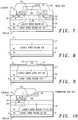
- Figures 8 and 9 illustrate steps in an example of a method of making the semiconductor device shown in Figures 6 and 7 .
- the second drain layer 10 is formed by epitaxial growth of semiconductor material on the first drain layer.
- the density of dopant in the second layer10 is reduced during the final stages of the step shown in Figure 8 of growing semiconductor material epitaxially on said first drain layer, so as to produce a layer 27 of reduced dopant density, which will remain after forming the source, base and high dopant peripheral regions therein to provide the lightly doped regions 28.
- the normal and thick oxide layers 31 and 30 are then grown on the face 2 of the die.
- the gate electrode is then formed over the oxide layers 30 and 31 by growing polysilicon and patterned by etching, using a photoresist mask.
- Other features of the gate stack such as spacers for example, are added at different stages in the process.
- the features of the gate stack are used to define automatically-aligned masking for the steps of forming the source, base and high dopant peripheral regions 37, 36 and 26.
- the high dopant peripheral regions 26 are formed by ion implant of the first conductivity type into the areas of the face 2 of the die left exposed by the oxide layers 30 and 31.
- the base regions 36 are then formed by diffusion of the opposite conductivity type and are then merged by subjecting the die to a high temperature.
- the source regions 37 are formed by diffusion of the first conductivity type and the heavily doped regions 38 are formed by diffusion of the opposite conductivity type.
- edge cells of the array that is to say the termination cells closest to the edges of the die, have a different configuration as shown in Figure 10 , notably on their outer sides facing the adjacent die edge.
- each of the edge cells comprises a source region 37 of the first conductivity type extending from the first face 2 and a base region 36 of the opposite conductivity type surrounding the source region at and below the first face.
- the base region 36 forms with the source region 37 and second drain layer 10 respectively a base-source junction 12 and a base-drain junction 14 both extending to the first face 2 so as to define respective junction perimeters 16 and 18 thereat.
- the gate electrode 32 insulated from the die, is disposed at the first face 2 extending over the base-source junction 12 and the base-drain junction 14 to form a conductive channel in the on-state of the device in the base region 36, like in the basic cells.
- the edge cell has a highly doped peripheral region 26 beside the perimeter 18 of the base-drain junction cooperating with the highly doped peripheral region 26 of the immediately adjacent basic cell in the array to form the trumpet shaped conduction path 24 and 22.
- a highly doped peripheral region 26 is also provided beside the perimeter 18 of the base-drain junction.
- the gate electrode 32 extends over and beyond at least part of the perimeters 16 and 18 of the base-source junction and the base-drain junction towards the adjacent edge of the die.
- the second drain layer 10 includes a region 27 of reduced dopant density that extends from the highly doped peripheral region 26 beyond the gate electrode right to the adjacent edge of the die.
- the thicker oxide layer 30 extends out to the edge of the die on the outer side of the edge cells. These features of the outer side of the edge cells maintain the breakdown voltage of the device that otherwise might be degraded in these outer sides.
Landscapes
- Insulated Gate Type Field-Effect Transistor (AREA)
Description
- This invention relates to a power semiconductor device, especially a Metal Oxide Semiconductor Field Effect Transistor ('MOSFET'), and a method of manufacturing such a power semiconductor device.
- Semiconductor devices such as MOSFETs have been used in power electronics applications due to their appreciable off-state voltage blocking capability and on-state current carrying capacity with low on-state resistance RDSON. In terms of industrial applications, power MOSFET devices are commonly used in many electronics fields such as portable electronics, power supplies and telecommunications and more particularly in many industrial applications relating to automotive electronics.
- Conventionally, an insulated gate FET (IGFET) configuration for a power MOSFET has a four-layer structure of alternating p-type and n-type doping superposed vertically in the body of the semiconductor die, that is to say superposed in a direction perpendicular to the main faces of the die. An example of this type of structure is the n+pn-n+ structure termed enhancement mode n-channel MOSFET. Source and gate electrodes are positioned in arrays of cells at one face of the device, the source electrodes contacting the source regions formed at the substrate surface in the first n+ layer and the gates being disposed over base regions in the p layer, insulated from the semiconductor material by an oxide or other insulating layer. One or more drain electrodes are disposed at the opposite face of the device contacting the opposite n+ layer in the substrate. By applying a voltage higher than a threshold level, which biases the gate positive with respect to the source, an n-type inversion layer or channel will be formed in the base regions under the gate oxide layer through the p-type layer of the cells, thus forming a connecting layer between the source and the drain regions and allowing a current to flow. Once the device is turned on, the relation between the current and the source-drain voltage is nearly linear which means that the device then behaves like a resistance. The on-state resistance RDSON should be as low as possible.
- A high cell density insulated gate IGFET configuration is preferred because of the low on-state resistance per unit area it offers. An example of high cell density vertical IGFET configurations is given in
US , which describes a power MOS gated device with a strip gate poly structure to increase channel width while reducing the gate resistance. Other examples of IGFET are described in international patent applicationsPatent 6 144 067WO 01/31711 WO 01/31709 US patent 5 703 389 describes a vertical IGFET configuration having a stripe configuration wherein the stripe regions have a non linear shape that leads to an increase of the channel density. - European patent specification
EP 1 387 408 describes a low on-state resistance power semiconductor device in which each individual cell comprises a plurality of radially extending branches having source regions within base regions, at least one branch of each cell extending towards at least one branch of an adjacent cell; the base regions of the extending branches are merged together to form a single and substantially uniformly doped base region well surrounding drain islands at the surface of the semiconductor substrate. Other semiconductor devices having base regions common to an array of cells are described in European patent specificationsEP 0 655 787 andEP 0 827 209 . - In spite of the various design features adopted, a problem that increases with increasing the cell or channel density is maintaining or improving the breakdown voltage. The different configurations referred to above address the issue of breakdown voltage but there remains a conflict between reducing on-state resistance, especially by increasing the channel density, and improving breakdown voltage.
- The present invention provides a semiconductor device and a method of making a semiconductor device as described in the accompanying claims.
-
-
Figure 1 is a top view of individual cells with four branches arranged crosswise in a semiconductor device before a base region merge operation, the configuration being similar in an example described in European patent specificationEP 1 387 408 and in an embodiment of the present invention, given by way of example, -
Figure 2 is a top view of a semiconductor device after the base region merge operation, the configuration being similar in a variant of the example described in European patent specificationEP 1 387 408 and in a variant embodiment of the present invention, given by way of example, -
Figure 3 is a cross-section of the semiconductor devices taken on the line A-A ofFigure 1 , -
Figure 4 is a cross-section of the semiconductor devices of European patent specificationEP 1 387 408 taken on the line B-B ofFigure 1 , -
Figure 5 is a schematic cross-section of the semiconductor devices of European patent specificationEP 1 387 408 taken on the line C-C ofFigure 1 , -
Figure 6 is a schematic cross-section similar toFigure 5 taken on the line C-C ofFigure 1 of basic cells within an array in an embodiment of the present invention, -
Figure 7 is a cross-section of the basic cells ofFigure 6 taken on the line C-C ofFigure 1 and showing dopant regions in the device, -
Figures 8 and 9 are cross-sections of the basic cells ofFigure 6 taken on the line C-C ofFigure 1 during successive stages of manufacture, and -
Figure 10 is a cross-section similar toFigure 7 of a termination cell at an edge of the array. -
EP 0335750 A2 (NEC Corporation) provides a vertical power MOSFET. The MOSFET addresses the problem of there being a high impurity concentration 'near the surface' in a connection region of the MOSFET. The solution is to provide a region of low impurity concentration near the surface of the MOSFET, above a region of high impurity concentration.EP 0583911 A1 (Siliconix Incorporated) provides a low threshold voltage power DMOS transistor structure. A lightly doped channel region is formed in a shallow layer of relatively lightly doped epitaxial silicon. A relatively heavily doped epitaxial layer is disposed underneath the shallow lightly doped epitaxial layer.US2003/0057478 A1 (Yun et al. ) provides a MOS-gated power semiconductor device. A semiconductor substrate is heavily doped with impurities of a first conductivity type and is used as a collector region. A drift region lies above the collector region. An emitter region is heavily doped with impurities of a second conductivity type, and is located at an upper face of the device. A base region doped with impurities of the first conductivity type surrounds the emitter region. - The semiconductor device shown in
Figures 1 to 6 is a vertical insulated gate field-effect power transistor semiconductor device. The configuration of the device comprises an array of cells (only part of which is shown in the drawings) formed in a die of semiconductor material presenting afirst face 2 and asecond face 4 opposite to the first face. Adrain electrode 6 is disposed on thesecond face 4 and contacts afirst drain layer 8 of a first conductivity type that extends from thesecond face 4. A second superposeddrain layer 10 also of the first conductivity type but having a lower dopant density than thefirst drain layer 8 extends from the first drain layer to thefirst face 2. Each of the basic cells comprises asource region 37 of the first conductivity type extending from thefirst face 2 and abase region 36 of the opposite conductivity type surrounding the source region at and below the first face. Thebase region 36 forms with the source anddrain regions source junction 12 and a base-drain junction 14, both the junctions extending to the first face so as to definerespective junction perimeters gate electrode 32 insulated from the die by an insulating layer is disposed at the first face over at least part of theperimeters gate electrode 32 with the appropriate polarity (positive in the case illustrated in the drawings of an n+pnn+ device) to form a conductive channel in thebase region 36 between thesource region 36 and thedrain layer 10. -
Figure 1 depicts in more detail, at a stage in manufacture before a base region merge operation, a top view of individual basic cells in the configuration illustrated by way of example, with theperimeters source junction 12 and a base-drain junction 14 at theface 2 defining four branches arranged crosswise. This arrangement aims at having improved channel density and low on-state resistance. - In order to provide a more complete view of the structure beneath the insulated gate electrode, which is formed by a
polysilicon layer 32, amiddle portion 34 without the insulatedgate electrode 32 is shown in thisFigure 1 to expose theface 2 of the semiconductor die. In that middle portion, eachbranch 80 of the cell is seen to include asource region 37 within abase region 36 defined by theperipheries base region 36 also extends under thesource region 37 to surround the source region in the substrate of the die. - In this example of semiconductor device configuration, the
base region 36 is a P-conductivity doped region in a semiconductor material that is used to provide a current channel for an IGFET. The current channel is controlled by the overlying insulatedgate layer 32. - An
active region 39 of the less highly dopedsecond drain layer 10,, appears at theface 2 between thebase regions 36 of adjacent cells of the array. The adjacent cells of the array are aligned and their P High Voltage ('PHV')base regions 36 are connected to each other by a merge operation of adjacent PHV regions at the ends of thebranches 80 underneath theface 2 and the insulatedgate electrode 32, as shown inFigure 2 and as described in more detail in our European patent specificationEP 1 387 408 . - In the configuration shown in
Figure 1 , the fourbranches 80 of each individual basic cell extend in straight lines and are linked to each other by fourstraight links 41. However, alternatively these branches may have a non-linear or undulating shape. The four branches may be linked by concave curving links as shown inFigure 2 , which increases the breakdown voltage capability. - The width of the
source region 37 in eachbranch 80 is less than the widest distance 43 between radially opposedlinks 41 within the cell. - The structural dimensions of the individual cells depend on the voltage range. In one example, the
width 44 of eachbranch 80 is of the order of a few micrometres and, more particularly, in a range from approximately 1.0 to 3.5 µm and the widest distance 43 in the cell between radially opposedlinks 41 is approximately 0.5 to 2.0 µm greater thanwidth 44. Eachcell branch 80 has a length 46 less than 10 micrometers and in this example is within a range from 2.5 to 5.0 µm. The spacing 47 between correspondingparallel branches 80 of adjacent cells is in a range from approximately 3.0 to 7.0 µm and in this example is between 4.0 to 5.0 µm. Smaller dimensions may be adopted, enabling increased cell density, the ultimate limit of thewidth 44 of each branch being defined by the photolithographic process capability. - In an example of a method of making the semiconductor device illustrated, the base and
source regions gate electrode 32 has been deposited onto theface 2 of the semiconductor material. After the fourbranches 80 are defined by etching the polysilicon of thegate electrode 32, thebase region 36 is formed first followed bysource region 37 by incorporating the appropriate dopants type (N-type or P-type) into the underlying semiconductor material. - As shown in
Figure 2 , the merge operation merges theadjacent base regions 36 in the vicinity of the adjacent ends of the branches of the adjacent cells to create the contact between these well regions, by heating the die, before the source dopant is introduced into the die. Alternatively, instead of using masking and diffusion to obtain asingle body region 36, an additional masking and implant step could be added to merge the adjacent body regions of adjacent individual cells. Further details of suitable manufacturing processes are described in our European patent specificationEP 1 387 408 . After the merge operation, thesecond drain layer 10 reaches theface 2 of the die only indrain regions 39 that are physically separated at theface 2 even though they connect electrically under themerged base regions 36. Theperiphery 18 of the base-drain junction is rounded with the base region being concave. This configuration improves breakdown voltage by reducing concentrations of electric fields. -
Figure 3 is a simplified cross-sectional view of a portion of the semiconductor device taken along line A-A ofFigure 1 between the juxtaposed ends of thebranches 80 of two adjacent individual cells after the merge operation.Figure 4 is a similar view of a portion of the semiconductor device of our European patent specificationEP 1 387 408 taken along line B-B ofFigure 1 between correspondingparallel branches 80 of two adjacent individual cells after the merge operation. - As shown in
Figures 5 and 6 , a heavily dopedregion 38 of the same polarity as the base region is also provided having a junction in the die substrate with thesource region 37 and shorted electrically to the source region by contact with themetal source electrode 40. The purpose of the heavily dopedregion 38 is to reduce the parasitic NPN or PNP bipolarity phenomenon (also called snap back effect) by ensuring that the base region will always be polarised even when evacuation of a high density of current carriers in thedrain region 39 is cut off at theface 2 by switching the gate voltage to the off-state. Thus, the breakdown voltage is improved as well as the Unclamped Inductive Switching (UIS). -
Figure 5 illustrates graphically current flow during the on-state of the prior power switching IGFET of our European patent specificationEP 1 387 408 , in which the dopant concentration of second drain does not vary substantially, in the direction laterally of theface 2, in theactive drain regions 39 where they emerge at theface 2. It will be seen that each conductivity path extends generally parallel to theface 2 at 20 in itsactive drain region 39, and only extends perpendicular to theface 2 in the substrate to join with the drain electrode at theface 4 of the die at 22 in the central part of theactive drain region 39. This restriction of the width of the conduction path penalises the on-state resistance RDSON but compensating it by increasing the dopant concentration of thesecond layer 10 would penalise the breakdown voltage.US patent specifications 4 376 2865 075 739 describe attempts to improve the compromise but further improvement is desirable. - This embodiment of the present invention provides an improved compromise between the on-state resistance and the breakdown voltage by enlarging the current conduction path at 24 in its
active drain region 39, the current path being 'trumpet' shaped, appearing as a 'Y'-shape in the sectional view ofFigure 6 . As shown inFigure 7 , this is achieved by providingperipheral regions 26 in theactive drain region 39 extending beside the perimeter of the base-drain junction 18, the peripheral regions being of higher dopant density than the rest of thesecond drain layer 10. Moreover,intermediate regions 28 in the centre of theactive drain region 39 are provided of lighter dopant density than the rest of thesecond drain layer 10. In order to avoid penalising the breakdown voltage of the device, theperipheral regions 26 extend no deeper than thebase regions 36. However, the higher conductivity of theperipheral regions 26 and their action in enlarging thecurrent conduction path 24 beside theperimeter 18 of the base-drain junction enable the channel resistance RJFET to be reduced. - In this embodiment of the invention, any tendency of the higher dopant
peripheral regions 26 to degrade the breakdown voltage of the device is more than compensated by reducing the dopant concentration in theintermediate regions 28. - In this embodiment of the invention, the basic cell configuration is of the kind shown in
Figures 1 to 3 , with fourbranches 80 of each individual basic cell extending in straight lines, mergedbase regions 36 in the vicinity of juxtaposed ends of the source regions of adjacent cells and theperiphery 18 of the base-drain junction being rounded with the base region being concave. Theperimeters peripheral regions 26 are all generally ring shaped and concentric. This improves breakdown voltage by reducing electric field concentrations. However, the invention is applicable to other configurations with different numbers of branches in each cell and even to stripe and other shaped cell configurations, such as those described in our European patent specificationEP 1 387 408 and other documents referred to in the introduction to this specification. - Moreover, in this embodiment of the invention, as shown in
Figure 7 , the lightly doped region is arranged to be under a thicker 'field oxide'layer 30 where space charge extends in the off-state, which also helps to increase the breakdown voltage, whereas the insulating layer, which defines the spacing of thegate electrode 32 from theface 2, is thinner at 31 in the vicinity of said junction perimeters than in areas adjacent said intermediate regions. A method of making a semiconductor device with such a 'terraced' gate oxide layer and self-aligned dopant regions is described in an article by Ueda et al. in IEEE Transactions of Electronic Devices, vol. ED-31(no.4):416-20 1984, entitled "A new vertical double diffused MOSFET - the self-aligned terraced-gate MOSFET", the teaching of which is incorporated herein by way of reference. -
Figures 8 and 9 illustrate steps in an example of a method of making the semiconductor device shown inFigures 6 and7 . After forming thedrain electrode 6 on theface 4 of the die and thefirst drain layer 8, thesecond drain layer 10 is formed by epitaxial growth of semiconductor material on the first drain layer. The density of dopant in the second layer10 is reduced during the final stages of the step shown inFigure 8 of growing semiconductor material epitaxially on said first drain layer, so as to produce alayer 27 of reduced dopant density, which will remain after forming the source, base and high dopant peripheral regions therein to provide the lightly dopedregions 28. - As shown in
Figure 9 , the normal and thick oxide layers 31 and 30 are then grown on theface 2 of the die. The gate electrode is then formed over the oxide layers 30 and 31 by growing polysilicon and patterned by etching, using a photoresist mask. Other features of the gate stack, such as spacers for example, are added at different stages in the process. The features of the gate stack are used to define automatically-aligned masking for the steps of forming the source, base and high dopantperipheral regions - In this example, the high dopant
peripheral regions 26 are formed by ion implant of the first conductivity type into the areas of theface 2 of the die left exposed by the oxide layers 30 and 31. Thebase regions 36 are then formed by diffusion of the opposite conductivity type and are then merged by subjecting the die to a high temperature. Subsequently, thesource regions 37 are formed by diffusion of the first conductivity type and the heavily dopedregions 38 are formed by diffusion of the opposite conductivity type. - If a similar configuration to the basic cells as shown in
Figure 7 was used for the edge cells, a reduction of breakdown voltage of the switch device would occur compared to the capability of the basic cells. To avoid this reduction, in this embodiment of the invention the edge cells of the array, that is to say the termination cells closest to the edges of the die, have a different configuration as shown inFigure 10 , notably on their outer sides facing the adjacent die edge. - Like the basic cells, each of the edge cells comprises a
source region 37 of the first conductivity type extending from thefirst face 2 and abase region 36 of the opposite conductivity type surrounding the source region at and below the first face. Thebase region 36 forms with thesource region 37 andsecond drain layer 10 respectively a base-source junction 12 and a base-drain junction 14 both extending to thefirst face 2 so as to definerespective junction perimeters gate electrode 32, insulated from the die, is disposed at thefirst face 2 extending over the base-source junction 12 and the base-drain junction 14 to form a conductive channel in the on-state of the device in thebase region 36, like in the basic cells. On this inner side, the edge cell has a highly dopedperipheral region 26 beside theperimeter 18 of the base-drain junction cooperating with the highly dopedperipheral region 26 of the immediately adjacent basic cell in the array to form the trumpet shapedconduction path peripheral region 26 is also provided beside theperimeter 18 of the base-drain junction. - However, on the outer side of each edge cell facing the edge of the die, the
gate electrode 32 extends over and beyond at least part of theperimeters second drain layer 10 includes aregion 27 of reduced dopant density that extends from the highly dopedperipheral region 26 beyond the gate electrode right to the adjacent edge of the die. - In this embodiment of the invention, the
thicker oxide layer 30 extends out to the edge of the die on the outer side of the edge cells. These features of the outer side of the edge cells maintain the breakdown voltage of the device that otherwise might be degraded in these outer sides.
Claims (5)
- A vertical insulated gate field-effect transistor semiconductor device comprising an array of cells formed in a die of semiconductor material presenting a first face (2) and a second face (4) opposite to said first face (2), with first and second superposed drain layers (8, 10) of a first conductivity type, said array including edge cells at the edges of said array,
the first drain layer (8) extending from said second face (4), and the second drain layer (10) having a less high dopant density than said first drain layer (8) and extending to said first face (2),
each of said cells comprising:a source region (37) of said first conductivity type extending from said first face (2);a base region (36) of a second conductivity type, opposite to the first conductivity type surrounding said source region (37) at and below said first face (2), said base region (36) forming with said source region (37) and drain layers (8, 10) respectively a base-source junction (12) and a base-drain junction (14) both extending to said first face (2) so as to define respective junction perimeters (16, 18) thereat; anda gate electrode (32) insulated from said die by an insulating layer (30) and extending at said first face (2) over at least part of said perimeters (16, 18) of said base-source junction (12) and said base-drain junction (14) at said first face (2), whereby to form a conductive channel in an on-state of the device in said base region (36) between said source region (37) and said drain layers (8, 10) in response to a gate voltage applied to said gate electrode (32),said second drain layer (10) including peripheral regions (26) of said first conductivity type extending beside respective perimeters (18) of said base-drain Junctions (14), said peripheral regions (26) being of higher dopant density than the rest of the second drain layer (10) so as to present to a source-drain current a higher conductivity path (24) extending beside said perimeters (18) of said base-drain junctions (14);
said gate electrodes (32) of said edge cells extending beyond at least part of said perimeters (16, 18) of said base-source junction (12) and said base-drain junction (14) at said first face (2) towards the adjacent edge of the die:
said second drain layer (10) in each of said edge cells including a region (27) of said first conductivity type, said region (27) being of lighter dopant density than the rest of the second drain layer (10), wherein said region (27) extends beyond said gate electrode (32) to the adjacent edge of the die;
wherein intermediate regions (28) in said second drain layer (10) present a lighter dopant density than the rest of the second drain layer (10), said intermediate regions (28) being adjacent said first face (2), at least in the vicinity of said peripheral region (26). - A semiconductor device as claimed in the preceding claim, wherein said insulating layer (30) is thinner in the vicinity of said junction perimeters (16, 18) than in areas adjacent said intermediate regions (28).
- A method of making a semiconductor device as claimed in any preceding claim, wherein:producing said second drain layer (10) includes growing semiconductor material epitaxially on said first drain layer (8); andproducing said source and base regions (37, 36) and said peripheral region (26) includes introducing dopants into said second drain layer (10) and diffusing said dopants therein.
- A method of making a semiconductor device as claimed in claim 3, wherein the density of dopant in said second drain layer (10) is reduced during the step of growing semiconductor material epitaxially on said first drain layer (8).
- A method of making a semiconductor device as claimed in claim 3 or 4 and including:forming a stack including said gate electrode (32) on said first face (2);introducing dopant for said peripheral regions (26) into the die from said first face (2) using said stack as masking; andsubsequently introducing dopant for said base and source regions (36, 37) into the die from said first face (2) using said stack as masking.
Applications Claiming Priority (1)
| Application Number | Priority Date | Filing Date | Title |
|---|---|---|---|
| PCT/EP2005/010049 WO2007016969A1 (en) | 2005-07-25 | 2005-07-25 | Power semiconductor device and method of manufacturing a power semiconductor device |
Publications (2)
| Publication Number | Publication Date |
|---|---|
| EP1911097A1 EP1911097A1 (en) | 2008-04-16 |
| EP1911097B1 true EP1911097B1 (en) | 2018-04-25 |
Family
ID=36120118
Family Applications (1)
| Application Number | Title | Priority Date | Filing Date |
|---|---|---|---|
| EP05789338.0A Ceased EP1911097B1 (en) | 2005-07-25 | 2005-07-25 | Power semiconductor device and method of manufacturing a power semiconductor device |
Country Status (3)
| Country | Link |
|---|---|
| US (1) | US7800135B2 (en) |
| EP (1) | EP1911097B1 (en) |
| WO (1) | WO2007016969A1 (en) |
Families Citing this family (1)
| Publication number | Priority date | Publication date | Assignee | Title |
|---|---|---|---|---|
| US20100314695A1 (en) * | 2009-06-10 | 2010-12-16 | International Rectifier Corporation | Self-aligned vertical group III-V transistor and method for fabricated same |
Family Cites Families (12)
| Publication number | Priority date | Publication date | Assignee | Title |
|---|---|---|---|---|
| JPS5553462A (en) | 1978-10-13 | 1980-04-18 | Int Rectifier Corp | Mosfet element |
| US4593302B1 (en) | 1980-08-18 | 1998-02-03 | Int Rectifier Corp | Process for manufacture of high power mosfet laterally distributed high carrier density beneath the gate oxide |
| JP2771172B2 (en) | 1988-04-01 | 1998-07-02 | 日本電気株式会社 | Vertical field-effect transistor |
| US5075739A (en) | 1990-01-02 | 1991-12-24 | Motorola, Inc. | High voltage planar edge termination using a punch-through retarding implant and floating field plates |
| KR940004847A (en) * | 1992-08-04 | 1994-03-16 | 리차드 제이. 컬 | A method of forming an epitaxial double diffusion metal oxide (DMOS) transistor structure having a low threshold hold voltage |
| US5396097A (en) | 1993-11-22 | 1995-03-07 | Motorola Inc | Transistor with common base region |
| US5703389A (en) | 1995-02-24 | 1997-12-30 | Motorola, Inc. | Vertical IGFET configuration having low on-resistance and method |
| US6144067A (en) | 1998-11-23 | 2000-11-07 | International Rectifier Corp. | Strip gate poly structure for increased channel width and reduced gate resistance |
| US6344379B1 (en) | 1999-10-22 | 2002-02-05 | Semiconductor Components Industries Llc | Semiconductor device with an undulating base region and method therefor |
| AU1211301A (en) | 1999-10-22 | 2001-05-08 | Semiconductor Components Industries, L.L.C. | Semiconductor device with a single base region and method therefor |
| KR100854078B1 (en) * | 2001-09-12 | 2008-08-25 | 페어차일드코리아반도체 주식회사 | Morse gate type power semiconductor device and manufacturing method thereof |
| EP1387408A1 (en) | 2002-06-12 | 2004-02-04 | Motorola, Inc. | Power semiconductor device and method of manufacturing the same |
-
2005
- 2005-07-25 US US11/996,681 patent/US7800135B2/en not_active Expired - Lifetime
- 2005-07-25 WO PCT/EP2005/010049 patent/WO2007016969A1/en not_active Ceased
- 2005-07-25 EP EP05789338.0A patent/EP1911097B1/en not_active Ceased
Non-Patent Citations (1)
| Title |
|---|
| None * |
Also Published As
| Publication number | Publication date |
|---|---|
| EP1911097A1 (en) | 2008-04-16 |
| WO2007016969A1 (en) | 2007-02-15 |
| US20080217657A1 (en) | 2008-09-11 |
| US7800135B2 (en) | 2010-09-21 |
Similar Documents
| Publication | Publication Date | Title |
|---|---|---|
| US7923804B2 (en) | Edge termination with improved breakdown voltage | |
| US7663186B2 (en) | Semiconductor device | |
| US5985721A (en) | Single feature size MOS technology power device | |
| US5528063A (en) | Conductive-overlaid self-aligned MOS-gated semiconductor devices | |
| US20030057478A1 (en) | Mos-gated power semiconductor device | |
| US20010020720A1 (en) | Field-effect semiconductor devices | |
| US6548864B2 (en) | High density MOS technology power device | |
| US8004049B2 (en) | Power semiconductor device | |
| US6930356B2 (en) | Power semiconductor device having high breakdown voltage, low on-resistance, and small switching loss and method of forming the same | |
| JP4550182B2 (en) | High density MOS technology power device structure | |
| US6492663B1 (en) | Universal source geometry for MOS-gated power devices | |
| EP0823735A1 (en) | MOS-technology power device | |
| US7800135B2 (en) | Power semiconductor device and method of manufacturing a power semiconductor device | |
| CN101228636B (en) | Power semiconductor device and method of manufacturing power semiconductor device | |
| KR20040091709A (en) | Trench dmos transistor having improved trench structure | |
| JP2003309129A (en) | Method for manufacturing semiconductor device |
Legal Events
| Date | Code | Title | Description |
|---|---|---|---|
| PUAI | Public reference made under article 153(3) epc to a published international application that has entered the european phase |
Free format text: ORIGINAL CODE: 0009012 |
|
| 17P | Request for examination filed |
Effective date: 20080225 |
|
| AK | Designated contracting states |
Kind code of ref document: A1 Designated state(s): DE FR GB |
|
| RBV | Designated contracting states (corrected) |
Designated state(s): DE FR GB |
|
| DAX | Request for extension of the european patent (deleted) | ||
| STAA | Information on the status of an ep patent application or granted ep patent |
Free format text: STATUS: EXAMINATION IS IN PROGRESS |
|
| RAP1 | Party data changed (applicant data changed or rights of an application transferred) |
Owner name: NXP USA, INC. |
|
| 17Q | First examination report despatched |
Effective date: 20161118 |
|
| GRAP | Despatch of communication of intention to grant a patent |
Free format text: ORIGINAL CODE: EPIDOSNIGR1 |
|
| STAA | Information on the status of an ep patent application or granted ep patent |
Free format text: STATUS: GRANT OF PATENT IS INTENDED |
|
| INTG | Intention to grant announced |
Effective date: 20170925 |
|
| GRAJ | Information related to disapproval of communication of intention to grant by the applicant or resumption of examination proceedings by the epo deleted |
Free format text: ORIGINAL CODE: EPIDOSDIGR1 |
|
| STAA | Information on the status of an ep patent application or granted ep patent |
Free format text: STATUS: EXAMINATION IS IN PROGRESS |
|
| GRAP | Despatch of communication of intention to grant a patent |
Free format text: ORIGINAL CODE: EPIDOSNIGR1 |
|
| STAA | Information on the status of an ep patent application or granted ep patent |
Free format text: STATUS: GRANT OF PATENT IS INTENDED |
|
| INTC | Intention to grant announced (deleted) | ||
| INTG | Intention to grant announced |
Effective date: 20171207 |
|
| GRAJ | Information related to disapproval of communication of intention to grant by the applicant or resumption of examination proceedings by the epo deleted |
Free format text: ORIGINAL CODE: EPIDOSDIGR1 |
|
| STAA | Information on the status of an ep patent application or granted ep patent |
Free format text: STATUS: EXAMINATION IS IN PROGRESS |
|
| GRAP | Despatch of communication of intention to grant a patent |
Free format text: ORIGINAL CODE: EPIDOSNIGR1 |
|
| STAA | Information on the status of an ep patent application or granted ep patent |
Free format text: STATUS: GRANT OF PATENT IS INTENDED |
|
| INTC | Intention to grant announced (deleted) | ||
| GRAA | (expected) grant |
Free format text: ORIGINAL CODE: 0009210 |
|
| GRAS | Grant fee paid |
Free format text: ORIGINAL CODE: EPIDOSNIGR3 |
|
| STAA | Information on the status of an ep patent application or granted ep patent |
Free format text: STATUS: THE PATENT HAS BEEN GRANTED |
|
| INTG | Intention to grant announced |
Effective date: 20180308 |
|
| AK | Designated contracting states |
Kind code of ref document: B1 Designated state(s): DE FR GB |
|
| REG | Reference to a national code |
Ref country code: GB Ref legal event code: FG4D |
|
| REG | Reference to a national code |
Ref country code: DE Ref legal event code: R096 Ref document number: 602005053880 Country of ref document: DE |
|
| REG | Reference to a national code |
Ref country code: DE Ref legal event code: R097 Ref document number: 602005053880 Country of ref document: DE |
|
| PLBE | No opposition filed within time limit |
Free format text: ORIGINAL CODE: 0009261 |
|
| STAA | Information on the status of an ep patent application or granted ep patent |
Free format text: STATUS: NO OPPOSITION FILED WITHIN TIME LIMIT |
|
| GBPC | Gb: european patent ceased through non-payment of renewal fee |
Effective date: 20180725 |
|
| 26N | No opposition filed |
Effective date: 20190128 |
|
| PG25 | Lapsed in a contracting state [announced via postgrant information from national office to epo] |
Ref country code: GB Free format text: LAPSE BECAUSE OF NON-PAYMENT OF DUE FEES Effective date: 20180725 Ref country code: FR Free format text: LAPSE BECAUSE OF NON-PAYMENT OF DUE FEES Effective date: 20180731 |
|
| PGFP | Annual fee paid to national office [announced via postgrant information from national office to epo] |
Ref country code: DE Payment date: 20220621 Year of fee payment: 18 |
|
| REG | Reference to a national code |
Ref country code: DE Ref legal event code: R119 Ref document number: 602005053880 Country of ref document: DE |
|
| PG25 | Lapsed in a contracting state [announced via postgrant information from national office to epo] |
Ref country code: DE Free format text: LAPSE BECAUSE OF NON-PAYMENT OF DUE FEES Effective date: 20240201 |