EP0655787A2 - Transistor with common base region - Google Patents
Transistor with common base region Download PDFInfo
- Publication number
- EP0655787A2 EP0655787A2 EP94117926A EP94117926A EP0655787A2 EP 0655787 A2 EP0655787 A2 EP 0655787A2 EP 94117926 A EP94117926 A EP 94117926A EP 94117926 A EP94117926 A EP 94117926A EP 0655787 A2 EP0655787 A2 EP 0655787A2
- Authority
- EP
- European Patent Office
- Prior art keywords
- gate
- transistor
- regions
- source regions
- fingers
- Prior art date
- Legal status (The legal status is an assumption and is not a legal conclusion. Google has not performed a legal analysis and makes no representation as to the accuracy of the status listed.)
- Withdrawn
Links
Images


Classifications
-
- H—ELECTRICITY
- H10—SEMICONDUCTOR DEVICES; ELECTRIC SOLID-STATE DEVICES NOT OTHERWISE PROVIDED FOR
- H10D—INORGANIC ELECTRIC SEMICONDUCTOR DEVICES
- H10D30/00—Field-effect transistors [FET]
- H10D30/60—Insulated-gate field-effect transistors [IGFET]
- H10D30/64—Double-diffused metal-oxide semiconductor [DMOS] FETs
- H10D30/66—Vertical DMOS [VDMOS] FETs
-
- H—ELECTRICITY
- H10—SEMICONDUCTOR DEVICES; ELECTRIC SOLID-STATE DEVICES NOT OTHERWISE PROVIDED FOR
- H10D—INORGANIC ELECTRIC SEMICONDUCTOR DEVICES
- H10D30/00—Field-effect transistors [FET]
- H10D30/60—Insulated-gate field-effect transistors [IGFET]
- H10D30/63—Vertical IGFETs
-
- H—ELECTRICITY
- H10—SEMICONDUCTOR DEVICES; ELECTRIC SOLID-STATE DEVICES NOT OTHERWISE PROVIDED FOR
- H10D—INORGANIC ELECTRIC SEMICONDUCTOR DEVICES
- H10D30/00—Field-effect transistors [FET]
- H10D30/01—Manufacture or treatment
- H10D30/021—Manufacture or treatment of FETs having insulated gates [IGFET]
- H10D30/025—Manufacture or treatment of FETs having insulated gates [IGFET] of vertical IGFETs
-
- H—ELECTRICITY
- H10—SEMICONDUCTOR DEVICES; ELECTRIC SOLID-STATE DEVICES NOT OTHERWISE PROVIDED FOR
- H10D—INORGANIC ELECTRIC SEMICONDUCTOR DEVICES
- H10D62/00—Semiconductor bodies, or regions thereof, of devices having potential barriers
- H10D62/10—Shapes, relative sizes or dispositions of the regions of the semiconductor bodies; Shapes of the semiconductor bodies
- H10D62/124—Shapes, relative sizes or dispositions of the regions of semiconductor bodies or of junctions between the regions
- H10D62/126—Top-view geometrical layouts of the regions or the junctions
- H10D62/127—Top-view geometrical layouts of the regions or the junctions of cellular field-effect devices, e.g. multicellular DMOS transistors or IGBTs
-
- H—ELECTRICITY
- H10—SEMICONDUCTOR DEVICES; ELECTRIC SOLID-STATE DEVICES NOT OTHERWISE PROVIDED FOR
- H10D—INORGANIC ELECTRIC SEMICONDUCTOR DEVICES
- H10D62/00—Semiconductor bodies, or regions thereof, of devices having potential barriers
- H10D62/10—Shapes, relative sizes or dispositions of the regions of the semiconductor bodies; Shapes of the semiconductor bodies
- H10D62/17—Semiconductor regions connected to electrodes not carrying current to be rectified, amplified or switched, e.g. channel regions
- H10D62/192—Base regions of thyristors
-
- H—ELECTRICITY
- H10—SEMICONDUCTOR DEVICES; ELECTRIC SOLID-STATE DEVICES NOT OTHERWISE PROVIDED FOR
- H10D—INORGANIC ELECTRIC SEMICONDUCTOR DEVICES
- H10D62/00—Semiconductor bodies, or regions thereof, of devices having potential barriers
- H10D62/10—Shapes, relative sizes or dispositions of the regions of the semiconductor bodies; Shapes of the semiconductor bodies
- H10D62/17—Semiconductor regions connected to electrodes not carrying current to be rectified, amplified or switched, e.g. channel regions
- H10D62/393—Body regions of DMOS transistors or IGBTs
-
- H—ELECTRICITY
- H10—SEMICONDUCTOR DEVICES; ELECTRIC SOLID-STATE DEVICES NOT OTHERWISE PROVIDED FOR
- H10D—INORGANIC ELECTRIC SEMICONDUCTOR DEVICES
- H10D64/00—Electrodes of devices having potential barriers
- H10D64/20—Electrodes characterised by their shapes, relative sizes or dispositions
- H10D64/27—Electrodes not carrying the current to be rectified, amplified, oscillated or switched, e.g. gates
- H10D64/311—Gate electrodes for field-effect devices
- H10D64/411—Gate electrodes for field-effect devices for FETs
- H10D64/511—Gate electrodes for field-effect devices for FETs for IGFETs
- H10D64/517—Gate electrodes for field-effect devices for FETs for IGFETs characterised by the conducting layers
- H10D64/519—Gate electrodes for field-effect devices for FETs for IGFETs characterised by the conducting layers characterised by their top-view geometrical layouts
-
- H—ELECTRICITY
- H10—SEMICONDUCTOR DEVICES; ELECTRIC SOLID-STATE DEVICES NOT OTHERWISE PROVIDED FOR
- H10P—GENERIC PROCESSES OR APPARATUS FOR THE MANUFACTURE OR TREATMENT OF DEVICES COVERED BY CLASS H10
- H10P76/00—Manufacture or treatment of masks on semiconductor bodies, e.g. by lithography or photolithography
- H10P76/20—Manufacture or treatment of masks on semiconductor bodies, e.g. by lithography or photolithography of masks comprising organic materials
- H10P76/204—Manufacture or treatment of masks on semiconductor bodies, e.g. by lithography or photolithography of masks comprising organic materials of organic photoresist masks
- H10P76/2041—Photolithographic processes
-
- H—ELECTRICITY
- H10—SEMICONDUCTOR DEVICES; ELECTRIC SOLID-STATE DEVICES NOT OTHERWISE PROVIDED FOR
- H10D—INORGANIC ELECTRIC SEMICONDUCTOR DEVICES
- H10D64/00—Electrodes of devices having potential barriers
- H10D64/20—Electrodes characterised by their shapes, relative sizes or dispositions
- H10D64/23—Electrodes carrying the current to be rectified, amplified, oscillated or switched, e.g. sources, drains, anodes or cathodes
- H10D64/251—Source or drain electrodes for field-effect devices
- H10D64/252—Source or drain electrodes for field-effect devices for vertical or pseudo-vertical devices
-
- H—ELECTRICITY
- H10—SEMICONDUCTOR DEVICES; ELECTRIC SOLID-STATE DEVICES NOT OTHERWISE PROVIDED FOR
- H10D—INORGANIC ELECTRIC SEMICONDUCTOR DEVICES
- H10D64/00—Electrodes of devices having potential barriers
- H10D64/20—Electrodes characterised by their shapes, relative sizes or dispositions
- H10D64/27—Electrodes not carrying the current to be rectified, amplified, oscillated or switched, e.g. gates
- H10D64/311—Gate electrodes for field-effect devices
- H10D64/411—Gate electrodes for field-effect devices for FETs
- H10D64/511—Gate electrodes for field-effect devices for FETs for IGFETs
- H10D64/514—Gate electrodes for field-effect devices for FETs for IGFETs characterised by the insulating layers
- H10D64/516—Gate electrodes for field-effect devices for FETs for IGFETs characterised by the insulating layers the thicknesses being non-uniform
Definitions
- the present invention relates to semiconductor devices, and more particularly to transistors having common base regions and transistors having efficient and effective layout.
- vertical-type transistors such as power MOSFETs (Metal Oxide Silicon Field Effect Transistor) have comprised discrete and separate base region cells which define discrete and separate active regions.
- MOSFETs Metal Oxide Silicon Field Effect Transistor
- the regions are electrically coupled together so that they act as a single transistor.
- Seperate cells give rise to certain disadvantages. For example, the base-emitter region of every cell must be shorted for maximum energy. In addition, cell corners have adverse effects on breakdown voltage.
- striped-layout transistors inherently comprise elongated gate fingers. Electrical contact must be made to these elongated gate fingers in order to turn on or turn off the transistor. Conventionally, electrical connection to the elongated gate fingers are made at their extreme ends. Contacting the gate fingers at their ends creates a resistance to the gate finger which varies along its length. Consequently, the transistor's performance characteristics vary along the length of the gate finger. It will be recognized by those skilled in the art that this condition is undesirable.
- transistor which avoids the problem of individual, seperate cells. Furthermore, what is needed is a transistor which has an efficient and effective layout such that transistor performance parameters do not vary materially at different locations of the device.
- one preferred embodiment of the present invention is a Metal Oxide Silicon Field Effect Transistor (MOSFET) which has a single common "base region".
- the base region is sometimes referred to, by those with average knowledge of the industry, as a body region, tub or well.
- MOSFET Metal Oxide Silicon Field Effect Transistor
- the base region is the region of the structure which is P+ and P-doped to provide the channel region for the field effect transistor.
- IGBT Insulated Gate Bipolar Transistors
- P channel MOSFETS Insulated Gate Bipolar Transistors
- FIG. 1 is a simplified cross-section of a portion of a MOSFET in accordance with one embodiment of the present invention. More specifically, MOSFET 100 is a vertically stacked semiconductor structure. Transistor 100 is an enhancement mode N-channel MOSFET. Transistor 100 comprises N+-type substrate 102. N-type epitaxial layer 104 is grown to a sufficient thickness on substrate 102 in accordance with methods well known in the industry.
- P-type regions 106 are part of a larger common base region which will be further illustrated in the top view of FIG. 2.
- P-type region 106 comprises P+-region 108, the lower lobe of the region, and P-region 110, the upper lobe of the region.
- Transistor 100 further comprises source regions 112 which are N+-type doped. Source regions 112 reside generally in the upper lobe region 110 of the common base region 106.
- transistor 100 includes N-doped layer 114 which improves certain operating parameters.
- Layer 114 is sometimes referred to as the pre-gate implant layer because it is formed prior to forming the gate of the device.
- the N-type doping of regions 112 and layer 114 are considered a first dopant type. Specifically, layer 114 reduces the on-resistance of the transistor.
- Oxide portion 116 resides on a first surface 118 of transistor 100.
- Gate portion 120 overlies oxide portion 116.
- transistor 100 conducts current vertically between first surface 118 and second surface 122, which is the bottom surface and is parallel to first surface 118.
- FIG. 2 particularly illustrates one of the important novel features of the embodiment of the present invention being described. More specifically, FIG. 2 is a simplified top view of a transistor 200 in accordance with one embodiment of the present invention.
- Transistor 200 includes the transistor portion 100 shown in FIG. 1, as indicated by the dashed line marked with the number 1.
- Transistor 200 comprises single common base region 202.
- Single common base region 202 includes P+-type portions 204 as well as P-type portions 206.
- the lines of FIG. 2 defining regions 206 merely indicate a transition between of P-type concentration, from P+ to P-.
- P+-type portions 204 make up lower lobes 108 of base region 106.
- P-type portions 206 make up upper lobes 110 of base region 106.
- source regions 112 can be seen from the top view in FIG. 2.
- gate 120 is shown in top view, in FIG. 2.
- transistor portion 208 has been left off of FIG. 2 so as to reveal details below the gate. More specifically, an epitaxial portion 210 is revealed. Referring again to FIG. 1, an epitaxial portion 210 is analogous to portion 124, centered below gate 120.
- transistor 200 comprises a single common base region 202 having several small regions where epitaxial portions (e.g., portion 210) are revealed. Due to the geometry of this particular embodiment, single common base region 202 is considered a striped base region. The stripes are considered to run vertically in the figure, between epitaxial portions 210. Transistor 200, and similar transistors, comprise at least two of these elongated base portions, or stripes. The stripes are joined integrally by base region border 212. Base region border 212 is the rectangular shaped outer edge of common base region 202.
- source regions 112 are formed in portions 208 of common base region 202. More specifically, in the embodiment shown, source regions 112 are opposing parallel elongated regions.
- gate regions 120 Overlying base region 202 and source regions 112 are gate regions 120.
- gate regions 120 comprise elongated gate regions or gate fingers.
- FIG. 3 is a simplified cross section of an alternative embodiment of a portion 208 of transistor 200.
- One notable distinction between the embodiment shown in FIG. 3 and the embodiment shown in FIG. 1 is the configuration of oxide layer 316.
- Oxide layer 316 has a central portion 318 and edge portions 319. Central portion 318 is higher than edge portions 319.
- the configuration of gate oxide layer 316 is achieved with well known processing techniques.
- Polysilicon gate 320 is formed over gate oxide layer 316. Due to the shape of gate oxide layer 316, polysilicon gate 320 includes a raised central portion 321 and edge portions 322. Central portion 321 is higher than edge portions 322.
- the configuration of the gate oxide layer 316 and polysilicon gate 320 provides the advantage of reduced gate to drain capacitance for the device. It will be understood by those with average knowledge of the industry that the drain is considered to be an electrical contact on the bottom surface 324 of the device. Additionally, the configuration of layer 316 and gate 321 has the effect of causing pre-gate implant layer 326 to be discontinuous beneath the central portion 321 of gate 320. This discontinuity in the region beneath the center of the gate provides improved operation parameters as well. For example, improved on-resistance in high voltage devices is achieved.
- FIG. 4 illustrates an alternative embodiment of a transistor in accordance with the present invention. More specifically, transistor 400 of FIG. 4 is very similar to transistor 200 of FIG. 2, however, certain adjacent source regions are cross connected. More specifically, elongated source regions 402 are cross connected with adjacent elongated source regions by regions 404. Regions 404 are N+-type doped regions similar in nature to the elongated source regions 402. The advantages provided by the cross connected source regions are illustrated by FIG. 5.
- FIG. 5 is a cross section of a portion of a transistor consistent with the layout in FIG. 4. More specifically, FIG. 5 shows two device portions, 500 and 502. The structure of FIG. 5 is very similar to the structure of FIG. 1. Furthermore, FIG. 5 additionally shows an insulating oxide layer 504 covering polysilicon gates 506. On top of insulating oxide layer 504 is metal layer 508. As will be well understood by those with average knowledge of the industry, metal layer 508 provides the source electrode of the device. Consequently, it will be recognized that it is important that metal layer 508 contact elongated source regions 510.
- FIG. 6 illustrates a particularly efficient and effective layout of an entire transistor die in accordance with the present invention.
- FIG. 6 shows the patterned polysilicon 602 making the gate fingers, represented by gate fingers 604, 606, 608 and 610.
- FIG. 6 can be related to the simplified drawing of FIG. 2 in order to enhance the understanding of FIG. 6. More specifically, a gate finger 604 of FIG. 6 corresponds to gate finger 120 of FIG. 2.
- An opening 612 in the patterned polysilicon 602 of the die 600 corresponds to the opening in FIG. 2 between the two gate fingers 120. Referring to FIG. 2, it can be seen that this opening exposes source regions 112. However, for the sake of clarity, the detail of the source regions such as 112 in FIG. 2 is not shown within the opening 612 of FIG. 6. Nevertheless, it will be understood that such source regions are exposed by the openings 612 throughout the patterned polysilicon 602.
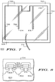
- FIG. 7 illustrates the die 600 of FIG. 6, further having a single level of metal 700 covering the die.
- portion 702 of metal layer 700 provides electrical contact to the patterned gate fingers, while portion 704 provides contiguous electrical contact to the source regions within openings 612 exposed by the polysilicon gate fingers 604, 606, 608 and 610.
- the patterned polysilicon 602 is covered with a dielectric in the areas over which portion 704 is formed, before metal layer 700 is formed. Consequently, metal layer portion 704 contacts the source regions (e.g. 612) while being insulated from the gate fingers (e.g. 604).
- metal layer portion 702 contacting the polysilicon gate fingers is electrically isolated from metal layer portion 704 contacting the source regions by gap 706.
- the layout seeks to reduce the length of the gate fingers (e.g. fingers 604), length herein meaning the distance from a furthest point on a gate finger to the gate feed network.
- the gate feed network is the portion of patterned polysilicon layer 602 which underlies metal layer portion 702 of FIG. 7. Consequently, the gate feed network includes extending feed fingers 614 and 616 and perimeter ring 618.
- the layout shown in FIG. 6 provides relatively short gate finger lengths by providing the gate feed network which includes two extending feed fingers 614, 616, along with perimeter ring 618. Given this configuration, it can be seen that all of the gate fingers comprising the "upper" portion of the die generally indicated by arrow 620 have a gate finger length of less than 1/6 of the length of die 600, since each of these gate fingers is fed from both sides and the feed fingers divide the die into thirds. Note that gate fingers represented by fingers 610 are advantageously much smaller due to polysilicon portion 622 which underlies metal portion 706 (FIG. 7), which is provided for attaching a wire bond during packaging of die 600.
- metal layer portion 704 would be segmented into three separate, non-contiguous and non-electrically connected portions. It must be held in mind, though, that in manufacturing, it is desirable to contact the source of the device via metal layer portion 704 with a single wire bond, illustrated as wire bond 710. Consequently, metal layer portion 704 must be contiguous.
- a second group of gate fingers in the area indicated by the arrow 622 and represented by finger 608, is provided.
- the second group of gate fingers 622 are aligned perpendicular to the first group of gate fingers 620, and are fed by perimeter ring 618 of the gate feed network along with portion 624 of the patterned polysilicon. If these gate fingers did't perpendicular, they would traverse the entire width of the device, and therefore be undesirably long. It should be noted that gate fingers generally indicated by arrows 626 are also acceptably short. Consequently, the layout illustrated by FIG. 6 provides gate fingers having lengths which are at least less than half of the longer of the length or width of die 600.
- FIG. 8 is an illustrative cross-section side view of the portion of die 600 indicated by arrows 8-8, and further including a dielectric covering the gate fingers and metal layer portion 704 (FIG. 7) covering the dielectric.
- N type semiconductor substrate 800 is provided.
- a P+ implant is carried out in order to form the P well portions 802, also referred to as the tub or base portion.
- the base portion is all one single contiguous base.
- a positive, latex based photoresist is used for the implant. Positive photoresist is desirable because it typically provides greater resolution, compared to negative photoresist. It will be recognized that it is desirable to reduce the spacing between gate fingers 804 as much as possible. Consequently, since the width of implant portions 802 limit the spacing of gate fingers 804, it is desirable to make implant portions 802 as narrow as possible.
- a gate oxide layer which forms oxide portions 806 is formed.
- a polysilicon layer which will result in gate fingers 804 is deposited over the gate oxide layer. It will be understood that both of these layers are initially formed as continuous sheets, and the fingers are defined later by etching.
- the polysilicon layer is patterned to form the gate fingers.
- the gate fingers 804 well known etching techniques are used. However, as in the previously discussed masking step, positive photoresist is used again in order to provide more fine definition than is available with negative photoresist.
- the gate oxide layer which will underlie the gate fingers is initially left as a conformal coating through which the implants (P- channel, N+ source) are performed.
- a mask is defined through which source regions 810 are implanted. It should be recalled that, in certain preferred embodiments, the mask through which end type source regions 810 are implanted is configured such that certain adjacent source regions are cross connected, as illustrated in FIG. 4. Furthermore, in certain preferred applications, the photolithography processing for implanting N+ source regions 810 utilizes positive photoresist in order to achieve fine geometry.
- gate oxide portions 806 and dielectric 814 is patterned at this step. Again, positive photoresist is employed in order to achieve the fine geometry needed considering the extremely small stripe spacing.
- FIG. 9 is a magnified view of portion 9 shown in FIG. 6, particularly illustrating the layout of the implant for forming P+ regions 802 (which can also be seen in FIG. 8) with reference to patterned polysilicon layers 602 (from FIG. 6), including gate fingers 804 (from FIG. 8).
- FIG. 9 illustrates an important feature with respect to implant layer 900 which includes regions 802. More specifically, all of the "corners”, e.g., corners 902, are "inside corners” that is, the entire layer 900 is designed (laid out) so that there are no open ended stubs (outside corners), but rather only inside corners 902 throughout the layout.
- the reason for this inside corner layout is related to the fact that, as is well known, the base resistance of the transistor is directly related to the P+ implant doping concentration.
- the P impurities at an inside corner will tend to defuse in an overlapping fashion. Consequently, the P+ doping concentrations at the corners will increase, thereby reducing base resistance in the corner areas.
- a transistor has been provided which can provide the advantages of efficient and effective device layout, improved energy, breakdown voltage, lower on-resistace, lower capacitance and higher packing density.
Landscapes
- Insulated Gate Type Field-Effect Transistor (AREA)
- Electrodes Of Semiconductors (AREA)
- Metal-Oxide And Bipolar Metal-Oxide Semiconductor Integrated Circuits (AREA)
Abstract

Description
- The present invention relates to semiconductor devices, and more particularly to transistors having common base regions and transistors having efficient and effective layout.
- In the past, vertical-type transistors such as power MOSFETs (Metal Oxide Silicon Field Effect Transistor) have comprised discrete and separate base region cells which define discrete and separate active regions. In a typical device die comprising many of such regions, the regions are electrically coupled together so that they act as a single transistor. Seperate cells give rise to certain disadvantages. For example, the base-emitter region of every cell must be shorted for maximum energy. In addition, cell corners have adverse effects on breakdown voltage.
- Furthermore, transistor configurations which are alternative to cells, such as stripes, have given rise to particular disadvantages. For example, striped-layout transistors inherently comprise elongated gate fingers. Electrical contact must be made to these elongated gate fingers in order to turn on or turn off the transistor. Conventionally, electrical connection to the elongated gate fingers are made at their extreme ends. Contacting the gate fingers at their ends creates a resistance to the gate finger which varies along its length. Consequently, the transistor's performance characteristics vary along the length of the gate finger. It will be recognized by those skilled in the art that this condition is undesirable.
- Consequently, what is needed is a transistor which avoids the problem of individual, seperate cells. Furthermore, what is needed is a transistor which has an efficient and effective layout such that transistor performance parameters do not vary materially at different locations of the device.
-
- FIG. 1 is a simplified cross-sectional view of a vertical MOS transistor in accordance with one embodiment of the present invention;
- FIG. 2 is a simplified top view of a transistor in accordance with one embodiment of the present invention;
- FIG. 3 is a simplified cross-sectional view of an alternative embodiment of a transistor in accordance with the present invention;
- FIG. 4 is a partial top view of an alternative embodiment of a transistor in accordance with the present invention;
- FIG. 5 is a simplified cross-sectional view of an alternative embodiment of a transistor in accordance with the present invention;
- FIG. 6 is a simplified top view illustrating the layout of a transistor die including patterned polysilicon forming gate fingers;
- FIG. 7 is a top view of the semiconductor die of FIG. 6 further including a metal level;
- FIG. 8 is a simplified cross-section view representing a portion of a transistor; and
- FIG. 9 is an enlarged view of a portion of FIG. 6.
- Generally stated, one preferred embodiment of the present invention is a Metal Oxide Silicon Field Effect Transistor (MOSFET) which has a single common "base region". The base region is sometimes referred to, by those with average knowledge of the industry, as a body region, tub or well. In an enhancement mode N-channel MOSFET, which is typical in the industry, the base region is the region of the structure which is P+ and P-doped to provide the channel region for the field effect transistor. Additionally, it will be understood by those with average knowledge of the industry that similar technology applies to Insulated Gate Bipolar Transistors (IGBT) and P channel MOSFETS, as well. The device with a single common base region eliminates the exterior corners found in seperate cell devices, thereby imrpoving breakdown voltage. Additionally, the single common base region device reduces the probability of open base avalanche injection.
- Turning to the figures for a more detailed understanding, FIG. 1 is a simplified cross-section of a portion of a MOSFET in accordance with one embodiment of the present invention. More specifically,
MOSFET 100 is a vertically stacked semiconductor structure.Transistor 100 is an enhancement mode N-channel MOSFET.Transistor 100 comprises N⁺-type substrate 102. N-typeepitaxial layer 104 is grown to a sufficient thickness onsubstrate 102 in accordance with methods well known in the industry. - P-
type regions 106 are part of a larger common base region which will be further illustrated in the top view of FIG. 2. P-type region 106 comprises P⁺-region 108, the lower lobe of the region, and P-region 110, the upper lobe of the region. -
Transistor 100 further comprisessource regions 112 which are N⁺-type doped.Source regions 112 reside generally in theupper lobe region 110 of thecommon base region 106. - Additionally,
transistor 100 includes N-dopedlayer 114 which improves certain operating parameters.Layer 114 is sometimes referred to as the pre-gate implant layer because it is formed prior to forming the gate of the device. The N-type doping ofregions 112 andlayer 114 are considered a first dopant type. Specifically,layer 114 reduces the on-resistance of the transistor. -
Oxide portion 116 resides on afirst surface 118 oftransistor 100. The edges ofoxide layer 116 overlapupper lobe portions 110 ofcommon base region 106, as well assource regions 112.Gate portion 120overlies oxide portion 116. Those with average knowledge of the industry will be quite familiar with the operation of the MOSFET illustrated in FIG. 1, as well as the process technologies available for fabricating the device illustrated. It will be understood thattransistor 100 conducts current vertically betweenfirst surface 118 andsecond surface 122, which is the bottom surface and is parallel tofirst surface 118. - Turning to FIG. 2, FIG. 2 particularly illustrates one of the important novel features of the embodiment of the present invention being described. More specifically, FIG. 2 is a simplified top view of a transistor 200 in accordance with one embodiment of the present invention. Transistor 200 includes the
transistor portion 100 shown in FIG. 1, as indicated by the dashed line marked with thenumber 1. Transistor 200 comprises singlecommon base region 202. Singlecommon base region 202 includes P⁺-type portions 204 as well as P-type portions 206. The lines of FIG. 2 definingregions 206 merely indicate a transition between of P-type concentration, from P+ to P-. Referring briefly back to FIG. 1 for a better understanding, P⁺-type portions 204 make uplower lobes 108 ofbase region 106. Furthermore, P-type portions 206 make upupper lobes 110 ofbase region 106. Additionally,source regions 112 can be seen from the top view in FIG. 2. Furthermore,gate 120 is shown in top view, in FIG. 2. - The gate of
transistor portion 208 has been left off of FIG. 2 so as to reveal details below the gate. More specifically, anepitaxial portion 210 is revealed. Referring again to FIG. 1, anepitaxial portion 210 is analogous toportion 124, centered belowgate 120. - Certain notable features of transistor 200 in accordance with one embodiment of the present invention are revealed by the top view shown in FIG. 2. Specifically, transistor 200 comprises a single
common base region 202 having several small regions where epitaxial portions (e.g., portion 210) are revealed. Due to the geometry of this particular embodiment, singlecommon base region 202 is considered a striped base region. The stripes are considered to run vertically in the figure, betweenepitaxial portions 210. Transistor 200, and similar transistors, comprise at least two of these elongated base portions, or stripes. The stripes are joined integrally bybase region border 212.Base region border 212 is the rectangular shaped outer edge ofcommon base region 202. - Referring to FIG. 2,
source regions 112 are formed inportions 208 ofcommon base region 202. More specifically, in the embodiment shown,source regions 112 are opposing parallel elongated regions. -
Overlying base region 202 andsource regions 112 aregate regions 120. In the embodiment shown,gate regions 120 comprise elongated gate regions or gate fingers. - FIG. 3 is a simplified cross section of an alternative embodiment of a
portion 208 of transistor 200. One notable distinction between the embodiment shown in FIG. 3 and the embodiment shown in FIG. 1 is the configuration ofoxide layer 316.Oxide layer 316 has acentral portion 318 andedge portions 319.Central portion 318 is higher thanedge portions 319. The configuration ofgate oxide layer 316 is achieved with well known processing techniques.Polysilicon gate 320 is formed overgate oxide layer 316. Due to the shape ofgate oxide layer 316,polysilicon gate 320 includes a raisedcentral portion 321 andedge portions 322.Central portion 321 is higher thanedge portions 322. - The configuration of the
gate oxide layer 316 andpolysilicon gate 320 provides the advantage of reduced gate to drain capacitance for the device. It will be understood by those with average knowledge of the industry that the drain is considered to be an electrical contact on thebottom surface 324 of the device. Additionally, the configuration oflayer 316 andgate 321 has the effect of causingpre-gate implant layer 326 to be discontinuous beneath thecentral portion 321 ofgate 320. This discontinuity in the region beneath the center of the gate provides improved operation parameters as well. For example, improved on-resistance in high voltage devices is achieved. - FIG. 4 illustrates an alternative embodiment of a transistor in accordance with the present invention. More specifically,
transistor 400 of FIG. 4 is very similar to transistor 200 of FIG. 2, however, certain adjacent source regions are cross connected. More specifically,elongated source regions 402 are cross connected with adjacent elongated source regions byregions 404.Regions 404 are N⁺-type doped regions similar in nature to theelongated source regions 402. The advantages provided by the cross connected source regions are illustrated by FIG. 5. - FIG. 5 is a cross section of a portion of a transistor consistent with the layout in FIG. 4. More specifically, FIG. 5 shows two device portions, 500 and 502. The structure of FIG. 5 is very similar to the structure of FIG. 1. Furthermore, FIG. 5 additionally shows an insulating oxide layer 504 covering
polysilicon gates 506. On top of insulating oxide layer 504 ismetal layer 508. As will be well understood by those with average knowledge of the industry,metal layer 508 provides the source electrode of the device. Consequently, it will be recognized that it is important thatmetal layer 508 contact elongatedsource regions 510. - As the density of the device increases, there will be less room available to lengthen
elongated source regions 510 in the general area betweentransistor portions metal layer 508 is required. Consequently, thecross connecting regions 512 are provided.Cross connecting regions 512 allow for sufficient and substantial electrical contact frommetal layer 508 toelongated source regions 510. Consequently, higher packing densities can be achieved. - Turning now to FIG. 6, FIG. 6 illustrates a particularly efficient and effective layout of an entire transistor die in accordance with the present invention. In order to best illustrate the layout of the die, FIG. 6 shows the patterned
polysilicon 602 making the gate fingers, represented bygate fingers gate finger 604 of FIG. 6 corresponds togate finger 120 of FIG. 2. Anopening 612 in the patternedpolysilicon 602 of thedie 600 corresponds to the opening in FIG. 2 between the twogate fingers 120. Referring to FIG. 2, it can be seen that this opening exposessource regions 112. However, for the sake of clarity, the detail of the source regions such as 112 in FIG. 2 is not shown within theopening 612 of FIG. 6. Nevertheless, it will be understood that such source regions are exposed by theopenings 612 throughout the patternedpolysilicon 602. - Returning to FIG. 6 for an understanding of the particularities of the layout, it will be understood by those skilled in the art that, in order to operate the transistor device of
die 600, electrical contact must be made to all of the gate fingers represented byfingers polysilicon 602 represented by opening 612. Additionally, it will be recognized that a third "drain" electrical contact must be made to the bottom surface ofdie 600, not shown. In order to simplify and reduce the cost of manufacturing the die, it is desirable to provide electrical contact to the gate fingers and to the source contact regions between the gate fingers with the same single level of metal. This idea is better understood with reference to FIG. 7. - FIG. 7 illustrates the
die 600 of FIG. 6, further having a single level ofmetal 700 covering the die. With reference to both FIGs. 6 and 7, it can be seen thatportion 702 ofmetal layer 700 provides electrical contact to the patterned gate fingers, whileportion 704 provides contiguous electrical contact to the source regions withinopenings 612 exposed by thepolysilicon gate fingers polysilicon 602 is covered with a dielectric in the areas over whichportion 704 is formed, beforemetal layer 700 is formed. Consequently,metal layer portion 704 contacts the source regions (e.g. 612) while being insulated from the gate fingers (e.g. 604). Furthermore, it can be seen thatmetal layer portion 702 contacting the polysilicon gate fingers is electrically isolated frommetal layer portion 704 contacting the source regions bygap 706. - Returning to FIG. 6 for further explanation of the layout, it can be seen that the layout seeks to reduce the length of the gate fingers (e.g. fingers 604), length herein meaning the distance from a furthest point on a gate finger to the gate feed network. The gate feed network is the portion of patterned
polysilicon layer 602 which underliesmetal layer portion 702 of FIG. 7. Consequently, the gate feed network includes extendingfeed fingers perimeter ring 618. - It is desirable to reduce the length of the gate fingers, because the resistance of the gate finger increases along its length. Consequently, the operating parameters of the transistor will correspondingly vary along the length of the gate finger. Therefore, gate finger lengths must be reduced to the point where there is no material variance of transistor operating parameters along the length of the gate fingers.
- The layout shown in FIG. 6 provides relatively short gate finger lengths by providing the gate feed network which includes two extending
feed fingers perimeter ring 618. Given this configuration, it can be seen that all of the gate fingers comprising the "upper" portion of the die generally indicated byarrow 620 have a gate finger length of less than 1/6 of the length ofdie 600, since each of these gate fingers is fed from both sides and the feed fingers divide the die into thirds. Note that gate fingers represented byfingers 610 are advantageously much smaller due to polysilicon portion 622 which underlies metal portion 706 (FIG. 7), which is provided for attaching a wire bond during packaging ofdie 600. - Given that the first group of gate fingers in
upper portion 620 are of appropriate length for good performance of the transistor, it might be questioned as to why feedfingers feed fingers die 600 thenmetal layer portion 704 would be segmented into three separate, non-contiguous and non-electrically connected portions. It must be held in mind, though, that in manufacturing, it is desirable to contact the source of the device viametal layer portion 704 with a single wire bond, illustrated aswire bond 710. Consequently,metal layer portion 704 must be contiguous. - Returning to FIG. 6, it should now be understood why a second group of gate fingers in the area indicated by the arrow 622 and represented by
finger 608, is provided. The second group of gate fingers 622 are aligned perpendicular to the first group ofgate fingers 620, and are fed byperimeter ring 618 of the gate feed network along withportion 624 of the patterned polysilicon. If these gate fingers weren't perpendicular, they would traverse the entire width of the device, and therefore be undesirably long. It should be noted that gate fingers generally indicated byarrows 626 are also acceptably short. Consequently, the layout illustrated by FIG. 6 provides gate fingers having lengths which are at least less than half of the longer of the length or width ofdie 600. - Turning now to FIGs. 8 and 9, FIGs. 8 and 9 illustrate certain advantageous methods for manufacturing the transistor die 600. FIG. 8 is an illustrative cross-section side view of the portion of
die 600 indicated by arrows 8-8, and further including a dielectric covering the gate fingers and metal layer portion 704 (FIG. 7) covering the dielectric. Although one of ordinary skill in the art will recognize various methods for arriving at the device shown, the process is generally described here in order to point out certain advantageous ways of carrying out certain steps. Furthermore, only relevant steps will be discussed, and it will be understood that there are intervening steps which are well known in the art. - Accordingly to one preferred embodiment, N
type semiconductor substrate 800 is provided. Initially, a P+ implant is carried out in order to form the P wellportions 802, also referred to as the tub or base portion. As discussed in detail earlier, the base portion is all one single contiguous base. One notable feature of the implant is that a positive, latex based photoresist is used for the implant. Positive photoresist is desirable because it typically provides greater resolution, compared to negative photoresist. It will be recognized that it is desirable to reduce the spacing betweengate fingers 804 as much as possible. Consequently, since the width ofimplant portions 802 limit the spacing ofgate fingers 804, it is desirable to makeimplant portions 802 as narrow as possible. - After implanting
portions 802, a gate oxide layer which formsoxide portions 806 is formed. Subsequently, a polysilicon layer which will result ingate fingers 804 is deposited over the gate oxide layer. It will be understood that both of these layers are initially formed as continuous sheets, and the fingers are defined later by etching. - Next, the polysilicon layer is patterned to form the gate fingers. In order to define the
gate fingers 804 well known etching techniques are used. However, as in the previously discussed masking step, positive photoresist is used again in order to provide more fine definition than is available with negative photoresist. The gate oxide layer which will underlie the gate fingers is initially left as a conformal coating through which the implants (P- channel, N+ source) are performed. - Subsequent to implanting
portions 808, a mask is defined through whichsource regions 810 are implanted. It should be recalled that, in certain preferred embodiments, the mask through which endtype source regions 810 are implanted is configured such that certain adjacent source regions are cross connected, as illustrated in FIG. 4. Furthermore, in certain preferred applications, the photolithography processing for implantingN+ source regions 810 utilizes positive photoresist in order to achieve fine geometry. - Further photolithographic processing is conducted in order to provide the preohmic for metal contact to source
regions 810,P tub regions 802, and gate polysilicon.Gate oxide portions 806 and dielectric 814 is patterned at this step. Again, positive photoresist is employed in order to achieve the fine geometry needed considering the extremely small stripe spacing. - One of the final steps, as will be recognized by those of ordinarily skill in the art, is the deposition of aluminum 812, which provides ohmic contact to the
source regions 810 andP tub regions 802. - Turning to FIG. 9, FIG. 9 is a magnified view of portion 9 shown in FIG. 6, particularly illustrating the layout of the implant for forming P+ regions 802 (which can also be seen in FIG. 8) with reference to patterned polysilicon layers 602 (from FIG. 6), including gate fingers 804 (from FIG. 8). FIG. 9 illustrates an important feature with respect to
implant layer 900 which includesregions 802. More specifically, all of the "corners", e.g.,corners 902, are "inside corners" that is, theentire layer 900 is designed (laid out) so that there are no open ended stubs (outside corners), but rather only insidecorners 902 throughout the layout. The reason for this inside corner layout is related to the fact that, as is well known, the base resistance of the transistor is directly related to the P+ implant doping concentration. When theimplant layer 900 is implanted, and subsequently diffused during normal device fabrication, the P impurities at an inside corner will tend to defuse in an overlapping fashion. Consequently, the P+ doping concentrations at the corners will increase, thereby reducing base resistance in the corner areas. If, on the other hand,implant layer 900 included open ended stubs (outside corners) the P+ implant would thin out as it diffused. The diminishing P+ implant would increase base resistance, tending to cause device failure in the isolated areas where the P+ implant thins. - By now it will be appreciated that a transistor has been provided which can provide the advantages of efficient and effective device layout, improved energy, breakdown voltage, lower on-resistace, lower capacitance and higher packing density.
- While we have shown and described specific illustrative embodiments of the present invention, further modifications and improvements will occur to those skilled in the art. We desire it to be understood, therefore, that this invention is not limited to the particular forms shown and we intend in the appended claims to cover all modifications that do not depart from the spirit and scope of this invention.
Claims (11)
- A transistor comprising:
a vertically stacked semiconductor structure (100) comprising a first surface (118) and a second surface (122) parallel to the first surface (118), the transistor configured to conduct current from the first surface (118) to the second surface (122);
a single common base region (202); and
one or more source regions (112) comprising a first material, the one or more source regions formed in the single common base region (202), wherein certain adjacent ones of the one or more source regions (112) are cross-connected (404) with the first material. - A transistor comprising:
a common base region (202);
one or more source regions (112) formed in the common base region (202); and
one or more gate regions (120) overlying the common base region (202) and the one or more source regions (112), wherein each of the gate regions (120) comprises an elongated gate finger (320) having a cross-section, the cross-section having a central portion (321) and edge portions (322), and wherein the central portion (321) is thicker than the edge portions (322). - The transistor of claim 2, further comprising a pre-gate implant layer (326) beneath the one or more gate regions (320), the pre-gate implant layer (326) discontinuous in areas beneath the central (321) portions of the gate regions.
- The transistor of claim 2, wherein certain adjacent ones of the one or more source regions (402) are cross connected (404).
- A vertical transistor comprising:
a common striped base region (202);
a plurality of elongated source regions (510) comprising a first doped material, the plurality of source regions (510) formed in the common striped base region (202), certain adjacent ones of the source regions (510) being cross-connected (512) with the first doped material; and
one or more gate fingers (120) overlying the common striped base region (202) and the one or more source regions (510). - The vertical transistor of claim 5, wherein each of the one or more gate fingers (120) comprises a central portion (321) and edge portions (322), the central portion (321) being higher than the edge portions (322).
- A transistor comprising:
a semiconductor die (600) having a length and a width;
a patterned gate region (602) comprising a plurality of gate fingers (604,606,608,610), the patterned gate region (602) exposing a plurality of source contact regions (112);
a gate feed network (614,616,618);
each of the plurality of gate fingers (604,606,608,610) having a gate finger length which is a distance from a furthest point on the gate finger to the gate feed network (614,616,618);
a single metal level (700) contacting the gate feed network (614,616,618) and the plurality of source contact regions (112), the gate feed (614,616,618) network being electrically isolated from the plurality of source contact regions (112), the plurality of source contact regions (112) being contiguously electrically coupled; and
wherein a maximum gate finger length is less than one half of the larger of the semiconductor die length and width. - The transistor of Claim 7, wherein the plurality of gate fingers (604,606,608,610) comprises a first group of gate fingers (620) aligned in a first direction and a second group of gate fingers (622) aligned in a second direction perpendicular to the first direction.
- The transistor of Claim 8, wherein the gate feed network (614,616,618) comprises a perimeter ring (618) and at least one extending feed finger (614), the extending feed finger (614) feeding the first group of gate fingers (620) and the perimeter ring (618) feeding the second group (622) of gate fingers.
- A transistor comprising:
a plurality of source regions (112) interspersed in a plurality of parallel aligned gate fingers (604,606,608,610);
a single metal level (700) providing electrical contact to both the plurality of source contact regions (112) and the plurality of gate fingers (604,606,608,610), the plurality of source regions (112) being contiguously electrically coupled; and
a single external electrical contact (710) contacting the plurality of source regions (112) via a portion of the single level of metal (704). - The transistor of Claim 10, wherein the plurality of gate fingers (604,606,608,610) comprises a first group of gate fingers (620) aligned in a first direction and a second group of gate fingers (622) aligned in a second direction perpendicular to the first direction.
Priority Applications (1)
| Application Number | Priority Date | Filing Date | Title |
|---|---|---|---|
| EP97120065A EP0827209A1 (en) | 1993-11-22 | 1994-11-14 | Gate layout of a transistor with common base region |
Applications Claiming Priority (4)
| Application Number | Priority Date | Filing Date | Title |
|---|---|---|---|
| US15550493A | 1993-11-22 | 1993-11-22 | |
| US272899 | 1994-07-08 | ||
| US08/272,899 US5396097A (en) | 1993-11-22 | 1994-07-08 | Transistor with common base region |
| US155504 | 2002-05-23 |
Publications (2)
| Publication Number | Publication Date |
|---|---|
| EP0655787A2 true EP0655787A2 (en) | 1995-05-31 |
| EP0655787A3 EP0655787A3 (en) | 1995-08-16 |
Family
ID=26852373
Family Applications (2)
| Application Number | Title | Priority Date | Filing Date |
|---|---|---|---|
| EP97120065A Withdrawn EP0827209A1 (en) | 1993-11-22 | 1994-11-14 | Gate layout of a transistor with common base region |
| EP94117926A Withdrawn EP0655787A3 (en) | 1993-11-22 | 1994-11-14 | Transistor with common base region. |
Family Applications Before (1)
| Application Number | Title | Priority Date | Filing Date |
|---|---|---|---|
| EP97120065A Withdrawn EP0827209A1 (en) | 1993-11-22 | 1994-11-14 | Gate layout of a transistor with common base region |
Country Status (6)
| Country | Link |
|---|---|
| US (1) | US5396097A (en) |
| EP (2) | EP0827209A1 (en) |
| JP (1) | JPH07193243A (en) |
| KR (1) | KR950015830A (en) |
| CN (1) | CN1034841C (en) |
| SG (1) | SG43005A1 (en) |
Cited By (1)
| Publication number | Priority date | Publication date | Assignee | Title |
|---|---|---|---|---|
| US7800135B2 (en) | 2005-07-25 | 2010-09-21 | Jean-Michel Reynes | Power semiconductor device and method of manufacturing a power semiconductor device |
Families Citing this family (14)
| Publication number | Priority date | Publication date | Assignee | Title |
|---|---|---|---|---|
| US6603173B1 (en) | 1991-07-26 | 2003-08-05 | Denso Corporation | Vertical type MOSFET |
| US5723890A (en) * | 1994-01-07 | 1998-03-03 | Fuji Electric Co., Ltd. | MOS type semiconductor device |
| US5703389A (en) * | 1995-02-24 | 1997-12-30 | Motorola, Inc. | Vertical IGFET configuration having low on-resistance and method |
| EP0823735A1 (en) * | 1996-08-05 | 1998-02-11 | Sgs-Thomson Microelectronics S.A. | MOS-technology power device |
| AU1211301A (en) * | 1999-10-22 | 2001-05-08 | Semiconductor Components Industries, L.L.C. | Semiconductor device with a single base region and method therefor |
| US6545543B2 (en) * | 2001-07-06 | 2003-04-08 | Remec, Inc. | Small aspect ratio MMIC power amplifier layout |
| US6870221B2 (en) * | 2002-12-09 | 2005-03-22 | Semiconductor Components Industries, Llc | Power switching transistor with low drain to gate capacitance |
| JP4474563B2 (en) * | 2002-12-26 | 2010-06-09 | 旭精工株式会社 | Bimetal coin detection device |
| JP4802306B2 (en) * | 2003-12-01 | 2011-10-26 | オンセミコンダクター・トレーディング・リミテッド | Semiconductor device |
| KR100687108B1 (en) * | 2005-05-31 | 2007-02-27 | 라이톤 세미컨덕터 코퍼레이션 | High power semiconductor device that can suppress turn-on of parasitic bipolar transistors |
| US7595523B2 (en) * | 2007-02-16 | 2009-09-29 | Power Integrations, Inc. | Gate pullback at ends of high-voltage vertical transistor structure |
| US8723177B2 (en) | 2011-12-06 | 2014-05-13 | Globalfoundries Inc. | Electrical test structure for devices employing high-k dielectrics or metal gates |
| US9543396B2 (en) | 2013-12-13 | 2017-01-10 | Power Integrations, Inc. | Vertical transistor device structure with cylindrically-shaped regions |
| US10325988B2 (en) | 2013-12-13 | 2019-06-18 | Power Integrations, Inc. | Vertical transistor device structure with cylindrically-shaped field plates |
Family Cites Families (23)
| Publication number | Priority date | Publication date | Assignee | Title |
|---|---|---|---|---|
| JPS53128281A (en) * | 1977-04-15 | 1978-11-09 | Hitachi Ltd | Insulated gate field effect type semiconductor device for large power |
| US4135289A (en) * | 1977-08-23 | 1979-01-23 | Bell Telephone Laboratories, Incorporated | Method for producing a buried junction memory device |
| US4212684A (en) * | 1978-11-20 | 1980-07-15 | Ncr Corporation | CISFET Processing including simultaneous doping of silicon components and FET channels |
| US4210465A (en) * | 1978-11-20 | 1980-07-01 | Ncr Corporation | CISFET Processing including simultaneous implantation of spaced polycrystalline silicon regions and non-memory FET channel |
| US4236166A (en) * | 1979-07-05 | 1980-11-25 | Bell Telephone Laboratories, Incorporated | Vertical field effect transistor |
| US4593302B1 (en) * | 1980-08-18 | 1998-02-03 | Int Rectifier Corp | Process for manufacture of high power mosfet laterally distributed high carrier density beneath the gate oxide |
| DE3040775C2 (en) * | 1980-10-29 | 1987-01-15 | Siemens AG, 1000 Berlin und 8000 München | Controllable MIS semiconductor device |
| US4412242A (en) * | 1980-11-17 | 1983-10-25 | International Rectifier Corporation | Planar structure for high voltage semiconductor devices with gaps in glassy layer over high field regions |
| JPS58171861A (en) * | 1982-04-01 | 1983-10-08 | Toshiba Corp | Semiconductor device |
| US4672407A (en) * | 1984-05-30 | 1987-06-09 | Kabushiki Kaisha Toshiba | Conductivity modulated MOSFET |
| US4646117A (en) * | 1984-12-05 | 1987-02-24 | General Electric Company | Power semiconductor devices with increased turn-off current ratings and limited current density in peripheral portions |
| US4809045A (en) * | 1985-09-30 | 1989-02-28 | General Electric Company | Insulated gate device |
| US4860072A (en) * | 1986-03-05 | 1989-08-22 | Ixys Corporation | Monolithic semiconductor device and method of manufacturing same |
| JPH0758782B2 (en) * | 1986-03-19 | 1995-06-21 | 株式会社東芝 | Semiconductor device |
| US5231474A (en) * | 1986-03-21 | 1993-07-27 | Advanced Power Technology, Inc. | Semiconductor device with doped electrical breakdown control region |
| US4823176A (en) * | 1987-04-03 | 1989-04-18 | General Electric Company | Vertical double diffused metal oxide semiconductor (VDMOS) device including high voltage junction exhibiting increased safe operating area |
| JPS6449273A (en) * | 1987-08-19 | 1989-02-23 | Mitsubishi Electric Corp | Semiconductor device and its manufacture |
| JPH02133966A (en) * | 1988-11-14 | 1990-05-23 | Fuji Electric Co Ltd | Field effect transistor |
| JPH077750B2 (en) * | 1989-05-15 | 1995-01-30 | 株式会社東芝 | Method for manufacturing semiconductor device |
| US5208471A (en) * | 1989-06-12 | 1993-05-04 | Hitachi, Ltd. | Semiconductor device and manufacturing method therefor |
| US5313088A (en) * | 1990-09-19 | 1994-05-17 | Nec Corporation | Vertical field effect transistor with diffused protection diode |
| US5304831A (en) * | 1990-12-21 | 1994-04-19 | Siliconix Incorporated | Low on-resistance power MOS technology |
| JPH05206470A (en) * | 1991-11-20 | 1993-08-13 | Nec Corp | Insulated gate field effect transistor |
-
1994
- 1994-07-08 US US08/272,899 patent/US5396097A/en not_active Expired - Lifetime
- 1994-11-14 SG SG1996002157A patent/SG43005A1/en unknown
- 1994-11-14 EP EP97120065A patent/EP0827209A1/en not_active Withdrawn
- 1994-11-14 EP EP94117926A patent/EP0655787A3/en not_active Withdrawn
- 1994-11-21 CN CN94118713A patent/CN1034841C/en not_active Expired - Fee Related
- 1994-11-21 JP JP6309435A patent/JPH07193243A/en active Pending
- 1994-11-22 KR KR1019940030710A patent/KR950015830A/en not_active Ceased
Cited By (1)
| Publication number | Priority date | Publication date | Assignee | Title |
|---|---|---|---|---|
| US7800135B2 (en) | 2005-07-25 | 2010-09-21 | Jean-Michel Reynes | Power semiconductor device and method of manufacturing a power semiconductor device |
Also Published As
| Publication number | Publication date |
|---|---|
| CN1034841C (en) | 1997-05-07 |
| JPH07193243A (en) | 1995-07-28 |
| EP0827209A1 (en) | 1998-03-04 |
| KR950015830A (en) | 1995-06-17 |
| SG43005A1 (en) | 1997-10-17 |
| EP0655787A3 (en) | 1995-08-16 |
| CN1108814A (en) | 1995-09-20 |
| US5396097A (en) | 1995-03-07 |
Similar Documents
| Publication | Publication Date | Title |
|---|---|---|
| US7005347B1 (en) | Structures of and methods of fabricating trench-gated MIS devices | |
| US5447876A (en) | Method of making a diamond shaped gate mesh for cellular MOS transistor array | |
| US5396097A (en) | Transistor with common base region | |
| US10861965B2 (en) | Power MOSFET with an integrated pseudo-Schottky diode in source contact trench | |
| US20030057478A1 (en) | Mos-gated power semiconductor device | |
| US20030040144A1 (en) | Trench DMOS transistor with embedded trench schottky rectifier | |
| US20080179672A1 (en) | Lateral semiconductor component with a drift zone having at least one field electrode | |
| US6030870A (en) | High density MOS technology power device | |
| CN110581069B (en) | Method for manufacturing a high voltage semiconductor device | |
| US6486512B2 (en) | Power semiconductor device having high breakdown voltage and method for fabricating the same | |
| CN110957370A (en) | Manufacturing method of lateral double diffused transistor | |
| US6344379B1 (en) | Semiconductor device with an undulating base region and method therefor | |
| JP3448138B2 (en) | Method for manufacturing semiconductor device | |
| US6664595B1 (en) | Power MOSFET having low on-resistance and high ruggedness | |
| US6635926B2 (en) | Field effect transistor with high withstand voltage and low resistance | |
| EP0823735A1 (en) | MOS-technology power device | |
| CN115472681A (en) | Self-aligned double-groove shielded gate MOSFET structure and its manufacturing method | |
| US20210305242A1 (en) | Power device including lateral insulated gate bipolar transistor (ligbt) and manufacturing method thereof | |
| US6215167B1 (en) | Power semiconductor device employing field plate and manufacturing method thereof | |
| JPH01292862A (en) | Semiconductor device | |
| US20250212485A1 (en) | Power semiconductor devices | |
| CN110010685A (en) | Groove metal-oxide-semiconductor element and its manufacturing method | |
| CN119170643A (en) | Transistor structure and manufacturing method thereof | |
| CN118676207A (en) | Semiconductor device and method for manufacturing semiconductor device | |
| WO2001031709A1 (en) | Semiconductor device with a single base region and method therefor |
Legal Events
| Date | Code | Title | Description |
|---|---|---|---|
| PUAI | Public reference made under article 153(3) epc to a published international application that has entered the european phase |
Free format text: ORIGINAL CODE: 0009012 |
|
| AK | Designated contracting states |
Kind code of ref document: A2 Designated state(s): DE FR GB IT |
|
| RIN1 | Information on inventor provided before grant (corrected) |
Inventor name: GROENIG, PAUL J. Inventor name: FRAGALE, WILLIAM L. Inventor name: ROBB, STEPHEN P. |
|
| PUAL | Search report despatched |
Free format text: ORIGINAL CODE: 0009013 |
|
| AK | Designated contracting states |
Kind code of ref document: A3 Designated state(s): DE FR GB IT |
|
| 17P | Request for examination filed |
Effective date: 19960216 |
|
| 17Q | First examination report despatched |
Effective date: 19970429 |
|
| STAA | Information on the status of an ep patent application or granted ep patent |
Free format text: STATUS: THE APPLICATION IS DEEMED TO BE WITHDRAWN |
|
| 18D | Application deemed to be withdrawn |
Effective date: 19990212 |