EP1909080B1 - Ultrasensibler optischer Detektor mit hoher zeitlicher Auflösung basierend auf einem Gitter. - Google Patents
Ultrasensibler optischer Detektor mit hoher zeitlicher Auflösung basierend auf einem Gitter. Download PDFInfo
- Publication number
- EP1909080B1 EP1909080B1 EP07117593A EP07117593A EP1909080B1 EP 1909080 B1 EP1909080 B1 EP 1909080B1 EP 07117593 A EP07117593 A EP 07117593A EP 07117593 A EP07117593 A EP 07117593A EP 1909080 B1 EP1909080 B1 EP 1909080B1
- Authority
- EP
- European Patent Office
- Prior art keywords
- lines
- optical detector
- anyone
- nbn
- grating
- Prior art date
- Legal status (The legal status is an assumption and is not a legal conclusion. Google has not performed a legal analysis and makes no representation as to the accuracy of the status listed.)
- Not-in-force
Links
- 230000003287 optical effect Effects 0.000 title claims description 45
- 230000002123 temporal effect Effects 0.000 title description 3
- 238000010521 absorption reaction Methods 0.000 claims abstract description 27
- 239000003989 dielectric material Substances 0.000 claims abstract description 9
- 239000000758 substrate Substances 0.000 claims description 39
- WYTGDNHDOZPMIW-RCBQFDQVSA-N alstonine Natural products C1=CC2=C3C=CC=CC3=NC2=C2N1C[C@H]1[C@H](C)OC=C(C(=O)OC)[C@H]1C2 WYTGDNHDOZPMIW-RCBQFDQVSA-N 0.000 claims description 18
- 239000000463 material Substances 0.000 claims description 15
- 239000011159 matrix material Substances 0.000 claims description 6
- 239000007788 liquid Substances 0.000 claims description 4
- 239000007787 solid Substances 0.000 claims description 3
- 230000000737 periodic effect Effects 0.000 claims description 2
- 230000010287 polarization Effects 0.000 abstract description 12
- CFJRGWXELQQLSA-UHFFFAOYSA-N azanylidyneniobium Chemical compound [Nb]#N CFJRGWXELQQLSA-UHFFFAOYSA-N 0.000 description 70
- 238000001514 detection method Methods 0.000 description 21
- VYPSYNLAJGMNEJ-UHFFFAOYSA-N Silicium dioxide Chemical compound O=[Si]=O VYPSYNLAJGMNEJ-UHFFFAOYSA-N 0.000 description 18
- 238000004519 manufacturing process Methods 0.000 description 17
- XUIMIQQOPSSXEZ-UHFFFAOYSA-N Silicon Chemical compound [Si] XUIMIQQOPSSXEZ-UHFFFAOYSA-N 0.000 description 14
- 238000000034 method Methods 0.000 description 12
- 229910052594 sapphire Inorganic materials 0.000 description 10
- 239000010980 sapphire Substances 0.000 description 10
- 229910052710 silicon Inorganic materials 0.000 description 10
- 239000010703 silicon Substances 0.000 description 10
- QEVHRUUCFGRFIF-MDEJGZGSSA-N reserpine Chemical compound O([C@H]1[C@@H]([C@H]([C@H]2C[C@@H]3C4=C(C5=CC=C(OC)C=C5N4)CCN3C[C@H]2C1)C(=O)OC)OC)C(=O)C1=CC(OC)=C(OC)C(OC)=C1 QEVHRUUCFGRFIF-MDEJGZGSSA-N 0.000 description 9
- 239000000377 silicon dioxide Substances 0.000 description 9
- 238000000151 deposition Methods 0.000 description 7
- 230000008878 coupling Effects 0.000 description 6
- 238000010168 coupling process Methods 0.000 description 6
- 238000005859 coupling reaction Methods 0.000 description 6
- 230000008021 deposition Effects 0.000 description 6
- 238000011049 filling Methods 0.000 description 6
- 239000010408 film Substances 0.000 description 6
- 239000002070 nanowire Substances 0.000 description 6
- 239000013307 optical fiber Substances 0.000 description 6
- 229910004298 SiO 2 Inorganic materials 0.000 description 5
- 230000015572 biosynthetic process Effects 0.000 description 5
- 229910052681 coesite Inorganic materials 0.000 description 5
- 229910052906 cristobalite Inorganic materials 0.000 description 5
- 238000005530 etching Methods 0.000 description 5
- 229910052682 stishovite Inorganic materials 0.000 description 5
- 229910052905 tridymite Inorganic materials 0.000 description 5
- 238000000407 epitaxy Methods 0.000 description 4
- 238000004377 microelectronic Methods 0.000 description 4
- 238000004458 analytical method Methods 0.000 description 3
- 230000005540 biological transmission Effects 0.000 description 3
- 239000000470 constituent Substances 0.000 description 3
- 238000013461 design Methods 0.000 description 3
- 238000011161 development Methods 0.000 description 3
- 230000005684 electric field Effects 0.000 description 3
- 239000007789 gas Substances 0.000 description 3
- 239000002784 hot electron Substances 0.000 description 3
- 238000003384 imaging method Methods 0.000 description 3
- BASFCYQUMIYNBI-UHFFFAOYSA-N platinum Chemical compound [Pt] BASFCYQUMIYNBI-UHFFFAOYSA-N 0.000 description 3
- 238000005498 polishing Methods 0.000 description 3
- 238000004088 simulation Methods 0.000 description 3
- 239000002887 superconductor Substances 0.000 description 3
- 241000238366 Cephalopoda Species 0.000 description 2
- XAGFODPZIPBFFR-UHFFFAOYSA-N aluminium Chemical compound [Al] XAGFODPZIPBFFR-UHFFFAOYSA-N 0.000 description 2
- 229910052782 aluminium Inorganic materials 0.000 description 2
- 238000013459 approach Methods 0.000 description 2
- 230000008901 benefit Effects 0.000 description 2
- 239000011248 coating agent Substances 0.000 description 2
- 238000000576 coating method Methods 0.000 description 2
- 230000000694 effects Effects 0.000 description 2
- 238000005516 engineering process Methods 0.000 description 2
- 239000000835 fiber Substances 0.000 description 2
- 230000004907 flux Effects 0.000 description 2
- PCHJSUWPFVWCPO-UHFFFAOYSA-N gold Chemical compound [Au] PCHJSUWPFVWCPO-UHFFFAOYSA-N 0.000 description 2
- 229910052737 gold Inorganic materials 0.000 description 2
- 239000010931 gold Substances 0.000 description 2
- 230000010365 information processing Effects 0.000 description 2
- 238000001459 lithography Methods 0.000 description 2
- 150000004767 nitrides Chemical class 0.000 description 2
- 230000010363 phase shift Effects 0.000 description 2
- 238000000623 plasma-assisted chemical vapour deposition Methods 0.000 description 2
- 229910021420 polycrystalline silicon Inorganic materials 0.000 description 2
- 239000004065 semiconductor Substances 0.000 description 2
- 238000004544 sputter deposition Methods 0.000 description 2
- 239000000126 substance Substances 0.000 description 2
- 230000009897 systematic effect Effects 0.000 description 2
- 239000010409 thin film Substances 0.000 description 2
- 238000012546 transfer Methods 0.000 description 2
- 241000954177 Bangana ariza Species 0.000 description 1
- ATJFFYVFTNAWJD-UHFFFAOYSA-N Tin Chemical compound [Sn] ATJFFYVFTNAWJD-UHFFFAOYSA-N 0.000 description 1
- 230000002745 absorbent Effects 0.000 description 1
- 239000002250 absorbent Substances 0.000 description 1
- 238000000862 absorption spectrum Methods 0.000 description 1
- 239000004411 aluminium Substances 0.000 description 1
- PNEYBMLMFCGWSK-UHFFFAOYSA-N aluminium oxide Inorganic materials [O-2].[O-2].[O-2].[Al+3].[Al+3] PNEYBMLMFCGWSK-UHFFFAOYSA-N 0.000 description 1
- 229910021417 amorphous silicon Inorganic materials 0.000 description 1
- 238000000137 annealing Methods 0.000 description 1
- 238000003491 array Methods 0.000 description 1
- 230000004888 barrier function Effects 0.000 description 1
- 230000008033 biological extinction Effects 0.000 description 1
- 238000004364 calculation method Methods 0.000 description 1
- 238000012512 characterization method Methods 0.000 description 1
- 238000003486 chemical etching Methods 0.000 description 1
- 238000006243 chemical reaction Methods 0.000 description 1
- 239000012141 concentrate Substances 0.000 description 1
- 230000002596 correlated effect Effects 0.000 description 1
- 230000000875 corresponding effect Effects 0.000 description 1
- 229910052593 corundum Inorganic materials 0.000 description 1
- 238000000354 decomposition reaction Methods 0.000 description 1
- 230000001066 destructive effect Effects 0.000 description 1
- 238000002059 diagnostic imaging Methods 0.000 description 1
- 238000001312 dry etching Methods 0.000 description 1
- 230000009977 dual effect Effects 0.000 description 1
- 230000005284 excitation Effects 0.000 description 1
- 230000002349 favourable effect Effects 0.000 description 1
- 230000017525 heat dissipation Effects 0.000 description 1
- 239000001307 helium Substances 0.000 description 1
- 229910052734 helium Inorganic materials 0.000 description 1
- SWQJXJOGLNCZEY-UHFFFAOYSA-N helium atom Chemical compound [He] SWQJXJOGLNCZEY-UHFFFAOYSA-N 0.000 description 1
- 239000012212 insulator Substances 0.000 description 1
- 230000031700 light absorption Effects 0.000 description 1
- 230000004807 localization Effects 0.000 description 1
- 238000001755 magnetron sputter deposition Methods 0.000 description 1
- 230000007257 malfunction Effects 0.000 description 1
- 230000007246 mechanism Effects 0.000 description 1
- 230000010070 molecular adhesion Effects 0.000 description 1
- TWNQGVIAIRXVLR-UHFFFAOYSA-N oxo(oxoalumanyloxy)alumane Chemical compound O=[Al]O[Al]=O TWNQGVIAIRXVLR-UHFFFAOYSA-N 0.000 description 1
- 239000002245 particle Substances 0.000 description 1
- 238000000206 photolithography Methods 0.000 description 1
- 229910052697 platinum Inorganic materials 0.000 description 1
- 238000012545 processing Methods 0.000 description 1
- 230000005855 radiation Effects 0.000 description 1
- 238000011084 recovery Methods 0.000 description 1
- 230000035945 sensitivity Effects 0.000 description 1
- 150000003376 silicon Chemical class 0.000 description 1
- 230000003595 spectral effect Effects 0.000 description 1
- 238000005507 spraying Methods 0.000 description 1
- 238000004381 surface treatment Methods 0.000 description 1
- 238000012360 testing method Methods 0.000 description 1
- 238000003325 tomography Methods 0.000 description 1
- 230000001052 transient effect Effects 0.000 description 1
- 238000000411 transmission spectrum Methods 0.000 description 1
- 229910001845 yogo sapphire Inorganic materials 0.000 description 1
Images


Classifications
-
- G—PHYSICS
- G01—MEASURING; TESTING
- G01J—MEASUREMENT OF INTENSITY, VELOCITY, SPECTRAL CONTENT, POLARISATION, PHASE OR PULSE CHARACTERISTICS OF INFRARED, VISIBLE OR ULTRAVIOLET LIGHT; COLORIMETRY; RADIATION PYROMETRY
- G01J1/00—Photometry, e.g. photographic exposure meter
- G01J1/42—Photometry, e.g. photographic exposure meter using electric radiation detectors
-
- G—PHYSICS
- G01—MEASURING; TESTING
- G01J—MEASUREMENT OF INTENSITY, VELOCITY, SPECTRAL CONTENT, POLARISATION, PHASE OR PULSE CHARACTERISTICS OF INFRARED, VISIBLE OR ULTRAVIOLET LIGHT; COLORIMETRY; RADIATION PYROMETRY
- G01J1/00—Photometry, e.g. photographic exposure meter
- G01J1/02—Details
-
- G—PHYSICS
- G01—MEASURING; TESTING
- G01J—MEASUREMENT OF INTENSITY, VELOCITY, SPECTRAL CONTENT, POLARISATION, PHASE OR PULSE CHARACTERISTICS OF INFRARED, VISIBLE OR ULTRAVIOLET LIGHT; COLORIMETRY; RADIATION PYROMETRY
- G01J1/00—Photometry, e.g. photographic exposure meter
- G01J1/02—Details
- G01J1/0204—Compact construction
- G01J1/0209—Monolithic
-
- G—PHYSICS
- G01—MEASURING; TESTING
- G01J—MEASUREMENT OF INTENSITY, VELOCITY, SPECTRAL CONTENT, POLARISATION, PHASE OR PULSE CHARACTERISTICS OF INFRARED, VISIBLE OR ULTRAVIOLET LIGHT; COLORIMETRY; RADIATION PYROMETRY
- G01J1/00—Photometry, e.g. photographic exposure meter
- G01J1/02—Details
- G01J1/04—Optical or mechanical part supplementary adjustable parts
- G01J1/0407—Optical elements not provided otherwise, e.g. manifolds, windows, holograms, gratings
Definitions
- the present invention relates to an ultrasensitive optical detector, with high temporal resolution, and in particular a superconducting single photon detector , more simply called SSPD.
- the detector object of the invention uses a network coupling (in English, grating) and is able to operate at normal incidence.
- the invention applies in particular to the detection and localization of malfunctions of a semiconductor integrated circuit, by detecting the emission of specific photons by failed transistors.
- the invention also applies to coding and detecting the key of the quantum code in a cryptographic system.
- detector arrays for very high imaging sensitivity, as well as one-photon or correlated photon tomography.
- Emerging techniques such as quantum computation and cryptography, microelectronics integrated circuit failure testing, photonic detection medical imaging, biological object detection or very weak signals detection for telecommunications or astronomy, require radiation detectors, especially in the visible domain or the infra-red near-field, which are very fast, have very low jitter, have very little noise and are extremely sensitive. they must be able to detect very low flux, even a single photon.
- SSPDs have potentially all the qualities mentioned above and are good candidates to replace current avalanche photodiodes and photomultiplier tubes, whose performance is limited, particularly in the infrared domain.
- SSPDs exist in the form of STJ, that is, superconducting tunnel junctions ("superconducting tunnel junctions”), and form bolometers, among which are the bolometers called HEB, namely the bolometers hot electron (English, hot electron bolometers), which are the fastest.
- HEBs use ultra-thin superconducting films, whose thickness is less than 10 nm, to obtain very short characteristic times of the order of 10 ps (see [ FR 2,812,455 ]).
- the preferred material is niobium nitride (NbN) in cubic phase B1.
- the NbN film is epitaxially grown on a substrate which is typically sapphire and whose orientation is 1 1 02 (plan R); and after structuring, this film forms meanders whose width is of the order of 100 nm, the film thus having the shape of a coil in the active part of the detector (see [Villler 04]).
- the Figure 1A is a schematic sectional view of such a detector.
- the NbN film and the substrate respectively have the references 2 and 4.
- the Figure 1B is a schematic top view of the detector.
- a light beam I arrives on the latter, under normal incidence, and is coupled thereto via an optical fiber (not shown).
- the references R and T respectively correspond to the reflected and transmitted light beams.
- the projection of the incident beam I on the detector is shown in dotted lines on the Figure 1B where she has the reference 1.
- Detection efficiency or the conversion efficiency of the photon into an electrical signal, is a key parameter that must be optimized and that would be worth 100% for an ideal detector.
- the serpentine structure was designed to increase the filling ratio with respect to a simple NbN straight track, deposited on a sapphire substrate and illuminated under normal incidence. In the latest achievements (see [Yang 05]), the fill rate reaches 75%.
- the optical absorption by the NbN is of the order of 30% for a thickness of 4 nm, at the wavelength of 1.55 ⁇ m.
- the only way to increase it would be to increase the thickness of the NbN layer, but the ratio between the hot spot section and the superconducting band section would decrease, since the width of this band is limited to about 50 nm , and this would cause a drop in overall efficiency.
- the detection efficiency can not exceed 20 to 25% at 1.55 ⁇ m (for a filling factor of 75%) with this architecture which is mainly limited by the very small thickness of the NbN layer illuminated under normal incidence.
- the detectors made with a filling factor of 50% also have efficiencies of 5 to 10% at 1.55 ⁇ m (see [Korneev 05]).
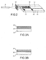
- waveguide coupling It has also been proposed to use waveguide coupling (see [Jackson 03]).
- the light 6 issuing from a monomode optical fiber 8 is focused along a line by a diffractive optical element 10 and injected by the latter into a silicon multi-mode planar waveguide 12 which is formed on a silica substrate 14. It is pointed out that this waveguide is monomode vertical but laterally multimode.
- An NbN coil 16 is deposited on top of this silicon guide. The ends of this coil are respectively provided with contact pads 18 and 20. The coil 16 absorbs the evanescent wave which is associated with the guided mode.
- a photon, which one wants to detect, is likely to be absorbed by a branch of the meanders formed by the coil, with each passage of the evanescent wave.
- the absorption of light energy by the NbN can, in principle, approach 100% if the meanders are sufficiently numerous. But, as a result, the detection efficiency is limited by the large length of NbN.
- FIG. 3A An example of such a structure is schematically represented on the figure 3A where we see a substrate 22 covered with a sapphire layer 24, serving as a waveguide, and a layer of NbN 26 which covers this layer 24.
- the NbN layer is between the substrate and the sapphire layer.
- the length of NbN needed to absorb the light is typically a few tens of microns (the calculations being made in one dimension, for planar guides).
- the present invention aims to solve the problem of the design of an ultrasensitive optical detector, with a high temporal resolution, in particular of an SSPD type detector, this detector having a detection efficiency that is clearly greater than those obtained in the prior art, this detector being capable of operating at normal incidence and being furthermore feasible by existing technological means.
- Operation at normal incidence allows to consider a simple positioning system and reduced space in a cryostat, and the possibility of extending the principle of coupling to a matrix of detectors used for example in imaging.
- the structure of the optical detector which is the subject of the invention, makes it possible to considerably improve the detection efficiency by means of the one-dimensional dielectric network situated above the serpentine-forming detection element.
- the detector object of the invention must be able to operate with a very low photon flux.
- the probability of absorption of a photon is assumed to be proportional to the local intensity of the field that one would have with a large and continuous flow of photons (same maps).
- the incidence given is a normal incidence.
- the superstrate can be a gas, for example air, a liquid, a solid or even a vacuum (in which case neither is 1).
- the step (in English, pitch) A of the one-dimensional dielectric network is less than ⁇ o / n o , where ⁇ o represents the wavelength in the vacuum of the photon or photons, and the pair (w r / ⁇ , d) is chosen to lead to absorption resonance, where w r is the width of the first lines of the one-dimensional dielectric lattice and d is the thickness of this one-dimensional dielectric lattice, and A is furthermore less than ⁇ o / n i .
- n H -n B is preferably greater than 1.
- the detection element is made of a superconducting material.
- This superconducting material may be a superconducting nitride phase.
- This phase may be niobium nitride.
- the coil comprises parallel lines, connected to each other, and each line of the coil is arranged opposite one of the lines of the one-dimensional dielectric network.
- the coil comprises parallel lines, connected to each other, and each line of the coil is disposed opposite one of the first lines of the one-dimensional dielectric network.
- the coil comprises parallel lines, connected to each other, and the lines of the coil and the first lines of the one-dimensional dielectric network have the same width and form periodic sets having the same period.
- the first lines of the one-dimensional dielectric network have different widths W rL and W rS and the first lines whose width is w rL alternate with those whose width is w rS .
- the second lines of the one-dimensional dielectric lattice may also have different widths.
- the optical detector further comprises an intermediate layer which is made of a dielectric material having a refractive index n greater than n B and which is placed between the detection element and the one-dimensional dielectric network.
- the present invention also relates to an optical detector, intended to detect one or more photons, this optical detector comprising a polarization splitter comprising a port , intended to receive the photons, and two output channels which are respectively connected to two optical detectors according to the invention.
- the present invention further relates to a matrix of optical detectors according to the invention.
- the figure 4 is a schematic sectional view of an example of the detector object of the invention. This detector is intended to detect an incident light 28, consisting of a single photon or several photons.
- the structure considered on the figure 4 comprises a dielectric substrate 30, whose refractive index is noted n o , and an ultra-thin superconducting layer 32, for example NbN, whose thickness is a few nanometers, on the dielectric substrate 30.
- the latter is suitable for deposit of the layer 32.
- This layer 32 is intended to generate an electrical signal from the energy of the photon or photons received. It forms a coil and therefore meanders as in the prior art.
- the coil preferably configurations in which the coil covers the largest possible area in the area illuminated by the incident light, so that a maximum of photons is absorbed by the superconductor which is made the coil.
- the detector of the figure 4 also includes a one-dimensional dielectric grating 34, including parallel lines which are formed over the superconducting layer 32 in a high index dielectric material n H. These lines 36 alternate with other lines 38 which are made of a dielectric medium of low index n B. As can be seen, the lines 36 and 38 are parallel to the lines of the layer 32.
- the detector comprises a superstrate 40 whose refractive index is denoted ni. This superstrate is placed above the dielectric network 34.
- the period, or not (in English, pitch ) of the network 34 is denoted by A, the width of the lines of high index W r and the width of the low index lines w g .
- the superconducting lines 44 of the layer 32 are separated by gaps 46 which are made of a dielectric material whose refractive index is denoted n F.
- the operating principle of the detector of the figure 4 is based on the excitation of an absorption resonance of the incident light 28 in the segmented guide constituted by the grating 34 (see below), for a given polarization and wavelength, for example a TE polarization, incident light 28 (the direction of polarization then being parallel to the lines of the network 34).
- the incident light 28 is partially reflected in the superstrate 40, partially transmitted in the substrate 30, and partially diffracted by the segmented guide constituted by the grating 34.
- the guided light is then partially re-diffracted in the superstrate 40 and in the substrate 30.
- phase shift in English, phaseshift
- ⁇ see [Rosenblatt 97]
- the two waves For a certain wavelength in the vacuum (in English, vacuum) ⁇ 0 of the incident light 28 and a certain orientation of this incident light with respect to the direction of the lines of the grating, the two waves have the same amplitude and the Destructive interference is complete. The transmission is zero and all the incident light is reflected. The described structure is then a resonant structure in reflection (see [Nevière 73]).
- the figure 5 schematically illustrates the waves which are involved in a grating 34 which has a resonance in reflection, as in the example which has been described above.
- the incident light 28 is still seen (normal incidence in the example shown) and the references 48, 50, 52, 54 and 56 respectively represent the directly reflected light, the light guided by the segmented guide, the light directly transmitted, the light guided by the segmented guide then radiated into the superstrate and the light guided by the segmented guide and then radiated into the substrate.
- the letter ⁇ symbolizes the fact that the light directly transmitted in the substrate and the light coupled and then re-diffracted in the substrate interfere destructively.
- the angular acceptance of the device is also much wider and allows to couple a focused beam. Finally, the tolerance on the thickness of the network is substantially increased.
- the superstrate can be simply constituted by air (nor being then equal to 1).
- the lines 38 of the network 34 may be air.
- a strong index contrast is preferably used, which is typically such that the difference n H -n B is greater than 1.
- the structured and very thin superconducting layer disturbs the resonance by absorbing part of the light.
- the transmission is no longer rigorously zero at resonance but remains weak, and the reflection can decrease substantially.
- 80% of the incident light can be absorbed.
- the absorption can be optimized by slightly modifying the geometry of the network 34, as regards its filling factor and its thickness.
- the RCWA method was also used to calculate the reflection, transmission and absorption spectra of the structure of the figure 4 as a function of the wavelength, as well as the evolution of the absoption of this structure as a function of the angle of incidence of the light.
- the width ⁇ FWHM of the wavelength resonance is equal to 60 nm. It is relatively wide and therefore convenient for use.
- the angular width ⁇ FWHM of the resonance is equal to 23 °. It is largely sufficient to effectively couple a light beam whose diameter is 10 .mu.m and which is derived from an optical fiber.
- the maximum absorption of 78% is reached when the lines of the network are centered on NbN lines of the coil. Otherwise, the absorption can drop by about 20%.
- the network makes it possible to concentrate the light preferentially under the lines of the network, and the absorption is maximum if the NbN is located on the lobes of the optical electric field.
- the period of the lobes of the optical electric field is equal to the period of the grating, one can suppress the lines of NbN which are situated under the intervals of low index, where the field is very weak.
- the FDTD simulations then give an absorption of 82% for a resonance length of 1560nm.
- This solution has the merit of halving the necessary length of NbN, and thus of reducing the noise caused by quantum or classical fluctuations, as well as the non-uniformities of width of the superconducting line.
- a uniform thin layer of a dielectric material having a refractive index of n F , may be added above the NbN coil (for technological reasons) without altering the absorption.
- the same period and the same line width are used for the NbN network and the high index network.
- the structure is simpler to realize because it makes it possible to use only one level of photolithography and to carry out an engraving simultaneous, but the precision required on the dimensions is a little more important.
- a high-index uniform dielectric layer 60 is added between the superconducting layer 44 and the grating 34.
- the thickness of the layer 60 is denoted d WG ; its refractive index n I is greater than n B , ni, and n o , preferably n I -n B >1; n I is for example equal to n H.
- the grating 34 the thickness of which is equal to G , only ensures the coupling of the light towards the guide formed by the uniform layer 60.
- This latter structure also has the advantage of being very insensitive to the filling factor of the network 34.
- the absorption of the optical detector object of the invention can be further increased by using an "asymmetric" network instead of a symmetrical network.
- FIG. 7 An example of a detector comprising an asymmetric network is schematically represented on the figure 7 where the network 32 of the figure 6 is replaced by an asymmetric grating 62 in which lines 64, having a width w rL alternate with lines 66 having a width w rs different from w rL .
- the lines 64 and 66 are still made of the dielectric material having the refractive index n H.
- period A of the network 34 is equal to w r + w g in the example of the figure 4 and to w rL + w rs + 2w g in the example of the figure 7 .
- the detector comprises the high index uniform layer 60 and the asymmetrical profile network 62, which is then between the layer 60 and the superstrate 40.
- the propagation distance of the guided wave is very short.
- the light remains confined laterally in an area substantially equal to the size of the beam formed by the incident light. This was verified by FDTD simulation for a Gaussian beam with a diameter of 10 ⁇ m.
- widths W g of the lines 38 of the grating 34 may also be unequal (as may the widths w r of the lines 36). This is of interest: one can have the case where the network consists of a repeating pattern of alternating lines 36 and 38, this pattern comprising several unequally separated lines.
- the materials used in the invention preferably have a very low extinction coefficient, of less than 5 ⁇ 10 -4 , which makes negligible the absorption losses in these materials.
- the detectors according to the invention are designed for a given polarization (TE or TM) of the incident light.
- TE or TM polarization of the incident light
- FIG. 9 This is schematically illustrated by the figure 9 where we see a polarization separator 68 whose input channel 70 receives the light to be detected 72 and whose two output channels 74 and 76 are respectively coupled to two detectors according to the invention 78 and 80 to inject therein respectively a polarized beam TE and a polarized beam TM, resulting from the decomposition of the light 72 by the separator 68.
- optical detector object of the invention
- typical dimensions are 10 ⁇ 10 ⁇ m and which is illuminated by a focused light beam, for example from an optical fiber of the same diameter. (10 .mu.m).
- the principle of the invention can be extended to the design of a matrix of pixels that is illuminated by a larger light beam, for example for ultrasensitive imaging applications, in which case the angular width criterion can to be relaxed.
- Such a detector is achievable by well controlled technological means (deposition of thin layers, transfer of substrates).
- the thicknesses of the layers are not critical (tolerance of the order of ⁇ 5%), except for the thickness of the superconducting layer, which is known to be well controlled by epitaxy.
- the size of the sapphire substrates may be selected to be compatible with that of the silicon substrates that are used in the microelectronic industry (100 or 200mm). This makes it possible to produce many chips at a low cost on the same substrate.
- the manufacturing method that has just been described also comprises a step of depositing an amorphous or polycrystalline Si layer (n H and n F being equal and taking a value of 3 to 3.5) on the coil , before the formation of the network, the latter then being formed on the amorphous or polycrystalline Si layer thus deposited.
- the structure proposed in the present invention is achievable by well-controlled technological means (deposition of thin layers, transfer of substrates).
- the thicknesses of the layers are not critical (tolerance of the order of + 5%), except that of the superconductor, which is known to be well controlled by epitaxy.
- the indicated methods can be applied to the realization of a detector comprising a single pixel or a matrix of detectors.
- NbN instead of NbN, other superconductive materials can be used to form the detection element, for example other nitride phases (for example MoN or TiN) or cuprate phases (for example YBa 2 Cu 3 O 7 -x or ReBa 2 Cu 3 O 7-x ).
- nitride phases for example MoN or TiN
- cuprate phases for example YBa 2 Cu 3 O 7 -x or ReBa 2 Cu 3 O 7-x .
- this detection element can be made of any material able to detect a low light energy and to restore an electrical signal corresponding to this energy.
- This can be for example a semiconductor or bolometric material.
- the superstrate is air but it can be another gas (all gases have a refractive index close to 1) or a liquid, for example liquid helium (whose refractive index is 1.025) or a solid, for example silica (whose refractive index is 1.45 in the visible and near-infrared ranges), or even vacuum , in which case the refractive index is 1 and then work under vacuum.
- gases have a refractive index close to 1
- a liquid for example liquid helium (whose refractive index is 1.025) or a solid, for example silica (whose refractive index is 1.45 in the visible and near-infrared ranges), or even vacuum , in which case the refractive index is 1 and then work under vacuum.
Landscapes
- Physics & Mathematics (AREA)
- General Physics & Mathematics (AREA)
- Spectroscopy & Molecular Physics (AREA)
- Photometry And Measurement Of Optical Pulse Characteristics (AREA)
- Superconductor Devices And Manufacturing Methods Thereof (AREA)
- Investigating Or Analysing Materials By Optical Means (AREA)
- Holo Graphy (AREA)
- Measurement Of The Respiration, Hearing Ability, Form, And Blood Characteristics Of Living Organisms (AREA)
Claims (14)
- Optischer Detektor, bestimmt zur Detektion wenigstens eines Photons, wobei dieser Detektor umfasst:- ein dielektrisches Substrat (30) mit einer Brechzahl nO, und- ein auf dem dielektrischen Substrat ausgebildetes, die Form einer Schlange aufweisendes Detektionselement (32), dazu bestimmt, aus der Energie des empfangenen Photons oder der empfangenen Photonen ein elektrisches Signal zu erzeugen,wobei dieser optische Detektor dadurch gekennzeichnet ist,
dass er außerdem umfasst:- ein eindimensionales dielektrisches Gitter (34, 62) mit parallelen Linien, nämlich ersten Linien (36, 64, 66), die aus einem ersten dielektrischen Material mit einer Brechzahl nH sind, und zweiten Linien (38), die sich mit den ersten Linien abwechseln und aus einem zweiten dielektrischen Material mit einer Brechzahl nB sind, wobei sich das eindimensionale dielektrische Gitter über dem Detektionselement befindet und das durch das eindimensionale dielektrische Gitter und das Detektionselement gebildete Ganze dabei unter einem gegebenen Einfallswinkel und bei einer gegebenen Polarisation des Photons oder der Photonen eine Absorptionsresonanz dieses Photons oder dieser Photonen aufweist, wobei nH größer ist als nO und als nB, und- ein Substrat (40) mit einer Brechzahl ni, wobei dieses Substrat sich über dem eindimensionalen dielektrischen Gitter befindet und nH zudem größer als ni ist. - Optischer Detektor nach Anspruch 1, bei dem der gegebene Einfallwinkel ein normaler Einfallswinkel ist.
- Optischer Detektor nach einem der Ansprüche 1 und 2, bei dem das Substrat ein Gas, insbesondere Luft, eine Flüssigkeit, ein Feststoff oder Vakuum ist.
- Optischer Detektor nach einem der Ansprüche 1 bis 3, bei dem die Teilung Λ des eindimensionalen dielektrischen Gitters (34) kleiner ist als λO/nO, wo λO die Wellenlänge des Photons oder der Photonen im Vakuum darstellt, und das Paar (wr/Λ, d) ausgewählt wird, um zur Absorptionsresonanz zu führen, wo wr die Breite der ersten Linien (36) des eindimensionalen dielektrischen Gitters darstellt, d die Dicke dieses eindimensionalen dielektrischen Gitters (34) darstellt und Λ zudem kleiner als λO/ni ist.
- Optischer Detektor nach einem der Ansprüche 1 bis 4, bei dem die Differenz nH-nB größer als 1 ist.
- Optischer Detektor nach einem der Ansprüche 1 bis 5, bei dem das Detektionselement (32) aus einem supraleitenden Material ist.
- Optischer Detektor nach einem der Ansprüche 1 bis 6, bei dem die Schlange miteinander verbundene parallele Linien (44) umfasst und jede Linie (44) der Schlange einer der Linien (36, 38) des eindimensionalen dielektrischen Gitters gegenübersteht.
- Optischer Detektor nach einem der Ansprüche 1 bis 6, bei dem die Schlange miteinander verbundene parallele Linien (44) umfasst und jede Linie (44) der Schlange einer der ersten Linien (36) des eindimensionalen dielektrischen Gitters gegenübersteht.
- Optischer Detektor nach einem der Ansprüche 1 bis 8, bei dem die Schlange miteinander verbundene parallele Linien (44) umfasst und die Linien (44) der Schlange und die ersten Linien (36) des eindimensionalen dielektrischen Gitters die gleiche Breite haben und periodische Gruppen bilden, welche die gleiche Periode haben.
- Optischer Detektor nach einem der Ansprüche 1 bis 3 und 5 bis 8, bei dem die ersten Linien (64, 66) des eindimensionalen dielektrischen Gitters (62) unterschiedliche Breiten wrL und wrS haben, und die ersten Linien (64), deren Breite wrL beträgt, sich mit den ersten Linien (66) abwechseln, deren Breite wrS beträgt.
- Optischer Detektor nach einem der Ansprüche 1 bis 10, bei dem die zweiten Linien (38) des eindimensionalen dielektrischen Gitters unterschiedliche Breiten haben.
- Optischer Detektor nach einem der Ansprüche 1 bis 11, der zudem eine Zwischenschicht (60) umfasst, die aus einem dielektrischen Material mit einer Brechzahl n größer als nB ist und die sich zwischen dem Detektionselement (32) und dem eindimensionalen dielektrischen Gitter (34) befindet.
- Optischer Detektor, bestimmt zur Detektion von einem Photon oder von Photonen, wobei dieser optische Detektor umfasst: einen Polarisationsseparator (68) mit einem Eingangskanal (70), dazu bestimmt, das Photon oder die Photonen zu empfangen, und zwei Ausgangskanäle (74, 76), jeweils verbunden mit zwei optischen Detektoren (78, 80) nach einem der vorangehenden Ansprüche 1 bis 12.
- Optischer Detektor mit einer Matrix aus optischen Detektoren nach einem der Ansprüche 1 bis 13.
Applications Claiming Priority (1)
| Application Number | Priority Date | Filing Date | Title |
|---|---|---|---|
| FR0654109A FR2906934B1 (fr) | 2006-10-05 | 2006-10-05 | Detecteur optique ultrasensible a grande resolution temporelle, utilisant un couplage a reseau. |
Publications (2)
| Publication Number | Publication Date |
|---|---|
| EP1909080A1 EP1909080A1 (de) | 2008-04-09 |
| EP1909080B1 true EP1909080B1 (de) | 2009-05-06 |
Family
ID=37964091
Family Applications (1)
| Application Number | Title | Priority Date | Filing Date |
|---|---|---|---|
| EP07117593A Not-in-force EP1909080B1 (de) | 2006-10-05 | 2007-10-01 | Ultrasensibler optischer Detektor mit hoher zeitlicher Auflösung basierend auf einem Gitter. |
Country Status (5)
| Country | Link |
|---|---|
| US (1) | US7763854B2 (de) |
| EP (1) | EP1909080B1 (de) |
| AT (1) | ATE430922T1 (de) |
| DE (1) | DE602007001062D1 (de) |
| FR (1) | FR2906934B1 (de) |
Families Citing this family (29)
| Publication number | Priority date | Publication date | Assignee | Title |
|---|---|---|---|---|
| US7615385B2 (en) | 2006-09-20 | 2009-11-10 | Hypres, Inc | Double-masking technique for increasing fabrication yield in superconducting electronics |
| US20100252744A1 (en) * | 2009-04-06 | 2010-10-07 | Koninklijke Philips Electronics N.V. | Radiation detector with a plurality of electrode systems |
| WO2011150321A1 (en) | 2010-05-28 | 2011-12-01 | Massachusetts Institute Of Technology | Photon detector based on superconducting nanowires |
| US10268843B2 (en) | 2011-12-06 | 2019-04-23 | AEMEA Inc. | Non-deterministic secure active element machine |
| CN102353464B (zh) * | 2011-07-14 | 2012-11-14 | 清华大学 | 一种能分辨光子数的超导纳米线单光子探测器及制备方法 |
| US9076907B2 (en) | 2011-10-06 | 2015-07-07 | Massachusetts Institute Of Technology | Compactly-integrated optical detectors and associated systems and methods |
| US9726536B2 (en) * | 2011-12-23 | 2017-08-08 | Technion Research And Development Foundation Limited | Fiber optical superconducting nanowire single photon detector |
| FR2985604B1 (fr) * | 2012-01-06 | 2014-03-14 | Commissariat Energie Atomique | Dispositif de photodetection. |
| US9235697B2 (en) | 2012-03-05 | 2016-01-12 | Biogy, Inc. | One-time passcodes with asymmetric keys |
| CN102661801B (zh) * | 2012-06-06 | 2013-12-25 | 华中科技大学 | 一种超分辨率红外热像仪及用其获取高分辨率红外图像的方法 |
| CN103165723B (zh) * | 2013-03-26 | 2015-07-29 | 中国科学院上海技术物理研究所 | 一种汇聚增强光响应超导单光子探测器及其制备方法 |
| US9806217B2 (en) * | 2014-04-30 | 2017-10-31 | William Marsh Rice University | Fully integrated CMOS-compatible photodetector with color selectivity and intrinsic gain |
| CN104167452B (zh) * | 2014-08-12 | 2016-03-30 | 南京大学 | 一种带相位光栅的超导单光子探测器及其制备方法 |
| US10205081B2 (en) | 2014-11-20 | 2019-02-12 | The Regents Of The University Of California | Magnetic flux-to-voltage transducer based on josephson junction arrays |
| JP2016148534A (ja) * | 2015-02-10 | 2016-08-18 | 国立研究開発法人情報通信研究機構 | 蛍光相関分光装置 |
| US9490112B2 (en) * | 2015-03-06 | 2016-11-08 | Robert Francis McDermott, III | System and method for characterizing ions using a superconducting transmission line detector |
| CN106558632B (zh) * | 2015-09-17 | 2018-04-03 | 中国科学院上海微系统与信息技术研究所 | 高偏振消光比超导纳米线单光子探测器 |
| CN106549099B (zh) * | 2015-09-17 | 2019-02-01 | 中国科学院上海微系统与信息技术研究所 | 基于深硅刻蚀工艺的超导纳米线单光子探测器及制备方法 |
| CN106549097B (zh) * | 2015-09-17 | 2019-05-10 | 中国科学院上海微系统与信息技术研究所 | 抑制偏振敏感度的超导纳米线单光子探测器 |
| US10785625B2 (en) * | 2016-02-17 | 2020-09-22 | Wistron Aidge Corporation | Internet of Things (IOT) companion device |
| KR102616213B1 (ko) * | 2017-09-13 | 2023-12-21 | 구글 엘엘씨 | 초전도 양자 컴퓨팅을 위한 하이브리드 키네틱 인덕턴스 장치 |
| EP3871261A4 (de) | 2018-10-26 | 2022-08-03 | Psiquantum, Corp. | Isolation von wellenleiterintegrierten detektoren unter verwendung eines backend-of-line-verfahrens |
| US11193914B2 (en) * | 2019-01-29 | 2021-12-07 | Government Of The United States Of America, As Represented By The Secretary Of Commerce | Photoacoustic photon meter and process for measuring photon fluence |
| CN110890434B (zh) * | 2019-10-31 | 2021-05-25 | 山东大学 | 一种铜氧基高温超导单光子探测器及其制备方法 |
| TWI780579B (zh) * | 2020-02-03 | 2022-10-11 | 美商應用材料股份有限公司 | 具有整合化氮化鋁晶種或波導層的超導奈米線單光子偵測器 |
| TW202229949A (zh) | 2020-09-28 | 2022-08-01 | 美商匹西量子股份有限公司 | 用以結合多個低損耗光子電路元件的方法及構造 |
| US12048256B2 (en) * | 2021-04-27 | 2024-07-23 | Microsoft Technology Licensing, Llc | Interfacing with superconducting circuitry |
| US12306040B2 (en) * | 2021-07-23 | 2025-05-20 | Photonic Inc. | Superconducting single photon detector with photon number resolution |
| US12029141B1 (en) * | 2021-08-30 | 2024-07-02 | National Technology & Engineering Solutions Of Sandia, Llc | Systems and methods for resolving a number of incident RF-range photons |
Family Cites Families (10)
| Publication number | Priority date | Publication date | Assignee | Title |
|---|---|---|---|---|
| US5619369A (en) * | 1992-07-16 | 1997-04-08 | Matsushita Electric Industrial Co., Ltd. | Diffracting device having distributed bragg reflector and wavelength changing device having optical waveguide with periodically inverted-polarization layers |
| US5532485A (en) * | 1994-10-14 | 1996-07-02 | Northrop Grumman Corp. | Multispectral superconductive quantum detector |
| US5925878A (en) * | 1997-08-20 | 1999-07-20 | Imation Corp. | Diffraction anomaly sensor having grating coated with protective dielectric layer |
| US5907427A (en) * | 1997-10-24 | 1999-05-25 | Time Domain Corporation | Photonic band gap device and method using a periodicity defect region to increase photonic signal delay |
| US6812464B1 (en) * | 2000-07-28 | 2004-11-02 | Credence Systems Corporation | Superconducting single photon detector |
| US7575939B2 (en) * | 2000-10-30 | 2009-08-18 | Sru Biosystems, Inc. | Optical detection of label-free biomolecular interactions using microreplicated plastic sensor elements |
| US7142296B2 (en) * | 2000-10-30 | 2006-11-28 | Sru Biosystems, Inc. | Method and apparatus for detecting biomolecular interactions |
| US6816648B2 (en) * | 2002-05-01 | 2004-11-09 | Intel Corporation | Integrated waveguide gratings by ion implantation |
| US6998613B2 (en) * | 2003-04-22 | 2006-02-14 | Raytheon Company | Integrated spectroscopic microbolometer with microfilter arrays |
| US7969422B2 (en) * | 2005-07-15 | 2011-06-28 | Avago Technologies General Ip (Singapore) Pte. Ltd. | Pattern detection system |
-
2006
- 2006-10-05 FR FR0654109A patent/FR2906934B1/fr not_active Expired - Fee Related
-
2007
- 2007-09-26 US US11/861,876 patent/US7763854B2/en not_active Expired - Fee Related
- 2007-10-01 AT AT07117593T patent/ATE430922T1/de not_active IP Right Cessation
- 2007-10-01 DE DE602007001062T patent/DE602007001062D1/de active Active
- 2007-10-01 EP EP07117593A patent/EP1909080B1/de not_active Not-in-force
Also Published As
| Publication number | Publication date |
|---|---|
| US20090020701A1 (en) | 2009-01-22 |
| DE602007001062D1 (de) | 2009-06-18 |
| ATE430922T1 (de) | 2009-05-15 |
| FR2906934A1 (fr) | 2008-04-11 |
| EP1909080A1 (de) | 2008-04-09 |
| FR2906934B1 (fr) | 2009-01-30 |
| US7763854B2 (en) | 2010-07-27 |
Similar Documents
| Publication | Publication Date | Title |
|---|---|---|
| EP1909080B1 (de) | Ultrasensibler optischer Detektor mit hoher zeitlicher Auflösung basierend auf einem Gitter. | |
| EP1891677A2 (de) | Hochempfindlicher, einen wellenleiter verwendender optischer detektor mit hoher zeitauflösung und herstellungsverfahren dafür | |
| WO2006114540A2 (fr) | Detecteur optique ultrasensible a grande resolution temporelle | |
| EP1929539B1 (de) | Einen planarwellenleiter-leckmodus verwendender zeitlich hoch auflösender ultraempfindlicher optischer sensor und herstellungsverfahren dafür | |
| EP3190672B1 (de) | Laserquelle mit halbleiter | |
| EP2450681B1 (de) | Infrarotdetektor auf der Basis von hängenden bolometrischen Mikroplatten | |
| CN107532967B (zh) | 用于测试光学器件性能的系统和测试光学装置的方法 | |
| EP0033048B1 (de) | Interferometer mit abstimmbarer optischer Höhlung, das eine optische monomoden Faser befasst, und dessen Anwendung zur Filtrierung und Spektrographie | |
| EP1461650A2 (de) | Photonische kristallstruktur zur modenumwandlung | |
| FR2966643A1 (fr) | Dispositif de detection de photon assiste par plasmons de surface et procede de fabrication du dispositif | |
| FR2855609A1 (fr) | Dispositif de detection bolometrique a antenne, a cavite optimisee, pour ondes electromagnetiques millimetriques ou submillimetriques, et procede de fabrication de ce dispositif | |
| Baek et al. | Superconducting nanowire single-photon detector in an optical cavity for front-side illumination | |
| EP2652793A2 (de) | Fotodetektor | |
| EP2801115B1 (de) | Fotodetektor | |
| EP1752803B1 (de) | Integrierte optoelektronische Vorrichtung | |
| EP1516212A2 (de) | Optischer wellenlängenselektiver richtkoppler | |
| EP3968066B1 (de) | Wellenleiter, der eine optische multimode-faser umfasst und die geführten moden räumlich konzentrieren kann | |
| FR3065323B1 (fr) | Photodiode | |
| FR2748604A1 (fr) | Photodetecteur a structure optique resonnante avec un reseau | |
| WO2025099171A1 (fr) | Circuit photonique pour la détection de photons uniques | |
| EP0198735A1 (de) | Optoelektronischer Wandler und Verfahren zu seiner Herstellung | |
| Casalino et al. | Microcavity silicon photodetectors at 1.55 μm |
Legal Events
| Date | Code | Title | Description |
|---|---|---|---|
| PUAI | Public reference made under article 153(3) epc to a published international application that has entered the european phase |
Free format text: ORIGINAL CODE: 0009012 |
|
| AK | Designated contracting states |
Kind code of ref document: A1 Designated state(s): AT BE BG CH CY CZ DE DK EE ES FI FR GB GR HU IE IS IT LI LT LU LV MC MT NL PL PT RO SE SI SK TR |
|
| AX | Request for extension of the european patent |
Extension state: AL BA HR MK RS |
|
| GRAP | Despatch of communication of intention to grant a patent |
Free format text: ORIGINAL CODE: EPIDOSNIGR1 |
|
| 17P | Request for examination filed |
Effective date: 20080929 |
|
| GRAJ | Information related to disapproval of communication of intention to grant by the applicant or resumption of examination proceedings by the epo deleted |
Free format text: ORIGINAL CODE: EPIDOSDIGR1 |
|
| GRAP | Despatch of communication of intention to grant a patent |
Free format text: ORIGINAL CODE: EPIDOSNIGR1 |
|
| AKX | Designation fees paid |
Designated state(s): AT BE BG CH CY CZ DE DK EE ES FI FR GB GR HU IE IS IT LI LT LU LV MC MT NL PL PT RO SE SI SK TR |
|
| RAP1 | Party data changed (applicant data changed or rights of an application transferred) |
Owner name: COMMISSARIAT A L'ENERGIE ATOMIQUE |
|
| GRAS | Grant fee paid |
Free format text: ORIGINAL CODE: EPIDOSNIGR3 |
|
| GRAA | (expected) grant |
Free format text: ORIGINAL CODE: 0009210 |
|
| AK | Designated contracting states |
Kind code of ref document: B1 Designated state(s): AT BE BG CH CY CZ DE DK EE ES FI FR GB GR HU IE IS IT LI LT LU LV MC MT NL PL PT RO SE SI SK TR |
|
| REG | Reference to a national code |
Ref country code: GB Ref legal event code: FG4D Free format text: NOT ENGLISH |
|
| REG | Reference to a national code |
Ref country code: CH Ref legal event code: EP |
|
| REG | Reference to a national code |
Ref country code: IE Ref legal event code: FG4D |
|
| REF | Corresponds to: |
Ref document number: 602007001062 Country of ref document: DE Date of ref document: 20090618 Kind code of ref document: P |
|
| PG25 | Lapsed in a contracting state [announced via postgrant information from national office to epo] |
Ref country code: AT Free format text: LAPSE BECAUSE OF FAILURE TO SUBMIT A TRANSLATION OF THE DESCRIPTION OR TO PAY THE FEE WITHIN THE PRESCRIBED TIME-LIMIT Effective date: 20090506 Ref country code: PT Free format text: LAPSE BECAUSE OF FAILURE TO SUBMIT A TRANSLATION OF THE DESCRIPTION OR TO PAY THE FEE WITHIN THE PRESCRIBED TIME-LIMIT Effective date: 20090906 Ref country code: LT Free format text: LAPSE BECAUSE OF FAILURE TO SUBMIT A TRANSLATION OF THE DESCRIPTION OR TO PAY THE FEE WITHIN THE PRESCRIBED TIME-LIMIT Effective date: 20090506 Ref country code: FI Free format text: LAPSE BECAUSE OF FAILURE TO SUBMIT A TRANSLATION OF THE DESCRIPTION OR TO PAY THE FEE WITHIN THE PRESCRIBED TIME-LIMIT Effective date: 20090506 Ref country code: ES Free format text: LAPSE BECAUSE OF FAILURE TO SUBMIT A TRANSLATION OF THE DESCRIPTION OR TO PAY THE FEE WITHIN THE PRESCRIBED TIME-LIMIT Effective date: 20090817 |
|
| NLV1 | Nl: lapsed or annulled due to failure to fulfill the requirements of art. 29p and 29m of the patents act | ||
| PG25 | Lapsed in a contracting state [announced via postgrant information from national office to epo] |
Ref country code: SI Free format text: LAPSE BECAUSE OF FAILURE TO SUBMIT A TRANSLATION OF THE DESCRIPTION OR TO PAY THE FEE WITHIN THE PRESCRIBED TIME-LIMIT Effective date: 20090506 Ref country code: SE Free format text: LAPSE BECAUSE OF FAILURE TO SUBMIT A TRANSLATION OF THE DESCRIPTION OR TO PAY THE FEE WITHIN THE PRESCRIBED TIME-LIMIT Effective date: 20090806 Ref country code: IS Free format text: LAPSE BECAUSE OF FAILURE TO SUBMIT A TRANSLATION OF THE DESCRIPTION OR TO PAY THE FEE WITHIN THE PRESCRIBED TIME-LIMIT Effective date: 20090906 Ref country code: LV Free format text: LAPSE BECAUSE OF FAILURE TO SUBMIT A TRANSLATION OF THE DESCRIPTION OR TO PAY THE FEE WITHIN THE PRESCRIBED TIME-LIMIT Effective date: 20090506 Ref country code: PL Free format text: LAPSE BECAUSE OF FAILURE TO SUBMIT A TRANSLATION OF THE DESCRIPTION OR TO PAY THE FEE WITHIN THE PRESCRIBED TIME-LIMIT Effective date: 20090506 Ref country code: NL Free format text: LAPSE BECAUSE OF FAILURE TO SUBMIT A TRANSLATION OF THE DESCRIPTION OR TO PAY THE FEE WITHIN THE PRESCRIBED TIME-LIMIT Effective date: 20090506 |
|
| REG | Reference to a national code |
Ref country code: IE Ref legal event code: FD4D |
|
| PG25 | Lapsed in a contracting state [announced via postgrant information from national office to epo] |
Ref country code: IE Free format text: LAPSE BECAUSE OF FAILURE TO SUBMIT A TRANSLATION OF THE DESCRIPTION OR TO PAY THE FEE WITHIN THE PRESCRIBED TIME-LIMIT Effective date: 20090506 Ref country code: RO Free format text: LAPSE BECAUSE OF FAILURE TO SUBMIT A TRANSLATION OF THE DESCRIPTION OR TO PAY THE FEE WITHIN THE PRESCRIBED TIME-LIMIT Effective date: 20090506 Ref country code: DK Free format text: LAPSE BECAUSE OF FAILURE TO SUBMIT A TRANSLATION OF THE DESCRIPTION OR TO PAY THE FEE WITHIN THE PRESCRIBED TIME-LIMIT Effective date: 20090506 Ref country code: EE Free format text: LAPSE BECAUSE OF FAILURE TO SUBMIT A TRANSLATION OF THE DESCRIPTION OR TO PAY THE FEE WITHIN THE PRESCRIBED TIME-LIMIT Effective date: 20090506 Ref country code: CZ Free format text: LAPSE BECAUSE OF FAILURE TO SUBMIT A TRANSLATION OF THE DESCRIPTION OR TO PAY THE FEE WITHIN THE PRESCRIBED TIME-LIMIT Effective date: 20090506 |
|
| PG25 | Lapsed in a contracting state [announced via postgrant information from national office to epo] |
Ref country code: SK Free format text: LAPSE BECAUSE OF FAILURE TO SUBMIT A TRANSLATION OF THE DESCRIPTION OR TO PAY THE FEE WITHIN THE PRESCRIBED TIME-LIMIT Effective date: 20090506 |
|
| PLBE | No opposition filed within time limit |
Free format text: ORIGINAL CODE: 0009261 |
|
| STAA | Information on the status of an ep patent application or granted ep patent |
Free format text: STATUS: NO OPPOSITION FILED WITHIN TIME LIMIT |
|
| PG25 | Lapsed in a contracting state [announced via postgrant information from national office to epo] |
Ref country code: BG Free format text: LAPSE BECAUSE OF FAILURE TO SUBMIT A TRANSLATION OF THE DESCRIPTION OR TO PAY THE FEE WITHIN THE PRESCRIBED TIME-LIMIT Effective date: 20090806 |
|
| 26N | No opposition filed |
Effective date: 20100209 |
|
| BERE | Be: lapsed |
Owner name: COMMISSARIAT A L'ENERGIE ATOMIQUE Effective date: 20091031 |
|
| PG25 | Lapsed in a contracting state [announced via postgrant information from national office to epo] |
Ref country code: MC Free format text: LAPSE BECAUSE OF NON-PAYMENT OF DUE FEES Effective date: 20091031 |
|
| PG25 | Lapsed in a contracting state [announced via postgrant information from national office to epo] |
Ref country code: BE Free format text: LAPSE BECAUSE OF NON-PAYMENT OF DUE FEES Effective date: 20091031 Ref country code: GR Free format text: LAPSE BECAUSE OF FAILURE TO SUBMIT A TRANSLATION OF THE DESCRIPTION OR TO PAY THE FEE WITHIN THE PRESCRIBED TIME-LIMIT Effective date: 20090807 |
|
| PG25 | Lapsed in a contracting state [announced via postgrant information from national office to epo] |
Ref country code: MT Free format text: LAPSE BECAUSE OF FAILURE TO SUBMIT A TRANSLATION OF THE DESCRIPTION OR TO PAY THE FEE WITHIN THE PRESCRIBED TIME-LIMIT Effective date: 20090506 Ref country code: LU Free format text: LAPSE BECAUSE OF NON-PAYMENT OF DUE FEES Effective date: 20091001 |
|
| PG25 | Lapsed in a contracting state [announced via postgrant information from national office to epo] |
Ref country code: HU Free format text: LAPSE BECAUSE OF FAILURE TO SUBMIT A TRANSLATION OF THE DESCRIPTION OR TO PAY THE FEE WITHIN THE PRESCRIBED TIME-LIMIT Effective date: 20091107 |
|
| PG25 | Lapsed in a contracting state [announced via postgrant information from national office to epo] |
Ref country code: TR Free format text: LAPSE BECAUSE OF FAILURE TO SUBMIT A TRANSLATION OF THE DESCRIPTION OR TO PAY THE FEE WITHIN THE PRESCRIBED TIME-LIMIT Effective date: 20090506 |
|
| PG25 | Lapsed in a contracting state [announced via postgrant information from national office to epo] |
Ref country code: CY Free format text: LAPSE BECAUSE OF FAILURE TO SUBMIT A TRANSLATION OF THE DESCRIPTION OR TO PAY THE FEE WITHIN THE PRESCRIBED TIME-LIMIT Effective date: 20090506 |
|
| PG25 | Lapsed in a contracting state [announced via postgrant information from national office to epo] |
Ref country code: IT Free format text: LAPSE BECAUSE OF NON-PAYMENT OF DUE FEES Effective date: 20101001 |
|
| REG | Reference to a national code |
Ref country code: CH Ref legal event code: PL |
|
| PG25 | Lapsed in a contracting state [announced via postgrant information from national office to epo] |
Ref country code: CH Free format text: LAPSE BECAUSE OF NON-PAYMENT OF DUE FEES Effective date: 20111031 Ref country code: LI Free format text: LAPSE BECAUSE OF NON-PAYMENT OF DUE FEES Effective date: 20111031 |
|
| REG | Reference to a national code |
Ref country code: FR Ref legal event code: PLFP Year of fee payment: 9 |
|
| PGFP | Annual fee paid to national office [announced via postgrant information from national office to epo] |
Ref country code: DE Payment date: 20151014 Year of fee payment: 9 Ref country code: IT Payment date: 20151014 Year of fee payment: 9 Ref country code: GB Payment date: 20151019 Year of fee payment: 9 |
|
| PGFP | Annual fee paid to national office [announced via postgrant information from national office to epo] |
Ref country code: FR Payment date: 20151102 Year of fee payment: 9 |
|
| REG | Reference to a national code |
Ref country code: DE Ref legal event code: R119 Ref document number: 602007001062 Country of ref document: DE |
|
| GBPC | Gb: european patent ceased through non-payment of renewal fee |
Effective date: 20161001 |
|
| REG | Reference to a national code |
Ref country code: FR Ref legal event code: ST Effective date: 20170630 |
|
| PG25 | Lapsed in a contracting state [announced via postgrant information from national office to epo] |
Ref country code: DE Free format text: LAPSE BECAUSE OF NON-PAYMENT OF DUE FEES Effective date: 20170503 Ref country code: FR Free format text: LAPSE BECAUSE OF NON-PAYMENT OF DUE FEES Effective date: 20161102 Ref country code: GB Free format text: LAPSE BECAUSE OF NON-PAYMENT OF DUE FEES Effective date: 20161001 |
|
| PG25 | Lapsed in a contracting state [announced via postgrant information from national office to epo] |
Ref country code: IT Free format text: LAPSE BECAUSE OF NON-PAYMENT OF DUE FEES Effective date: 20161001 |