EP1908527A1 - Electrostatic atomizer - Google Patents
Electrostatic atomizer Download PDFInfo
- Publication number
- EP1908527A1 EP1908527A1 EP06768257A EP06768257A EP1908527A1 EP 1908527 A1 EP1908527 A1 EP 1908527A1 EP 06768257 A EP06768257 A EP 06768257A EP 06768257 A EP06768257 A EP 06768257A EP 1908527 A1 EP1908527 A1 EP 1908527A1
- Authority
- EP
- European Patent Office
- Prior art keywords
- voltage
- current
- discharge
- transistor
- detector
- Prior art date
- Legal status (The legal status is an assumption and is not a legal conclusion. Google has not performed a legal analysis and makes no representation as to the accuracy of the status listed.)
- Granted
Links
Images


Classifications
-
- B—PERFORMING OPERATIONS; TRANSPORTING
- B05—SPRAYING OR ATOMISING IN GENERAL; APPLYING FLUENT MATERIALS TO SURFACES, IN GENERAL
- B05B—SPRAYING APPARATUS; ATOMISING APPARATUS; NOZZLES
- B05B5/00—Electrostatic spraying apparatus; Spraying apparatus with means for charging the spray electrically; Apparatus for spraying liquids or other fluent materials by other electric means
- B05B5/08—Plant for applying liquids or other fluent materials to objects
- B05B5/10—Arrangements for supplying power, e.g. charging power
-
- B—PERFORMING OPERATIONS; TRANSPORTING
- B05—SPRAYING OR ATOMISING IN GENERAL; APPLYING FLUENT MATERIALS TO SURFACES, IN GENERAL
- B05B—SPRAYING APPARATUS; ATOMISING APPARATUS; NOZZLES
- B05B5/00—Electrostatic spraying apparatus; Spraying apparatus with means for charging the spray electrically; Apparatus for spraying liquids or other fluent materials by other electric means
- B05B5/025—Discharge apparatus, e.g. electrostatic spray guns
- B05B5/057—Arrangements for discharging liquids or other fluent material without using a gun or nozzle
-
- B—PERFORMING OPERATIONS; TRANSPORTING
- B05—SPRAYING OR ATOMISING IN GENERAL; APPLYING FLUENT MATERIALS TO SURFACES, IN GENERAL
- B05B—SPRAYING APPARATUS; ATOMISING APPARATUS; NOZZLES
- B05B5/00—Electrostatic spraying apparatus; Spraying apparatus with means for charging the spray electrically; Apparatus for spraying liquids or other fluent materials by other electric means
- B05B5/001—Electrostatic spraying apparatus; Spraying apparatus with means for charging the spray electrically; Apparatus for spraying liquids or other fluent materials by other electric means incorporating means for heating or cooling, e.g. the material to be sprayed
Definitions
- the invention relates generally to electrostatic atomizers and more particularly to an electrostatic atomizer that generates mist of charged fine particles in the order of nanometer in size.
- a prior art device described in the document comprises a cartridge for storage of liquid suitable for electrostatic spraying, and a high voltage means for applying electrostatic potential to the liquid.
- the cartridge includes a capillary structure that extends into the interior of the cartridge so as to feed liquid by capillary action from the cartridge to a spraying outlet at a tip of the capillary structure.
- the cartridge also includes a means for providing an electrically conductive path to allow the application of an electrostatic charge to the liquid.
- the high voltage means applies the potential to the liquid at the mouth of the spraying outlet, a potential gradient is developed between innermost and outermost peripheral surfaces of the mouth, and draws the liquid across an end face of the spraying outlet towards the outermost peripheral surface. Thereby, the liquid is projected electrostatically as an array of ligaments which form a halo around the mouth.
- This atomizer comprises a discharge electrode, a counter electrode located opposite the discharge electrode, a cooling source that cools the discharge electrode to form thereon dew as water, and a high voltage power supply that applies high voltage for discharge across the electrodes.
- the atomizer repeats the Rayleigh splitting to realize electrostatic atomization. That is, when high voltage is applied across the electrodes, a negative electronic charge concentrates on the discharge electrode, and also water held on the tip of the discharge electrode rises like a cone to form a Taylor cone. When the negative electronic charge concentrates on the tip of the Taylor cone to become high density, repulsion of the electronic charge in the high density brings about Rayleigh splitting to split and scatter the Taylor cone shaped water. Thus, in the atomizer that repeats the Rayleigh splitting to realize electrostatic atomization, stable generation of high voltage is important.
- An electrostatic atomizer of the present invention comprises a discharge electrode, a counter electrode located opposite the discharge electrode, a cooling source that cools the discharge electrode to form thereon dew as water, a high voltage power supply that applies high voltage for discharge across the electrodes, and a voltage detector that detects voltage between the electrodes.
- the power supply includes a control device and a voltage stabilizing device that are opposite to each other in temperature characteristic.
- the control device is configured to pick up the voltage detected with the detector via the voltage stabilizing device, and to adjust the high voltage applied across the electrodes through feedback control so that the voltage corresponds to specified discharge voltage. In this configuration, the discharge voltage between the electrodes is stabilized to the specified discharge voltage. Therefore, even under unstable temperature conditions, it is possible to stably generate high voltage for forming mist of charged fine particles in the order of nanometer in size.
- the atomizer further comprises a current detector that detects a current flowing between the electrodes, and a controller that adjusts a cooling rate of the cooling source based on a value of a predetermined specified current.
- the controller raises the rate when a value of the current detected with the current detector is smaller than the value of the specified current, and lowers the rate when the value of the current is larger than the value of the specified current. In this configuration, it is possible to suitably adjust quantity of the dew formed on the discharge electrode.
- control device is a transistor
- voltage stabilizing device has the opposite temperature characteristic in comparison with the temperature characteristic between the base and emitter of the control device.
- the atomizer further comprises a resister for adjusting the high voltage of the power supply.
- the resister is connected in series with the voltage stabilizing device. In this configuration, the high voltage can be adjusted with a value of the resistor.
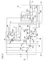
- FIG. 1 shows an embodiment according to the present invention (i.e, electrostatic atomizer).
- This electrostatic atomizer comprises a discharge electrode 1, a counter electrode 2, a cooling source 3, a sensing block 4, a DC power supply 5, a high voltage power supply 6 and a controller 7.
- the discharge electrode 1 has a teardrop-shaped tip 11, and receives negative or positive high voltage (e.g., -4.6kV) from the high voltage power supply 6 when it is discharged.
- the counter electrode 2 is formed into a ring shape of which inner edge functions as a substantial electrode, and is located opposite the tip 11 of the electrode 1 a given distance apart.
- the electrode 2 is also connected with ground.
- the cooling source 3 is formed of, for example, a Peltier module 30 and a heat-radiating fin 31, and cools the discharge electrode 1 to a temperature lower than a dew point temperature of ambient air to form thereon dew as water.
- a base of the electrode 1 is connected with the cold side of the module 30, and the fin 31 is connected with the hot side of the module 30.
- the sensing block 4 is formed of a thermistor 40 that measures a temperature of the Peltier module 30 to provide the controller 7 with a measured temperature signal; a temperature sensor that measures an ambient temperature to provide the controller 7 with a measured temperature signal; a humidity sensor that measures ambient humidity to provide a measured humidity signal to the controller 7; and so on.
- the DC power supply 5 is formed of, for example, a DC/DC converter 50 and son on, and provides the Peltier module 30 with the voltage adjusted in accordance with a duty control signal from the controller 7.
- the supply 5 also supplies the high voltage power supply 6 with voltage (V+).
- the high voltage power supply 6 comprises, for example, a current detector 61, a voltage detector 62 and a high voltage generator 63, and further comprises a voltage stabilizing block 60.
- the detector 61 detects a current (discharge current) flowing between the electrodes 1 and 2, and provides the controller 7 (AD input) with a detected current signal (voltage Vi).
- the detector 62 detects voltage (discharge voltage) applied across the electrodes 1 and 2, and provides the controller 7 (AD input) with a detected voltage signal (voltage Vv).
- the generator 63 generates high voltage for discharge to apply across the electrodes 1 and 2 in accordance with the ON control signal from the controller 7, and also stops generating the high voltage in accordance with the OFF control signal from the controller 7. Details of each part of the power supply 6 is described later.
- the controller 7 is formed of, for example, a micon (microcomputer), a storage device, A/D converters and so on, and controls output of the DC power supply 5 and output of the high voltage power supply 6 based on the voltage and the current from the detectors 61 and 62.
- the power supplies are controlled by various modes such as, for example, a start mode, a discharge current control mode and so on.
- the controller 7 provides the DC power supply 5 with an initial duty control signal for a given time so that the output voltage of the power supply 5 (converter 50) becomes predetermined initial voltage. Thereby, a cooling rate of the Peltier module 30 is adjusted to an initial cooling rate and then dew is formed on the electrode 1. It is allowable to calculate time during which dew is admitted to be formed on the electrode 1 based on each detection value of the sensing block 4 and voltage applied across the module 30, and said given time may be set to the calculated time. Also, the controller 7 may control: to apply high voltage across the electrodes 1 and 2 through the high voltage power supply 6 while stepwise raising voltage of the module 30; and to confirm whether or not dew is formed on the electrode 1 based on the current detected with the current detector 61.
- the controller 7 supplies the ON control signal to the high voltage power supply 6 so that the power supply 6 generates high voltage to apply across the electrodes 1 and 2.
- the controller 7 supplies a duty control signal to the DC power supply 5 so that the cooling rate of the Peltier module 30 is adjusted by adjusting the output voltage of the power supply 5 based on at least the current, of the current detected with the current detector 61 and the voltage detected with the voltage detector 62.
- the controller 7 supplies a duty control signal to the DC power supply 5 so as to raise output voltage of the power supply 5 to raise the cooling rate of the Peltier module 30. Conversely, if a value of current detected with the detector 61 is larger than the value of the reference current, the controller 7 supplies a duty control signal to the power supply 5 so as to lower output voltage of the power supply 5 to lower the cooling rate.
- the current detector 61 is, for example, a summing amplifier circuit formed of an operational amplifier 610, resistors 611-615 and a capacitor 616, and has an input-output (Idc-Vi) characteristic of 0.1V/ ⁇ A as shown in FIG. 3 .
- Vi Vref1 - R615 ⁇ (Iref1 + Idc)
- the summing amplifier circuit can provide the controller 7 with the Vi corresponding to the sum of Idc and Iref1 regardless of the direction of the current Idc (positive or negative) as shown in FIG. 3 .
- the slope of Idc-Vi in FIG. 3 is set with the resistor 615. Since the resistance of the discharge circuit is much high, the resistor 611 is set to a value within the range that does not influence a discharge current and is 100k ⁇ in FIG. 3 .
- the error appears in the output of the detector 61 owing to dispersion in the reference voltage, the offset current and the offset voltage of the operational amplifier 610 and the like.
- the offset voltage of the detector 61 is set so as to measure and reduce the error and is 1.5 [V] in FIG. 3 . Temperature drift depending on temperature change can be cancelled even in operation (e.g., discharge current control mode) by measuring the offset voltage of the detector 61 during discharge stop.
- the voltage detector 62 is also, for example, a summing amplifier circuit formed of an operational amplifier 620, resistors 621-625 and a capacitor 626, and has an input-output (Vdv-Vv) characteristic of 0.5V/kV as shown in FIG. 5 .
- Idv Vdv / R621
- Vv is given by Vref2 - R625 ⁇ (Iref2 - Vdv / R621).
- the slope of Vdv-Vv is set with the resistors 621 and 625 which are 500M ⁇ and 250k ⁇ , respectively in FIG. 5 .
- the high voltage generator 63 can be divided into an ON/OFF circuit 64, a step-up transformer 65, a voltage doubler circuit 66, a oscillation circuit 67 and a control circuit 68.
- the circuit 64 is formed of, for example, a transistor 640 as a switch and a resistor 641, and turns the generator 63 on/off according to the ON/OFF signals from the controller 7, respectively. That is, the transistor 640 turns on the circuit 67 according to the ON control signal (LOW signal) to turn on the generator 63.
- the transistor 640 also turns off the circuit 67 according to the OFF control signal (HIGH signal or OPEN signal) to turn off the generator 63.
- the generator 63 is usually off and generates high voltage only when it is worked.
- the transformer 65 has a primary winding 651 and secondary windings 652 and 653, and respectively induces high voltage and ON voltage across the windings 652 and 653 in response to voltage applied across the winding 651.
- the windings 651 and 653 are also utilized as construction elements of the circuit 67.
- the voltage doubler circuit 66 is formed of, for example, diodes 661 and 662 and capacitors 663 and 664. This circuit 66 adds the high voltage induced across the secondary winding 652 and voltage across the capacitor 663 charged with the high voltage to charge the capacitor 664 with two times of the high voltage, and then applies voltage of the capacitor 664 (negative voltage) across the electrodes 1 and 2. Therefore, constant high voltage is applied across the electrodes 1 and 2 from the capacitor 664.
- the terminal G of FIG. 4 is connected to ground of the oscillation circuit 67 or to ground via the resistor for detecting a discharge current.
- the oscillation circuit 67 is formed of, for example, a transistor 670 as a switching element, resistors 671 and 672 and a capacitor 673 in addition to said windings 651 and 653.
- This circuit 67 itself is an astable oscillator that oscillates in free running mode, but the circuit 67 under control of the control circuit 68 generates oscillation voltage while adjusting off timing of the transistor 670 according to the control and then applies the voltage across the winding 651.
- the capacitor 673 is provided to make switching of the transistor 670 faster and to reduce the switching loss.
- the transistor 670 is rapidly turned on through the positive feedback of the voltage increase, and then voltage (oscillation voltage) is applied across the winding 651 to be stepped up with the transformer 65 and the circuit 66.
- voltage oscillation voltage
- the base current of a transistor corresponding to the transistor 670 is decreased after its collector current reaches the level obtained by multiplying the base current by h FE of the transistor, and then voltage across an inductor corresponding to the winding 651 is reduced, so that the transistor is rapidly turned off.
- off timing of the transistor 670 is controlled through the control circuit. 68.
- the control circuit 68 is formed with, for example, a transistor 680 as a switch element; a transistor 681 as an amplification element (control device) for adjusting off timing of the transistor 670; diodes 682-684; and resistors 685-687.
- the diode 682 is provided in order to prevent voltage across the winding 653 from being applied as reverse bias across each base-emitter of the transistors 640, 670, 680 and 681 when the transistor 670 is turned off.
- the transistor 680, the diodes 683 and 684 and the resistors 685 and 686 are provided to mainly turn the transistor 670 off. That is, when the transistor 670 is rapidly turned on through the positive feedback of the voltage increase, the collector current of the transistor 670 increases in proportion to time. Accordingly, voltage across the resistor 685 increases in proportion to time under control of said control device (681) and then the transistor 680 is turned on with voltage across the resistor 685. As a result, since the diodes 683 and 684 are connected in series between the base of the transistor 670 and ground via the transistor 680, the base current of the transistor 670 is decreased. Thus, once the base current is decreased, the collector current of the transistor 670 is decreased and then the voltage across the winding 561 is lowered.
- the transistor 670 is rapidly turned of through positive feed back of voltage decrease from the winding 651 to the winding 653.
- the fundamental and latest on timing of the transistor 680 is determined by relation between V685 and sum voltage of V680 BE and V680 BG , where V685 is voltage across the resistor 685, and V680 BE and V680 BG are base-emitter voltage of the transistor 680 and the emitter-ground voltage (voltage across the diodes 683 and 684), respectively. Therefore, the resistor 685 is set in consideration of not only the on timing but also the fundamental and latest off timing of the transistor 670. In other words, the peak current of the resistor 685 is decreased and restricted.
- the transistor 681 and the resistor 687 adjust on timing of the transistor 680 within range restricted with the diodes 683 and 684 in response to voltage (Vv) detected with the voltage detector 62, and then adjust off timing of the transistor 670. That is, since the transistor 681 is connected in parallel with the diodes 683 and 684, said sum voltage is adjusted in accordance with the input-output (Vv corresponding to discharge voltage-collector voltage) characteristic of the transistor 681 shown in "A" of FIG. 6 .
- the high voltage generator 63 can stably generate high voltage in response to voltage detected with the voltage detector 62.
- the voltage stabilizing block 60 is provided in order to generate high voltage more stably. That is, the high voltage generator 63 includes the transistor 681 and the voltage stabilizing block 60 that are opposite to each other in temperature characteristic, and this block 60 is formed of, for example, a zener diode 600. Accordingly, the transistor 681 operates to receive the voltage detected with the detector 62 via the voltage stabilizing block 60 and to adjust the high voltage applied across the electrodes 1 and 2 through feedback control so that the received voltage corresponds to specified discharge voltage (voltage corresponding to Iref2).
- the input-output characteristic of the transistor 681 becomes a characteristic such as "B" of FIG. 6 .
- the base-emitter voltage of the transistor 681 is lowered in response to rise of ambient temperature, the discharge voltage between the electrodes 1 and 2 is lowered.
- the transistor 681 has negative temperature characteristic of about -3mV/°C at PN junction between the base-emitter. Accordingly, the voltage stabilizing block 60 is provided, and is preferably located in proximity to the transistor 681. The block 60 has temperature characteristic that is opposite to the temperature characteristic of the transistor 681. Also, from the relation like said formula, the block 60 and the resistor 687 are set so that output voltage of the voltage detector 62 corresponds to desired discharge voltage.
- the block 60 is formed of the zener diode 600
- the zener diode is used, of which temperature coefficient is zero around 5V and becomes positive in equal to or more than 5V
- the level of the discharge voltage can be also controlled with higher accuracy than that in case of resistor, through the steep characteristic of "A" in FIG. 6 .
- the voltage stabilizing block 60 of the high voltage power supply 6 is formed of the zener diode 600 and a resistor (fixed resistor or variable resistor) 601.
- the resistor 601 is a variable resistor
- the input-output characteristic of the transistor 681 can be changed as shown in FIG. 8 .
- the voltage stabilizing block 60 is formed of a transistor 602 and resistors 603 and 604.
- the transistor 681 has an input-output characteristic such as "C" of FIG. 6 .
- the controller 7 supplies a duty control signal to the DC power supply 5 so as to adjust cooling rate of the Peltier module 30 by adjusting output voltage of the power supply 5 based on the current detected with the current detector 61 and the voltage detected with the voltage detector 62.
- discharge voltage V(m)
- Table 1 the voltage across the electrodes 1 and 2 changes, a value of discharge current showing quantity of dew formed on the discharge electrode 1 changes as well. Accordingly, the voltage (discharge voltage) detected with the detector 62 is further utilized.
- predetermined mid-value Imid(n) value of reference current
- maximum value Imax(n) threshold Imax
- minimum value Imin(n) are selected every discharge voltage V(m). Therefore, the controller 7 supplies a duty control signal to the power supply 5 so that a current detected with the detector 61 becomes the mid-value corresponding to voltage detected with the detector 62.
- the controller 7 also supplies a duty control signal to the DC power supply 5 so that a cooling rate of the Peltier module 30 approximates to the cooling rate corresponding to the mid-value without overshoot, based on the current detected with the current detector 61 and the voltage detected with the voltage detector 62. Specifically, after stability of each block of the electrostatic atomizer, the controller 7 averages the current and voltage detected with the detectors 61 and 62 every specified period ⁇ t. For example, when each block is stable (t0), the controller 7 starts picking up the current and voltage from the detectors 61 and 62.
- the increment ⁇ D(m) may be calculated by using a correction function F ⁇ D(m-1) ⁇ in response to a value of the previous increment ⁇ D(m-1),i.e., by (Pa ⁇ ⁇ Id(m) - Pb ⁇ ⁇ I(m)) ⁇ F ⁇ D(m-1) ⁇ .
- the function F ⁇ D(m) has a small value in case that the previous duty D(m-1) is low, and has a large value in case that D(m-1) is high. Thereby, it is possible to weight the whole duty.
Landscapes
- Electrostatic Spraying Apparatus (AREA)
Abstract
Description
- The invention relates generally to electrostatic atomizers and more particularly to an electrostatic atomizer that generates mist of charged fine particles in the order of nanometer in size.
- Such sort of electrostatic atomizer is seen in, for example, the patent document of
Japanese Patent Number 3260150 European orPatent Publication Number 0 486 198 A1United States Patent Number 5,337,963 ). A prior art device described in the document comprises a cartridge for storage of liquid suitable for electrostatic spraying, and a high voltage means for applying electrostatic potential to the liquid. The cartridge includes a capillary structure that extends into the interior of the cartridge so as to feed liquid by capillary action from the cartridge to a spraying outlet at a tip of the capillary structure. The cartridge also includes a means for providing an electrically conductive path to allow the application of an electrostatic charge to the liquid. When the high voltage means applies the potential to the liquid at the mouth of the spraying outlet, a potential gradient is developed between innermost and outermost peripheral surfaces of the mouth, and draws the liquid across an end face of the spraying outlet towards the outermost peripheral surface. Thereby, the liquid is projected electrostatically as an array of ligaments which form a halo around the mouth. - However, the prior art device requires that water is supplied into the cartridge. Also, an electrostatic atomizer that can solve this issue has been separately made by the applicant (see
Japanese Patent Application Publication Number 2006-122819 - Incidentally, the atomizer repeats the Rayleigh splitting to realize electrostatic atomization. That is, when high voltage is applied across the electrodes, a negative electronic charge concentrates on the discharge electrode, and also water held on the tip of the discharge electrode rises like a cone to form a Taylor cone. When the negative electronic charge concentrates on the tip of the Taylor cone to become high density, repulsion of the electronic charge in the high density brings about Rayleigh splitting to split and scatter the Taylor cone shaped water. Thus, in the atomizer that repeats the Rayleigh splitting to realize electrostatic atomization, stable generation of high voltage is important.
- It is therefore an object of the present invention to stably generate high voltage for forming mist of charged fine particles in the order of nanometer in size in addition to saving the trouble of supplying water.
- An electrostatic atomizer of the present invention comprises a discharge electrode, a counter electrode located opposite the discharge electrode, a cooling source that cools the discharge electrode to form thereon dew as water, a high voltage power supply that applies high voltage for discharge across the electrodes, and a voltage detector that detects voltage between the electrodes. The power supply includes a control device and a voltage stabilizing device that are opposite to each other in temperature characteristic. The control device is configured to pick up the voltage detected with the detector via the voltage stabilizing device, and to adjust the high voltage applied across the electrodes through feedback control so that the voltage corresponds to specified discharge voltage. In this configuration, the discharge voltage between the electrodes is stabilized to the specified discharge voltage. Therefore, even under unstable temperature conditions, it is possible to stably generate high voltage for forming mist of charged fine particles in the order of nanometer in size.
- Preferably, the atomizer further comprises a current detector that detects a current flowing between the electrodes, and a controller that adjusts a cooling rate of the cooling source based on a value of a predetermined specified current. The controller raises the rate when a value of the current detected with the current detector is smaller than the value of the specified current, and lowers the rate when the value of the current is larger than the value of the specified current. In this configuration, it is possible to suitably adjust quantity of the dew formed on the discharge electrode.
- Preferably, the control device is a transistor, and the voltage stabilizing device has the opposite temperature characteristic in comparison with the temperature characteristic between the base and emitter of the control device.
- It is preferable that the atomizer further comprises a resister for adjusting the high voltage of the power supply. In this case, the resister is connected in series with the voltage stabilizing device. In this configuration, the high voltage can be adjusted with a value of the resistor.
- Preferred embodiments of the invention will now be described in further details. Other features and advantages of the present invention will become better understood with regard to the following detailed description and accompanying drawings where:
-
FIG. 1 is a schematic diagram of an embodiment according to the present invention; -
FIG. 2 is a circuit diagram of mainly a current detector ofFIG. 1 ; -
FIG. 3 illustrates an input-output characteristic of the current detector ofFIG. 2 ; -
FIG. 4 is a circuit diagram of a high voltage power supply ofFIG. 1 ; -
FIG. 5 illustrates an input-output characteristic of a voltage detector ofFIG. 4 ; -
FIG. 6 illustrates an input-output characteristic of a control device ofFIG. 4 ; -
FIG. 7 is a circuit diagram of a voltage stabilizing block in an alternate embodiment; -
FIG. 8 illustrates an input-output characteristic of a control device in the embodiment ofFIG. 7 ; -
FIG. 9 is a circuit diagram of a voltage stabilizing block in another alternate embodiment; and -
FIG. 10 is an explanatory diagram of discharge current control in an enhanced embodiment. -
FIG. 1 shows an embodiment according to the present invention (i.e, electrostatic atomizer). This electrostatic atomizer comprises adischarge electrode 1, acounter electrode 2, acooling source 3, asensing block 4, aDC power supply 5, a highvoltage power supply 6 and acontroller 7. - The
discharge electrode 1 has a teardrop-shaped tip 11, and receives negative or positive high voltage (e.g., -4.6kV) from the highvoltage power supply 6 when it is discharged. Thecounter electrode 2 is formed into a ring shape of which inner edge functions as a substantial electrode, and is located opposite thetip 11 of the electrode 1 a given distance apart. Theelectrode 2 is also connected with ground. - The
cooling source 3 is formed of, for example, aPeltier module 30 and a heat-radiatingfin 31, and cools thedischarge electrode 1 to a temperature lower than a dew point temperature of ambient air to form thereon dew as water. A base of theelectrode 1 is connected with the cold side of themodule 30, and thefin 31 is connected with the hot side of themodule 30. - The
sensing block 4 is formed of athermistor 40 that measures a temperature of the Peltiermodule 30 to provide thecontroller 7 with a measured temperature signal; a temperature sensor that measures an ambient temperature to provide thecontroller 7 with a measured temperature signal; a humidity sensor that measures ambient humidity to provide a measured humidity signal to thecontroller 7; and so on. - The
DC power supply 5 is formed of, for example, a DC/DC converter 50 and son on, and provides the Peltiermodule 30 with the voltage adjusted in accordance with a duty control signal from thecontroller 7. Thesupply 5 also supplies the highvoltage power supply 6 with voltage (V+). - The high
voltage power supply 6 comprises, for example, acurrent detector 61, avoltage detector 62 and ahigh voltage generator 63, and further comprises avoltage stabilizing block 60. Thedetector 61 detects a current (discharge current) flowing between theelectrodes detector 62 detects voltage (discharge voltage) applied across theelectrodes generator 63 generates high voltage for discharge to apply across theelectrodes controller 7, and also stops generating the high voltage in accordance with the OFF control signal from thecontroller 7. Details of each part of thepower supply 6 is described later. - The
controller 7 is formed of, for example, a micon (microcomputer), a storage device, A/D converters and so on, and controls output of theDC power supply 5 and output of the highvoltage power supply 6 based on the voltage and the current from thedetectors - For example, in case of the start mode (when it is started), the
discharge electrode 1 is not yet cooled and dew is not formed on theelectrode 1. Because of this, thecontroller 7 provides theDC power supply 5 with an initial duty control signal for a given time so that the output voltage of the power supply 5 (converter 50) becomes predetermined initial voltage. Thereby, a cooling rate of the Peltiermodule 30 is adjusted to an initial cooling rate and then dew is formed on theelectrode 1. It is allowable to calculate time during which dew is admitted to be formed on theelectrode 1 based on each detection value of thesensing block 4 and voltage applied across themodule 30, and said given time may be set to the calculated time. Also, thecontroller 7 may control: to apply high voltage across theelectrodes voltage power supply 6 while stepwise raising voltage of themodule 30; and to confirm whether or not dew is formed on theelectrode 1 based on the current detected with thecurrent detector 61. - In case of the discharge current control mode, the
controller 7 supplies the ON control signal to the highvoltage power supply 6 so that thepower supply 6 generates high voltage to apply across theelectrodes controller 7 supplies a duty control signal to theDC power supply 5 so that the cooling rate of thePeltier module 30 is adjusted by adjusting the output voltage of thepower supply 5 based on at least the current, of the current detected with thecurrent detector 61 and the voltage detected with thevoltage detector 62. Thereby, when a discharge is generated between theelectrodes discharge electrode 1, the water on theelectrode 1 is pulled toward thecounter electrode 2 side to shape a Taylor cone. Rayleigh splitting then occurs at the tip of the Taylor cone, so that mist of charged fine particles in the order of nanometer in size is generated. - In order to generate the mist stably, it is necessary to adjust quantity of the dew on the
discharge electrode 1 to appropriate quantity determined at design stage (specified quantity within specified range). If the quantity of dew on theelectrode 1 is much less than the specified quantity, the discharge occurs not between the water and thecounter electrode 2 but between theelectrodes electrode 1 is much greater than the specified quantity, a short circuit current flows between the water and theelectrode 2 that are shorter, which makes it impossible to generate mist of charged fine particles of object size. On account of this, in the discharge current control mode, relation between current (discharge current) detected with thecurrent detector 61 and length of the Taylor cone is utilized. That is, if the quantity of dew on theelectrode 1 is little, the length of the Taylor cone becomes short and a value of current detected with thedetector 61 becomes small. On the other hand, if the quantity of dew on theelectrode 1 is much, the length of the Taylor cone becomes long and a value of current detected with thedetector 61 becomes large. Thus, by detecting a current flowing between theelectrodes detector 61, the length of the Taylor cone (quantity of dew) can be known. Accordingly, if a value of current detected with thedetector 61 is smaller than the value of a predetermined reference current, thecontroller 7 supplies a duty control signal to theDC power supply 5 so as to raise output voltage of thepower supply 5 to raise the cooling rate of thePeltier module 30. Conversely, if a value of current detected with thedetector 61 is larger than the value of the reference current, thecontroller 7 supplies a duty control signal to thepower supply 5 so as to lower output voltage of thepower supply 5 to lower the cooling rate. - Each part of the high
voltage power supply 6 is herein explained in detail: As shown inFIG. 2 , thecurrent detector 61 is, for example, a summing amplifier circuit formed of anoperational amplifier 610, resistors 611-615 and acapacitor 616, and has an input-output (Idc-Vi) characteristic of 0.1V/µA as shown inFIG. 3 . That is, thedetector 61 picks up the current Idc flowing between theelectrodes resistor 611 inserted into the discharge circuit, and adds the current Idc to a reference current Iref1 and then provides thecontroller 7 with voltage Vi corresponding to the sum of Idc and Iref1 (Vi = Vref1 - R615 × (Iref1 + Idc)), where Vref1 is reference voltage and R615 is resistance of theresistor 615. InFig. 2 , since the direction of the current Idc corresponds to negative, the voltage Vi is given by Vref1 - R615 × (Iref1 - Idc). But the summing amplifier circuit can provide thecontroller 7 with the Vi corresponding to the sum of Idc and Iref1 regardless of the direction of the current Idc (positive or negative) as shown inFIG. 3 . The slope of Idc-Vi inFIG. 3 is set with theresistor 615. Since the resistance of the discharge circuit is much high, theresistor 611 is set to a value within the range that does not influence a discharge current and is 100kΩ inFIG. 3 . Thedetector 61 is also configured to include offset voltage (Vi in case of Idc = 0) for reducing error of the detection result (Vi) caused by dispersion in circuit parts. That is, the error appears in the output of thedetector 61 owing to dispersion in the reference voltage, the offset current and the offset voltage of theoperational amplifier 610 and the like. The offset voltage of thedetector 61 is set so as to measure and reduce the error and is 1.5 [V] inFIG. 3 . Temperature drift depending on temperature change can be cancelled even in operation (e.g., discharge current control mode) by measuring the offset voltage of thedetector 61 during discharge stop. - As shown in
FIG. 4 , thevoltage detector 62 is also, for example, a summing amplifier circuit formed of anoperational amplifier 620, resistors 621-625 and acapacitor 626, and has an input-output (Vdv-Vv) characteristic of 0.5V/kV as shown inFIG. 5 . That is, thedetector 62 picks up a current Idv (Idv = Vdv / R621) as the voltage Vdv applied across theelectrodes resistor 621 connected with the output of thehigh voltage generator 63, and adds the current Idv to a reference current Iref2 and then provides thecontroller 7 with voltage Vv corresponding to the sum of Idv and Iref2 (Vv = Vref2 - R625 × (Iref2 + Vdv / R621)), where Vref2 is reference voltage and R621 and R625 are resistance of theresistors Fig. 4 , since the direction of the current Idv corresponds to negative, the voltage Vv is given by Vref2 - R625 × (Iref2 - Vdv / R621). The slope of Vdv-Vv is set with theresistors FIG. 5 . Thedetector 62 also includes offset voltage (Vv in case of Vdv = 0) in the same way as thedetector 61 and is .1.5 [V] inFIG. 5 . Temperature drift depending on temperature change can be cancelled even in operation by measuring the offset voltage of thedetector 62 during discharge stop. - As shown in
FIG. 4 , thehigh voltage generator 63 can be divided into an ON/OFF circuit 64, a step-uptransformer 65, avoltage doubler circuit 66, aoscillation circuit 67 and acontrol circuit 68. Thecircuit 64 is formed of, for example, atransistor 640 as a switch and aresistor 641, and turns thegenerator 63 on/off according to the ON/OFF signals from thecontroller 7, respectively. That is, thetransistor 640 turns on thecircuit 67 according to the ON control signal (LOW signal) to turn on thegenerator 63. Thetransistor 640 also turns off thecircuit 67 according to the OFF control signal (HIGH signal or OPEN signal) to turn off thegenerator 63. In short, thegenerator 63 is usually off and generates high voltage only when it is worked. Thetransformer 65 has a primary winding 651 andsecondary windings windings windings 651 and 653 are also utilized as construction elements of thecircuit 67. - The
voltage doubler circuit 66 is formed of, for example,diodes capacitors circuit 66 adds the high voltage induced across the secondary winding 652 and voltage across thecapacitor 663 charged with the high voltage to charge thecapacitor 664 with two times of the high voltage, and then applies voltage of the capacitor 664 (negative voltage) across theelectrodes electrodes capacitor 664. The terminal G ofFIG. 4 is connected to ground of theoscillation circuit 67 or to ground via the resistor for detecting a discharge current. - The
oscillation circuit 67 is formed of, for example, atransistor 670 as a switching element,resistors capacitor 673 in addition to saidwindings 651 and 653. Thiscircuit 67 itself is an astable oscillator that oscillates in free running mode, but thecircuit 67 under control of thecontrol circuit 68 generates oscillation voltage while adjusting off timing of thetransistor 670 according to the control and then applies the voltage across the winding 651. Thecapacitor 673 is provided to make switching of thetransistor 670 faster and to reduce the switching loss. - That is, when the
transistor 640 is turned off according to the ON control signal from condition that thetransistor 640 is held on according to the OFF control signal to hold thetransistor 670 off, voltage V+ is applied to the base of thetransistor 670 through theresistor 671, the winding 653 and theresistor 672. A base current then flows between the base-emitter of thetransistor 670. Thereby, the collector voltage of thetransistor 670 is reduced by voltage across its collector-emitter and corresponding voltage is applied across the winding 651. Then, induction voltage is induced across the winding 653 magnetically coupled to the winding 651 through positive feedback of the voltage increase from the winding 651 to the winding 653 and then is applied to the base of thetransistor 670. Consequently, thetransistor 670 is rapidly turned on through the positive feedback of the voltage increase, and then voltage (oscillation voltage) is applied across the winding 651 to be stepped up with thetransformer 65 and thecircuit 66. In a general astable oscillator, for example, the base current of a transistor corresponding to thetransistor 670 is decreased after its collector current reaches the level obtained by multiplying the base current by hFE of the transistor, and then voltage across an inductor corresponding to the winding 651 is reduced, so that the transistor is rapidly turned off. But in the embodiment, off timing of thetransistor 670 is controlled through the control circuit. 68. - The
control circuit 68 is formed with, for example, atransistor 680 as a switch element; atransistor 681 as an amplification element (control device) for adjusting off timing of thetransistor 670; diodes 682-684; and resistors 685-687. Thediode 682 is provided in order to prevent voltage across the winding 653 from being applied as reverse bias across each base-emitter of thetransistors transistor 670 is turned off. - The
transistor 680, thediodes resistors transistor 670 off. That is, when thetransistor 670 is rapidly turned on through the positive feedback of the voltage increase, the collector current of thetransistor 670 increases in proportion to time. Accordingly, voltage across theresistor 685 increases in proportion to time under control of said control device (681) and then thetransistor 680 is turned on with voltage across theresistor 685. As a result, since thediodes transistor 670 and ground via thetransistor 680, the base current of thetransistor 670 is decreased. Thus, once the base current is decreased, the collector current of thetransistor 670 is decreased and then the voltage across the winding 561 is lowered. Therefore, thetransistor 670 is rapidly turned of through positive feed back of voltage decrease from the winding 651 to the winding 653. The fundamental and latest on timing of thetransistor 680 is determined by relation between V685 and sum voltage of V680BE and V680BG, where V685 is voltage across theresistor 685, and V680BE and V680BG are base-emitter voltage of thetransistor 680 and the emitter-ground voltage (voltage across thediodes 683 and 684), respectively. Therefore, theresistor 685 is set in consideration of not only the on timing but also the fundamental and latest off timing of thetransistor 670. In other words, the peak current of theresistor 685 is decreased and restricted. - The
transistor 681 and theresistor 687 adjust on timing of thetransistor 680 within range restricted with thediodes voltage detector 62, and then adjust off timing of thetransistor 670. That is, since thetransistor 681 is connected in parallel with thediodes transistor 681 shown in "A" ofFIG. 6 . Specifically, if a current Idv corresponding to discharge voltage Vdv across theelectrodes transistor 681 become higher and the collect voltage of thetransistor 681 becomes lower in accordance with the characteristic A ofFIG. 6 . Therefore, the sum voltage becomes lower. Thereby, since on timing of thetransistor 680 becomes earlier and off timing of thetransistor 670 becomes earlier, the voltage Vdv can be lowered. Conversely, if the current Idv becomes smaller than the reference current Iref2, the voltage Vv and base voltage of thetransistor 681 become lower and the collect voltage of thetransistor 681 becomes higher, and therefore the sum voltage becomes higher. Thereby, since on timing of thetransistor 680 becomes later and off timing of thetransistor 670 becomes later, voltage Vdv can be raised. Thus, by repeatedly turning thetransistor 670 on and off to apply oscillation voltage across the winding 651, it is possible to stably generate high voltage through thehigh voltage generator 63. - As mentioned above, the
high voltage generator 63 can stably generate high voltage in response to voltage detected with thevoltage detector 62. In the embodiment, thevoltage stabilizing block 60 is provided in order to generate high voltage more stably. That is, thehigh voltage generator 63 includes thetransistor 681 and thevoltage stabilizing block 60 that are opposite to each other in temperature characteristic, and thisblock 60 is formed of, for example, azener diode 600. Accordingly, thetransistor 681 operates to receive the voltage detected with thedetector 62 via thevoltage stabilizing block 60 and to adjust the high voltage applied across theelectrodes - If a resistor of resistance R is utilized instead of the
voltage stabilizing block 60, the input-output characteristic of thetransistor 681 becomes a characteristic such as "B" ofFIG. 6 . In this characteristic, the relation of Vv = (1 + R /R687) × V681BE is satisfied when thetransistor 681 is operated, where R687 is resistance of theresistor 687 and V681BE is the base-emitter voltage of the transistor 681 (about 0.7 V). In this case, when the base-emitter voltage of thetransistor 681 is lowered in response to rise of ambient temperature, the discharge voltage between theelectrodes - In the embodiment, it is considered that the
transistor 681 has negative temperature characteristic of about -3mV/°C at PN junction between the base-emitter. Accordingly, thevoltage stabilizing block 60 is provided, and is preferably located in proximity to thetransistor 681. Theblock 60 has temperature characteristic that is opposite to the temperature characteristic of thetransistor 681. Also, from the relation like said formula, theblock 60 and theresistor 687 are set so that output voltage of thevoltage detector 62 corresponds to desired discharge voltage. In case that theblock 60 is formed of thezener diode 600, the zener diode is used, of which temperature coefficient is zero around 5V and becomes positive in equal to or more than 5V Thereby, it is possible to cancel the negative temperature coefficient of thetransistor 681 and tune the temperature coefficient of thehigh voltage generator 63 to zero. Thus, by providing theblock 60, discharge voltage variation caused by ambient temperature change can be prevented and high voltage can be generated more stably. The level of the discharge voltage can be also controlled with higher accuracy than that in case of resistor, through the steep characteristic of "A" inFIG. 6 . - In an alternate embodiment, as shown in
FIG. 7 , thevoltage stabilizing block 60 of the highvoltage power supply 6 is formed of thezener diode 600 and a resistor (fixed resistor or variable resistor) 601. In case that theresistor 601 is a variable resistor, the input-output characteristic of thetransistor 681 can be changed as shown inFIG. 8 . - In another alternate embodiment, as shown in
FIG. 9 , thevoltage stabilizing block 60 is formed of atransistor 602 andresistors transistor 681 has an input-output characteristic such as "C" ofFIG. 6 . - In an enhanced embodiment, the
controller 7 supplies a duty control signal to theDC power supply 5 so as to adjust cooling rate of thePeltier module 30 by adjusting output voltage of thepower supply 5 based on the current detected with thecurrent detector 61 and the voltage detected with thevoltage detector 62. Herein, discharge voltage (V(m)) is previously selected by a user from voltage ranges shown in Table 1. Because of this, if voltage across theelectrodes discharge electrode 1 changes as well. Accordingly, the voltage (discharge voltage) detected with thedetector 62 is further utilized. In addition, as shown in Table 1, predetermined mid-value Imid(n) (value of reference current), maximum value Imax(n) (threshold Imax) and minimum value Imin(n) are selected every discharge voltage V(m). Therefore, thecontroller 7 supplies a duty control signal to thepower supply 5 so that a current detected with thedetector 61 becomes the mid-value corresponding to voltage detected with thedetector 62. -
[Table 1] Discharge Voltage V(m) [-kV] Discharge Curent I(m) [µA] Minimum Value Imin(n) Mid-Value Imid(n) Maximum Value Imax(n) 4.1 ≦ V(m)<4.2 Imin(1) = I1-A1 Imid(1) = I1 Imax(1) = I1+A1 4.2≦V(m)<4.3 Imin(2) = I2-A2 Imid(2) = I2 Imax(2) = I2+A2 4.3≦V(m)<4.4 Imin(3) = I3-A3 Imid(3) = I3 Imax(3) = I3+A3 4.4≦V(m)<4.5 Imin(4) = I4-A4 Imid(4) = I4 Imax(4) = I4+A4 4.5≦V(m)<4.6 Imin(5) = I5-A5 Imid(5) = I5 Imax(5) = I6+A5 4.6≦V(m)<4.7 Imin(6) = I6-A6 Imid(6) = I6 Imax(6) = I6+A6 4.7≦V(m)<4.8 Imin(7) = I7-A7 Imid(7) = I7 Imax(7) = I7+A7 4.8≦V(m)<4.9 Imin(8) = I8-A8 Imid(8) = I8 Imax(8) = I8+A8 4.9≦V(m)<5.0 Imin(9) = I9-A9 Imid(9) = I9 Imax(9) = I9+A9 5.0≦V(m)<5.1 Imin(10) = I10-A10 Imid(10) = I10 Imax(10) = I10+A10 5.1≦V(m)<5.2 Imin(11) = I11-A11 Imid(11) = I11 Imax(11) = I11+A11 - As shown in
FIG. 10 , thecontroller 7 also supplies a duty control signal to theDC power supply 5 so that a cooling rate of thePeltier module 30 approximates to the cooling rate corresponding to the mid-value without overshoot, based on the current detected with thecurrent detector 61 and the voltage detected with thevoltage detector 62. Specifically, after stability of each block of the electrostatic atomizer, thecontroller 7 averages the current and voltage detected with thedetectors controller 7 starts picking up the current and voltage from thedetectors controller 7 calculates a mean value of the current values and a mean value of the voltage values as discharge current I(1) and discharge voltage V(1), respectively. Similarly, at a point in time t2, thecontroller 7 calculates discharge current I(2) and discharge voltage V(2). At this point, thecontroller 7 calculates the difference in discharge currents between t1 and t2 (ΔI(2) = I(2) - I(1)) and reads mid-value (Imid(n), t = t1) corresponding to V(1) from Table 1. And thecontroller 7 calculates the difference (ΔId(2) = Imid(n){t=t1} - I(2)) from I(2). Thecontroller 7 then calculates increment (ΔD(2) = Pa × ΔId(2) - Pb × ΔI(2)) for duty (D(3)) with respect to thepower supply 5 between t2 and t3, and figures out duty between t2 and t3 (D(3) = D(2) + ΔD(2)) from duty between t1 and t2 (D(2)), where Pa and Pb are parameters and D(2), D(3) or the like corresponds to any of D1-D256 obtained by dividing duty of 0-100% into 256. After t3 as well, thecontroller 7 calculates duty increment (ΔD(m) = Pa × ΔId(m) - Pb × ΔI(m)) and then supplies a duty control signal to thepower supply 5. - However, in case that the duty increment ΔD(m) is calculated, the increment ΔD(m) may be calculated by using a correction function F{D(m-1)} in response to a value of the previous increment ΔD(m-1),i.e., by (Pa × ΔId(m) - Pb × ΔI(m)) × F{D(m-1)}. The function F{D(m) has a small value in case that the previous duty D(m-1) is low, and has a large value in case that D(m-1) is high. Thereby, it is possible to weight the whole duty. When duty is low, voltage to the
Peltier module 30 is also low and cooling temperature ΔT of thedischarge electrode 1 is low domain as well, and therefore dew is easily formed thereon. Accordingly, it is possible to prevent excess dew from being formed by setting the value of the correction function to, for example, 0.5. Conversely, when duty is high, cooling temperature ΔT is also high and dew is hardly formed, and therefore the value of the correction function is set to, for example, 2 in order to enlarge rate of change. For example, in case of high humidity in which room temperature is 25°C and dew point is 20°C, ΔT is 5°C. Also, in case of low humidity in which room temperature is 25°C and dew point is 10°C, ΔT is 15°C. - Although the present invention has been described with reference to certain preferred embodiments, numerous modifications and variations can be made by those skilled in the art without departing from the true spirit and scope of this invention.
Claims (5)
- An electrostatic atomizer, comprising:a discharge electrode;a counter electrode located opposite the discharge electrode;a cooling source that cools the discharge electrode to form thereon dew as water;a high voltage power supply that applies high voltage for discharge across the electrodes; anda voltage detector that detects voltage between the electrodes;wherein the power supply includes a control device and a voltage stabilizing device that are opposite to each other in temperature characteristic,the control device operating: to pick up the voltage detected with the detector via the voltage stabilizing device; and to adjust the high voltage applied across the electrodes through feedback control so that the voltage corresponds to specified discharge voltage.
- The electrostatic atomizer of claim 1, further comprising:a current detector that detects a current flowing between the electrodes; anda controller that adjusts a cooling rate of the cooling source based on a value of a predetermined specified current;wherein the controller raises the cooling rate when a value of the current detected with the current detector is smaller than the value of the specified current, and lowers the rate when the value of the current is larger than the value of the specified current.
- The electrostatic atomizer of claim 2, wherein:the control device is a transistor; andthe voltage stabilizing device has the opposite temperature characteristic in comparison with the temperature characteristic between the base and emitter of the control device.
- The electrostatic atomizer of claim 2, further comprising a resister for adjusting the high voltage of the power supply, the resister being connected in series with the voltage stabilizing device.
- The electrostatic atomizer of claim 3, further comprising a resister for adjusting the high voltage of the power supply, the resister being connected in series with the voltage stabilizing device.
Applications Claiming Priority (2)
| Application Number | Priority Date | Filing Date | Title |
|---|---|---|---|
| JP2005207579A JP4329739B2 (en) | 2005-07-15 | 2005-07-15 | Electrostatic atomizer |
| PCT/JP2006/314098 WO2007010871A1 (en) | 2005-07-15 | 2006-07-14 | Electrostatic atomizer |
Publications (4)
| Publication Number | Publication Date |
|---|---|
| EP1908527A1 true EP1908527A1 (en) | 2008-04-09 |
| EP1908527A4 EP1908527A4 (en) | 2012-02-29 |
| EP1908527B1 EP1908527B1 (en) | 2013-03-06 |
| EP1908527B8 EP1908527B8 (en) | 2013-06-19 |
Family
ID=37668752
Family Applications (1)
| Application Number | Title | Priority Date | Filing Date |
|---|---|---|---|
| EP06768257.5A Not-in-force EP1908527B8 (en) | 2005-07-15 | 2006-07-14 | Electrostatic atomizer |
Country Status (4)
| Country | Link |
|---|---|
| US (1) | US7861954B2 (en) |
| EP (1) | EP1908527B8 (en) |
| JP (1) | JP4329739B2 (en) |
| WO (1) | WO2007010871A1 (en) |
Cited By (4)
| Publication number | Priority date | Publication date | Assignee | Title |
|---|---|---|---|---|
| EP2065095A1 (en) * | 2007-11-27 | 2009-06-03 | Panasonic Electric Works Co., Ltd | Electrostatically atomizing device with starting voltage control |
| WO2010013824A1 (en) * | 2008-07-28 | 2010-02-04 | Panasonic Electric Works Co., Ltd. | Electrostatic atomizing device and air conditioner using same |
| US8056839B2 (en) | 2007-11-27 | 2011-11-15 | Panasonic Electric Works Co., Ltd. | Electrostatic atomizer |
| CN103566444A (en) * | 2013-11-12 | 2014-02-12 | 江苏大学 | Medical salt mist measuring and control instrument and salt mist concentration quantitative control method |
Families Citing this family (15)
| Publication number | Priority date | Publication date | Assignee | Title |
|---|---|---|---|---|
| CN101669002B (en) * | 2007-04-26 | 2012-11-28 | 松下电器产业株式会社 | Refrigerator, and electric device |
| JP5368726B2 (en) * | 2008-04-18 | 2013-12-18 | パナソニック株式会社 | Electrostatic atomizer |
| JP2010064056A (en) * | 2008-09-12 | 2010-03-25 | Panasonic Electric Works Co Ltd | Electrostatic atomizing device |
| JP5265999B2 (en) * | 2008-09-12 | 2013-08-14 | パナソニック株式会社 | Electrostatic atomizer |
| JP2011067746A (en) | 2009-09-25 | 2011-04-07 | Panasonic Electric Works Co Ltd | Electrostatic atomizer |
| EP2480946A1 (en) * | 2009-09-25 | 2012-08-01 | Panasonic Corporation | Cooling control circuit for peltier device |
| JP2011073617A (en) * | 2009-09-30 | 2011-04-14 | Panasonic Electric Works Co Ltd | Electrostatic atomization device for vehicle |
| JP5654822B2 (en) * | 2010-09-30 | 2015-01-14 | パナソニック株式会社 | Electrostatic atomizer |
| US8701389B2 (en) * | 2011-12-06 | 2014-04-22 | Tenneco Automotive Operating Company Inc. | Reagent injector control system |
| CN103616486B (en) * | 2013-12-11 | 2015-04-22 | 天津开发区合普工贸有限公司 | Totally closed composite nano aerosol high-concentration atomization experiment device |
| JP6444820B2 (en) * | 2015-07-01 | 2018-12-26 | ランズバーグ・インダストリー株式会社 | Electrostatic coating device and electrostatic coating machine |
| CN108970823B (en) * | 2017-05-31 | 2021-08-06 | 北京小米移动软件有限公司 | A device for generating water particles |
| CN206810524U (en) * | 2017-05-31 | 2017-12-29 | 北京小米移动软件有限公司 | A kind of water particulate generating means |
| JP6709961B2 (en) * | 2017-08-31 | 2020-06-17 | パナソニックIpマネジメント株式会社 | Voltage application device and discharge device |
| JP6902721B2 (en) * | 2018-08-29 | 2021-07-14 | パナソニックIpマネジメント株式会社 | Voltage application device and discharge device |
Family Cites Families (10)
| Publication number | Priority date | Publication date | Assignee | Title |
|---|---|---|---|---|
| JPS62173650A (en) | 1986-01-28 | 1987-07-30 | Matsushita Electric Ind Co Ltd | Optical information reproducing device |
| JPS6410712U (en) | 1987-07-08 | 1989-01-20 | ||
| DK0486198T3 (en) | 1990-11-12 | 2001-06-18 | Procter & Gamble | Injection device |
| JPH0832181B2 (en) | 1991-03-08 | 1996-03-27 | 株式会社東芝 | Power supply circuit |
| JP3255805B2 (en) | 1994-09-07 | 2002-02-12 | 株式会社リコー | Switching power supply |
| JP3608661B2 (en) | 2000-09-26 | 2005-01-12 | シャープ株式会社 | Ion generator and air conditioner using the same |
| JP4016934B2 (en) | 2003-10-30 | 2007-12-05 | 松下電工株式会社 | Electrostatic atomizer |
| JP4329672B2 (en) | 2004-10-28 | 2009-09-09 | パナソニック電工株式会社 | Electrostatic atomizer |
| US7567420B2 (en) * | 2004-04-08 | 2009-07-28 | Matsushita Electric Works, Ltd. | Electrostatically atomizing device |
| JP4123203B2 (en) | 2004-07-15 | 2008-07-23 | 松下電器産業株式会社 | Air conditioner |
-
2005
- 2005-07-15 JP JP2005207579A patent/JP4329739B2/en not_active Expired - Lifetime
-
2006
- 2006-07-14 US US11/988,687 patent/US7861954B2/en not_active Expired - Fee Related
- 2006-07-14 WO PCT/JP2006/314098 patent/WO2007010871A1/en not_active Ceased
- 2006-07-14 EP EP06768257.5A patent/EP1908527B8/en not_active Not-in-force
Non-Patent Citations (2)
| Title |
|---|
| No further relevant documents disclosed * |
| See also references of WO2007010871A1 * |
Cited By (7)
| Publication number | Priority date | Publication date | Assignee | Title |
|---|---|---|---|---|
| EP2065095A1 (en) * | 2007-11-27 | 2009-06-03 | Panasonic Electric Works Co., Ltd | Electrostatically atomizing device with starting voltage control |
| US8056839B2 (en) | 2007-11-27 | 2011-11-15 | Panasonic Electric Works Co., Ltd. | Electrostatic atomizer |
| WO2010013824A1 (en) * | 2008-07-28 | 2010-02-04 | Panasonic Electric Works Co., Ltd. | Electrostatic atomizing device and air conditioner using same |
| US20110126551A1 (en) * | 2008-07-28 | 2011-06-02 | Panasonic Electric Works Co., Ltd. | Electrostatic atomizing device and air conditioner using same |
| CN102105231A (en) * | 2008-07-28 | 2011-06-22 | 松下电工株式会社 | Electrostatic atomizing device and air conditioner using same |
| CN103566444A (en) * | 2013-11-12 | 2014-02-12 | 江苏大学 | Medical salt mist measuring and control instrument and salt mist concentration quantitative control method |
| CN103566444B (en) * | 2013-11-12 | 2015-04-15 | 江苏大学 | Medical salt mist measuring and control instrument and salt mist concentration quantitative control method |
Also Published As
| Publication number | Publication date |
|---|---|
| EP1908527A4 (en) | 2012-02-29 |
| JP2007021370A (en) | 2007-02-01 |
| US20090206185A1 (en) | 2009-08-20 |
| EP1908527B1 (en) | 2013-03-06 |
| US7861954B2 (en) | 2011-01-04 |
| JP4329739B2 (en) | 2009-09-09 |
| WO2007010871A1 (en) | 2007-01-25 |
| EP1908527B8 (en) | 2013-06-19 |
Similar Documents
| Publication | Publication Date | Title |
|---|---|---|
| EP1908527B1 (en) | Electrostatic atomizer | |
| JP4329672B2 (en) | Electrostatic atomizer | |
| US8448883B2 (en) | Electrostatically atomizing device | |
| KR100625598B1 (en) | Switching power supply apparatus | |
| US5892355A (en) | Current and voltage-sensing | |
| US20120153055A1 (en) | Electrostatic atomization device | |
| US5706183A (en) | Inverter power supply with single discharge path | |
| US7019992B1 (en) | Capacitively coupled power supply | |
| US11632033B2 (en) | Switching control circuit and power supply circuit | |
| US20110115556A1 (en) | Circuit devices and methods of providing a regulated power supply | |
| JP4471451B2 (en) | Drive signal supply circuit | |
| US4803444A (en) | Proximity switch | |
| US7837134B2 (en) | Electrostatically atomizing device | |
| HK1112207A (en) | Electrostatic atomizer | |
| US5016156A (en) | High voltage stabilizing circuit | |
| US4639659A (en) | DC-DC converter | |
| US7154762B2 (en) | Power source apparatus | |
| JP2010011596A (en) | Power supply circuit using piezoelectric transformer | |
| JP3825979B2 (en) | Image forming apparatus | |
| JPH0435937Y2 (en) | ||
| JP2654103B2 (en) | Charging device | |
| JPH08317643A (en) | Switching power-supply apparatus | |
| JP5215838B2 (en) | Hair care equipment | |
| JPH0632783B2 (en) | Oscillator excitation circuit | |
| JP2548025Z (en) |
Legal Events
| Date | Code | Title | Description |
|---|---|---|---|
| PUAI | Public reference made under article 153(3) epc to a published international application that has entered the european phase |
Free format text: ORIGINAL CODE: 0009012 |
|
| 17P | Request for examination filed |
Effective date: 20080108 |
|
| AK | Designated contracting states |
Kind code of ref document: A1 Designated state(s): AT BE BG CH CY CZ DE DK EE ES FI FR GB GR HU IE IS IT LI LT LU LV MC NL PL PT RO SE SI SK TR |
|
| REG | Reference to a national code |
Ref country code: HK Ref legal event code: DE Ref document number: 1112207 Country of ref document: HK |
|
| RAP1 | Party data changed (applicant data changed or rights of an application transferred) |
Owner name: PANASONIC ELECTRIC WORKS CO., LTD. |
|
| A4 | Supplementary search report drawn up and despatched |
Effective date: 20120131 |
|
| RIC1 | Information provided on ipc code assigned before grant |
Ipc: B05B 5/10 20060101ALI20120125BHEP Ipc: B05B 5/057 20060101AFI20120125BHEP Ipc: B05B 5/053 20060101ALI20120125BHEP |
|
| RAP1 | Party data changed (applicant data changed or rights of an application transferred) |
Owner name: PANASONIC CORPORATION |
|
| RIN1 | Information on inventor provided before grant (corrected) |
Inventor name: WADA, SUMIO Inventor name: MATSUMOTO,TATSUHIKO Inventor name: AKISADA,SHOUSUKE |
|
| RIC1 | Information provided on ipc code assigned before grant |
Ipc: B05B 5/057 20060101AFI20120605BHEP Ipc: B05B 5/10 20060101ALI20120605BHEP Ipc: B05B 5/053 20060101ALI20120605BHEP |
|
| DAX | Request for extension of the european patent (deleted) | ||
| GRAP | Despatch of communication of intention to grant a patent |
Free format text: ORIGINAL CODE: EPIDOSNIGR1 |
|
| GRAS | Grant fee paid |
Free format text: ORIGINAL CODE: EPIDOSNIGR3 |
|
| GRAA | (expected) grant |
Free format text: ORIGINAL CODE: 0009210 |
|
| AK | Designated contracting states |
Kind code of ref document: B1 Designated state(s): AT BE BG CH CY CZ DE DK EE ES FI FR GB GR HU IE IS IT LI LT LU LV MC NL PL PT RO SE SI SK TR |
|
| REG | Reference to a national code |
Ref country code: GB Ref legal event code: FG4D |
|
| RIN1 | Information on inventor provided before grant (corrected) |
Inventor name: WADA, SUMIO Inventor name: MATSUMOTO,TATSUHIKO Inventor name: AKISADA,SHOUSUKE |
|
| REG | Reference to a national code |
Ref country code: CH Ref legal event code: EP Ref country code: AT Ref legal event code: REF Ref document number: 599290 Country of ref document: AT Kind code of ref document: T Effective date: 20130315 |
|
| REG | Reference to a national code |
Ref country code: IE Ref legal event code: FG4D |
|
| REG | Reference to a national code |
Ref country code: DE Ref legal event code: R096 Ref document number: 602006034918 Country of ref document: DE Effective date: 20130425 |
|
| RIN2 | Information on inventor provided after grant (corrected) |
Inventor name: MATSUMOTO,TATSUHIKO Inventor name: HIRAI, TOSHIHISA Inventor name: WADA, SUMIO Inventor name: AKISADA,SHOUSUKE |
|
| REG | Reference to a national code |
Ref country code: GB Ref legal event code: S117 Free format text: REQUEST NOT PROCEEDED WITH; REQUEST FOR CORRECTION UNDER SECTION 117 FILED ON 11 APRIL 2013 NOT PROCEEDED WITH ON 25 APRIL 2013 |
|
| RIN2 | Information on inventor provided after grant (corrected) |
Inventor name: AKISADA,SHOUSUKE Inventor name: HIRAI, TOSHIHISA Inventor name: WADA, SUMIO Inventor name: MATSUMOTO,TATSUHIKO |
|
| REG | Reference to a national code |
Ref country code: AT Ref legal event code: MK05 Ref document number: 599290 Country of ref document: AT Kind code of ref document: T Effective date: 20130306 |
|
| PG25 | Lapsed in a contracting state [announced via postgrant information from national office to epo] |
Ref country code: BG Free format text: LAPSE BECAUSE OF FAILURE TO SUBMIT A TRANSLATION OF THE DESCRIPTION OR TO PAY THE FEE WITHIN THE PRESCRIBED TIME-LIMIT Effective date: 20130606 Ref country code: LT Free format text: LAPSE BECAUSE OF FAILURE TO SUBMIT A TRANSLATION OF THE DESCRIPTION OR TO PAY THE FEE WITHIN THE PRESCRIBED TIME-LIMIT Effective date: 20130306 Ref country code: AT Free format text: LAPSE BECAUSE OF FAILURE TO SUBMIT A TRANSLATION OF THE DESCRIPTION OR TO PAY THE FEE WITHIN THE PRESCRIBED TIME-LIMIT Effective date: 20130306 Ref country code: ES Free format text: LAPSE BECAUSE OF FAILURE TO SUBMIT A TRANSLATION OF THE DESCRIPTION OR TO PAY THE FEE WITHIN THE PRESCRIBED TIME-LIMIT Effective date: 20130617 Ref country code: SE Free format text: LAPSE BECAUSE OF FAILURE TO SUBMIT A TRANSLATION OF THE DESCRIPTION OR TO PAY THE FEE WITHIN THE PRESCRIBED TIME-LIMIT Effective date: 20130306 |
|
| REG | Reference to a national code |
Ref country code: NL Ref legal event code: VDEP Effective date: 20130306 |
|
| REG | Reference to a national code |
Ref country code: LT Ref legal event code: MG4D |
|
| PG25 | Lapsed in a contracting state [announced via postgrant information from national office to epo] |
Ref country code: SI Free format text: LAPSE BECAUSE OF FAILURE TO SUBMIT A TRANSLATION OF THE DESCRIPTION OR TO PAY THE FEE WITHIN THE PRESCRIBED TIME-LIMIT Effective date: 20130306 Ref country code: GR Free format text: LAPSE BECAUSE OF FAILURE TO SUBMIT A TRANSLATION OF THE DESCRIPTION OR TO PAY THE FEE WITHIN THE PRESCRIBED TIME-LIMIT Effective date: 20130607 Ref country code: LV Free format text: LAPSE BECAUSE OF FAILURE TO SUBMIT A TRANSLATION OF THE DESCRIPTION OR TO PAY THE FEE WITHIN THE PRESCRIBED TIME-LIMIT Effective date: 20130306 Ref country code: FI Free format text: LAPSE BECAUSE OF FAILURE TO SUBMIT A TRANSLATION OF THE DESCRIPTION OR TO PAY THE FEE WITHIN THE PRESCRIBED TIME-LIMIT Effective date: 20130306 |
|
| PG25 | Lapsed in a contracting state [announced via postgrant information from national office to epo] |
Ref country code: BE Free format text: LAPSE BECAUSE OF FAILURE TO SUBMIT A TRANSLATION OF THE DESCRIPTION OR TO PAY THE FEE WITHIN THE PRESCRIBED TIME-LIMIT Effective date: 20130306 |
|
| PG25 | Lapsed in a contracting state [announced via postgrant information from national office to epo] |
Ref country code: PT Free format text: LAPSE BECAUSE OF FAILURE TO SUBMIT A TRANSLATION OF THE DESCRIPTION OR TO PAY THE FEE WITHIN THE PRESCRIBED TIME-LIMIT Effective date: 20130708 Ref country code: SK Free format text: LAPSE BECAUSE OF FAILURE TO SUBMIT A TRANSLATION OF THE DESCRIPTION OR TO PAY THE FEE WITHIN THE PRESCRIBED TIME-LIMIT Effective date: 20130306 Ref country code: IS Free format text: LAPSE BECAUSE OF FAILURE TO SUBMIT A TRANSLATION OF THE DESCRIPTION OR TO PAY THE FEE WITHIN THE PRESCRIBED TIME-LIMIT Effective date: 20130706 Ref country code: CZ Free format text: LAPSE BECAUSE OF FAILURE TO SUBMIT A TRANSLATION OF THE DESCRIPTION OR TO PAY THE FEE WITHIN THE PRESCRIBED TIME-LIMIT Effective date: 20130306 Ref country code: EE Free format text: LAPSE BECAUSE OF FAILURE TO SUBMIT A TRANSLATION OF THE DESCRIPTION OR TO PAY THE FEE WITHIN THE PRESCRIBED TIME-LIMIT Effective date: 20130306 Ref country code: RO Free format text: LAPSE BECAUSE OF FAILURE TO SUBMIT A TRANSLATION OF THE DESCRIPTION OR TO PAY THE FEE WITHIN THE PRESCRIBED TIME-LIMIT Effective date: 20130306 Ref country code: NL Free format text: LAPSE BECAUSE OF FAILURE TO SUBMIT A TRANSLATION OF THE DESCRIPTION OR TO PAY THE FEE WITHIN THE PRESCRIBED TIME-LIMIT Effective date: 20130306 |
|
| PGFP | Annual fee paid to national office [announced via postgrant information from national office to epo] |
Ref country code: DE Payment date: 20130729 Year of fee payment: 8 |
|
| PG25 | Lapsed in a contracting state [announced via postgrant information from national office to epo] |
Ref country code: PL Free format text: LAPSE BECAUSE OF FAILURE TO SUBMIT A TRANSLATION OF THE DESCRIPTION OR TO PAY THE FEE WITHIN THE PRESCRIBED TIME-LIMIT Effective date: 20130306 Ref country code: CY Free format text: LAPSE BECAUSE OF FAILURE TO SUBMIT A TRANSLATION OF THE DESCRIPTION OR TO PAY THE FEE WITHIN THE PRESCRIBED TIME-LIMIT Effective date: 20130306 |
|
| PGFP | Annual fee paid to national office [announced via postgrant information from national office to epo] |
Ref country code: FR Payment date: 20130719 Year of fee payment: 8 Ref country code: GB Payment date: 20130723 Year of fee payment: 8 |
|
| PGFP | Annual fee paid to national office [announced via postgrant information from national office to epo] |
Ref country code: IT Payment date: 20130725 Year of fee payment: 8 |
|
| PLBE | No opposition filed within time limit |
Free format text: ORIGINAL CODE: 0009261 |
|
| STAA | Information on the status of an ep patent application or granted ep patent |
Free format text: STATUS: NO OPPOSITION FILED WITHIN TIME LIMIT |
|
| PG25 | Lapsed in a contracting state [announced via postgrant information from national office to epo] |
Ref country code: DK Free format text: LAPSE BECAUSE OF FAILURE TO SUBMIT A TRANSLATION OF THE DESCRIPTION OR TO PAY THE FEE WITHIN THE PRESCRIBED TIME-LIMIT Effective date: 20130306 |
|
| 26N | No opposition filed |
Effective date: 20131209 |
|
| PG25 | Lapsed in a contracting state [announced via postgrant information from national office to epo] |
Ref country code: MC Free format text: LAPSE BECAUSE OF FAILURE TO SUBMIT A TRANSLATION OF THE DESCRIPTION OR TO PAY THE FEE WITHIN THE PRESCRIBED TIME-LIMIT Effective date: 20130306 |
|
| REG | Reference to a national code |
Ref country code: CH Ref legal event code: PL |
|
| REG | Reference to a national code |
Ref country code: DE Ref legal event code: R097 Ref document number: 602006034918 Country of ref document: DE Effective date: 20131209 |
|
| REG | Reference to a national code |
Ref country code: IE Ref legal event code: MM4A |
|
| PG25 | Lapsed in a contracting state [announced via postgrant information from national office to epo] |
Ref country code: CH Free format text: LAPSE BECAUSE OF NON-PAYMENT OF DUE FEES Effective date: 20130731 Ref country code: LI Free format text: LAPSE BECAUSE OF NON-PAYMENT OF DUE FEES Effective date: 20130731 |
|
| PG25 | Lapsed in a contracting state [announced via postgrant information from national office to epo] |
Ref country code: IE Free format text: LAPSE BECAUSE OF NON-PAYMENT OF DUE FEES Effective date: 20130714 |
|
| REG | Reference to a national code |
Ref country code: DE Ref legal event code: R119 Ref document number: 602006034918 Country of ref document: DE |
|
| REG | Reference to a national code |
Ref country code: HK Ref legal event code: WD Ref document number: 1112207 Country of ref document: HK |
|
| GBPC | Gb: european patent ceased through non-payment of renewal fee |
Effective date: 20140714 |
|
| REG | Reference to a national code |
Ref country code: FR Ref legal event code: ST Effective date: 20150331 |
|
| PG25 | Lapsed in a contracting state [announced via postgrant information from national office to epo] |
Ref country code: DE Free format text: LAPSE BECAUSE OF NON-PAYMENT OF DUE FEES Effective date: 20150203 Ref country code: IT Free format text: LAPSE BECAUSE OF NON-PAYMENT OF DUE FEES Effective date: 20140714 |
|
| REG | Reference to a national code |
Ref country code: DE Ref legal event code: R119 Ref document number: 602006034918 Country of ref document: DE Effective date: 20150203 |
|
| PG25 | Lapsed in a contracting state [announced via postgrant information from national office to epo] |
Ref country code: GB Free format text: LAPSE BECAUSE OF NON-PAYMENT OF DUE FEES Effective date: 20140714 Ref country code: FR Free format text: LAPSE BECAUSE OF NON-PAYMENT OF DUE FEES Effective date: 20140731 |
|
| PG25 | Lapsed in a contracting state [announced via postgrant information from national office to epo] |
Ref country code: TR Free format text: LAPSE BECAUSE OF FAILURE TO SUBMIT A TRANSLATION OF THE DESCRIPTION OR TO PAY THE FEE WITHIN THE PRESCRIBED TIME-LIMIT Effective date: 20130306 |
|
| PG25 | Lapsed in a contracting state [announced via postgrant information from national office to epo] |
Ref country code: LU Free format text: LAPSE BECAUSE OF NON-PAYMENT OF DUE FEES Effective date: 20130714 Ref country code: HU Free format text: LAPSE BECAUSE OF FAILURE TO SUBMIT A TRANSLATION OF THE DESCRIPTION OR TO PAY THE FEE WITHIN THE PRESCRIBED TIME-LIMIT; INVALID AB INITIO Effective date: 20060714 |