EP1908306B1 - Procedes et systemes d'attribution de circuit virtuel ameliores pour des elements de commutation a etages multiples - Google Patents
Procedes et systemes d'attribution de circuit virtuel ameliores pour des elements de commutation a etages multiples Download PDFInfo
- Publication number
- EP1908306B1 EP1908306B1 EP06795110A EP06795110A EP1908306B1 EP 1908306 B1 EP1908306 B1 EP 1908306B1 EP 06795110 A EP06795110 A EP 06795110A EP 06795110 A EP06795110 A EP 06795110A EP 1908306 B1 EP1908306 B1 EP 1908306B1
- Authority
- EP
- European Patent Office
- Prior art keywords
- stage
- switching element
- bit
- data
- representing
- Prior art date
- Legal status (The legal status is an assumption and is not a legal conclusion. Google has not performed a legal analysis and makes no representation as to the accuracy of the status listed.)
- Not-in-force
Links
- 238000000034 method Methods 0.000 title claims abstract description 67
- 238000004891 communication Methods 0.000 claims abstract description 6
- 230000008878 coupling Effects 0.000 claims description 9
- 238000010168 coupling process Methods 0.000 claims description 9
- 238000005859 coupling reaction Methods 0.000 claims description 9
- 239000004744 fabric Substances 0.000 description 34
- 230000008569 process Effects 0.000 description 34
- 230000005540 biological transmission Effects 0.000 description 6
- 230000008901 benefit Effects 0.000 description 5
- 238000013507 mapping Methods 0.000 description 4
- 238000010586 diagram Methods 0.000 description 3
- 208000037820 vascular cognitive impairment Diseases 0.000 description 3
- 230000002457 bidirectional effect Effects 0.000 description 2
- 230000037361 pathway Effects 0.000 description 2
- 238000012546 transfer Methods 0.000 description 2
- 230000002776 aggregation Effects 0.000 description 1
- 238000004220 aggregation Methods 0.000 description 1
- 238000004364 calculation method Methods 0.000 description 1
- 238000013329 compounding Methods 0.000 description 1
- 230000001419 dependent effect Effects 0.000 description 1
- 238000013461 design Methods 0.000 description 1
- 238000011161 development Methods 0.000 description 1
- 238000013467 fragmentation Methods 0.000 description 1
- 238000006062 fragmentation reaction Methods 0.000 description 1
- 238000012423 maintenance Methods 0.000 description 1
- 238000004321 preservation Methods 0.000 description 1
- 230000003068 static effect Effects 0.000 description 1
- 230000009897 systematic effect Effects 0.000 description 1
Images


Classifications
-
- H—ELECTRICITY
- H04—ELECTRIC COMMUNICATION TECHNIQUE
- H04L—TRANSMISSION OF DIGITAL INFORMATION, e.g. TELEGRAPHIC COMMUNICATION
- H04L12/00—Data switching networks
- H04L12/54—Store-and-forward switching systems
- H04L12/56—Packet switching systems
- H04L12/5601—Transfer mode dependent, e.g. ATM
-
- H—ELECTRICITY
- H04—ELECTRIC COMMUNICATION TECHNIQUE
- H04L—TRANSMISSION OF DIGITAL INFORMATION, e.g. TELEGRAPHIC COMMUNICATION
- H04L49/00—Packet switching elements
- H04L49/15—Interconnection of switching modules
- H04L49/1553—Interconnection of ATM switching modules, e.g. ATM switching fabrics
-
- H—ELECTRICITY
- H04—ELECTRIC COMMUNICATION TECHNIQUE
- H04L—TRANSMISSION OF DIGITAL INFORMATION, e.g. TELEGRAPHIC COMMUNICATION
- H04L49/00—Packet switching elements
- H04L49/25—Routing or path finding in a switch fabric
- H04L49/256—Routing or path finding in ATM switching fabrics
-
- H—ELECTRICITY
- H04—ELECTRIC COMMUNICATION TECHNIQUE
- H04L—TRANSMISSION OF DIGITAL INFORMATION, e.g. TELEGRAPHIC COMMUNICATION
- H04L49/00—Packet switching elements
- H04L49/30—Peripheral units, e.g. input or output ports
- H04L49/3081—ATM peripheral units, e.g. policing, insertion or extraction
- H04L49/309—Header conversion, routing tables or routing tags
-
- H—ELECTRICITY
- H04—ELECTRIC COMMUNICATION TECHNIQUE
- H04Q—SELECTING
- H04Q3/00—Selecting arrangements
- H04Q3/64—Distributing or queueing
- H04Q3/68—Grouping or interlacing selector groups or stages
-
- H—ELECTRICITY
- H04—ELECTRIC COMMUNICATION TECHNIQUE
- H04L—TRANSMISSION OF DIGITAL INFORMATION, e.g. TELEGRAPHIC COMMUNICATION
- H04L12/00—Data switching networks
- H04L12/54—Store-and-forward switching systems
- H04L12/56—Packet switching systems
- H04L12/5601—Transfer mode dependent, e.g. ATM
- H04L2012/5678—Traffic aspects, e.g. arbitration, load balancing, smoothing, buffer management
- H04L2012/5679—Arbitration or scheduling
-
- H—ELECTRICITY
- H04—ELECTRIC COMMUNICATION TECHNIQUE
- H04L—TRANSMISSION OF DIGITAL INFORMATION, e.g. TELEGRAPHIC COMMUNICATION
- H04L12/00—Data switching networks
- H04L12/54—Store-and-forward switching systems
- H04L12/56—Packet switching systems
- H04L12/5601—Transfer mode dependent, e.g. ATM
- H04L2012/5685—Addressing issues
-
- H—ELECTRICITY
- H04—ELECTRIC COMMUNICATION TECHNIQUE
- H04Q—SELECTING
- H04Q2213/00—Indexing scheme relating to selecting arrangements in general and for multiplex systems
- H04Q2213/13003—Constructional details of switching devices
-
- H—ELECTRICITY
- H04—ELECTRIC COMMUNICATION TECHNIQUE
- H04Q—SELECTING
- H04Q2213/00—Indexing scheme relating to selecting arrangements in general and for multiplex systems
- H04Q2213/1302—Relay switches
-
- H—ELECTRICITY
- H04—ELECTRIC COMMUNICATION TECHNIQUE
- H04Q—SELECTING
- H04Q2213/00—Indexing scheme relating to selecting arrangements in general and for multiplex systems
- H04Q2213/1304—Coordinate switches, crossbar, 4/2 with relays, coupling field
-
- H—ELECTRICITY
- H04—ELECTRIC COMMUNICATION TECHNIQUE
- H04Q—SELECTING
- H04Q2213/00—Indexing scheme relating to selecting arrangements in general and for multiplex systems
- H04Q2213/13056—Routines, finite state machines
-
- H—ELECTRICITY
- H04—ELECTRIC COMMUNICATION TECHNIQUE
- H04Q—SELECTING
- H04Q2213/00—Indexing scheme relating to selecting arrangements in general and for multiplex systems
- H04Q2213/13296—Packet switching, X.25, frame relay
-
- H—ELECTRICITY
- H04—ELECTRIC COMMUNICATION TECHNIQUE
- H04Q—SELECTING
- H04Q2213/00—Indexing scheme relating to selecting arrangements in general and for multiplex systems
- H04Q2213/13353—Routing table, map memory
-
- H—ELECTRICITY
- H04—ELECTRIC COMMUNICATION TECHNIQUE
- H04Q—SELECTING
- H04Q2213/00—Indexing scheme relating to selecting arrangements in general and for multiplex systems
- H04Q2213/13399—Virtual channel/circuits
Definitions
- the present invention relates generally to a data networks and, more specifically, to the assigning of circuit pathways between nodes of a data network. Still more specifically, the invention relates to a virtual circuit identification (VCI) allocation scheme based on bit permutations of link numbers for multi-stage switching elements.
- VCI virtual circuit identification
- Data networks use an assortment of switches, routers and traffic links to distribute the transmission of data.
- Many modern network switches and routers employ interconnection network consisting of multi-staged ATM (asynchronous transfer mode) switching elements (in a switch fabric) to provide fast speed and high bandwidth data transmission capabilities.
- Each switching element has multiple input and output ports, and a data path controller (DPC) with a configured switch lookup table.
- DPC data path controller
- the switching element does a table lookup by using the packet header information to decide on which of its output port this packet should be sent out.
- a switch fabric layout consists of multiple switching elements in several stages, which are interconnected by physical links or buses. Under a physical link, the data packet can utilize multiple virtual circuit paths by putting different virtual circuit identification (VCI) in its encapsulated ATM header.
- VCI virtual circuit identification
- a challenge in developing such systems is to assign the virtual circuit paths, or the virtual circuit identification (VCI) mapping to each switching element's lookup table to maximize the utilization and throughput of the interconnection network and to satisfy any specific traffic pattern requirements for the network overall.
- VCI virtual circuit identification
- a traffic path conflict may occur within an interconnection network. Such conflicts can occur when input traffic from two different input source ports uses the same physical link on one data path controller (DPC) to two different output destination ports.
- DPC data path controller
- a conflict means that these two traffic paths, even for different input and output port pairs, cannot be utilized simultaneously to provide full bandwidth because of the contention on the same physical link in the switch fabric.
- the router has 128 input ports that act as points of "ingress” and 128 output ports that act as points of "egress” of the router. From the ingress side to the egress side of the router, the distribution of the data paths is often allocated such that the data is transmitted unevenly and so that the data traffic will be heavier on certain virtual paths. This often results in a bottleneck of the data within the router. Compounding this problem is the inclusion of switching elements with varying data transmission speeds. In addition, these switching elements may require that data be split into various multiple paths for proper operation.
- data is routed using an allocation scheme that supports a single-port high-speed board communicating with a multiple-port low-speed board.
- data traffic arrived from all the ports of the low speed board may be aggregated into the single-port high-speed board by multiple paths in parallel without conflicts.
- traffic arrived from a high-speed port may be de-aggregated into multiple ports of a given low speed board.
- the traffic may have to be split evenly into smaller multiple paths (or "stripes") and sent to multiple ports in a first stage.
- the present invention provides a method and system for a VCI allocation scheme based on bit representations and bit permutations of link numbers.
- This scheme may be expanded to any multi-stage ATM switch fabric used in an interconnection network, with varying numbers of stages and varying physical layouts.
- the present invention provides a method of assigning paths through an interconnection network according to appended Claim 1, and a system for routing data according to Claim 9. Preferred embodiments are set out in the dependent claims.
- a method of assigning paths through an interconnection network consisting of a plurality of switching elements and a plurality of links coupling the switching elements.
- the method comprises the step of using physical restrictions of the interconnection network to arrive at a logical representation of the architecture of the interconnection network in the switch fabric.
- traffic patterns of the interconnection network are determined to balance the data traffic through the plurality of links coupling the switching elements.
- the logical representation and traffic patterns of the interconnection network are used to setup virtual channel identifiers that determine paths through the switching elements and links so that data traffic is more evenly distributed through the interconnection network.
- a new "path selection formula” is described that sets up the VCI lookup table in each ATM switch element (DPC, data path controller), and assigns each traffic cell a VCI path while it travels through different DPCs on different stages.
- the present invention provides the enhancement on the previous art such that no contention should happen on the bidirectional traffic path between any two ports through the switch fabric to provide full-duplex performance on the interfaces, which previous solution was suffering.
- traffic should be balanced among all possible paths to guarantee all DPCs have equal opportunity to be utilized.
- the method includes the steps of mapping the interconnection network with a virtual circuit identifier and using the virtual circuit identifier to assign a path for data through the interconnection network from an input port to an output port.
- the method of assigning paths through an interconnection network comprises the step of mapping the interconnection network to a table of virtual circuit identifiers wherein the virtual circuit identifiers include the physical restrictions and traffic patters of the interconnection network.
- the virtual identifiers are used to assign a path for data through the interconnection network from an input port to an output port of the interconnection network.
- the physical restrictions within the virtual circuit identifiers are based on the speed of the switching elements in the interconnection network.
- the physical restrictions include the number of states of the interconnection network.
- Still other embodiments include virtual circuit identifiers where physical restrictions are based on the number of switching elements in each stage of the interconnection network, the number of ports for each switching element in the interconnection network, the number of links each input port and each output port in the interconnection network, and the physical link layout between each input port and each output port in the interconnection network.
- the invention provides numerous advantages including the even distribution of data traffic as it traverses the interconnection network.
- Another advantage of the invention is the support of switching elements of various port speeds, with data traffic more evenly distributed as data is aggregated or de-aggregated to accommodate both high and low speed ports.
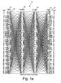
- FIG. 1a is a graphic representation of an illustrative embodiment of a four-stage fabric switch or network 10 which may be used in a network node such as an IP router.
- the network 10 is representative of switching elements in a data communications network, such as, for example, an ATM network or router.
- the interconnection network 10 can be thought of as a "switching networks" in function, and the terms shall be used interchangeably throughout.
- this exemplary network 10 comprises 64 ATM switching elements arranged in four columns. Each column contains 16 switching elements and represents one stage. There are four stages: A, B, C, and D.
- the first column 12 comprises 16 switch elements which represents a first stage or, in this example, stage A.
- the first switch element in the column 12 is labelled DPM #0.
- the second switch element in column 12 is labelled DPM #1.
- the third switch element in the column 12 is labelled DPM #2, etc.
- the last switch element in column 12 is labelled DPM #15.
- the second column 14 represents a first middle stage or stage B group of 16 switch elements which are also labelled DPM#0 through DPM#15.
- the third column 16 represents a second middle stage (stage C) group of 16 switch elements
- the fourth column 18 represents the last stage or stage D group of 16 switch elements.
- the ATM switching elements may be a data path controller (DPC).
- the main components of a switching element are a pair of elements called a data path (DP) and a DPC.
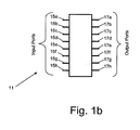
- FIG. 1b is a detailed illustration of an exemplary switching element, such as switching element 11. As illustrated, each switching element supports eight input ports 15a through 15h and eight output ports 17a through 17h, as shown in FIG. 1b . Packets encapsulated in an ATM cell form coming from an input port will exit the switching element via an output port. As discussed below, packets may enter the switch fabric via the input ports on column 12 which will be destined to one output port of column 18 (destination) via four DPCs (one DPC in each column or stage) of the 64 DPC shown in the switch fabric or network 10.
- DPCs one DPC in each column or stage
- interconnection switching network 10 consists of four stages A-D of 16 switching elements as shown in FIG. 1a .
- all switching elements with an even number DPC label in stage A e.g., DPC #0, 2, 4, 6, 8, 10, 12, 14
- DPC #0, 1, 2, 3, 4, 5, 6, and 7 in column 14 e.g., DPC #0, 1, 2, 3, 4, 5, 6, and 7 in column 14
- all switching elements with an odd number in stage A e.g., DPC#1, 3, 5, 7, 9, 11, 13, 15
- DPC# 8, 9, 10, 11, 12, 13, 14,15 in column 14 are connected to the bottom half of the sixteen switch elements in stage B (e.g., DPC# 8, 9, 10, 11, 12, 13, 14,15 in column 14).
- all switching elements with an even number DPC label in stage B are connected to the top half of the sixteen switch elements in stage C (e.g., DPC #0, 1, 2, 3, 4, 5, 6, and 7 in column 16).
- the switching elements with an odd number in stage B are connected to the bottom half of the sixteen switch elements in stage C (e.g., DPC# 8, 9, 10, 11, 12, 13, 14, 15 in column 16).
- the switching elements with an even numbers DPC label in stage C are connected to the top half of the sixteen switch elements in stage D (e.g., DPC #0, 1, 2, 3, 4, 5, 6, and 7 in column 18).
- the switching elements with an odd number in stage C are connected to the bottom half of the sixteen switch elements in stage D (e.g., DPC# 8, 9, 10, 11, 12, 13, 14, 15 in column 18).
- the collection of destination points of the interconnection network 10 is also referred to as the "egress" side of the interconnection network 10.
- DP and DPC pairs of stage A and last stage D, are on switching elements and stages B and C pairs are on the interconnection network 10.
- each DPC contains a virtual circuit identification (VCI) lookup table of size 8192 entries, or 1024 entries per input port for an 8-port board.
- FIG. 1c illustrates the architecture of such a VCI table in a DPC corresponding to the interconnection network 10 of FIG. 1a .
- a 13 bit index (0 to 8191) of the VCI table is a concatenation of a three bit internal port number (0 to 7) and a least significant ten bits of an incoming VCI number (0 to 1023). Therefore, at least 1024 VCIs may be supported for each input port 15a-15h as shown in FIG. 1b .
- 1024 (i.e., 8x128) entries may be enough for each DPC to support any combination of input ports (8 of them) and destination links (128 of links).
- Other VCI paths can be used for different QoS classes of traffic.
- VCIs can be supported for each input port.
- the ATM traffic cell coming from an input port of a DPC (with the input VCI of its ATM header) will be sent out on a new output port with replaced VCI value in its ATM header, based in part on the VCI lookup table for that DPC. That is, based on the VCI number of the ATM cell header, the input port number and the lookup table, the DPC can decide which static path pre-allocated will be used to deliver each traffic cell.
- the algorithms described later relates to setting up the VCI lookup table to allocate fully mesh VCI paths statically between any two input and output ports.
- FIGS. 1a and 1b The interconnection arrangement shown in FIGS. 1a and 1b is only an example and other interconnection configurations may be used.
- the even numbered switching elements of one stage may be linked to the bottom switching elements of the subsequent stage or the even number switching elements may be linked to only odd numbered switching elements of the subsequent stage.
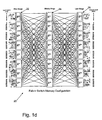
- Fig. 1d represents a graphic representation of another illustrative embodiment of a three-stage fabric switch or network 20 which may be used in a network node such as an IP router.
- the network 20 comprises 24 ATM switching elements arranged in three columns.
- the first column 22 of switch elements represents a first stage or, in this example, stage A.
- the second column 24 represents a middle stage or stage B.
- the third column 26 represents the last stage or stage C.
- FIGS. 1a , 1b , 1c and 1d are intended to be representative of the data routing systems in which the invention can be utilized and not a particular physical structure to which the invention is limited.
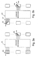
- FIG. 2 illustrates a path conflict within interconnection network 10 of FIGS. 1a , and 1b .
- a fundamental goal of VCI allocation is to ensure that there exists at least as many distinct paths from any one switching element in a first stage to any switching element in a last stage such that every input port of the switching element at a given slot in the interconnection network can reach any output port of the switching element at a given slot in the interconnection network. For example, as shown in FIGs.
- a data traffic pattern is a permutation of input ports to output ports between, for example, switching elements 202 and 204
- paths 206 and 208 may be used to transmit the data traffic at full speed.
- the data traffic may be transmitted in parallel if no other data traffic is being transmitted at the same time on a specific path.
- conflicts may occur when data traffic from input source ports, such as input ports 210 and 212, attempt to use the same physical path through switching element 214 to output destination ports, such as output ports 216 and 218.
- a conflict implies that data traffic inputs at ports 210 and 212 cannot use the same physical path simultaneously and maintain full bandwidth of the data routing system.
- the present invention provides a method and system of avoiding such conflicts while maintaining the bandwidth capabilities of the system used to route data.
- the method can be referred to as a VCI allocation algorithm while the system takes the form of a data routing system that includes the VCI allocation algorithm of the invention.
- FIGS. 3a through 3d illustrate different traffic pattern requirements in the example interconnection network where the switching elements can support both high speed and low speed ports.
- FIG. 3a graphically represents a two stage switch fabric or network 300. It can be seen that the VCI allocation algorithm supports a situation where a single output port on a high speed switching element 304 can provide the required speed to support a low speed multi-port switching element 302.
- a multi-port switching element 302 typically consists of two, four, six, or eight ports, although other configurations are possible. Therefore, traffic from the multiple ports of the low speed switching element 302 in the first stage may be aggregated into a single high speed switching 304 element in parallel without conflicts.
- FIG. 3b illustrates a situation which supports communications between high speed switching elements.
- traffic flows between the two high-speed interfaces boards 306 and 308 (with one port each).
- the traffic is split evenly into smaller stripes 307 and sent to multiple ports in the first stage.
- traffic can then be aggregated in the last stage to the desired output port 309.
- data traffic can then be aggregated in a last stage to a desired output port.
- traffic from high speed switching element 306 may be deaggregated for input into switching element 308.
- FIG. 3c illustrates the situation that a high-speed switching element can de-aggregate the input traffic from a single input port to different output ports of a low-speed egress switch element.
- FIG. 3d illustrates normal traffic between two low-speed boards with unique path.
- the different input ports on a switching element can communicate with different output ports of another switching element at full speed in parallel, as long as the combination pairs of input and output ports are different.
- interconnection network such as interconnection network 10
- Switching elements of differing speeds may be used and still avoid the problem of conflicts and congestion at certain points within the interconnection network experienced by prior art systems.
- the physical restrictions of the interconnection network and logical representations of the interconnection network are used to setup virtual channel identifiers that determine paths through the switching elements and links connecting the switching elements. These VCIs are used to evenly distribute data traffic throughout the interconnection network.
- the interconnection network may be made up of switching elements of varying speeds, which may include low speed switching elements and high speed switching elements.
- data traffic may be aggregated from multiple inputs into a single output.
- data traffic may be deaggregated from a single input into multiple outputs.
- data traffic may be striped.
- data traffic may be transmitted without any aggregation, deaggregation or striping involved.
- the networks and system support all these traffic patterns in order to balance traffic through the interconnection network.
- each switching element has an input side, and an output side and each side may contain a plurality of ports.
- the interconnection network is connected so that an output port of the switching element in a first stage is connected to an input port in a second stage.
- a link number which couples the switching elements may be represented by using, for example, seven bits.
- the first four bits of the seven bits may identify a number associated with a particular switching element and the three remaining bits may identify a port number for the switching element.
- an input source link number (consisting of the input switching element and the port of the switching element) may be designated with, for example, seven bits
- the output destination link number consististing of the output switching element and the port of the switching element
- a VCI mapping entry at a specific stage may be represented by:
- the architecture of the interconnection network may include some guidelines on the virtual circuit identifier allocation algorithm. Recall in the discussion referring to FIG. 1 a and 1b, the even switching elements of each stage are connected to the top half of the switching elements in the next stage and the odd switching elements of each stage are connected to the bottom half of the switching elements in the next stage. Therefore, in this example, some preliminary guidelines may be needed to evenly distribute the data traffic across the interconnection network.
- these guidelines may include the following:
- an even/odd bit of a switching element number associated with switching element in stage A equals a top/bottom bit of a switching element number associated with switching element in stage B.
- the remaining bits in the switching element number associated with switching element 11 in stage A equals the bits of an input port number associated with switching element 118 in stage B.
- the bits of the output port of switching element 11 in stage A equals the remaining bits of the switching element number associated with switching element 118 stage B.
- the output VCI number for switching element 11 in stage A equals the input VCI number of switching element 118 in stage B.
- FIG. 4 there is illustrated an exemplary flowchart illustrating a method of multi-stage VCI setup.
- the operation begins by setting up the interconnection network virtual circuit identifier (step 402). Then the middle stages of the interconnection network are identified in which a virtual circuit identifier is established (step 404). The switching element interconnection virtual circuit identifier is then set up (step 406). The first stage of the interconnection network is identified in which a virtual circuit identifier is established (step 408) and a last stage of the interconnection network is identified in which a virtual circuit identifier is established (step 410).
- FIG. 5 is an exemplary flowchart illustrating the method of virtual circuit identifier set up for a middle stage.
- the method of FIG. 5 is a further illustration of step 404 in FIG. 4 .
- the operation starts by identifying a middle stage switching element in the interconnection network (step 502).
- An input link coupled to a port in the middle stage switching element is identified (step 504).
- an output link coupled to the port in the middle stage switching element is identified (step 506).
- a path is selected for the output of the middle stage switching element (step 508).
- a VCI table entry for an input port and an output port for the middle stage switching element is setup (step 510).
- a VCI input number of an input port associated with the middle stage switching element is assigned (step 512).
- step 516 If another port is not associated with the middle stage switching element in which a VCI number needs to be assigned (step 516: NO), a determination is then made as to whether or not there is another middle stage in the interconnection network that has not yet been identified (step 518). If there is not another middle stage in the interconnection network that has not been identified (step 518: NO), the operation terminates. If there is another middle stage in the interconnection network that has not been identified (step 518: YES), the operation returns to step 502 in which a middle stage of the interconnection network is identified.
- FIG. 6 is an exemplary flowchart illustrating a method for virtual circuit identifier set up for a first stage.
- FIG. 6 is a further illustration of step 406 of FIG. 4 .
- the operation starts by identifying a first stage switching element in the interconnection network (step 602).
- An input port on the switching element for the first stage is identified (step 604).
- an output link coupled to input port on the switching element for the first stage is identified (step 606).
- a determination is then made as to whether the first stage switching element is a high speed switching element (step 608). If the first stage switching element is a high speed switching element (step 608: YES), a path is selected based on output port parameters (step 610). If the first stage switching element is not a high speed switching element (step 608: NO), the path is selected based on input port parameters (step 612).
- the operation then sets up a VCI table entry for an input port and an output port for the first stage switching element (step 614).
- a VCI input number is assigned for the input port in the VCI table (step 616).
- a VCI output number is assigned for the output port in the VCI table (step 618).
- a determination is then made as to whether or not there is another port on the first stage switching element that has not been identified (step 620). If there is not another port on the first stage switching element that has not been identified (step 620: NO), a determination is made as to whether or not there are any more switching elements in the first stage that have not been identified (step 622).
- step 622 If there are no more switching elements in the first stage that have not been identified (step 622: NO), the operation terminates. If there is another switching element in the first stage that has not been identified (step 622: YES), the operation returns to step 602 in which an input switching element is identified for the first stage. Returning to step 620, if there is another port on the first stage that has not been identified (step 620: YES), the operation returns to step 604 in which an input port on the first stage switching element is identified.
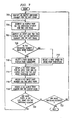
- FIG. 7 is an exemplary flowchart illustrating a method for last stage virtual circuit identifier setup.
- FIG. 7 is a further illustration of step 408 in FIG. 4 .
- the operation starts by identifying a last stage switching element on the interconnection network (step 702).
- An output port on the last stage switching element is then identified (step 704).
- An input link coupled to the output port on the last stage switching element is identified (step 706).
- a determination is then made as to whether or not the output switching element is a high speed switching element (step 708). If the output switching element is a high speed switching element (step 708: YES), a path is selected based on output port parameters (step 710). If the output switching element is not a high speed switching element (step 708: NO), the path is selected based on input port parameters (step 712).
- the operation then sets up a VCI table entry for the last stage switching element (step 714).
- a VCI input port number is assigned for the input port (step 716).
- a VCI output port number is assigned for the output port (step 718).
- a determination is then made as to whether or not another port remains on the last stage switching element which has not been identified (step 720). If another port does not remain on the last stage switching element which has not been identified (step 720: NO), a determination is made as to whether or not there are any more switching elements on the last stage which have not been identified (step 722). If there are not any more switching elements on the last stage which have not been identified (step 722: NO), the operation terminates.
- step 722 If there are more switching elements on the last stage which have not been identified (step 722: YES), the operation returns to step 702 in which an output switching element is identified for the last stage. Returning to step 720, if there is another port on the last stage switching element which has not been identified (step 720: YES), the operation returns to step 704 in which an output port on the last stage switching element is identified.
- FIG. 8 is an exemplary flowchart illustrating the method for a VCI allocation scheme that supports different traffic pattern requirements.
- the operation starts with analyzing physical restrictions and layout analysis of the interconnection network (step 802).
- the layout analysis of the interconnection network such as interconnection network 10 may include determining the number of switching elements and the number of links coupled to the switching elements.
- the physical restrictions are used to arrive at a logical representation of the architecture of the interconnection network.
- a traffic pattern requirement analysis is carried out (step 804). This traffic pattern analysis is used to balance the data traffic through the links coupling the switching elements.
- a bit representation and permutation functions are then translated which may dynamically calculate a specific VCI table entry of each switch element for a given source and destination link number in the interconnection network (step 806).
- the bit representation and permutation function may be a logical representation of the architecture of the interconnection network.
- a determination is made as to whether or not the different traffic requirements are verified (step 808). If the different traffic requirements are not verified (step 808: NO), the operation returns to step 806 in which a bit representation and permutation functions are translated. If the different traffic requirements are verified (step 808: YES), a switch element VCI is setup in the interconnection network (step 810) and thereafter the operation terminates.
- the logical representation and the traffic patterns of the interconnection network are used to setup virtual channel identifiers that determine the paths through which the data is routed. The data is routed through the switching elements and the links so that the data traffic is more evenly distributed through the interconnection network.
- Hot-swapping of switching elements is enabled and many features of different traffic patterns are satisfied.
- Hot-swapping of switching elements provides that a specific switching element may be replaced by another switching element without powering down the board to which the parts are connected or disturbing data traffic flow.
- the hot-swapping of switching elements is enabled without causing any interruption in the traffic patterns.
- a source link number may be preserved throughout transmission of the data to the destination port. Preservation of the source link number is desired because the destination link is able to determine the source of the traffic in an easy and efficient manner.
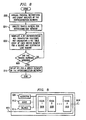
- FIG. 9 is an exemplary block diagram showing the use of the present invention within a switching network 900.
- Switching network 900 may include input 902, virtual circuit identification algorithm 904, stage 1 906, stage 2 908, stage n 910 and output 916.
- switching network 900 is a system for routing data.
- Switching network 900 consists of a plurality of switching elements within each stage 906-910 and a plurality of links coupling both the switching elements and the stages for providing a path for routing data.
- Virtual circuit identification algorithm 904 is in communication with switching network 900 and provides instructions for establishing an even distribution of data traffic through switching network 900.
- Switching network 900 includes logic 912 for determining the physical restrictions of the network 900.
- switching network 900 also includes logic 914 for balancing data traffic through the plurality of links using traffic patterns of the switching network 900.
- the present invention provides a method and system in which traffic between a source link and a destination link is evenly transmitted between stages in the interconnection network so that no conflict arises between the transmission of data.
- no available pathway in the interconnection network is wasted.
- Data traffic is transmitted evenly along the interconnection network so that one data path does not interfere with transmission of data on another data path.
- switching elements of various speeds may be used and the data traffic aggregated or deaggregated according to the speed requirements of the switching elements.
- the present invention provides for a systematic and orderly allocation of data traffic without conflicts and congestion in the interconnection network.
- the present invention provides an enhancement such that no contention should happen on the bidirectional traffic path between any two ports through the switch fabric to provide full-duplex performance on the interfaces. This applies to Low Speed to Low Speed, Low Speed to High Speed, and all 8 paths between High Speed to High Speed.
- First stage VCI assignment of High Speed ports needs to be independent to Egress slot number, to fulfill the "load balance on stripes" implementation on High-speed boards.
- bits j3-j6, as described herein below cannot be used in deciding the value of ⁇ a>, ⁇ b>, and ⁇ c> for HS paths, as in previous solutions.
- VCI paths can be used in fully duplex performance.
- traffic should be balanced among all possible paths to guarantee all DPCs have equal opportunity to be utilized.
- This invention also realizes the bit representation and the path selection formula for the 3-stage switch fabric.
- bit representation for the 4-stage switch fabric may be summarized as,
- the last 3 bits of VCI numbers are j[2,1,0] except the output VCI in the last stage, which is using i[2,1,0]. So, given an output slot (for a destination port) the VCI number of the traffic for that output slot will be different from the traffic to the other output slots.
- the output VCI number in the last stage is i, the source link number, which allows the last stage to determine which is the source link of the traffic.
- a 4-stage switch fabric (with First stage, Middle stage1, Middle stage2, Last stage) contains 128 links (numbered 0 ⁇ 127).
- There are 64 DPCs i.e., ATM switch). Packets encapsulated in an ATM cell form coming from one input link (source) will be designated to one output link (destination) via 4 DPCs of the 64 DPCs in the switch fabric.
- each packet Before being sent into the fabric, each packet may be encapsulated into a fabric ATM cell format (with proper padding and fragmentation.)
- a fabric ATM cell is similar to an ATM cell (e.g., it may have a 4-byte header and 48-byte payload).
- An exemplary 4-byte header is illustrated in Fig. 10 . As illustrated in Fig. 10 , the first four bits represents the gfc, the next 5 bits holds the vpi, and the following 11 bits holds the vci. The following four bits hold the oam, efci, eom, and clp bits respectively.
- the VCI field will be used to forward the traffic inside the router fabric based on the VCI value.
- This VCI field may be used by each fabric stage to decide where (e.g., which DPC output port) to send the cell next.
- each physical link in this illustrative example could carry 16-bit (2 ⁇ 16) VCI numbers, this discussion will use 7-bit VCI numbers for the sake of simplicity.
- the DPC When a packet cell reaches the DPC of each stage, the DPC will perform a table lookup (on its pre-populated switch table), based on the input port number and the input VCI number of this packet, to decide which output port to direct this packet cell to the next stage DPC, and which new output VCI to put on the packet cell header for the next stage DPC.
- the DPC number (0 ⁇ 15, i.e., slot number) and the port number (0 ⁇ 7) on a specific DPC can be derived from a link number (0 ⁇ 127).
- the packet may carry the output link j (destination) as its input vci number in its ATM header so its destination may be determined.
- the traverse packet In the Last Stage DPC, the traverse packet carries the input link i (source) as its output VCI number, so that its source may be determined.
- Fig. 11 there is presented a First-stage and Last stage DPC setup for populating a VCI table which may be used in an exemplary four stage switch fabric, such as one illustrated in Fig. 1a .
- the Middle stage DPC setup will be discussed in reference to Fig. 12 .
- the discussion will use a 7-bit link number (0 ⁇ 127) to represent the input (src) and output (dst) links.
- the DPC paths setup are for the traffic sent from link i[6,5,4,3,2,1,0] to output link j[6,5,4,3,2,1,0]. Under this scenario, there are 128x128 possible combinations of the input and output links.
- FIG. 11 therefore, illustrates an exemplary process which calculates the VCI entries and populates the table entries (i.e., 128x128 entries in each DPC) for the First and Last stage DPCs.
- the various table entries are populated using a series of nested loops.
- Step 1102 represents the start of a first loop (or loop i) which performs a process to populate a table for each DPC in the first and last stages (i.e., with slot number 0 ⁇ 15).
- Step 1104 represents the start of a nested loop which performs a process on each input port number (0 ⁇ 7).
- step 1106 represents the start of a nested loop which performs a process on each output link number (0 ⁇ 127).
- step 1108 the process determines if the DPC in question is on a high speed board that performs traffic stripping. If no, then the process flows to step 1110. On the other hand, if the DPC in question is on a high speed board that performs traffic stripping, then the process flows to step 1112. Steps 1110 and 1112 calculate the path selection value (a, b, c, d, e), where a, b, c, d, and e are only binary bit (0 or 1). The path selection value (a, b, c, d, e) also decide which DPCs to use during the virtual circuit path from the First Stage input to the Last Stage output.
- Step 1110 calculates the path selection formula for a normal board.
- the first stage DPC output port number i.e., a, b, c
- the first stage DPC output port number is chosen by the value of the input port number (i[2] , i[1], i[0]) exclusive OR on the 3 bits of the Last Stage output DPC slot number (j[5], j[4], j[3]) and one bit of the input DPC slot number (i[6]).
- (c, d, e) which decides the Middle stage DPC output port (and which DPC) and also the Last stage DPC input port number is chosen by the exclusive OR on the First Stage DPC input port number reversed (i[0], i[1], i[2]) with the partial input DPC slot number bits (i[6], i[4], i[5]) and the Last Stage output DPC slot number bits (j[3], j[4], j[5]).
- the path selection formula would then be:
- Step 1112 calculates the path selection formula for a high speed board with stripping.
- the Last Stage output DPC port number can be used to decide (a, b, c); and (c, d, e) is exclusive OR on the Last stage DPC output port number reversed (j[0], j[1], j[2]) with the partial of input DPC slot number (i[4], i[5]).
- the table entry values on the given First Stage DPC number may then be determined and populated in step 1114.
- the input port value for a given First Stage DPC number may be determined by:
- the output port value may for a given First Stage DPC number be calculated as:
- step 1116 the table entry values on the given Last Stage DPC number may then be determined and populated.
- the input port for a given Last Stage DPC number may be determined by:
- the output port may for a given Last Stage DPC number be calculated as:
- Step 1118 signals the end of the loop which began in step 1106.
- step 1120 represents the end of the loop which began in step 1102.
- FIG. 12 illustrates an exemplary process which calculates the VCI entries and populates the table entries (i.e., 128x128 entries in each DPC) for the first and second middle stage DPCs.
- the various table entries are populated using a series of nested loops.
- Step 1202 represents the start of a first loop (or loop i) which performs a process to populate a table for each DPC in the first and last stages (i.e., with slot number 0-15).
- Step 1204 represents the start of a nested loop which performs a process on each input port number (0 ⁇ 7).
- step 1206 represents the start of a nested loop which performs a process on each output link number (0-127).
- step 1208 the process determines if the DPC in question is on a high speed board that performs traffic stripping. If no, then the process flows to step 1210. On the other hand, if the DPC in question is on a high speed board that performs traffic stripping, then the process flows to step 1212. Steps 1210 and 1212 calculate the path selection value (a, b, c, d, e), where a, b, c, d, and e are only binary bit (0 or 1).
- step 1210 the path selection formula is calculated using the path selection formula for a normal board as previously described in reference to step 1110 of the process illustrated FIG. 11 . So, the path selection formula would then be:
- step 1212 calculates the path selection formula for a high speed board with stripping as described previously in reference to step 1110. So, the path selection formula would then be:
- the table entry values on the given first Middle Stage DPC number may then be determined and populated in step 1214.
- the output port may for a given First Stage DPC number be calculated as:
- step 1216 the table entry values on the given second Middle Stage DPC number may then be determined and populated.
- the input port for a given second Middle stage DPC number may be determined by:
- the output port may for a given Last Stage DPC number be calculated as:
- Step 1218 signals the end of the loop which began in step 1206.
- step 1220 represents the end of the loop which began in step 1202.
- the output port number of the first stage DPC is used to determine the DPC number of the second stage, and only (a, b, c) are used to select the physical paths.
- the bit representation may then be:
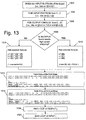
- FIG. 13 there is presented a First-stage and Last stage DPC setup for a three stage switch fabric.
- the Middle stage DPC setup will be discussed in reference to FIG. 14 .
- the discussion will use a 6-bit link number to represent the input (src) and output (dst) links or ports.
- the DPC paths setup are for the traffic sent from i[5,4,3,2,1,0] to output link j[5,4,3,2,1,0]. Under this scenario, there are 64*64 possible combinations of the input and output ports.
- FIG. 13 therefore, illustrates an exemplary process which calculates the VCI entries and populates the table entries (i.e., 64x64 entries in each DPC) for the First and Last stage DPCs.
- the various table entries are populated using a series of nested loops.
- Step 1302 represents the start of a first loop (or loop i) which performs a process to populate a table for each DPC in the first and last stages (i.e., with slot number 0-15).
- Step 1304 represents the start of a nested loop which performs a process on each input port number (0 ⁇ 7).
- step 1306 represents the start of a nested loop which performs a process on each output link number (0 ⁇ 64).
- step 1308 the process determines if the DPC in question is on a high speed board that performs traffic stripping. If no, then the process flows to step 1310. On the other hand, if the DPC in question is on a high speed board that performs traffic stripping, then the process flows to step 1312. Steps 1310 and 1312 calculate the path selection value (a, b, c).
- Step 1310 calculates the path selection formula for a normal board. Because any First Stage DPC can physically reach any Middle Stage DPC, we may have to increase the permutation distribution by using the exclusive OR on the input port number (i[2], i[1], i[0]) with all the input and output slot numbers(i[5, 4, 3] and j[5, 4, 3]). That is, the path selection formula would then be:
- Step 1312 calculates the path selection formula for a high-speed board with stripping.
- the Last Stage output port number can be used to decide (a, b, c) which is the First Stage output port (and thus also determine the Middle Stage DPC).
- the path selection formula would then be:
- the table entry values on the given First Stage DPC number may then be determined and populated in step 1314.
- the input port for a given First Stage DPC number may be determined by:
- the output port may for a given First Stage DPC number be calculated as:
- step 1316 the table entry values on the given Last Stage DPC number may then be determined and populated.
- the input port for a given Last Stage DPC number may be determined by:
- the output port may for a given Last Stage DPC number be calculated as:
- Step 1318 signals the end of the loop which began in step 1306.
- step 1320 represents the end of the loop which began in step 1302.
- FIG. 14 illustrates an exemplary process which calculates the VCI entries and populates the table entries (i.e., 64x64 entries in each DPC) for the middle stage DPCs of the exemplary 3-stage fabric switch.
- the various table entries are populated using a series of nested loops.
- Step 1402 represents the start of a first loop (or loop i) which performs the process for each DPC in the middle stage (i.e., with slot number 0 ⁇ 15).
- Step 1404 represents the start of a nested loop which performs a process on each input port number (0 ⁇ 7).
- step 1406 represents the start of a nested loop which performs a process on each output link number (0 ⁇ 63).
- step 1408 the process determines if the DPC in question is on a high speed board that performs traffic stripping. If no, then the process flows to step 1410. On the other hand, if the DPC in question is on a high speed board that performs traffic stripping, then the process flows to step 1412. Steps 1410 and 1412 calculate the path selection value (a, b, c).
- Step 1410 calculates the table entries at the Middle Stage DPCs of a normal board by using the same path selection formula as in Step 1310 so that the DPC setup in these three stage elements can be matched and form good VCI paths.
- the path selection formula would then be:
- Step 1412 similarly, calculates the table entries by using the same path selection formula as in Step 1312 for a high-speed board with stripping.
- the path selection formula would then be:
- the table entry values on the given Middle Stage DPC number may then be determined and populated in step 1415.
- the input port for a given Middle Stage DPC number may be determined by:
- Step 1416 signals the end of the loop which began in step 1406.
- step 1418 represents the end of the loop which began in step 1402.
Landscapes
- Engineering & Computer Science (AREA)
- Computer Networks & Wireless Communication (AREA)
- Signal Processing (AREA)
- Data Exchanges In Wide-Area Networks (AREA)
Claims (16)
- Procédé d'attribution de trajets au travers d'un réseau d'interconnexion (10 ; 20 ; 900) consistant en une pluralité d'éléments de commutation (11 ; 13 ; 302 ; 304 ; 306 ; 308), disposés en rangées et en colonnes (12 ; 14 ; 16 ; 18 ; 22 ; 24 ; 26), chaque colonne représentant un étage (906 ; 908 ; 910) du réseau d'interconnexion, et en une pluralité de liaisons qui couplent les éléments de commutation, dans lequel chacun des éléments de commutation est conçu pour recevoir un paquet de données et comprend un contrôleur de trajets de données, ledit contrôleur de trajets de données étant désigné par un numéro de case et ayant une table d'identificateurs de circuits virtuels, le procédé comprenant les étapes consistant à :utiliser des restrictions physiques du réseau d'interconnexion (10 ; 20 ; 900) pour parvenir à une représentation logique d'une architecture du réseau d'interconnexion ;déterminer des motifs de trafic du réseau d'interconnexion (10 ; 20 ; 900) pour équilibrer le trafic de données sur les liaisons qui couplent les éléments de commutation (11 ; 13 ; 302 ; 304 ; 306 ; 308) ; etétablir dans un contrôleur de trajets de données du premier étage (906) une table d'identificateurs de trajets virtuels qui représente des formules de sélection de trajets, en utilisant la représentation logique et les motifs de trafic du réseau d'interconnexion (10 ; 20 ; 900) ; etdéterminer, sur la base d'informations de l'en-tête des paquets, si le contrôleur de trajets de données qui va utiliser la table d'identificateurs de circuits virtuels se situe sur une carte à grande vitesse (304 ; 306 ; 308) qui pratique la répartition du trafic ou sur une carte à faible vitesse (302) ;caractérisé en ce que :l'établissement de la table d'identificateurs de circuits virtuels, dans le contrôleur de trajets de données du premier étage (906), est indépendant du numéro de case d'un contrôleur de trajets de données du dernier étage (910) s'il a été déterminé que le contrôleur de trajets de données qui utilisera la table d'identificateurs de circuits virtuels se situe sur une carte à grande vitesse (304 ; 306 ; 308) qui pratique la répartition du trafic, si bien que le trafic de données en duplex peut être distribué plus régulièrement sur le réseau d'interconnexion.
- Procédé selon la revendication 1, dans lequel l'augmentation du nombre des rangées et des colonnes (12 ; 14 ; 16 ; 18 ; 22 ; 24 ; 26) permet l'extensibilité du procédé.
- Procédé selon la revendication 1, dans lequel le nombre des étages est de quatre dans le réseau d'interconnexion (10).
- Procédé selon la revendication 3, dans lequel, si le contrôleur de trajets de données ne se situe pas sur une carte à grande vitesse (304 ; 306 ; 308) qui pratique la répartition du trafic, la formule de sélection du trajet est la suivante :a = i[2] ^ j[5]b = i[1] ^ j[4]c = i[0] ^ j[3] ^ i[6]d = i[1] ^ j[4] ^ i[4]e = i[2] ^ j[5] ^ i[5]oùi[n] est le nième bit d'une liaison d'entrée numéro i qui représente une liaison d'entrée d'un élément de commutation du premier étage (11) et j[m] est le mième bit d'une liaison de sortie numéro j représentant une liaison de sortie d'un élément de commutation du dernier étage (13),
^ est l'opération OU exclusif, eta, b, c, d et e sont des valeurs de sélection de trajet, a, b, c, d et e étant uniquement un bit binaire (0 ou 1) . - Procédé selon la revendication 3, dans lequel, si le contrôleur de trajets de données se situe sur une carte à grande vitesse (304 ; 306 ; 308) qui pratique la répartition du trafic, la formule de sélection du trajet est la suivante :a = j[2]b = j[1]c = j[0]d = j[1] ^ i[4]e = j[2] ^ i[5]oùi[n] est le nième bit d'une liaison d'entrée numéro i qui représente une liaison d'entrée d'un élément de commutation du premier étage (11) et [m] est le mième bit d'une liaison de sortie numéro j représentant une liaison de sortie d'un élément de commutation du dernier étage (13),i[2,1,0] = <0,0,0> eta, b, c, d et e sont des valeurs de sélection de trajet, a, b, c, d et e étant uniquement un bit binaire (0 ou 1) .
- Procédé selon la revendication 1, dans lequel le nombre d'étages est de trois dans le réseau d'interconnexion (20).
- Procédé selon la revendication 6, dans lequel, si le contrôleur de trajets de données n'est pas situé sur une carte à grande vitesse (304 ; 306 ; 308) qui pratique la répartition du trafic, la formule de sélection du trajet est la suivante :a = i[2] ^ ji[5]b = i[1] ^ j[4] ^ i[4]c = i[0] ^ j[5] ^ i[3]oùi[n] est le nième bit d'une liaison d'entrée numéro i qui représente une liaison d'entrée d'un élément de commutation du premier étage (22) et j[m] est le mième bit d'une liaison de sortie numéro j représentant une liaison de sortie d'un élément de commutation du dernier étage (26),
^ est l'opération OU exclusif, eta, b et c sont des valeurs de sélection de trajet, a, b et c étant uniquement un bit binaire (0 ou 1). - Procédé selon la revendication 6, dans lequel, si le contrôleur de trajets de données est situé sur une carte à grande vitesse (304 ; 306 ; 308) qui pratique la répartition du trafic, la formule de sélection du trajet est la suivante :a = j[2]b = j[1]c = j[0]oùi[n] est le nième bit d'une liaison d'entrée numéro i qui représente une liaison d'entrée d'un élément de commutation du premier étage (22) et j[m] est le mième bit d'une liaison de sortie numéro j représentant une liaison de sortie d'un élément de commutation du dernier étage (26),i[2,1,0] = <0, 0, 0> et
a, b et c sont des valeurs de sélection de trajet, a, b et c étant uniquement un bit binaire (0 ou 1). - Système destiné à router des données, comprenant :un noeud de commutation (10 ; 20 ; 900), comprenant une pluralité d'éléments de commutation (11 ; 13 ; 302 ; 304 ; 306 ; 308), disposés en rangées et en colonnes (12 ; 14 ; 16 ; 18 ; 22 ; 24 ; 26), chaque colonne représentant un étage (906 ; 908 ; 910) du réseau d'interconnexion, et une pluralité de liaisons couplées aux éléments de commutation afin de fournir un trajet de routage pour les données, dans lequel chacun des éléments de commutation est conçu pour recevoir un paquet de données et comprend un contrôleur de trajets de données, ledit contrôleur de trajets de données étant désigné par un numéro de case et ayant une table d'identificateurs de circuits virtuels ;un moyen (912), destiné à déterminer, sur la base d'informations de l'en-tête des paquets, si le contrôleur de trajets de données qui va utiliser la table d'identificateurs de circuits virtuels se situe sur une carte à grande vitesse (304 ; 306 ; 308) qui pratique la répartition du trafic ou sur une carte à faible vitesse (302) ; etun moyen d'identification de circuit virtuel (904), en communication avec le réseau d'interconnexion (10 ; 20 ; 900) afin d'assurer une distribution régulière du trafic de données sur le noeud de commutation, le moyen d'identification de circuit virtuel (904) étant conçu pour déterminer une formule de sélection de trajet utilisée pour renseigner une table d'identificateurs de circuits virtuels ;caractérisé en ce que :le moyen d'identification de circuit virtuel (904) est conçu pour établir la table d'identificateurs de circuits virtuels dans le contrôleur de trajets de données du premier étage (906) indépendamment du numéro de case d'un contrôleur de trajets de données du dernier étage (910) s'il a été déterminé que le contrôleur de trajets de données qui utilisera la table d'identificateurs de circuits virtuels se situe sur une carte à grande vitesse (304 ; 306 ; 308) qui pratique la répartition du trafic, si bien que le trafic de données en duplex peut être distribué plus régulièrement sur le noeud de commutation (10 ; 20 ; 900).
- Système selon la revendication 9, dans lequel l'augmentation du nombre des rangées et des colonnes (12 ; 14 ; 16 ; 18 ; 22 ; 24 ; 26) permet l'extensibilité du procédé.
- Système selon la revendication 9, dans lequel le nombre des étages est de quatre dans le noeud d'interconnexion (10).
- Système selon la revendication 11, dans lequel, si le contrôleur de trajets de données ne se situe pas sur une carte à grande vitesse (304 ; 306 ; 308) qui pratique la répartition du trafic, la formule de sélection du trajet est la suivante :a = i[2] ^ j[5]b = i[1] ^ j[4]c = i[0] ^ j[3] ^ i[6]d = i[1] ^ j[4] ^ i[4]e = i[2] ^ j[5] ^ i[5]oùi[n] est le nième bit d'une liaison d'entrée numéro i qui représente une liaison d'entrée d'un élément de commutation du premier étage (11) et j[m] est le mième bit d'une liaison de sortie numéro j représentant une liaison de sortie d'un élément de commutation du dernier étage (13),
^ est l'opération OU exclusif eta, b, c, d et e sont des valeurs de sélection de trajet, a, b, c, d et e étant uniquement un bit binaire (0 ou 1). - Système selon la revendication 11, dans lequel, si le contrôleur de trajets de données se situe sur une carte à grande vitesse (304 ; 306 ; 308) qui pratique la répartition du trafic, la formule de sélection du trajet est la suivante :a = j[2]b = j[1]c = j[0]d = j[1] ^ i[4]e = j[2] ^ i[5]oùi[n] est le nième bit d'une liaison d'entrée numéro i qui représente une liaison d'entrée d'un élément de commutation du premier étage (11) et j[m] est le mième bit d'une liaison de sortie numéro j représentant une liaison de sortie d'un élément de commutation du dernier étage (13),i [2, 1, 0] = <0, 0, 0> eta, b, c, d et e sont des valeurs de sélection de trajet, a, b, c, d et e étant uniquement un bit binaire (0 ou 1) .
- Système selon la revendication 9, dans lequel le nombre d'étages est de trois dans le noeud d'interconnexion (20).
- Système selon la revendication 14, dans lequel, si le contrôleur de trajets de données n'est pas situé sur une carte à grande vitesse (304 ; 306 ; 308) qui pratique la répartition du trafic, la formule de sélection du trajet est la suivante :a = i [2] ^ j [5] ^ i [5]b = i [1] ^ j [4] ^ i [4]c = i [0] ^ j [5] ^ i [3]oùi [n] est le nième bit d'une liaison d'entrée numéro i qui représente une liaison d'entrée d'un élément de commutation du premier étage (22) et j [m] est le mième bit d'une liaison de sortie numéro j représentant une liaison de sortie d'un élément de commutation du dernier étage (26),
^ est l'opération OU exclusif eta, b et c sont des valeurs de sélection de trajet, a, b et c étant uniquement un bit binaire (0 ou 1). - Système selon la revendication 14, dans lequel, si le contrôleur de trajets de données est situé sur une carte à grande vitesse (304 ; 306 ; 308) qui pratique la répartition du trafic, la formule de sélection du trajet est la suivante :a = j [2]b = j [1]c = j [0]oùi[n] est le nième bit d'une liaison d'entrée numéro i qui représente une liaison d'entrée d'un élément de commutation du premier étage (22) et j [m] est le mième bit d'une liaison de sortie numéro j représentant une liaison de sortie d'un élément de commutation du dernier étage (26),i [2, 1, 0] = <0, 0, 0> eta, b et c sont des valeurs de sélection de trajet, a, b et c étant uniquement un bit binaire (0 ou 1).
Applications Claiming Priority (2)
| Application Number | Priority Date | Filing Date | Title |
|---|---|---|---|
| US11/182,242 US7515594B2 (en) | 2005-07-15 | 2005-07-15 | Enhanced virtual circuit allocation methods and systems for multi-stage switching elements |
| PCT/IB2006/001936 WO2007010351A1 (fr) | 2005-07-15 | 2006-07-13 | Procedes et systemes d'attribution de circuit virtuel ameliores pour des elements de commutation a etages multiples |
Publications (2)
| Publication Number | Publication Date |
|---|---|
| EP1908306A1 EP1908306A1 (fr) | 2008-04-09 |
| EP1908306B1 true EP1908306B1 (fr) | 2011-10-12 |
Family
ID=37265454
Family Applications (1)
| Application Number | Title | Priority Date | Filing Date |
|---|---|---|---|
| EP06795110A Not-in-force EP1908306B1 (fr) | 2005-07-15 | 2006-07-13 | Procedes et systemes d'attribution de circuit virtuel ameliores pour des elements de commutation a etages multiples |
Country Status (6)
| Country | Link |
|---|---|
| US (1) | US7515594B2 (fr) |
| EP (1) | EP1908306B1 (fr) |
| CN (1) | CN101268703B (fr) |
| AT (1) | ATE528927T1 (fr) |
| CA (1) | CA2620971C (fr) |
| WO (1) | WO2007010351A1 (fr) |
Families Citing this family (8)
| Publication number | Priority date | Publication date | Assignee | Title |
|---|---|---|---|---|
| US7596112B2 (en) * | 2005-03-22 | 2009-09-29 | Interdigital Technology Corporation | Method and apparatus for rate compatible dirty paper coding |
| US7944401B2 (en) | 2008-05-29 | 2011-05-17 | Kimberly-Clark Worldwide, Inc. | Radiating element for a signal emitting apparatus |
| US20100291649A1 (en) * | 2009-05-18 | 2010-11-18 | E. I. Du Pont De Nemours And Company | Control of contaminant yeast in fermentation processes |
| US9065773B2 (en) * | 2010-06-22 | 2015-06-23 | Juniper Networks, Inc. | Methods and apparatus for virtual channel flow control associated with a switch fabric |
| US8923277B1 (en) * | 2010-12-15 | 2014-12-30 | Juniper Networks, Inc. | Methods and apparatus related to flexible physical interface naming in a distributed switch fabric system |
| US8942232B1 (en) * | 2012-02-02 | 2015-01-27 | Google Inc. | Multi-stage switching topology |
| US11368336B2 (en) * | 2017-07-10 | 2022-06-21 | The Regents Of The University Of California | Method and apparatus for interfacing with a circuit switched network |
| US11074091B1 (en) * | 2018-09-27 | 2021-07-27 | Juniper Networks, Inc. | Deployment of microservices-based network controller |
Family Cites Families (8)
| Publication number | Priority date | Publication date | Assignee | Title |
|---|---|---|---|---|
| US6031840A (en) * | 1995-12-07 | 2000-02-29 | Sprint Communications Co. L.P. | Telecommunications system |
| US5872918A (en) * | 1995-07-14 | 1999-02-16 | Telefonaktiebolaget Lm Erisson (Publ) | System and method for optimal virtual path capacity dimensioning with broadband traffic |
| US5841775A (en) * | 1996-07-16 | 1998-11-24 | Huang; Alan | Scalable switching network |
| US6188690B1 (en) * | 1996-12-12 | 2001-02-13 | Pmc-Sierra, Inc. | Method and apparatus for high speed, scalable communication system |
| US6069895A (en) * | 1997-08-29 | 2000-05-30 | Nortel Networks Corporation | Distributed route server |
| US6606650B2 (en) * | 1999-08-30 | 2003-08-12 | Nortel Networks Limited | Bump in the wire transparent internet protocol |
| US20020075862A1 (en) * | 2000-12-20 | 2002-06-20 | Mayes Mark G. | Recursion based switch fabric for aggregate tipor |
| US7336658B2 (en) | 2001-02-28 | 2008-02-26 | Telefonaktiebolaget Lm Ericsson (Publ) | Methods and system of virtual circuit identification based on bit permutation of link numbers for multi-stage elements |
-
2005
- 2005-07-15 US US11/182,242 patent/US7515594B2/en active Active
-
2006
- 2006-07-13 CA CA2620971A patent/CA2620971C/fr not_active Expired - Fee Related
- 2006-07-13 EP EP06795110A patent/EP1908306B1/fr not_active Not-in-force
- 2006-07-13 CN CN2006800341796A patent/CN101268703B/zh not_active Expired - Fee Related
- 2006-07-13 WO PCT/IB2006/001936 patent/WO2007010351A1/fr not_active Ceased
- 2006-07-13 AT AT06795110T patent/ATE528927T1/de not_active IP Right Cessation
Also Published As
| Publication number | Publication date |
|---|---|
| WO2007010351A1 (fr) | 2007-01-25 |
| CN101268703A (zh) | 2008-09-17 |
| CN101268703B (zh) | 2011-12-14 |
| EP1908306A1 (fr) | 2008-04-09 |
| US7515594B2 (en) | 2009-04-07 |
| CA2620971A1 (fr) | 2007-01-25 |
| ATE528927T1 (de) | 2011-10-15 |
| US20070014299A1 (en) | 2007-01-18 |
| CA2620971C (fr) | 2013-05-28 |
Similar Documents
| Publication | Publication Date | Title |
|---|---|---|
| KR100194813B1 (ko) | 멀티채널/멀티캐스트 스위칭 기능을 갖는 패킷 스위칭장치 및 이를 이용한 패킷 스위칭 시스템 | |
| US5467349A (en) | Address handler for an asynchronous transfer mode switch | |
| US6157643A (en) | Switching fabric | |
| US5987028A (en) | Multiple channel ATM switch | |
| CA2074346C (fr) | Systeme de telecommunication | |
| US5504743A (en) | Message routing | |
| US5940389A (en) | Enhanced partially self-routing algorithm for controller Benes networks | |
| US7212528B2 (en) | System and method for reassembling packets in a network element | |
| EP1908306B1 (fr) | Procedes et systemes d'attribution de circuit virtuel ameliores pour des elements de commutation a etages multiples | |
| US6359885B1 (en) | Multi-channel packet switching apparatus having traffic flow controlling and checking functions | |
| US7512134B2 (en) | System and method for transmitting data packets in an infiniband network | |
| US7336658B2 (en) | Methods and system of virtual circuit identification based on bit permutation of link numbers for multi-stage elements | |
| US6289019B1 (en) | Device and method for switching ATM cells to groups of connections and corresponding input and output terminal functions | |
| AU670662B2 (en) | A telecommunications system and a method of transmitting data in a telecommunications system | |
| US6700896B1 (en) | High-capacity WDM data network | |
| US7924847B1 (en) | Method and system for virtual circuit numbering | |
| EP1326384B1 (fr) | Technique pour le calcul de chemins dans un commutateur de réseau multi-étages par l'exploitation de liaisons symétrique | |
| US20030095308A1 (en) | Method and apparatus of determining loss characteristics in DWDM links | |
| JP3014619B2 (ja) | 非同期転送モード通信システムおよびそのセル分解装置ならびに非同期転送モード通信方式 | |
| EP1158734A2 (fr) | Procédé d'allocation de circuits logiques à circuits logiques | |
| US20030028874A1 (en) | Channel set system and switching device | |
| WO2006035202A1 (fr) | Attribution de canaux destinee a un agencement de commutateurs a etages multiples | |
| US20010005380A1 (en) | Network node for switching digital information of different protocol types | |
| EP1317808A1 (fr) | Procede et dispositif pour former des flux de donnees |
Legal Events
| Date | Code | Title | Description |
|---|---|---|---|
| PUAI | Public reference made under article 153(3) epc to a published international application that has entered the european phase |
Free format text: ORIGINAL CODE: 0009012 |
|
| 17P | Request for examination filed |
Effective date: 20080117 |
|
| AK | Designated contracting states |
Kind code of ref document: A1 Designated state(s): AT BE BG CH CY CZ DE DK EE ES FI FR GB GR HU IE IS IT LI LT LU LV MC NL PL PT RO SE SI SK TR |
|
| 17Q | First examination report despatched |
Effective date: 20090617 |
|
| GRAP | Despatch of communication of intention to grant a patent |
Free format text: ORIGINAL CODE: EPIDOSNIGR1 |
|
| DAX | Request for extension of the european patent (deleted) | ||
| GRAS | Grant fee paid |
Free format text: ORIGINAL CODE: EPIDOSNIGR3 |
|
| GRAA | (expected) grant |
Free format text: ORIGINAL CODE: 0009210 |
|
| AK | Designated contracting states |
Kind code of ref document: B1 Designated state(s): AT BE BG CH CY CZ DE DK EE ES FI FR GB GR HU IE IS IT LI LT LU LV MC NL PL PT RO SE SI SK TR |
|
| REG | Reference to a national code |
Ref country code: GB Ref legal event code: FG4D |
|
| REG | Reference to a national code |
Ref country code: CH Ref legal event code: EP |
|
| REG | Reference to a national code |
Ref country code: IE Ref legal event code: FG4D |
|
| REG | Reference to a national code |
Ref country code: DE Ref legal event code: R096 Ref document number: 602006025076 Country of ref document: DE Effective date: 20111215 |
|
| REG | Reference to a national code |
Ref country code: NL Ref legal event code: VDEP Effective date: 20111012 |
|
| LTIE | Lt: invalidation of european patent or patent extension |
Effective date: 20111012 |
|
| REG | Reference to a national code |
Ref country code: AT Ref legal event code: MK05 Ref document number: 528927 Country of ref document: AT Kind code of ref document: T Effective date: 20111012 |
|
| PG25 | Lapsed in a contracting state [announced via postgrant information from national office to epo] |
Ref country code: LT Free format text: LAPSE BECAUSE OF FAILURE TO SUBMIT A TRANSLATION OF THE DESCRIPTION OR TO PAY THE FEE WITHIN THE PRESCRIBED TIME-LIMIT Effective date: 20111012 Ref country code: BE Free format text: LAPSE BECAUSE OF FAILURE TO SUBMIT A TRANSLATION OF THE DESCRIPTION OR TO PAY THE FEE WITHIN THE PRESCRIBED TIME-LIMIT Effective date: 20111012 Ref country code: IS Free format text: LAPSE BECAUSE OF FAILURE TO SUBMIT A TRANSLATION OF THE DESCRIPTION OR TO PAY THE FEE WITHIN THE PRESCRIBED TIME-LIMIT Effective date: 20120212 |
|
| PG25 | Lapsed in a contracting state [announced via postgrant information from national office to epo] |
Ref country code: PT Free format text: LAPSE BECAUSE OF FAILURE TO SUBMIT A TRANSLATION OF THE DESCRIPTION OR TO PAY THE FEE WITHIN THE PRESCRIBED TIME-LIMIT Effective date: 20120213 Ref country code: SE Free format text: LAPSE BECAUSE OF FAILURE TO SUBMIT A TRANSLATION OF THE DESCRIPTION OR TO PAY THE FEE WITHIN THE PRESCRIBED TIME-LIMIT Effective date: 20111012 Ref country code: LV Free format text: LAPSE BECAUSE OF FAILURE TO SUBMIT A TRANSLATION OF THE DESCRIPTION OR TO PAY THE FEE WITHIN THE PRESCRIBED TIME-LIMIT Effective date: 20111012 Ref country code: NL Free format text: LAPSE BECAUSE OF FAILURE TO SUBMIT A TRANSLATION OF THE DESCRIPTION OR TO PAY THE FEE WITHIN THE PRESCRIBED TIME-LIMIT Effective date: 20111012 Ref country code: GR Free format text: LAPSE BECAUSE OF FAILURE TO SUBMIT A TRANSLATION OF THE DESCRIPTION OR TO PAY THE FEE WITHIN THE PRESCRIBED TIME-LIMIT Effective date: 20120113 Ref country code: SI Free format text: LAPSE BECAUSE OF FAILURE TO SUBMIT A TRANSLATION OF THE DESCRIPTION OR TO PAY THE FEE WITHIN THE PRESCRIBED TIME-LIMIT Effective date: 20111012 |
|
| PG25 | Lapsed in a contracting state [announced via postgrant information from national office to epo] |
Ref country code: CY Free format text: LAPSE BECAUSE OF FAILURE TO SUBMIT A TRANSLATION OF THE DESCRIPTION OR TO PAY THE FEE WITHIN THE PRESCRIBED TIME-LIMIT Effective date: 20111012 |
|
| PG25 | Lapsed in a contracting state [announced via postgrant information from national office to epo] |
Ref country code: CZ Free format text: LAPSE BECAUSE OF FAILURE TO SUBMIT A TRANSLATION OF THE DESCRIPTION OR TO PAY THE FEE WITHIN THE PRESCRIBED TIME-LIMIT Effective date: 20111012 Ref country code: EE Free format text: LAPSE BECAUSE OF FAILURE TO SUBMIT A TRANSLATION OF THE DESCRIPTION OR TO PAY THE FEE WITHIN THE PRESCRIBED TIME-LIMIT Effective date: 20111012 Ref country code: BG Free format text: LAPSE BECAUSE OF FAILURE TO SUBMIT A TRANSLATION OF THE DESCRIPTION OR TO PAY THE FEE WITHIN THE PRESCRIBED TIME-LIMIT Effective date: 20120112 Ref country code: SK Free format text: LAPSE BECAUSE OF FAILURE TO SUBMIT A TRANSLATION OF THE DESCRIPTION OR TO PAY THE FEE WITHIN THE PRESCRIBED TIME-LIMIT Effective date: 20111012 Ref country code: DK Free format text: LAPSE BECAUSE OF FAILURE TO SUBMIT A TRANSLATION OF THE DESCRIPTION OR TO PAY THE FEE WITHIN THE PRESCRIBED TIME-LIMIT Effective date: 20111012 |
|
| PLBE | No opposition filed within time limit |
Free format text: ORIGINAL CODE: 0009261 |
|
| STAA | Information on the status of an ep patent application or granted ep patent |
Free format text: STATUS: NO OPPOSITION FILED WITHIN TIME LIMIT |
|
| PG25 | Lapsed in a contracting state [announced via postgrant information from national office to epo] |
Ref country code: RO Free format text: LAPSE BECAUSE OF FAILURE TO SUBMIT A TRANSLATION OF THE DESCRIPTION OR TO PAY THE FEE WITHIN THE PRESCRIBED TIME-LIMIT Effective date: 20111012 Ref country code: IT Free format text: LAPSE BECAUSE OF FAILURE TO SUBMIT A TRANSLATION OF THE DESCRIPTION OR TO PAY THE FEE WITHIN THE PRESCRIBED TIME-LIMIT Effective date: 20111012 Ref country code: PL Free format text: LAPSE BECAUSE OF FAILURE TO SUBMIT A TRANSLATION OF THE DESCRIPTION OR TO PAY THE FEE WITHIN THE PRESCRIBED TIME-LIMIT Effective date: 20111012 |
|
| 26N | No opposition filed |
Effective date: 20120713 |
|
| REG | Reference to a national code |
Ref country code: DE Ref legal event code: R097 Ref document number: 602006025076 Country of ref document: DE Effective date: 20120713 |
|
| PG25 | Lapsed in a contracting state [announced via postgrant information from national office to epo] |
Ref country code: AT Free format text: LAPSE BECAUSE OF FAILURE TO SUBMIT A TRANSLATION OF THE DESCRIPTION OR TO PAY THE FEE WITHIN THE PRESCRIBED TIME-LIMIT Effective date: 20111012 |
|
| PG25 | Lapsed in a contracting state [announced via postgrant information from national office to epo] |
Ref country code: MC Free format text: LAPSE BECAUSE OF NON-PAYMENT OF DUE FEES Effective date: 20120731 |
|
| REG | Reference to a national code |
Ref country code: CH Ref legal event code: PL |
|
| PG25 | Lapsed in a contracting state [announced via postgrant information from national office to epo] |
Ref country code: CH Free format text: LAPSE BECAUSE OF NON-PAYMENT OF DUE FEES Effective date: 20120731 Ref country code: ES Free format text: LAPSE BECAUSE OF FAILURE TO SUBMIT A TRANSLATION OF THE DESCRIPTION OR TO PAY THE FEE WITHIN THE PRESCRIBED TIME-LIMIT Effective date: 20120123 Ref country code: LI Free format text: LAPSE BECAUSE OF NON-PAYMENT OF DUE FEES Effective date: 20120731 |
|
| REG | Reference to a national code |
Ref country code: IE Ref legal event code: MM4A |
|
| PG25 | Lapsed in a contracting state [announced via postgrant information from national office to epo] |
Ref country code: FI Free format text: LAPSE BECAUSE OF FAILURE TO SUBMIT A TRANSLATION OF THE DESCRIPTION OR TO PAY THE FEE WITHIN THE PRESCRIBED TIME-LIMIT Effective date: 20111012 |
|
| PG25 | Lapsed in a contracting state [announced via postgrant information from national office to epo] |
Ref country code: IE Free format text: LAPSE BECAUSE OF NON-PAYMENT OF DUE FEES Effective date: 20120713 |
|
| PG25 | Lapsed in a contracting state [announced via postgrant information from national office to epo] |
Ref country code: TR Free format text: LAPSE BECAUSE OF FAILURE TO SUBMIT A TRANSLATION OF THE DESCRIPTION OR TO PAY THE FEE WITHIN THE PRESCRIBED TIME-LIMIT Effective date: 20111012 |
|
| PG25 | Lapsed in a contracting state [announced via postgrant information from national office to epo] |
Ref country code: LU Free format text: LAPSE BECAUSE OF NON-PAYMENT OF DUE FEES Effective date: 20120713 |
|
| PG25 | Lapsed in a contracting state [announced via postgrant information from national office to epo] |
Ref country code: HU Free format text: LAPSE BECAUSE OF FAILURE TO SUBMIT A TRANSLATION OF THE DESCRIPTION OR TO PAY THE FEE WITHIN THE PRESCRIBED TIME-LIMIT Effective date: 20060713 |
|
| REG | Reference to a national code |
Ref country code: FR Ref legal event code: PLFP Year of fee payment: 11 |
|
| REG | Reference to a national code |
Ref country code: FR Ref legal event code: PLFP Year of fee payment: 12 |
|
| REG | Reference to a national code |
Ref country code: FR Ref legal event code: PLFP Year of fee payment: 13 |
|
| PGFP | Annual fee paid to national office [announced via postgrant information from national office to epo] |
Ref country code: DE Payment date: 20180727 Year of fee payment: 13 Ref country code: FR Payment date: 20180726 Year of fee payment: 13 |
|
| PGFP | Annual fee paid to national office [announced via postgrant information from national office to epo] |
Ref country code: GB Payment date: 20180727 Year of fee payment: 13 |
|
| REG | Reference to a national code |
Ref country code: DE Ref legal event code: R119 Ref document number: 602006025076 Country of ref document: DE |
|
| GBPC | Gb: european patent ceased through non-payment of renewal fee |
Effective date: 20190713 |
|
| PG25 | Lapsed in a contracting state [announced via postgrant information from national office to epo] |
Ref country code: GB Free format text: LAPSE BECAUSE OF NON-PAYMENT OF DUE FEES Effective date: 20190713 Ref country code: DE Free format text: LAPSE BECAUSE OF NON-PAYMENT OF DUE FEES Effective date: 20200201 |
|
| PG25 | Lapsed in a contracting state [announced via postgrant information from national office to epo] |
Ref country code: FR Free format text: LAPSE BECAUSE OF NON-PAYMENT OF DUE FEES Effective date: 20190731 |