EP1906257A2 - Substrate, method of exposing a subsrate, machine readable medium - Google Patents
Substrate, method of exposing a subsrate, machine readable medium Download PDFInfo
- Publication number
- EP1906257A2 EP1906257A2 EP06254878A EP06254878A EP1906257A2 EP 1906257 A2 EP1906257 A2 EP 1906257A2 EP 06254878 A EP06254878 A EP 06254878A EP 06254878 A EP06254878 A EP 06254878A EP 1906257 A2 EP1906257 A2 EP 1906257A2
- Authority
- EP
- European Patent Office
- Prior art keywords
- layer
- resist
- exposure
- radiation
- positive tone
- Prior art date
- Legal status (The legal status is an assumption and is not a legal conclusion. Google has not performed a legal analysis and makes no representation as to the accuracy of the status listed.)
- Withdrawn
Links
Images


Classifications
-
- G—PHYSICS
- G03—PHOTOGRAPHY; CINEMATOGRAPHY; ANALOGOUS TECHNIQUES USING WAVES OTHER THAN OPTICAL WAVES; ELECTROGRAPHY; HOLOGRAPHY
- G03F—PHOTOMECHANICAL PRODUCTION OF TEXTURED OR PATTERNED SURFACES, e.g. FOR PRINTING, FOR PROCESSING OF SEMICONDUCTOR DEVICES; MATERIALS THEREFOR; ORIGINALS THEREFOR; APPARATUS SPECIALLY ADAPTED THEREFOR
- G03F7/00—Photomechanical, e.g. photolithographic, production of textured or patterned surfaces, e.g. printing surfaces; Materials therefor, e.g. comprising photoresists; Apparatus specially adapted therefor
- G03F7/20—Exposure; Apparatus therefor
- G03F7/2022—Multi-step exposure, e.g. hybrid; backside exposure; blanket exposure, e.g. for image reversal; edge exposure, e.g. for edge bead removal; corrective exposure
- G03F7/203—Multi-step exposure, e.g. hybrid; backside exposure; blanket exposure, e.g. for image reversal; edge exposure, e.g. for edge bead removal; corrective exposure comprising an imagewise exposure to electromagnetic radiation or corpuscular radiation
-
- G—PHYSICS
- G03—PHOTOGRAPHY; CINEMATOGRAPHY; ANALOGOUS TECHNIQUES USING WAVES OTHER THAN OPTICAL WAVES; ELECTROGRAPHY; HOLOGRAPHY
- G03F—PHOTOMECHANICAL PRODUCTION OF TEXTURED OR PATTERNED SURFACES, e.g. FOR PRINTING, FOR PROCESSING OF SEMICONDUCTOR DEVICES; MATERIALS THEREFOR; ORIGINALS THEREFOR; APPARATUS SPECIALLY ADAPTED THEREFOR
- G03F1/00—Originals for photomechanical production of textured or patterned surfaces, e.g., masks, photo-masks, reticles; Mask blanks or pellicles therefor; Containers specially adapted therefor; Preparation thereof
- G03F1/36—Masks having proximity correction features; Preparation thereof, e.g. optical proximity correction [OPC] design processes
-
- G—PHYSICS
- G03—PHOTOGRAPHY; CINEMATOGRAPHY; ANALOGOUS TECHNIQUES USING WAVES OTHER THAN OPTICAL WAVES; ELECTROGRAPHY; HOLOGRAPHY
- G03F—PHOTOMECHANICAL PRODUCTION OF TEXTURED OR PATTERNED SURFACES, e.g. FOR PRINTING, FOR PROCESSING OF SEMICONDUCTOR DEVICES; MATERIALS THEREFOR; ORIGINALS THEREFOR; APPARATUS SPECIALLY ADAPTED THEREFOR
- G03F1/00—Originals for photomechanical production of textured or patterned surfaces, e.g., masks, photo-masks, reticles; Mask blanks or pellicles therefor; Containers specially adapted therefor; Preparation thereof
- G03F1/68—Preparation processes not covered by groups G03F1/20 - G03F1/50
- G03F1/70—Adapting basic layout or design of masks to lithographic process requirements, e.g., second iteration correction of mask patterns for imaging
-
- G—PHYSICS
- G03—PHOTOGRAPHY; CINEMATOGRAPHY; ANALOGOUS TECHNIQUES USING WAVES OTHER THAN OPTICAL WAVES; ELECTROGRAPHY; HOLOGRAPHY
- G03F—PHOTOMECHANICAL PRODUCTION OF TEXTURED OR PATTERNED SURFACES, e.g. FOR PRINTING, FOR PROCESSING OF SEMICONDUCTOR DEVICES; MATERIALS THEREFOR; ORIGINALS THEREFOR; APPARATUS SPECIALLY ADAPTED THEREFOR
- G03F7/00—Photomechanical, e.g. photolithographic, production of textured or patterned surfaces, e.g. printing surfaces; Materials therefor, e.g. comprising photoresists; Apparatus specially adapted therefor
- G03F7/0035—Multiple processes, e.g. applying a further resist layer on an already in a previously step, processed pattern or textured surface
-
- G—PHYSICS
- G03—PHOTOGRAPHY; CINEMATOGRAPHY; ANALOGOUS TECHNIQUES USING WAVES OTHER THAN OPTICAL WAVES; ELECTROGRAPHY; HOLOGRAPHY
- G03F—PHOTOMECHANICAL PRODUCTION OF TEXTURED OR PATTERNED SURFACES, e.g. FOR PRINTING, FOR PROCESSING OF SEMICONDUCTOR DEVICES; MATERIALS THEREFOR; ORIGINALS THEREFOR; APPARATUS SPECIALLY ADAPTED THEREFOR
- G03F7/00—Photomechanical, e.g. photolithographic, production of textured or patterned surfaces, e.g. printing surfaces; Materials therefor, e.g. comprising photoresists; Apparatus specially adapted therefor
- G03F7/004—Photosensitive materials
- G03F7/039—Macromolecular compounds which are photodegradable, e.g. positive electron resists
- G03F7/0392—Macromolecular compounds which are photodegradable, e.g. positive electron resists the macromolecular compound being present in a chemically amplified positive photoresist composition
-
- G—PHYSICS
- G03—PHOTOGRAPHY; CINEMATOGRAPHY; ANALOGOUS TECHNIQUES USING WAVES OTHER THAN OPTICAL WAVES; ELECTROGRAPHY; HOLOGRAPHY
- G03F—PHOTOMECHANICAL PRODUCTION OF TEXTURED OR PATTERNED SURFACES, e.g. FOR PRINTING, FOR PROCESSING OF SEMICONDUCTOR DEVICES; MATERIALS THEREFOR; ORIGINALS THEREFOR; APPARATUS SPECIALLY ADAPTED THEREFOR
- G03F7/00—Photomechanical, e.g. photolithographic, production of textured or patterned surfaces, e.g. printing surfaces; Materials therefor, e.g. comprising photoresists; Apparatus specially adapted therefor
- G03F7/004—Photosensitive materials
- G03F7/09—Photosensitive materials characterised by structural details, e.g. supports, auxiliary layers
- G03F7/095—Photosensitive materials characterised by structural details, e.g. supports, auxiliary layers having more than one photosensitive layer
-
- G—PHYSICS
- G03—PHOTOGRAPHY; CINEMATOGRAPHY; ANALOGOUS TECHNIQUES USING WAVES OTHER THAN OPTICAL WAVES; ELECTROGRAPHY; HOLOGRAPHY
- G03F—PHOTOMECHANICAL PRODUCTION OF TEXTURED OR PATTERNED SURFACES, e.g. FOR PRINTING, FOR PROCESSING OF SEMICONDUCTOR DEVICES; MATERIALS THEREFOR; ORIGINALS THEREFOR; APPARATUS SPECIALLY ADAPTED THEREFOR
- G03F7/00—Photomechanical, e.g. photolithographic, production of textured or patterned surfaces, e.g. printing surfaces; Materials therefor, e.g. comprising photoresists; Apparatus specially adapted therefor
- G03F7/70—Microphotolithographic exposure; Apparatus therefor
- G03F7/70425—Imaging strategies, e.g. for increasing throughput or resolution, printing product fields larger than the image field or compensating lithography- or non-lithography errors, e.g. proximity correction, mix-and-match, stitching or double patterning
- G03F7/70466—Multiple exposures, e.g. combination of fine and coarse exposures, double patterning or multiple exposures for printing a single feature
Definitions
- the present invention generally relates to photolithography and associated methods and apparatus for exposing semiconductor substrates. More in particular the present invention relates to a method of forming a pattern of dense features of resist material on a substrate.
- Lithographic exposure apparatuses can be used, for example, in the manufacture of integrated circuits (ICs).
- a patterning device may generate a circuit pattern corresponding to an individual layer of the IC.
- a beam of radiation is patterned by having that beam traverse the patterning device, and is projected by a projection system of the lithographic apparatus onto a target portion (e.g., comprising one or more dies) on a substrate (silicon wafer) that has been coated with a layer of photo-activated resist (i.e. , photoresist) material, such as to image the desired pattern in the resist.
- a single wafer will contain a whole network of adjacent target portions that are successively irradiated via the projection system, one at a time.
- the theoretical optical resolution half-pitch lower limit for k l is 0.25.
- a pattern of dense lines and spaces i.e., providing lines of hard mask material that serve as etch stop and which protrude from a surface of a target layer to be etched, with spaces in between
- a Si wafer is coated with a SiO 2 film serving as hard mask, and the SiO 2 film is coated with a negative tone photoresist material layer.
- a first resist mask comprising trenches at a pitch 2p is provided on the SiO 2 film.
- a subsequent etching of the a SiO 2 film and a stripping of the resist the first sub pattern of trenches is transferred to the SiO 2 film.
- the process of applying negative tone resist material, exposing, developing and etching is repeated with a second sub-pattern of trenches, which may correspond to the first sub-pattern of trenches off-set by a half-pitch distance thereby interlacing new trenches between the previously defined trenches.
- the first and second sub-pattern images are combined to produce the desired pattern in the SiO 2 film on the target layer, whereby the trenches are the spaces between the lines.
- the need for two etching steps to transfer the final desired pattern to a hard mask reduces the throughput of the lithographic process with respect to a single exposure process unless additional etch capacity at additional cost is provided.
- Embodiments of the present invention may be used to ameliorate a lithographic multiple exposure process.
- a method consistent with the principles of the present invention, as embodied and broadly described herein, provide for the enhancement of image resolution in a lithographic system.
- a substrate constructed and arranged for being patterned using a lithographic process wherein the substrate is exposed to radiation, comprising a first layer of a first positive tone resist at least partially overlying the substrate, and a second layer, of a second positive tone developable material, with a preselected absorbance for the radiation and at least partially overlying the first layer, wherein the absorbance is arranged to, during exposure to radiation of the second layer, prevent exposure of at least a portion of the first positive tone resist underneath the second positive tone developable material to an exposure dose exceeding a fraction of an energy-to-clear exposure dose associated with the first layer, and to provide substantially complete photoactivation of the second layer.
- a method of forming a pattern of dense features of resist material on a substrate including exposing the substrate to radiation traversing a patterning device, said substrate including a first layer of a first positive tone resist at least partially overlying the substrate, the method comprising: providing to the first layer a second layer of a second positive tone developable material, with an absorbance higher than an absorbance of the first layer, identifying in the pattern two interlaced patterns of semi-dense features, splitting the pattern in a corresponding first and second pattern with associated respective first and second radiation patterns wherein the semi-dense features correspond to dark features in a bright background, exposing the second layer to the first radiation pattern, developing the second positive tone developable material, to provide a pattern of features protruding from the first layer, separated by areas of uncovered first resist material, exposing the uncovered first resist layer and the protruding features to the second radiation pattern whereby the dark features are positioned in interlaced relation with respect to the protruding features, and developing the first resist
- the above described method includes arranging the absorbance of the second layer to prevent, during exposing, an exposure of at least a portion of the first positive tone resist underneath the second positive tone developable material to an exposure dose exceeding a fraction of an energy-to-clear exposure dose associated with the first layer, and to provide substantially complete photoactivation of the second layer.
- a machine readable medium encoded with machine executable instructions for patterning a substrate according to an exposure method using patterned radiation and including providing to a spin-coat device a substrate having a target layer constructed and arranged to be lithographically patterned with a desired pattern comprising a first sub pattern and a second sub pattern, and having a first layer of a positive tone resist material at least partially overlying the target layer, obtaining data for determining an absorbance of a second layer of a positive tone developable material to be disposed on the first layer, determining a thickness of the second layer based on said data and in accordance with the absorbance preventing exposure to above energy-to-clear exposure dose of at least a portion of the positive tone resist material underneath exposed portions of the positive tone developable material, determining settings for the spin-coat device based on the determined thickness, applying the settings and providing the second layer to the first layer, exposing the substrate to a first pattern of the radiation in accordance with the first sub pattern, developing the positive tone developable
- a lithographic system including a lithographic exposure apparatus, a spin-coat device capable of providing a layer of developable material to a substrate, and a control device for controlling the lithographic exposure apparatus and spin-coat device, whereby the control device is arranged to execute the method of the present invention.
- the present invention enables the exclusive use of positive tone resist for printing those features whereby the use of positive tone resist is preferable over the use of negative tone resist. Examples of such features are dense, semi dense and isolated lines.
- lithographic exposure apparatuses In the manufacture of integrated circuits (ICs) lithographic exposure apparatuses are used, in which case a patterning device such as a mask (a "reticle") generates a circuit pattern corresponding to an individual layer of the IC.
- a beam of radiation is, upon traversing the reticle, patterned by a mask pattern embodied, for example, as light-absorbing pattern features (e.g. a chrome layer) on a transparent surface of the reticle.
- the patterned radiation beam is projected by a projection system of the lithographic apparatus onto a target portion (e.g., comprising one or more dies) on a substrate (such as, for example, a silicon wafer) that has been coated with a layer of photoresist material.
- a target portion e.g., comprising one or more dies
- a substrate such as, for example, a silicon wafer
- An image of the mask pattern is formed by the projection system, and the resist material is exposed to said image.
- a desired pattern of resist features is obtained, which in turn can be used as an etch mask for transferring the desired pattern to a target layer underneath the resist layer.
- a single wafer will contain a whole network of adjacent target portions that are successively irradiated via the projection system, one at a time.
- the projected image of the mask pattern provides, at wafer level, a pattern of bright, exposed areas and dark, ideally unexposed but in practice substantially unexposed areas.
- the resist material layer facing the exposure radiation is exposed to such a radiation pattern, and in the bright areas and due to the exposure to radiation, a photo active compound in the resist is changing the solubility in developer of the resist (generally a resist developer is a basic, aqueous solution).
- a resist developer is a basic, aqueous solution.
- This change of solubility from insoluble to soluble in a positive tone resist (and from soluble to insoluble in a negative tone resist) occurs, over the whole thickness of the resist layer, at a threshold value of the exposure dose, the so called energy-to-clear, hereinafter denoted by E o .
- Radiation sources generally used for projection lithography are i-line radiation emitting mercury arc lamps, KrF excimer lasers and ArF excimer lasers, providing radiation with a spectral peak at a wavelength of respectively 365 nm, 248 nm and 193 nm.
- resists had to be developed for each of these radiation wavelengths which are substantially non-absorbing at the wavelength of the radiation to be used for exposure, since any substantial absorption of exposure radiation in a resist material layer would prevent the radiation from activating the photo-active compound of the resist material over the whole thickness of the resist material layer.
- the resist layer thickness shall exceed a minimum thickness needed for a required etch resistance.
- a too high absorption of exposure radiation could then cause an incomplete developing of an exposed area, leaving residual unexposed resist material in this area after the development of the resist.
- a chemically amplified resist material features a sufficiently low absorbance for 248 nm radiation.
- chemically amplified resists for use with conventional KrF lithography are poly hydroxy styrene based resists.
- a critical component of chemically amplified resist materials is the photo-acid generator (referred to as PAG), which is the photo-active ingredient.
- the PAG produces acid upon irradiation.
- new PAGs such as for example ionic PAG, were introduced and are still in development to further lower the absorbance of a corresponding resist layer at 193 nm radiation-wavelength.
- Resists for use with conventional ArF lithography are acrylate and/or methacrylate based resists.
- a resist type for conventional use with a specific radiation source and as described above, will be referred to by the specific radiation source: thus, in the present text and claims reference may be made to i-line resist, KrF resist and ArF resist.
- each of these resist types has an absorbance beyond tolerance when used (at the required layer thickness for functioning as an etch mask, which may typically be between 200 and 300 nm), with a radiation source operating at a shorter wavelength than said specific radiation source (examples of which are given above).
- a substrate W which may carry previously processed IC layers, and which is provided, in the following order, with a target layer TL, a first resist material layer L 1 comprising a first resist material R1, having an energy-to-clear E o1 and overlaying the target layer TL, and a second resist material layer L2 comprising a second resist material R2 and overlying the first resist layer L1.
- Providing the resist material layers may include, according to the present invention, applying pre-exposure processes such as for example cleaning, priming and soft-bake processes.
- the second resist material layer L2 may further include a Developable Bottom Anti Reflection Coating to reduce back reflection of exposure radiation
- the first resist material layer L1 may further include a Bottom Anti Reflection Coating or a Developable Bottom Anti Reflection Coating.
- Both resist layers L 1 and L2 are to be exposed with radiation of one single type of radiation source.
- the double exposure process is executed using a lithographic exposure apparatus comprising an ArF excimer laser as radiation source, the first resist material R1 is an ArF resist, and the second resist material, a high absorbent material of ArF excimer laser radiation, is a KrF resist.
- the invention is not limited to providing and using a stack of ArF and KrF resist layers.
- the ArF resist layer can be covered by an i-line resist layer (instead of the KrF resist layer); i-line resist is also highly absorbent for ArF excimer laser radiation.
- the thickness of the first resist layer L1 is such that, after exposure (to a pattern of radiation as projected on the resist layer L1) and development, it can serve as an etch mask for transfer of the pattern in the developed resist layer to the target layer TL by means of dry etching.
- the thickness TH2 of the second resist material layer L2 is merely chosen such that it is photoactivated throughout its thickness in exposed areas, whilst at the same time preventing exposure of the first resist R1 to an exposure dose greater than the energy-to-clear E o1 associated with the first resist layer L1.
- the thickness TH2 of the second resist material layer L2 is chosen such that it only allows exposure of the first resist R1 to an exposure dose up to only a fraction of the energy-to-clear E o1 .
- the fraction may preferably be a number smaller than 0.5.
- the resist material R2 being, in the present embodiment, a KrF resist, strong absorption of ArF excimer laser radiation will occur upon exposure, so that - in the absence of the conventional etch-mask function of patterned resist layers - the thickness TH2 typically can be chosen smaller than the thickness of the resist material layer L1.
- the material of layer L2 can be any suitable positive tone developable material which provides the layer L2 with the desired absorbance.
- the desired pattern to be printed comprises a set DL of dense lines.
- a mask carrying a corresponding pattern of dense lines is imaged at a 4 or 5 times reduction on the resist layer covering the substrate.
- the lines DL are decomposed into two constituent sub-patterns, embodied as corresponding mask patterns SDL1 and SDL2 of semi-dense lines that are capable of being optically resolved by the lithographic apparatus.
- the lines may be embodied as, for example, lines of a chrome layer of a Chrome on Glass mask, or of a Mo-Si layer of an attenuated phase shift mask, or as a transparent, 180-degree phase shifting edge of an alternating phase shift mask, or as two or more of such phase shifting edges (separated at a distance smaller than the resolution limit of the lithographic apparatus).
- lines of resist layer material in accordance with the sub patterns SDL 1 and SDL2 are provided to the target layer TL (and hence protruding from the target layer surface) by subsequently imaging the patterns in interlaced position relative to each other, on the wafer surface, as described in more detail below.
- the substrate After providing the substrate to a lithographic projection apparatus, the substrate is subjected to a first exposure process whereby the second resist material layer L2 is exposed to an image 310 of the sub-pattern SDL1, as illustrated in Figure 3.
- the image 310 comprises bright areas of exposure 300, whereby the length of the arrows 301 schematically indicates the magnitude of the exposure dose E in applied to the second resist material layer L2 in these areas.
- the image intensity pattern 310 further comprises dark areas 302 corresponding to lines of the first sub-pattern SDL1, where the layer L2 remains unexposed. Due to absorption of exposure radiation in the second resist material layer L2, exposure of the first resist R1 is substantially avoided; in particular exposure to an exposure dose greater than the energy-to-clear E o1 is avoided.
- the resist layer L1 underneath the areas of exposure 300 will in principle be exposed to an exposure dose which is leaking through the absorbing second resist material layer L2 during exposure. This exposure dose is referred to as the leakage dose, and is denoted by E out .
- the leakage of exposure dose is schematically indicated by the arrows 303 in Figure 3; the length of the arrows 303 schematically indicates the magnitude of the leakage dose E out .
- the absorbance A of the second resist layer L2 is to good approximation linearly proportional to the thickness TH2.
- the thickness TH2 of the second resist material layer L2 is chosen such that it is photoactivated throughout its thickness in exposed areas.
- the exposed resist material R2 is removed by a first resist development process.
- unexposed resist material R2 remains and hence a mask of line shaped features 400 of resist material R2 corresponding to the lines of the first sub pattern SDL1 is obtained on the resist material layer L1.
- the line shape features are protruding from the resist material layer L1.
- the substrate may or may not (depending on the material properties of the resist material R2) be subjected to post-exposure processes such as for example a Post Exposure Bake (PEB) and a hard bake.
- PEB Post Exposure Bake
- an effect of these steps on the resist material R1 may be compensated by adjusting the exposure dose of a second exposure (described below).
- the spaces between the semi dense lines 400 of unexposed resist material R2 define areas 401 in the resist material layer L1 where the resist material R1 has been exposed to the leakage dose E out (an exposure dose preferably well below energy-to-clear E o1 ).
- the below energy-to-clear exposure of the areas 401 is indicated in Figure 4 by the grey filling of the areas 401.
- the resist material R1 has either been exposed below Energy-to-clear E o1 , or it has not been exposed (in accordance with the dark areas of the image 310, and ignoring any insubstantial exposure such as exposure to stray radiation).
- the first resist material layer L1 and the line shaped features 400 of unexposed resist material R2 are exposed, during a second exposure process, to a pattern 510 of ArF excimer laser exposure radiation in accordance with the second sub pattern SDL2, comprising dark semi dense lines 502 embedded in bright background areas of exposure 500.
- the pattern 510 is an image of the mask line pattern SDL2, also referred to hereinafter as the second image, and is located with respect to the lines 400 such that the bright areas of the image 510 are positioned in interlaced position with respect to the lines 400. So, the lines of the pattern SDL2 are positioned in between the previously obtained line features 400.
- the absorbance of the KrF resist features 400 prevents exposure of resist material R1 underneath these features to a dose above energy-to-clear E ol .
- the thickness TH2 of the second resist material layer L2 was chosen (as described above) such that it allows exposure of the first resist R1 to an exposure dose up to only a fraction 0.5 or less of the energy-to-clear E ol , the absorbance of the KrF resist features 400 in this exposure as well prevents a too high exposure of resist material R1 underneath these features in the same way and substantially under the same physical circumstances.
- the process of exposure dose leaking through the KrF resist material features 400 is the same as the exposure dose leakage process during the first exposure, i.e., it is governed by substantially the same physical conditions such as Equations 1-5.
- This is schematically indicated by the larger and smaller vertical arrows in Figure 5, corresponding to the respective arrows 301 and 303 in Figure 3.
- the resulting exposure of the resist material R1 underneath the features 400 is substantially the same as the below energy-to-clear exposure to radiation that had occurred before start of the second exposure in the dark areas 502.
- this is indicated by the grey filled areas 401' (corresponding to the dark lines 502) and 504 (underneath the features 400) in Figure 5.
- the resist layer material R1 is fully exposed to an exposure dose E in in the areas 505 between the areas 401' and 504.
- the resist material features 400 and the exposed resist material R1 in the areas 505 are removed by applying a second resist development process.
- Unexposed resist material R1 and/or resist material R1 exposed below energy-to-clear E o remains and hence, on the target layer TL an etch-mask of line shaped features of resist material R1, corresponding to the lines of the desired pattern DL and protruding from the surface 600 of the target layer, is obtained as indicated in Figure 6.
- the substrate may again be subjected to post-exposure processes such as for example a Post Exposure Bake (PEB) and a hard bake.
- PEB Post Exposure Bake
- the pattern of resist material features can be used as etch-mask for the transfer of the desired pattern DL to the target layer using for example conventional reactive ion etching.
- Such a final transfer of the pattern to the target layer TL may, for example, involve an etching using a dry etching chamber, suitable for reactive ion etching.
- An advantage of Reactive Ion Etching, also referred to as RIE, is that it is a non-isotropic, directionally selective etch process, whereas wet etching is an isotropic etch process (causing undercut of features).
- the exposure to radiation (below energy-to-clear) of the resist features 600 is the same for the lines of the two sub patterns, provided that the exposure dose E in for the first and second exposure process is substantially the same.
- this effect is uniformly distributed over the lines of the mask pattern, thereby providing process uniformity.
- the leakage dose E out is a fraction x of the energy to clear E o1 in which case the leakage dose E out equals , in the first and second exposure of the present embodiment, a threshold dose whereby only a layer-shaped portion of the resist material of the layer L1, the layer-shaped portion facing the exposure radiation, becomes soluble. Consequently, during the two exposures that layer-shaped portion (or "upper section") of the first resist material layer L 1 is exposed above development threshold and will be developed away during the application of the respective first and second development processes.
- the effect of exposure to above the threshold dose remains limited to said layer-shaped upper section, so that the absorbance A still prevents exposure to above said threshold dose of at least a portion of the first resist material R1 underneath exposed areas during exposing the second layer L2 and underneath said features 400 during exposing the first layer and said features 400. Since again both the exposure in said layer shaped upper section and in the portion of the resist material layer L 1 underneath the upper section are governed by substantially the same physical conditions during the two exposures, any effect on etch resistance, or on an etching-bias, is uniformly distributed over the lines of the mask pattern, thereby maintaining above mentioned process uniformity.
- An aspect of the invention is that the method is suitable for printing dense and semi dense lines (or substantially line-shaped features or elongated features, preferably at critical dimension) because the method involves the use of positive tone resist for the first and second exposure.
- An imaging process for printing lines is of optimal quality when imaging dark lines against a bright background. With the present invention this optimal quality can be obtained by using positive resist with the lithographic processes for printing the line features of the resist masks formed in the resist material layers L2 and L1.
- the lithographic exposure apparatus used for printing the lines generally comprises a support structure constructed to support a patterning device (e.g., a mask), and a substrate table (e.g., a wafer table) constructed to hold the substrate W.
- the lithographic exposure apparatus may be of a type having two (dual stage) or more substrate tables (and/or two or more mask tables). In such "multiple stage" machines the additional tables may be used in parallel, or preparatory steps may be carried out on one or more tables while one or more other tables are being used for exposure.
- Residual placement errors during e-beam writing of the masks for the patterns SDL1 and SDL2 can be monitored and in a dual stage lithographic projection system these residual errors can be compensated for when the dual stage apparatus is used in a mode of operation whereby he scanner "remembers" the wafer chuck used for the 1 st exposure and dedicates the same wafer chuck for the second exposure.
- This mode of operation will be referred to hereinafter as the chuck-dedication-mode.
- the wafer stepping grid and the wafer table chucking induced distortions fingerprints will be the same for the first and second exposures. This reduces non-correctable higher order overlay errors between these two exposures.
- the low order e-beam mask writer's pattern placement errors e.g., linear offsets and magnification errors
- the overlay performance with the present double exposure process is comparable to, or even better than the mask-writer's placement accuracy.
- An aspect of the present invention is that lines are printed, instead of spaces. Alignment errors between the two exposures do not affect the resulting printed line width, but only the spaces between the lines, which is generally less critical to, for example, transistor performance.
- any overlay error of the patterns SDL1 and SDL2, and hence also of the resulting pattern DL, with respect to a pattern which was previously formed on the substrate W is the same as would have been obtained with a single exposure process.
- the resulting alignment accuracy of the pattern DL in the target layer TL with respect to a reference on the substrate W directly corresponds to the alignment accuracy obtainable with a single-exposure process.
- the spatial Fourier transformation of the resist-mask of features 400 corresponding to the sub-pattern SDL1 contain higher spatial frequencies than the spatial Fourier transformation of the intensity pattern of the image of the sub-pattern SDL1.
- the first exposure and development of the resist R2 fixes the first sub-pattern image in the second resist material layer L2, and the features 400 of resist material R2 act as a contact mask during the second exposure, thus preventing a cross talk or a merging of the two sub-pattern images corresponding to the patterns SDL 1 and SDL2.
- the target layer TL may either be an IC-layer (such as for example a doped polysilicon layer) or a hard mask layer which is to act as an etch-mask.
- the present exposure and line printing method in principle only uses a conventional aqueous development steps, one between the two exposures, and one after the second exposure. Consequently, the present method can easily be implemented in a lithographic system comprising the lithographic apparatus and a coat/develop track that is typically linked to the lithographic apparatus.
- a lithographic system suitable for use with conventional double exposure processes generally comprises a plurality of resist development devices and substrate coating devices, such as a spin-coat device for applying a resist layer onto the substrate.
- a lithographic system 70 comprises, besides a lithographic exposure apparatus 71, a spin-coat device 72 capable of providing to the substrate the resist material layer L2, and a control device 73 for controlling the lithographic exposure apparatus and the spin-coat device.
- the spin-coat device may be arranged to provide a resist layer of a preselected thickness to the substrate, whereby this process is fully automated and run under computer control.
- the thickness of the resist layer as applied by the spin-coat device is controlled by a number of parameters comprising for example, the rotation speed used for spin-coating, the temperature of the resist material, the amount of resist material applied to the substrate W during spin-coating, and the viscosity of the resist material.
- One or more spin-coat devices may be used to respectively apply the first and second resist material layers L1 and L2.
- a lithographic exposure apparatus according to an embodiment of the invention is schematically depicted in Figure 8.
- the apparatus comprises:
- the illumination system may include various types of optical components, such as refractive, reflective, magnetic, electromagnetic, electrostatic or other types of optical components, or any combination thereof, for directing, shaping, or controlling radiation.
- optical components such as refractive, reflective, magnetic, electromagnetic, electrostatic or other types of optical components, or any combination thereof, for directing, shaping, or controlling radiation.
- the support structure may be a frame or a table, for example, which may be fixed or movable as required.
- the support structure may ensure that the patterning device is at a desired position, for example with respect to the projection system. Any use of the terms "reticle” or “mask” herein may be considered synonymous with the more general term “patterning device.”
- patterning device used herein should be broadly interpreted as referring to any device that can be used to impart a radiation beam with a pattern in its cross-section such as to create a pattern in a target portion of the substrate. It should be noted that the pattern imparted to the radiation beam may not exactly correspond to the desired pattern in the target portion of the substrate, for example if the pattern includes phase-shifting features or so called assist features. Generally, the pattern imparted to the radiation beam will correspond to a particular functional layer in a device being created in the target portion, such as an integrated circuit.
- the patterning device may be transmissive or reflective.
- projection system used herein should be broadly interpreted as encompassing any type of projection system, including refractive, reflective, and catadioptric optical systems, or any combination thereof, as appropriate for the exposure radiation being used, or for other factors such as the use of an immersion liquid or the use of a vacuum. Any use of the term “projection lens” herein may be considered as synonymous with the more general term “projection system”.
- the apparatus is of a transmissive type (e.g., employing a transmissive mask).
- the apparatus may be of a reflective type (e.g., employing a reflective mask).
- the lithographic apparatus may be of a type having two (dual stage) or more substrate tables (and/or two or more mask tables). In such "multiple stage” machines the additional tables may be used in parallel, or preparatory steps may be carried out on one or more tables while one or more other tables are being used for exposure.
- the lithographic apparatus may also be of a type wherein at least a portion of the substrate may be covered by a liquid having a relatively high refractive index, e.g., water, so as to fill a space between the projection system and the substrate.
- a liquid having a relatively high refractive index e.g., water
- An immersion liquid may also be applied to other spaces in the lithographic apparatus, for example, between the mask and the projection system. Immersion techniques are well known in the art for increasing the numerical aperture of projection systems.
- immersion as used herein does not mean that a structure, such as a substrate, must be submerged in liquid, but rather only means that liquid is located between the projection system and the substrate during exposure.
- the illuminator IL receives a radiation beam from a radiation source SO.
- the source and the lithographic apparatus may be separate entities, for example when the source is an excimer laser. In such cases, the source is not considered to form part of the lithographic apparatus and the radiation beam is passed from the source SO to the illuminator IL with the aid of a beam delivery system BD comprising, for example, suitable directing mirrors and/or a beam expander. In other cases the source may be an integral part of the lithographic apparatus, for example when the source is a mercury lamp.
- the source SO and the illuminator IL, together with the beam delivery system BD if required, may be referred to as a radiation system.
- the illuminator IL may comprise an adjuster AD for adjusting the angular intensity distribution of the radiation beam.
- an adjuster AD for adjusting the angular intensity distribution of the radiation beam.
- the illuminator IL may comprise various other components, such as an integrator IN and a condenser CO.
- the illuminator may be used to condition the radiation beam, to have a desired uniformity and intensity distribution in its cross-section.
- the radiation beam B is incident on the patterning device (e.g., mask MA), which is held on the support structure (e.g., mask table MT), and is patterned by the patterning device. Having traversed the mask MA, the radiation beam B passes through the projection system PS, which focuses the beam onto a target portion C of the substrate W.
- the substrate table WT can be moved accurately, e.g., so as to position different target portions C in the path of the radiation beam B.
- the first positioner PM and another position sensor can be used to accurately position the mask MA with respect to the path of the radiation beam B, e.g., after mechanical retrieval from a mask library, or during a scan.
- movement of the mask table MT may be realized with the aid of a long-stroke module (coarse positioning) and a short-stroke module (fine positioning), which form part of the first positioner PM.
- movement of the substrate table WT may be realized using a long-stroke module and a short-stroke module, which form part of the second positioner PW.
- the mask table MT may be connected to a short-stroke actuator only, or may be fixed.
- Mask MA and substrate W may be aligned using mask alignment marks M1, M2 and substrate alignment marks P1, P2.
- the substrate alignment marks as illustrated occupy dedicated target portions, they may be located in spaces between target portions (these are known as scribe-lane alignment marks).
- the mask alignment marks may be located between the dies.
- the depicted apparatus could be used in at least one of the following modes:
- the lithographic system comprises, as lithographic exposure apparatus, a lithographic interferometry apparatus.
- a resist layer is exposed to a fringe pattern obtained in a multiple beam interferometric apparatus.
- two collimated beams of UV or DUV radiation intersect each other at an angle to produce linear interference fringes.
- a wafer having a photosensitive layer is positioned on a movable table. The table is arranged to be rotated and translated in two-dimensions respectively.
- Two substantially collimated coherent optical beams provided by any suitable well known source or sources are directed at a variable angle from the normal vector associated with the wafer toward each other and toward the photoresist layer to form an interference pattern on the photosensitive layer.
- the interfering radiation beams of coherent radiation may be generated by, for example, an ArF excimer laser using a beam splitting element, and may be provided in any suitable well known manner so that they are from the same source and are essentially equal in intensity at the wafer which assures a high contrast exposure.
- the interference pattern produced on the photoresist layer or layers may be varied by for example rotating the wafer and/or translating the wafer.
- the control device 73 may comprise a memory into which data can be stored which concern the sub-patterns SDL 1 and SDL2 and which are used for controlling the lithographic exposure apparatus 71 (such as, for example, settings concerning positioning of the stages MT and WT, and/or settings concerning illumination modes) during each of the two exposures required to generate the combined pattern DL.
- the same memory can be used to store data concerning the settings of the spin-coat device 72 used for providing the second resist material layer L2 to the substrate W in accordance with the present invention.
- a computer which may be part of the control device is programmed and arranged to execute, based on the data stored in the memory, any of the method steps according to the present invention.
- Figure 9 illustrates the method steps 900 according to the invention.
- the execution of the steps involves running a computer program on said computer, said computer program containing one or more sequences of machine-readable instructions describing any of the methods as disclosed above.
- the computer contains a machine readable medium (e.g., semiconductor memory, magnetic or optical disk) having such a computer program stored therein.
- the machine readable medium is encoded with machine executable instructions for patterning a substrate according to the steps 900.
- a substrate W provided with a target layer TL and the first resist material layer L1 is provided (step 902) to the spin-coat device, which may involve a substrate handler transporting the substrate from the lithographic exposure apparatus 71 to the spin-coat device 72.
- the required thickness TH2 of the second resist layer L2 such that the absorbance A prevents exposure to above energy-to-clear exposure dose E o of at least a portion of the first resist R1 underneath exposed areas 301 during exposing the second layer L2 (and underneath the features 400 during exposing the first layer L1 carrying said features 400) is determined.
- data 904 comprising data concerning the resist materials R1 and R2, data concerning the respective absorbencies such as for example parameters ⁇ (the molar absorptivity of the PAG) and c (the concentration of the PAG), and data concerning the first and second exposure are obtained.
- the latter data may involve the properties of the patterns SDL1 and SDL2, such as for example the type of mask and a critical dimension bias, as well as exposure doses to be applied.
- the determination of the thickness TH2 in step 906 may for example involves calculating absorbencies and applying equations 1-4.
- the determination may include calculating a minimum thickness value for TH2, based on, for example, a predetermined absorptivity of the second resist material, whereby exposure of the first resist R1 to an exposure dose up to only a fraction of the energy-to-clear E o1 is safeguarded.
- the fraction may preferably be a number smaller than 0.5.
- the determination may further include calculating a maximum thickness value for TH2, based on, for example, a predetermined absorptivity of the second resist material, whereby the requirement that the second resist material layer L2 is photoactivated throughout its thickness in exposed areas is fulfilled.
- look-up tables of absorbance values may be used.
- the settings for the spin-coater are determined, based on the results of the determination step 906, and in step 910 these settings are applied to the spin-coater, so that the resist material layer L 1 can be properly covered with the resist material layer L2 in accordance with the present invention.
- the substrate is transported to the lithographic apparatus 71 (step 912) which again may involve the use of substrate handler and transporting devices.
- the first exposure is executed in accordance with the present embodiment, and the first resist development process is applied in step 916.
- the second exposure and the second resist development process are executed.
- the data 904 may further comprise sub-pattern overlay data and positioning data for reticles with the patterns SDL1 and SDL2 respectively.
- a second embodiment of the invention is the same as the first embodiment of the invention described above, safe for the choice of resist material R2.
- the resist material R2 is i-line resist, which just as KrF resist absorbs radiation of 193 nm wavelength.
- the resist material L2 comprises a positive tone resist different from i-line resist or KrF resist and with sufficient absorption for 193 nm radiation to provide an absorbance to the layer L2 in accordance with the present invention, and as described in the first embodiment.
- a third embodiment of the invention is the same as the first embodiment of the invention described above, safe for the radiation source and for the choice of the resist materials R2 and R1 as combination.
- the first resist material R1 is KrF resist
- the source SO a KrF excimer laser.
- the resist material R2 may for example be an i-line resist.
- the resist material L2 comprises a positive tone resist different from i-line resist and with sufficient absorption for 248 nm radiation to provide an absorbance to the layer L2 in accordance with the present invention, in analogy to the first embodiment.
- the radiation source SO is an i-line mercury arc and the first resist material R1 is an i-line resist.
- the resist material R2 in the present embodiment is a positive tone resist with sufficient absorption for i-line radiation to provide an absorbance to the layer L2 in accordance with the present invention, in analogy to the first embodiment.
- lithographic apparatus in the manufacture of ICs
- the lithographic apparatus described herein may have other applications, such as the manufacture of integrated optical systems, guidance and detection patterns for magnetic domain memories, flat-panel displays, liquid-crystal displays (LCDs), thin-film magnetic heads, etc.
- LCDs liquid-crystal displays
- any use of the terms “wafer” or “die” herein may be considered as synonymous with the more general terms “substrate” or "target portion,” respectively.
- the substrate referred to herein may be processed, before or after exposure, in for example a track (a tool that typically applies a layer of resist to a substrate and develops the exposed resist), a metrology tool and/or an inspection tool. Where applicable, the disclosure herein may be applied to such and other substrate processing tools. Further, the substrate may be processed more than once, for example in order to create a multi-layer IC, so that the term substrate used herein may also refer to a substrate that already contains multiple processed layers.
- UV radiation e.g., having a wavelength of or about 365, 355, 248, 193, 157 or 126 nm
- EUV radiation e.g., having a wavelength in the range of 5-20 nm
- particle beams such as ion beams or electron beams.
- lens may refer to any one or combination of various types of optical components, including refractive, reflective, magnetic, electromagnetic and electrostatic optical components.
Landscapes
- Physics & Mathematics (AREA)
- General Physics & Mathematics (AREA)
- Engineering & Computer Science (AREA)
- Architecture (AREA)
- Structural Engineering (AREA)
- Electromagnetism (AREA)
- Spectroscopy & Molecular Physics (AREA)
- Exposure And Positioning Against Photoresist Photosensitive Materials (AREA)
- Photosensitive Polymer And Photoresist Processing (AREA)
- Exposure Of Semiconductors, Excluding Electron Or Ion Beam Exposure (AREA)
- Materials For Photolithography (AREA)
Abstract
Description
- The present invention generally relates to photolithography and associated methods and apparatus for exposing semiconductor substrates. More in particular the present invention relates to a method of forming a pattern of dense features of resist material on a substrate.
- Lithographic exposure apparatuses can be used, for example, in the manufacture of integrated circuits (ICs). In such a case, a patterning device may generate a circuit pattern corresponding to an individual layer of the IC. In photolithography, a beam of radiation is patterned by having that beam traverse the patterning device, and is projected by a projection system of the lithographic apparatus onto a target portion (e.g., comprising one or more dies) on a substrate (silicon wafer) that has been coated with a layer of photo-activated resist (i.e., photoresist) material, such as to image the desired pattern in the resist. In general, a single wafer will contain a whole network of adjacent target portions that are successively irradiated via the projection system, one at a time.
- In the semiconductor industry, the continual demand for smaller semiconductor devices, having smaller patterns and features on the wafer substrate, is pushing the limits on the optical resolution that can be achieved by lithographic exposure apparatus. Generally, the smallest size of a repeatable feature (e.g., "half-pitch") of a pattern exposed on the wafer substrate that can be optically resolved by lithographic exposure apparatus, depends on attributes of the projection system and the (patterned) projection beam of radiation. In particular, the optical resolution for half-pitch feature size may be derived by using the simplified form of the Rayleigh resolution equation:

- p 0.5 represents the repeatable feature size (e.g., "half-pitch") in nm;
- NA represents the numerical aperture of projection system;
- represents the wavelength of projection beam, in nm; and
- k1 is a factor representative for the achievable optical resolution limit for the half-pitch feature size.
- As indicated above, the theoretical optical resolution half-pitch lower limit for kl is 0.25. In an attempt to approach the kl = 0.25 barrier, considerable efforts have been directed to develop expensive technologies that are capable of employing shorter wavelengths and/or higher numerical apertures, thus allowing production of smaller features while not violating the k1≥0.25 constraint. However, these technologies do not enable a circumvention of the k1 = 0.25 barrier to arrive at effective values of the k1 such that k1 < 0.25.
- For printing a pattern of dense lines and spaces (i.e., providing lines of hard mask material that serve as etch stop and which protrude from a surface of a target layer to be etched, with spaces in between) where the lines occur at a pitch p, it is known that circumvention of the k1 = 0.25 barrier is possible by applying a double exposure lithographic process, whereby a desired pattern of dense lines and spaces to be printed is decomposed into two constituent sub-patterns of trenches (arranged at a pitch 2p) that are capable of being optically resolved by the lithographic system. A Si wafer is coated with a SiO2 film serving as hard mask, and the SiO2 film is coated with a negative tone photoresist material layer. By exposure to an image where trenches appear as dark lines arranged at a pitch 2p on a bright background, and a subsequent development of the resist material, a first resist mask comprising trenches at a pitch 2p is provided on the SiO2 film. By a subsequent etching of the a SiO2 film and a stripping of the resist the first sub pattern of trenches is transferred to the SiO2 film. Next, the process of applying negative tone resist material, exposing, developing and etching is repeated with a second sub-pattern of trenches, which may correspond to the first sub-pattern of trenches off-set by a half-pitch distance thereby interlacing new trenches between the previously defined trenches. As a result, the first and second sub-pattern images are combined to produce the desired pattern in the SiO2 film on the target layer, whereby the trenches are the spaces between the lines. Here the need for two etching steps to transfer the final desired pattern to a hard mask reduces the throughput of the lithographic process with respect to a single exposure process unless additional etch capacity at additional cost is provided.
- Embodiments of the present invention may be used to ameliorate a lithographic multiple exposure process. A method consistent with the principles of the present invention, as embodied and broadly described herein, provide for the enhancement of image resolution in a lithographic system.
- There is provided a substrate constructed and arranged for being patterned using a lithographic process wherein the substrate is exposed to radiation, comprising a first layer of a first positive tone resist at least partially overlying the substrate, and a second layer, of a second positive tone developable material, with a preselected absorbance for the radiation and at least partially overlying the first layer, wherein the absorbance is arranged to, during exposure to radiation of the second layer, prevent exposure of at least a portion of the first positive tone resist underneath the second positive tone developable material to an exposure dose exceeding a fraction of an energy-to-clear exposure dose associated with the first layer, and to provide substantially complete photoactivation of the second layer.
- According to an aspect of the invention there is provided a method of forming a pattern of dense features of resist material on a substrate, including exposing the substrate to radiation traversing a patterning device, said substrate including a first layer of a first positive tone resist at least partially overlying the substrate, the method comprising: providing to the first layer a second layer of a second positive tone developable material, with an absorbance higher than an absorbance of the first layer, identifying in the pattern two interlaced patterns of semi-dense features, splitting the pattern in a corresponding first and second pattern with associated respective first and second radiation patterns wherein the semi-dense features correspond to dark features in a bright background, exposing the second layer to the first radiation pattern, developing the second positive tone developable material, to provide a pattern of features protruding from the first layer, separated by areas of uncovered first resist material, exposing the uncovered first resist layer and the protruding features to the second radiation pattern whereby the dark features are positioned in interlaced relation with respect to the protruding features, and developing the first resist material to provide the pattern of dense features.
- According to a further aspect of the invention, the above described method includes arranging the absorbance of the second layer to prevent, during exposing, an exposure of at least a portion of the first positive tone resist underneath the second positive tone developable material to an exposure dose exceeding a fraction of an energy-to-clear exposure dose associated with the first layer, and to provide substantially complete photoactivation of the second layer.
- According to another aspect of the invention there is provided a machine readable medium encoded with machine executable instructions for patterning a substrate according to an exposure method using patterned radiation and including providing to a spin-coat device a substrate having a target layer constructed and arranged to be lithographically patterned with a desired pattern comprising a first sub pattern and a second sub pattern, and having a first layer of a positive tone resist material at least partially overlying the target layer, obtaining data for determining an absorbance of a second layer of a positive tone developable material to be disposed on the first layer, determining a thickness of the second layer based on said data and in accordance with the absorbance preventing exposure to above energy-to-clear exposure dose of at least a portion of the positive tone resist material underneath exposed portions of the positive tone developable material, determining settings for the spin-coat device based on the determined thickness, applying the settings and providing the second layer to the first layer, exposing the substrate to a first pattern of the radiation in accordance with the first sub pattern, developing the positive tone developable material, exposing the substrate to a second pattern of the radiation in accordance with the second sub pattern, and developing the positive tone resist.
- According to another aspect of the invention there is provided a lithographic system including a lithographic exposure apparatus, a spin-coat device capable of providing a layer of developable material to a substrate, and a control device for controlling the lithographic exposure apparatus and spin-coat device, whereby the control device is arranged to execute the method of the present invention.
- Embodiments of the invention will now be described, by way of example only, with reference to the accompanying schematic drawings in which corresponding reference symbols indicate corresponding parts, and in which:
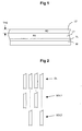
- Figure 1 illustrates a substrate prepared for use with the method, provided with a target layer and two resist layers;
- Figure 2 illustrates the decomposition of a dense line pattern which is beyond lithographic resolution into two semi dense line patterns which each are within lithographic resolution;
- Figure 3 illustrates the first exposure to a first radiation pattern representing semi dense dark lines and bright spaces according to the present invention;
- Figure 4 illustrates the effect of the first exposure and a subsequent development of resist;
- Figure 5 illustrates the second exposure to a radiation pattern representing, in interlaced position with respect to the first radiation pattern, semi dense dark lines and bright spaces according to the present invention;
- Figure 6 shows a resist mask in accordance with a desired dense pattern of lines and spaces according to the invention;
- Figure 7 illustrates a lithographic cluster according to the invention;
- Figure 8 depicts a lithographic apparatus according to an embodiment of the invention, and
- Figure 9 shows a flow scheme of a double exposure method according to the present invention.
- As noted above, their exists a constant need to achieve finer optical resolutions and circumventing the theoretical half-pitch lower limit kl of 0.25 for printing lines using a double exposure process whereby avoiding the use of an intermediate etching step in between the two exposures would provide an important advantage.
- As described in greater detail below, the present invention achieves resolutions lower than the half-pitch lower limit half pitch p 0.5 = k1 • λ/ NA whereby k1 ≥ 0.25, thus circumvention the k1 = 0.25 barrier, by implementing a dual exposure technique whereby use is made of a specially designed sandwich photoresist structure comprising a first resist layer for use to be patterned and to subsequently function as etch mask and a second resist layer which substantially absorbs the exposure radiation and which has a thickness smaller than would be required for functioning as etch mask. Further, the present invention enables the exclusive use of positive tone resist for printing those features whereby the use of positive tone resist is preferable over the use of negative tone resist. Examples of such features are dense, semi dense and isolated lines.
- In the manufacture of integrated circuits (ICs) lithographic exposure apparatuses are used, in which case a patterning device such as a mask (a "reticle") generates a circuit pattern corresponding to an individual layer of the IC. In photolithography, a beam of radiation is, upon traversing the reticle, patterned by a mask pattern embodied, for example, as light-absorbing pattern features (e.g. a chrome layer) on a transparent surface of the reticle. Subsequently, the patterned radiation beam is projected by a projection system of the lithographic apparatus onto a target portion (e.g., comprising one or more dies) on a substrate (such as, for example, a silicon wafer) that has been coated with a layer of photoresist material. An image of the mask pattern is formed by the projection system, and the resist material is exposed to said image. After development of the exposed resist, a desired pattern of resist features is obtained, which in turn can be used as an etch mask for transferring the desired pattern to a target layer underneath the resist layer.
- In general, a single wafer will contain a whole network of adjacent target portions that are successively irradiated via the projection system, one at a time.
- The projected image of the mask pattern provides, at wafer level, a pattern of bright, exposed areas and dark, ideally unexposed but in practice substantially unexposed areas. The resist material layer facing the exposure radiation is exposed to such a radiation pattern, and in the bright areas and due to the exposure to radiation, a photo active compound in the resist is changing the solubility in developer of the resist (generally a resist developer is a basic, aqueous solution). This change of solubility from insoluble to soluble in a positive tone resist (and from soluble to insoluble in a negative tone resist) occurs, over the whole thickness of the resist layer, at a threshold value of the exposure dose, the so called energy-to-clear, hereinafter denoted by Eo.
- In order to decrease the printable half pitch of dense features, the wavelength of the radiation used for exposure is chosen as small as possible (in accordance with Equation 1). Radiation sources generally used for projection lithography are i-line radiation emitting mercury arc lamps, KrF excimer lasers and ArF excimer lasers, providing radiation with a spectral peak at a wavelength of respectively 365 nm, 248 nm and 193 nm.
- Along with the introduction of radiation sources operating at shorter wavelengths, resists had to be developed for each of these radiation wavelengths which are substantially non-absorbing at the wavelength of the radiation to be used for exposure, since any substantial absorption of exposure radiation in a resist material layer would prevent the radiation from activating the photo-active compound of the resist material over the whole thickness of the resist material layer. In conventional lithography, the resist layer thickness shall exceed a minimum thickness needed for a required etch resistance. However, when for example positive tone resist material is used, a too high absorption of exposure radiation could then cause an incomplete developing of an exposed area, leaving residual unexposed resist material in this area after the development of the resist. Hence, the problem of a too high absorbance for a resist layer to be used as etch mask cannot be solved by merely reducing the thickness of the resist material layer. Consequently, for use with lithographic processes based on exposing resist to a pattern image using i-line radiation of a mercury arc lamp, or deep ultra violet (DUV) radiation of respectively an KrF excimer laser and ArF excimer laser, respective substantially non-absorbing resists were developed. For i-line lithography diazonaphthoquinone based resist materials are commonly used. These resists cannot be used with KrF lithography because of strong absorption of radiation of 248 nm wavelength in a layer of diazonaphthoquinone based resist material at sufficient thickness for etch resistance. With the transition to KrF lithography whereby lithography apparatus are used at 248 nm wavelength, chemically amplified resist materials came into use. A chemically amplified resist material features a sufficiently low absorbance for 248 nm radiation. Generally, chemically amplified resists for use with conventional KrF lithography are poly hydroxy styrene based resists. A critical component of chemically amplified resist materials is the photo-acid generator (referred to as PAG), which is the photo-active ingredient. The PAG produces acid upon irradiation. However, in order to achieve sufficient transmittance for radiation of 193 nm wavelength (to enable the use of the chemically amplified resist materials with ArF lithography) new PAGs, such as for example ionic PAG, were introduced and are still in development to further lower the absorbance of a corresponding resist layer at 193 nm radiation-wavelength. Resists for use with conventional ArF lithography are acrylate and/or methacrylate based resists. Hereinafter, a resist type for conventional use with a specific radiation source, and as described above, will be referred to by the specific radiation source: thus, in the present text and claims reference may be made to i-line resist, KrF resist and ArF resist. It is appreciated that each of these resist types has an absorbance beyond tolerance when used (at the required layer thickness for functioning as an etch mask, which may typically be between 200 and 300 nm), with a radiation source operating at a shorter wavelength than said specific radiation source (examples of which are given above).
- According to a first embodiment of the invention, and as illustrated in Figure 1, there is provided a substrate W, which may carry previously processed IC layers, and which is provided, in the following order, with a target layer TL, a first resist
material layer L 1 comprising a first resist material R1, having an energy-to-clear Eo1 and overlaying the target layer TL, and a second resist material layer L2 comprising a second resist material R2 and overlying the first resist layer L1. Providing the resist material layers may include, according to the present invention, applying pre-exposure processes such as for example cleaning, priming and soft-bake processes. To reduce back reflection of exposure radiation during exposure, the second resist material layer L2 may further include a Developable Bottom Anti Reflection Coating to reduce back reflection of exposure radiation, and the first resist material layer L1 may further include a Bottom Anti Reflection Coating or a Developable Bottom Anti Reflection Coating. Both resistlayers L 1 and L2 are to be exposed with radiation of one single type of radiation source. In the present embodiment, the double exposure process is executed using a lithographic exposure apparatus comprising an ArF excimer laser as radiation source, the first resist material R1 is an ArF resist, and the second resist material, a high absorbent material of ArF excimer laser radiation, is a KrF resist. It is appreciated that the invention is not limited to providing and using a stack of ArF and KrF resist layers. For example, the ArF resist layer can be covered by an i-line resist layer (instead of the KrF resist layer); i-line resist is also highly absorbent for ArF excimer laser radiation. - The thickness of the first resist layer L1 is such that, after exposure (to a pattern of radiation as projected on the resist layer L1) and development, it can serve as an etch mask for transfer of the pattern in the developed resist layer to the target layer TL by means of dry etching. According to an aspect of the present invention the thickness TH2 of the second resist material layer L2 is merely chosen such that it is photoactivated throughout its thickness in exposed areas, whilst at the same time preventing exposure of the first resist R1 to an exposure dose greater than the energy-to-clear Eo1 associated with the first resist layer L1. Preferably the thickness TH2 of the second resist material layer L2 is chosen such that it only allows exposure of the first resist R1 to an exposure dose up to only a fraction of the energy-to-clear Eo1. The fraction may preferably be a number smaller than 0.5. Then, after development of the first resist layer, still a sufficient etch resistance is provided for portions of the layer L1 serving as etch mask. It is appreciated that there is no requirement that the resist material layer L2 shall function as an etch-mask.
- The resist material R2 being, in the present embodiment, a KrF resist, strong absorption of ArF excimer laser radiation will occur upon exposure, so that - in the absence of the conventional etch-mask function of patterned resist layers - the thickness TH2 typically can be chosen smaller than the thickness of the resist material layer L1.
- According to an aspect of the invention, and in view of the fact that with the present invention there is no requirement that the patterned resist material layer L2 shall function as an etch-mask, the material of layer L2 can be any suitable positive tone developable material which provides the layer L2 with the desired absorbance.
- As schematically illustrated in Figure 2, the desired pattern to be printed, using a lithographic exposure apparatus, comprises a set DL of dense lines. Conventionally, a mask carrying a corresponding pattern of dense lines is imaged at a 4 or 5 times reduction on the resist layer covering the substrate. According to the present invention, the lines DL are decomposed into two constituent sub-patterns, embodied as corresponding mask patterns SDL1 and SDL2 of semi-dense lines that are capable of being optically resolved by the lithographic apparatus. It is appreciated that on the reticle surface carrying the pattern, the lines may be embodied as, for example, lines of a chrome layer of a Chrome on Glass mask, or of a Mo-Si layer of an attenuated phase shift mask, or as a transparent, 180-degree phase shifting edge of an alternating phase shift mask, or as two or more of such phase shifting edges (separated at a distance smaller than the resolution limit of the lithographic apparatus).
- It is appreciated that the invention is not limited to the use of projection systems operating at 4 or 5 times reduction ratio; for simplicity it is hereinafter assumed that (and the figures are set up as if ) the line printing process is run at unit reduction ratio. According to an aspect of the invention, lines of resist layer material in accordance with the
sub patterns SDL 1 and SDL2 are provided to the target layer TL (and hence protruding from the target layer surface) by subsequently imaging the patterns in interlaced position relative to each other, on the wafer surface, as described in more detail below. - After providing the substrate to a lithographic projection apparatus, the substrate is subjected to a first exposure process whereby the second resist material layer L2 is exposed to an
image 310 of the sub-pattern SDL1, as illustrated in Figure 3. - The
image 310 comprises bright areas ofexposure 300, whereby the length of thearrows 301 schematically indicates the magnitude of the exposure dose Ein applied to the second resist material layer L2 in these areas. Theimage intensity pattern 310 further comprisesdark areas 302 corresponding to lines of the first sub-pattern SDL1, where the layer L2 remains unexposed. Due to absorption of exposure radiation in the second resist material layer L2, exposure of the first resist R1 is substantially avoided; in particular exposure to an exposure dose greater than the energy-to-clear Eo1 is avoided. The resist layer L1 underneath the areas ofexposure 300 will in principle be exposed to an exposure dose which is leaking through the absorbing second resist material layer L2 during exposure. This exposure dose is referred to as the leakage dose, and is denoted by Eout. The leakage of exposure dose is schematically indicated by thearrows 303 in Figure 3; the length of thearrows 303 schematically indicates the magnitude of the leakage dose Eout. The leakage dose Eout leaking through layer L2 is related to the exposure dose Ein of the first exposure according to:
where A is the absorbance of the second layer L2. To avoid exposure to an exposure dose greater than the energy-to-clear Eo1 the thickness of the second layer is chosen such that A > Ao, where Ao is the absorbance of the layer L2 at which Eout = Eo1, thus where the equation
- Preferably (to maintain sufficient thickness of the first resist material layer after developing that layer in a subsequent process step described below) the leakage dose Eout is arranged to be a fraction x of the energy to clear Eo1 by choosing the thickness TH2 of the second layer such that A > Ax, where Ax is the absorbance of the layer L2 at which Eout = x ·Eo1, with x < 0.5:

- The absorbance A of the second resist layer L2 is to good approximation linearly proportional to the thickness TH2. For example, the absorbance may be modelled as follows:

where ε is the molar absorptivity of the PAG, and c the concentration of the PAG. - Further, the thickness TH2 of the second resist material layer L2 is chosen such that it is photoactivated throughout its thickness in exposed areas.
- In the present embodiment, after the first exposure, the exposed resist material R2 is removed by a first resist development process. As schematically illustrated in Figure 4, unexposed resist material R2 remains and hence a mask of line shaped
features 400 of resist material R2 corresponding to the lines of the first sub pattern SDL1 is obtained on the resist material layer L1. The line shape features are protruding from the resist material layer L1.
After applying the first exposure and before applying the first resist development process, the substrate may or may not (depending on the material properties of the resist material R2) be subjected to post-exposure processes such as for example a Post Exposure Bake (PEB) and a hard bake. If the substrate is subjected to, for example, a Post Exposure Bake (PEB) and/or a hard bake, an effect of these steps on the resist material R1 may be compensated by adjusting the exposure dose of a second exposure (described below). The spaces between the semidense lines 400 of unexposed resist material R2 defineareas 401 in the resist material layer L1 where the resist material R1 has been exposed to the leakage dose Eout (an exposure dose preferably well below energy-to-clear Eo1). The below energy-to-clear exposure of theareas 401 is indicated in Figure 4 by the grey filling of theareas 401. Thus, after the first exposure, the resist material R1 has either been exposed below Energy-to-clear Eo1, or it has not been exposed (in accordance with the dark areas of theimage 310, and ignoring any insubstantial exposure such as exposure to stray radiation). - According to the present embodiment, and as illustrated in Figure 5, the first resist material layer L1 and the line shaped
features 400 of unexposed resist material R2 are exposed, during a second exposure process, to apattern 510 of ArF excimer laser exposure radiation in accordance with the second sub pattern SDL2, comprising dark semidense lines 502 embedded in bright background areas ofexposure 500. Thepattern 510 is an image of the mask line pattern SDL2, also referred to hereinafter as the second image, and is located with respect to thelines 400 such that the bright areas of theimage 510 are positioned in interlaced position with respect to thelines 400. So, the lines of the pattern SDL2 are positioned in between the previously obtained line features 400. In the areas corresponding to thebright spaces 500 between thedark lines 502 of thesecond image 510 the absorbance of the KrF resist features 400 prevents exposure of resist material R1 underneath these features to a dose above energy-to-clear Eol. Where, in view of the previous exposure, the thickness TH2 of the second resist material layer L2 was chosen (as described above) such that it allows exposure of the first resist R1 to an exposure dose up to only a fraction 0.5 or less of the energy-to-clear Eol, the absorbance of the KrF resist features 400 in this exposure as well prevents a too high exposure of resist material R1 underneath these features in the same way and substantially under the same physical circumstances. - The process of exposure dose leaking through the KrF resist material features 400 is the same as the exposure dose leakage process during the first exposure, i.e., it is governed by substantially the same physical conditions such as Equations 1-5. This is schematically indicated by the larger and smaller vertical arrows in Figure 5, corresponding to the
respective arrows features 400 is substantially the same as the below energy-to-clear exposure to radiation that had occurred before start of the second exposure in thedark areas 502. In analogy with theareas 401, this is indicated by the grey filled areas 401' (corresponding to the dark lines 502) and 504 (underneath the features 400) in Figure 5. The resist layer material R1 is fully exposed to an exposure dose Ein in theareas 505 between theareas 401' and 504. - In the present embodiment, after the second exposure, the resist material features 400 and the exposed resist material R1 in the
areas 505 are removed by applying a second resist development process. Unexposed resist material R1 and/or resist material R1 exposed below energy-to-clear Eo, as described above, remains and hence, on the target layer TL an etch-mask of line shaped features of resist material R1, corresponding to the lines of the desired pattern DL and protruding from thesurface 600 of the target layer, is obtained as indicated in Figure 6. After the second exposure, the substrate may again be subjected to post-exposure processes such as for example a Post Exposure Bake (PEB) and a hard bake. - The pattern of resist material features can be used as etch-mask for the transfer of the desired pattern DL to the target layer using for example conventional reactive ion etching. Such a final transfer of the pattern to the target layer TL may, for example, involve an etching using a dry etching chamber, suitable for reactive ion etching. An advantage of Reactive Ion Etching, also referred to as RIE, is that it is a non-isotropic, directionally selective etch process, whereas wet etching is an isotropic etch process (causing undercut of features).
- As further illustrated in Figure 6 by the similar grey filling of the
areas 401' and 504, the exposure to radiation (below energy-to-clear) of the resistfeatures 600 is the same for the lines of the two sub patterns, provided that the exposure dose Ein for the first and second exposure process is substantially the same. Hence, to the extent that exposure to such a below energy to clear exposure dose has an effect on, for example, etch resistance, or an etching-bias, this effect is uniformly distributed over the lines of the mask pattern, thereby providing process uniformity. - According to an aspect of the invention, the leakage dose Eout is a fraction x of the energy to clear Eo1 in which case the leakage dose Eout equals , in the first and second exposure of the present embodiment, a threshold dose whereby only a layer-shaped portion of the resist material of the layer L1, the layer-shaped portion facing the exposure radiation, becomes soluble. Consequently, during the two exposures that layer-shaped portion (or "upper section") of the first resist
material layer L 1 is exposed above development threshold and will be developed away during the application of the respective first and second development processes. Due to residual absorption of exposure radiation in the ArF resist layer L1, the effect of exposure to above the threshold dose remains limited to said layer-shaped upper section, so that the absorbance A still prevents exposure to above said threshold dose of at least a portion of the first resist material R1 underneath exposed areas during exposing the second layer L2 and underneath saidfeatures 400 during exposing the first layer and said features 400. Since again both the exposure in said layer shaped upper section and in the portion of the resistmaterial layer L 1 underneath the upper section are governed by substantially the same physical conditions during the two exposures, any effect on etch resistance, or on an etching-bias, is uniformly distributed over the lines of the mask pattern, thereby maintaining above mentioned process uniformity. - An aspect of the invention is that the method is suitable for printing dense and semi dense lines (or substantially line-shaped features or elongated features, preferably at critical dimension) because the method involves the use of positive tone resist for the first and second exposure. An imaging process for printing lines is of optimal quality when imaging dark lines against a bright background. With the present invention this optimal quality can be obtained by using positive resist with the lithographic processes for printing the line features of the resist masks formed in the resist material layers L2 and L1.
- The lithographic exposure apparatus used for printing the lines generally comprises a support structure constructed to support a patterning device (e.g., a mask), and a substrate table (e.g., a wafer table) constructed to hold the substrate W. The lithographic exposure apparatus may be of a type having two (dual stage) or more substrate tables (and/or two or more mask tables). In such "multiple stage" machines the additional tables may be used in parallel, or preparatory steps may be carried out on one or more tables while one or more other tables are being used for exposure. Residual placement errors during e-beam writing of the masks for the patterns SDL1 and SDL2 can be monitored and in a dual stage lithographic projection system these residual errors can be compensated for when the dual stage apparatus is used in a mode of operation whereby he scanner "remembers" the wafer chuck used for the 1st exposure and dedicates the same wafer chuck for the second exposure. This mode of operation will be referred to hereinafter as the chuck-dedication-mode. As a result, in the chuck-dedication-mode, the wafer stepping grid and the wafer table chucking induced distortions fingerprints will be the same for the first and second exposures. This reduces non-correctable higher order overlay errors between these two exposures. In addition, the low order e-beam mask writer's pattern placement errors, e.g., linear offsets and magnification errors, between two masks can be compensated in the scanner by using the appropriate alignment compensations for the wafer stage and the reticle stage. In the chuck-dedication-mode the overlay performance with the present double exposure process is comparable to, or even better than the mask-writer's placement accuracy.
- An aspect of the present invention is that lines are printed, instead of spaces. Alignment errors between the two exposures do not affect the resulting printed line width, but only the spaces between the lines, which is generally less critical to, for example, transistor performance. A placement error between the
sub-patterns SDL 1 and SDL2, i.e., the overlay consistency between the two exposures of the double exposure process, has no effect on the printed critical dimension of the resulting lines. This placement error can be of the order of the placement error as occurring during the mask writing process. By using positive resist with the lithographic processes for printing the lines of the patterns SDL1 and SDL2 any overlay error of the patterns SDL1 and SDL2, and hence also of the resulting pattern DL, with respect to a pattern which was previously formed on the substrate W is the same as would have been obtained with a single exposure process. In other words, the resulting alignment accuracy of the pattern DL in the target layer TL with respect to a reference on the substrate W directly corresponds to the alignment accuracy obtainable with a single-exposure process. - Due to any non-linearity of the response of a photoresist layer to either development and/or exposure, the spatial Fourier transformation of the resist-mask of
features 400 corresponding to the sub-pattern SDL1, contain higher spatial frequencies than the spatial Fourier transformation of the intensity pattern of the image of the sub-pattern SDL1. The first exposure and development of the resist R2 fixes the first sub-pattern image in the second resist material layer L2, and thefeatures 400 of resist material R2 act as a contact mask during the second exposure, thus preventing a cross talk or a merging of the two sub-pattern images corresponding to thepatterns SDL 1 and SDL2. Therefore, also the spatial Fourier transformation of the combined pattern DL as transferred to the target layer (using thefeatures 600 as etch-mask) contains spatial frequencies higher than corresponding to the inverse of a half pitch p 0.5 = k1 • λ/NA whereby k1 ≥ 0.25, which enables the circumvention of the k1 = 0.25 barrier. - According to an aspect of the invention the target layer TL may either be an IC-layer (such as for example a doped polysilicon layer) or a hard mask layer which is to act as an etch-mask.
- According to the present invention neither a deposition of a hard mask layer nor an etching of a hard mask layer between the two exposures is needed. Instead, the present exposure and line printing method in principle only uses a conventional aqueous development steps, one between the two exposures, and one after the second exposure. Consequently, the present method can easily be implemented in a lithographic system comprising the lithographic apparatus and a coat/develop track that is typically linked to the lithographic apparatus.
- A lithographic system suitable for use with conventional double exposure processes generally comprises a plurality of resist development devices and substrate coating devices, such as a spin-coat device for applying a resist layer onto the substrate. According to an aspect of the present invention, and as illustrated in Figure 7, a
lithographic system 70 comprises, besides alithographic exposure apparatus 71, a spin-coat device 72 capable of providing to the substrate the resist material layer L2, and acontrol device 73 for controlling the lithographic exposure apparatus and the spin-coat device. The spin-coat device may be arranged to provide a resist layer of a preselected thickness to the substrate, whereby this process is fully automated and run under computer control. The thickness of the resist layer as applied by the spin-coat device is controlled by a number of parameters comprising for example, the rotation speed used for spin-coating, the temperature of the resist material, the amount of resist material applied to the substrate W during spin-coating, and the viscosity of the resist material. - One or more spin-coat devices may be used to respectively apply the first and second resist material layers L1 and L2.
- A lithographic exposure apparatus according to an embodiment of the invention is schematically depicted in Figure 8. The apparatus comprises:
- an illumination system (illuminator) IL configured to condition a radiation beam B (e.g., UV radiation or DUV radiation such as for example generated by an excimer laser operating at a wavelength of 193 nm or 157 nm, or EUV radiation generated by a laser-fired plasma source operating at 13,6 nm).
- a support structure (e.g., a mask table) MT constructed to support a patterning device (e.g., a mask) MA and connected to a first positioner PM configured to accurately position the patterning device in accordance with certain parameters;
- a substrate table (e.g., a wafer table) WT constructed to hold a substrate (e.g., a resist-coated wafer) W and connected to a second positioner PW configured to accurately position the substrate in accordance with certain parameters; and
- a projection system (e.g., a refractive projection lens system) PS configured to project a pattern imparted to the radiation beam B by patterning device MA onto a target portion C (e.g., comprising one or more dies) of the substrate W.
- The illumination system may include various types of optical components, such as refractive, reflective, magnetic, electromagnetic, electrostatic or other types of optical components, or any combination thereof, for directing, shaping, or controlling radiation.
- The support structure may be a frame or a table, for example, which may be fixed or movable as required. The support structure may ensure that the patterning device is at a desired position, for example with respect to the projection system. Any use of the terms "reticle" or "mask" herein may be considered synonymous with the more general term "patterning device."
- The term "patterning device" used herein should be broadly interpreted as referring to any device that can be used to impart a radiation beam with a pattern in its cross-section such as to create a pattern in a target portion of the substrate. It should be noted that the pattern imparted to the radiation beam may not exactly correspond to the desired pattern in the target portion of the substrate, for example if the pattern includes phase-shifting features or so called assist features. Generally, the pattern imparted to the radiation beam will correspond to a particular functional layer in a device being created in the target portion, such as an integrated circuit. The patterning device may be transmissive or reflective.
- The term "projection system" used herein should be broadly interpreted as encompassing any type of projection system, including refractive, reflective, and catadioptric optical systems, or any combination thereof, as appropriate for the exposure radiation being used, or for other factors such as the use of an immersion liquid or the use of a vacuum. Any use of the term "projection lens" herein may be considered as synonymous with the more general term "projection system".
- As here depicted, the apparatus is of a transmissive type (e.g., employing a transmissive mask). Alternatively, the apparatus may be of a reflective type (e.g., employing a reflective mask).
- The lithographic apparatus may be of a type having two (dual stage) or more substrate tables (and/or two or more mask tables). In such "multiple stage" machines the additional tables may be used in parallel, or preparatory steps may be carried out on one or more tables while one or more other tables are being used for exposure.
- The lithographic apparatus may also be of a type wherein at least a portion of the substrate may be covered by a liquid having a relatively high refractive index, e.g., water, so as to fill a space between the projection system and the substrate. An immersion liquid may also be applied to other spaces in the lithographic apparatus, for example, between the mask and the projection system. Immersion techniques are well known in the art for increasing the numerical aperture of projection systems. The term "immersion" as used herein does not mean that a structure, such as a substrate, must be submerged in liquid, but rather only means that liquid is located between the projection system and the substrate during exposure.
- Referring to Figure 8, the illuminator IL receives a radiation beam from a radiation source SO. The source and the lithographic apparatus may be separate entities, for example when the source is an excimer laser. In such cases, the source is not considered to form part of the lithographic apparatus and the radiation beam is passed from the source SO to the illuminator IL with the aid of a beam delivery system BD comprising, for example, suitable directing mirrors and/or a beam expander. In other cases the source may be an integral part of the lithographic apparatus, for example when the source is a mercury lamp. The source SO and the illuminator IL, together with the beam delivery system BD if required, may be referred to as a radiation system.
- The illuminator IL may comprise an adjuster AD for adjusting the angular intensity distribution of the radiation beam. Generally, at least the outer and/or inner radial extent (commonly referred to as σ-outer and σ-inner, respectively) of the intensity distribution in a pupil plane of the illuminator can be adjusted. In addition, the illuminator IL may comprise various other components, such as an integrator IN and a condenser CO. The illuminator may be used to condition the radiation beam, to have a desired uniformity and intensity distribution in its cross-section.
- The radiation beam B is incident on the patterning device (e.g., mask MA), which is held on the support structure (e.g., mask table MT), and is patterned by the patterning device. Having traversed the mask MA, the radiation beam B passes through the projection system PS, which focuses the beam onto a target portion C of the substrate W. With the aid of the second positioner PW and position sensor IF (e.g., an interferometric device, linear encoder or capacitive sensor), the substrate table WT can be moved accurately, e.g., so as to position different target portions C in the path of the radiation beam B. Similarly, the first positioner PM and another position sensor (which is not explicitly depicted in Figure 8) can be used to accurately position the mask MA with respect to the path of the radiation beam B, e.g., after mechanical retrieval from a mask library, or during a scan. In general, movement of the mask table MT may be realized with the aid of a long-stroke module (coarse positioning) and a short-stroke module (fine positioning), which form part of the first positioner PM. Similarly, movement of the substrate table WT may be realized using a long-stroke module and a short-stroke module, which form part of the second positioner PW. In the case of a stepper (as opposed to a scanner) the mask table MT may be connected to a short-stroke actuator only, or may be fixed. Mask MA and substrate W may be aligned using mask alignment marks M1, M2 and substrate alignment marks P1, P2. Although the substrate alignment marks as illustrated occupy dedicated target portions, they may be located in spaces between target portions (these are known as scribe-lane alignment marks). Similarly, in situations in which more than one die is provided on the mask MA, the mask alignment marks may be located between the dies.
- The depicted apparatus could be used in at least one of the following modes:
- 1. In step mode, the mask table MT and the substrate table WT are kept essentially stationary, while an entire pattern imparted to the radiation beam is projected onto a target portion C at one time (i.e., a single static exposure). The substrate table WT is then shifted in the X and/or Y direction so that a different target portion C can be exposed. In step mode, the maximum size of the exposure field limits the size of the target portion C imaged in a single static exposure.
- 2. In scan mode, the mask table MT and the substrate table WT are scanned synchronously while a pattern imparted to the radiation beam is projected onto a target portion C (i.e., a single dynamic exposure). The velocity and direction of the substrate table WT relative to the mask table MT may be determined by the (de-)magnification and image reversal characteristics of the projection system PS. In scan mode, the maximum size of the exposure field limits the width (in the non-scanning direction) of the target portion in a single dynamic exposure, whereas the length of the scanning motion determines the height (in the scanning direction) of the target portion.
- 3. In another mode, the mask table MT is kept essentially stationary holding a programmable patterning device, and the substrate table WT is moved or scanned while a pattern imparted to the radiation beam is projected onto a target portion C. In this mode, generally a pulsed radiation source is employed and the programmable patterning device is updated as required after each movement of the substrate table WT or in between successive radiation pulses during a scan. This mode of operation can be readily applied to maskless lithography that utilizes programmable patterning device, such as a programmable mirror array of a type as referred to above.
- Combinations and/or variations on the above described modes of use or entirely different modes of use may also be employed.
- According to an aspect of the invention the lithographic system comprises, as lithographic exposure apparatus, a lithographic interferometry apparatus. In such an apparatus, a resist layer is exposed to a fringe pattern obtained in a multiple beam interferometric apparatus. For example, two collimated beams of UV or DUV radiation intersect each other at an angle to produce linear interference fringes. A wafer having a photosensitive layer is positioned on a movable table. The table is arranged to be rotated and translated in two-dimensions respectively. Two substantially collimated coherent optical beams provided by any suitable well known source or sources are directed at a variable angle from the normal vector associated with the wafer toward each other and toward the photoresist layer to form an interference pattern on the photosensitive layer. The interfering radiation beams of coherent radiation may be generated by, for example, an ArF excimer laser using a beam splitting element, and may be provided in any suitable well known manner so that they are from the same source and are essentially equal in intensity at the wafer which assures a high contrast exposure.
- The interference pattern produced on the photoresist layer or layers may be varied by for example rotating the wafer and/or translating the wafer.
- The
control device 73, see Figure 7, according to the present invention may comprise a memory into which data can be stored which concern thesub-patterns SDL 1 and SDL2 and which are used for controlling the lithographic exposure apparatus 71 (such as, for example, settings concerning positioning of the stages MT and WT, and/or settings concerning illumination modes) during each of the two exposures required to generate the combined pattern DL. The same memory can be used to store data concerning the settings of the spin-coat device 72 used for providing the second resist material layer L2 to the substrate W in accordance with the present invention. A computer which may be part of the control device is programmed and arranged to execute, based on the data stored in the memory, any of the method steps according to the present invention. - Figure 9 illustrates the method steps 900 according to the invention. The execution of the steps involves running a computer program on said computer, said computer program containing one or more sequences of machine-readable instructions describing any of the methods as disclosed above. The computer contains a machine readable medium (e.g., semiconductor memory, magnetic or optical disk) having such a computer program stored therein.
- According to an aspect of the invention the machine readable medium is encoded with machine executable instructions for patterning a substrate according to the
steps 900. A substrate W provided with a target layer TL and the first resist material layer L1 is provided (step 902) to the spin-coat device, which may involve a substrate handler transporting the substrate from thelithographic exposure apparatus 71 to the spin-coat device 72. Next, instep 906, the required thickness TH2 of the second resist layer L2 such that the absorbance A prevents exposure to above energy-to-clear exposure dose Eo of at least a portion of the first resist R1 underneath exposedareas 301 during exposing the second layer L2 (and underneath thefeatures 400 during exposing the first layer L1 carrying said features 400) is determined. - To that purpose,
data 904 comprising data concerning the resist materials R1 and R2, data concerning the respective absorbencies such as for example parameters ε (the molar absorptivity of the PAG) and c (the concentration of the PAG), and data concerning the first and second exposure are obtained. The latter data may involve the properties of the patterns SDL1 and SDL2, such as for example the type of mask and a critical dimension bias, as well as exposure doses to be applied. - The determination of the thickness TH2 in
step 906 may for example involves calculating absorbencies and applying equations 1-4. The determination may include calculating a minimum thickness value for TH2, based on, for example, a predetermined absorptivity of the second resist material, whereby exposure of the first resist R1 to an exposure dose up to only a fraction of the energy-to-clear Eo1 is safeguarded. The fraction may preferably be a number smaller than 0.5. - The determination may further include calculating a maximum thickness value for TH2, based on, for example, a predetermined absorptivity of the second resist material, whereby the requirement that the second resist material layer L2 is photoactivated throughout its thickness in exposed areas is fulfilled. Alternatively, look-up tables of absorbance values may be used. In
step 908 the settings for the spin-coater are determined, based on the results of thedetermination step 906, and instep 910 these settings are applied to the spin-coater, so that the resistmaterial layer L 1 can be properly covered with the resist material layer L2 in accordance with the present invention. - Next, the substrate is transported to the lithographic apparatus 71 (step 912) which again may involve the use of substrate handler and transporting devices. In the
steps 914 the first exposure is executed in accordance with the present embodiment, and the first resist development process is applied instep 916. Similarly, in thesteps data 904 may further comprise sub-pattern overlay data and positioning data for reticles with the patterns SDL1 and SDL2 respectively. Therefore, these data shall be obtained and used in thesteps step 920, this resistpattern 600 is obtained. - A second embodiment of the invention is the same as the first embodiment of the invention described above, safe for the choice of resist material R2. In this embodiment, the resist material R2 is i-line resist, which just as KrF resist absorbs radiation of 193 nm wavelength. Alternatively, the resist material L2 comprises a positive tone resist different from i-line resist or KrF resist and with sufficient absorption for 193 nm radiation to provide an absorbance to the layer L2 in accordance with the present invention, and as described in the first embodiment.
- A third embodiment of the invention is the same as the first embodiment of the invention described above, safe for the radiation source and for the choice of the resist materials R2 and R1 as combination. In this embodiment, the first resist material R1 is KrF resist, and the source SO a KrF excimer laser. The resist material R2 may for example be an i-line resist. Alternatively, the resist material L2 comprises a positive tone resist different from i-line resist and with sufficient absorption for 248 nm radiation to provide an absorbance to the layer L2 in accordance with the present invention, in analogy to the first embodiment.
- Similarly, in a fourth embodiment of the invention the radiation source SO is an i-line mercury arc and the first resist material R1 is an i-line resist. The resist material R2 in the present embodiment is a positive tone resist with sufficient absorption for i-line radiation to provide an absorbance to the layer L2 in accordance with the present invention, in analogy to the first embodiment.
- Although specific reference may be made in this text to the use of lithographic apparatus in the manufacture of ICs, it should be understood that the lithographic apparatus described herein may have other applications, such as the manufacture of integrated optical systems, guidance and detection patterns for magnetic domain memories, flat-panel displays, liquid-crystal displays (LCDs), thin-film magnetic heads, etc. The skilled artisan will appreciate that, in the context of such alternative applications, any use of the terms "wafer" or "die" herein may be considered as synonymous with the more general terms "substrate" or "target portion," respectively. The substrate referred to herein may be processed, before or after exposure, in for example a track (a tool that typically applies a layer of resist to a substrate and develops the exposed resist), a metrology tool and/or an inspection tool. Where applicable, the disclosure herein may be applied to such and other substrate processing tools. Further, the substrate may be processed more than once, for example in order to create a multi-layer IC, so that the term substrate used herein may also refer to a substrate that already contains multiple processed layers.
- The terms "radiation" and "beam" used herein encompass all types of electromagnetic radiation, including ultraviolet (UV) radiation (e.g., having a wavelength of or about 365, 355, 248, 193, 157 or 126 nm) and extreme ultra-violet (EUV) radiation (e.g., having a wavelength in the range of 5-20 nm), as well as particle beams, such as ion beams or electron beams.
- The term "lens", where the context allows, may refer to any one or combination of various types of optical components, including refractive, reflective, magnetic, electromagnetic and electrostatic optical components.
- While specific embodiments of the invention have been described above, it will be appreciated that the invention may be practiced otherwise than as described.
- The descriptions above are intended to be illustrative, not limiting. Thus, it will be apparent to one skilled in the art that modifications may be made to the invention as described without departing from the scope of the claims set out below.
Claims (18)
- A substrate constructed and arranged for being patterned using a lithographic process
wherein the substrate is exposed to radiation, comprising:a first layer of a first positive tone developable material at least partially overlying the substrate; anda second layer, of a second positive tone developable material, with a preselected absorbance for the radiation and at least partially overlying the first layer,wherein the absorbance is arranged to, during exposure to radiation of the second layer,prevent exposure of at least a portion of the first positive tone developable material underneath the second positive tone developable material to an exposure dose exceeding a fraction of an energy-to-clear exposure dose associated with the first layer, andprovide substantially complete photoactivation of the second layer. - A substrate according to claim 1 wherein the second positive tone developable material is a positive tone resist material.
- A substrate according to claim 1 or 2 wherein the first positive tone developable material is an ArF resist or an acrylate/methacrylate based resist.
- A substrate according to claim 1 or 2 wherein the first positive tone developable material is an ArF resist or an acrylate/methacrylate based resist, and wherein the second positive tone developable material is a KrF resist or a poly hydroxy styrene based resist.
- A substrate according to claim 1 or 2 wherein the first positive tone developable material is a KrF resist or a poly hydroxy styrene based resist, and wherein the second positive tone developable material an i-line resist or a diazonaphthoquinone based resist.
- A substrate according to any one of claims 1 to 5 wherein the fraction of the energy-to-clear exposure dose associated with the first layer is smaller than 0.5.
- A method of forming a pattern of dense features of resist material on a substrate, including exposing the substrate to radiation traversing a patterning device, said substrate including
a first layer of a first positive tone developable material at least partially overlying the substrate,
the method comprising:providing to the first layer a second layer of a second positive tone developable material with an absorbance higher than an absorbance of the first layer;identifying in the pattern two interlaced patterns of semi-dense features;splitting the pattern in a corresponding first and second pattern with associated respective first and second radiation patterns wherein the semi-dense features correspond to dark features in a bright background;exposing the second layer to the first radiation pattern;developing the second positive tone developable material, to provide a pattern of features protruding from the first layer, separated by areas of uncovered first resist material;exposing the uncovered first layer and the protruding features to the second radiation pattern whereby the dark features are positioned in interlaced relation with respect to the protruding features, anddeveloping the first developable material to provide the pattern of dense features. - A method according to claim 7 wherein the absorbance of the second layer is arranged to prevent, during exposing, an exposure of at least a portion of the first positive tone developable material underneath the second positive tone developable material to an exposure dose exceeding a fraction of an energy-to-clear exposure dose associated with the first layer, and to provide substantially complete photoactivation of the second layer.
- A method according to claim 8 wherein the fraction of the energy-to-clear exposure dose associated with the first layer is smaller than 0.5.
- A method according to any one of claims 7 to 9 wherein the second positive tone developable material is a second positive tone resist different from the first positive tone developable material.
- A method according to any one of claims 7 to 9 wherein the radiation is ArF excimer laser radiation and the first developable material is an ArF resist or a acrylate/methacrylate based resist.
- A method according to claim 10 wherein the radiation is ArF excimer laser radiation and the first developable material is an ArF resist or an acrylate/methacrylate based resist and
wherein the second developable material is an i-line resist or a diazonaphthoquinone based resist or a KrF resist or a poly hydroxy styrene based resist. - A method according to claim 10 wherein the radiation is KrF excimer laser radiation and the first developable material is a KrF resist material or a poly hydroxy styrene based resist and wherein the second developable material is an i-line resist or a diazonaphthoquinone based resist.
- A method according to any one of claims 7 to 13 wherein the dense features are dense line-shaped features.
- A computer program comprising machine executable instructions for instructing a lithographic system to pattern a substrate according to an exposure method using patterned radiation and comprising:providing to a spin-coat device a substrate having a target layer arranged to be lithographically patterned with a desired pattern comprising a first sub pattern and a second sub pattern, and having a first layer of a first positive tone developable material at least partially overlying the target layer;obtaining data for determining an absorbance of a second layer of a second positive tone developable material to be disposed on the first layer;determining a thickness of the second layer based on said data and in accordance with the absorbance preventing exposure of at least a portion of the first layer underneath exposed portions of the second positive tone developable material during an exposure of the second developable material to the radiation;determining settings for the spin-coat device based on the determined thickness, applying the settings and providing the second layer to the first layer;exposing the substrate to a first pattern of the radiation in accordance with the first sub pattern;developing the second positive tone developable material;exposing the substrate to a second pattern of the radiation in accordance with the second sub pattern; anddeveloping the first positive tone developable material.
- A computer program according to claim 15 whereby the second positive tone developable material is a second positive tone resist different from the positive tone developable material of the first layer.
- A lithographic system comprising a lithographic exposure apparatus, a spin-coat device capable of providing a layer of developable material to a substrate, and a control device for controlling the lithographic exposure apparatus and spin-coat device, whereby the control device effects the program according to claim 15 or 16.
- A system according to claim 17 wherein the lithographic exposure apparatus is one of a lithographic projection apparatus and a lithographic interferometry apparatus.
Applications Claiming Priority (1)
| Application Number | Priority Date | Filing Date | Title |
|---|---|---|---|
| US11/234,399 US7582413B2 (en) | 2005-09-26 | 2005-09-26 | Substrate, method of exposing a substrate, machine readable medium |
Publications (2)
| Publication Number | Publication Date |
|---|---|
| EP1906257A2 true EP1906257A2 (en) | 2008-04-02 |
| EP1906257A3 EP1906257A3 (en) | 2008-08-20 |
Family
ID=37894470
Family Applications (1)
| Application Number | Title | Priority Date | Filing Date |
|---|---|---|---|
| EP06254878A Withdrawn EP1906257A3 (en) | 2005-09-26 | 2006-09-20 | Substrate, method of exposing a subsrate, machine readable medium |
Country Status (7)
| Country | Link |
|---|---|
| US (2) | US7582413B2 (en) |
| EP (1) | EP1906257A3 (en) |
| JP (1) | JP4036884B2 (en) |
| KR (1) | KR100846185B1 (en) |
| CN (1) | CN1952790B (en) |
| SG (1) | SG131074A1 (en) |
| TW (1) | TWI329889B (en) |
Families Citing this family (19)
| Publication number | Priority date | Publication date | Assignee | Title |
|---|---|---|---|---|
| TW200707114A (en) * | 2005-08-12 | 2007-02-16 | Chi Lin Technology Co Ltd | Method for forming an interference fringe and method for forming an interference pattern |
| US7582413B2 (en) * | 2005-09-26 | 2009-09-01 | Asml Netherlands B.V. | Substrate, method of exposing a substrate, machine readable medium |
| JP5032948B2 (en) | 2006-11-14 | 2012-09-26 | エーエスエムエル マスクツールズ ビー.ブイ. | Method, program and apparatus for performing pattern decomposition used in the DPT process |
| TWI334163B (en) * | 2007-03-30 | 2010-12-01 | Nanya Technology Corp | Method of pattern transfer |
| NL1035771A1 (en) * | 2007-08-20 | 2009-02-23 | Asml Netherlands Bv | Lithographic Method and Method for Testing a Lithographic Apparatus. |
| JP2009164441A (en) * | 2008-01-09 | 2009-07-23 | Panasonic Corp | Pattern formation method |
| US8043794B2 (en) * | 2008-02-01 | 2011-10-25 | Qimonda Ag | Method of double patterning, method of processing a plurality of semiconductor wafers and semiconductor device |
| NL2004531A (en) * | 2009-05-29 | 2010-11-30 | Asml Netherlands Bv | APPARATUS AND METHOD FOR PROVIDING RESIST ALIGNMENT MARKS IN A DOUBLE PATTERNING LITHOGRAPHIC PROCESS. |
| JP5479070B2 (en) | 2009-12-17 | 2014-04-23 | 株式会社東芝 | Optical image intensity calculation method, pattern generation method, semiconductor device manufacturing method, and optical image intensity distribution calculation program |
| US8423923B2 (en) * | 2011-07-20 | 2013-04-16 | United Microelectronics Corp. | Optical proximity correction method |
| US8883403B2 (en) * | 2012-09-14 | 2014-11-11 | Taiwan Semiconductor Manufacturing Company, Ltd. | Method of semiconductor integrated circuit fabrication |
| EP3472672A4 (en) * | 2016-06-20 | 2020-03-04 | Nikon Corporation | DENSITY LINE EXTREME ULTRAVIOLET LITHOGRAPHY SYSTEM WITH DISTORTION ADAPTATION |
| CN106842825B (en) * | 2017-03-21 | 2021-01-12 | 京东方科技集团股份有限公司 | Master mold and method for manufacturing same |
| JP6942555B2 (en) * | 2017-08-03 | 2021-09-29 | 東京エレクトロン株式会社 | Board processing method, computer storage medium and board processing system |
| US11289376B2 (en) * | 2019-07-31 | 2022-03-29 | Taiwan Semiconductor Manufacturing Co., Ltd | Methods for forming self-aligned interconnect structures |
| US11796922B2 (en) * | 2019-09-30 | 2023-10-24 | Taiwan Semiconductor Manufacturing Co., Ltd. | Method of manufacturing semiconductor devices |
| TWI833601B (en) * | 2022-07-01 | 2024-02-21 | 南亞科技股份有限公司 | Method of processing a substrate |
| US12436465B2 (en) | 2022-07-01 | 2025-10-07 | Nanya Technology Corporation | Method of processing a substrate |
| TWI907962B (en) * | 2024-02-20 | 2025-12-11 | 華邦電子股份有限公司 | Photo-mask pattern |
Family Cites Families (23)
| Publication number | Priority date | Publication date | Assignee | Title |
|---|---|---|---|---|
| JPH01191130A (en) | 1988-01-26 | 1989-08-01 | Fujitsu Ltd | Minute pattern forming method |
| JPH0279045A (en) | 1988-09-14 | 1990-03-19 | Fujitsu Ltd | Resist pattern forming method |
| JPH05275316A (en) | 1992-03-30 | 1993-10-22 | Oki Electric Ind Co Ltd | Formation of resist pattern |
| US6042998A (en) * | 1993-09-30 | 2000-03-28 | The University Of New Mexico | Method and apparatus for extending spatial frequencies in photolithography images |
| DE4440230C2 (en) * | 1993-11-10 | 1999-03-18 | Hyundai Electronics Ind | Process for forming fine structures of a semiconductor device |
| JP2000194141A (en) | 1998-12-28 | 2000-07-14 | Kansai Paint Co Ltd | Method of forming resist pattern |
| US6107006A (en) * | 1999-01-18 | 2000-08-22 | Winbond Electronics Corp. | Method for forming pattern |
| JP2001033984A (en) | 1999-07-15 | 2001-02-09 | Mitsubishi Electric Corp | Pattern forming method, semiconductor device manufacturing method using the same, and semiconductor device |
| EP1077468A1 (en) * | 1999-08-16 | 2001-02-21 | Matsushita Electronics (Europe) GmbH | Colour cathode ray tube with tension mask |
| JP4613364B2 (en) | 2000-06-14 | 2011-01-19 | 学校法人東京電機大学 | Resist pattern formation method |
| US6589713B1 (en) * | 2001-01-29 | 2003-07-08 | Advanced Micro Devices, Inc. | Process for reducing the pitch of contact holes, vias, and trench structures in integrated circuits |
| JP3952795B2 (en) | 2002-02-07 | 2007-08-01 | ソニー株式会社 | Resist film pattern forming method |
| TWI292857B (en) * | 2002-03-25 | 2008-01-21 | Asml Masktools Bv | A method and apparatus for defining mask patterns utilizing a spatial frequency doubling technique |
| TWI283012B (en) * | 2002-07-11 | 2007-06-21 | United Microelectronics Corp | Sandwich photoresist structure in photolithographic process |
| JP4072473B2 (en) * | 2002-10-01 | 2008-04-09 | キヤノン株式会社 | Image reading apparatus and image forming apparatus having the same |
| US6867425B2 (en) * | 2002-12-13 | 2005-03-15 | Intel Corporation | Lateral phase change memory and method therefor |
| US6744088B1 (en) * | 2002-12-13 | 2004-06-01 | Intel Corporation | Phase change memory device on a planar composite layer |
| DE10309266B3 (en) * | 2003-03-04 | 2005-01-13 | Infineon Technologies Ag | A method of forming an opening of a light absorbing layer on a mask |
| KR100522094B1 (en) * | 2003-03-12 | 2005-10-18 | 주식회사 테라반도체 | Method for forming pattern in semiconductor device |
| SG118239A1 (en) * | 2003-04-24 | 2006-01-27 | Asml Netherlands Bv | Lithographic processing method and device manufactured thereby |
| TW200512927A (en) | 2003-08-08 | 2005-04-01 | Koninkl Philips Electronics Nv | Method for determining optimal resist thickness |
| US7582413B2 (en) * | 2005-09-26 | 2009-09-01 | Asml Netherlands B.V. | Substrate, method of exposing a substrate, machine readable medium |
| JP4780455B2 (en) | 2006-02-28 | 2011-09-28 | サクサ株式会社 | Video surveillance apparatus and method |
-
2005
- 2005-09-26 US US11/234,399 patent/US7582413B2/en not_active Expired - Fee Related
-
2006
- 2006-09-20 TW TW095134708A patent/TWI329889B/en not_active IP Right Cessation
- 2006-09-20 SG SG200606509-8A patent/SG131074A1/en unknown
- 2006-09-20 EP EP06254878A patent/EP1906257A3/en not_active Withdrawn
- 2006-09-22 JP JP2006257086A patent/JP4036884B2/en not_active Expired - Fee Related
- 2006-09-25 CN CN2006101627472A patent/CN1952790B/en not_active Expired - Fee Related
- 2006-09-25 US US11/526,244 patent/US7713682B2/en not_active Expired - Fee Related
- 2006-09-25 KR KR1020060092863A patent/KR100846185B1/en not_active Expired - Fee Related
Also Published As
| Publication number | Publication date |
|---|---|
| US7713682B2 (en) | 2010-05-11 |
| CN1952790B (en) | 2012-09-26 |
| KR100846185B1 (en) | 2008-07-14 |
| TWI329889B (en) | 2010-09-01 |
| US7582413B2 (en) | 2009-09-01 |
| KR20070034954A (en) | 2007-03-29 |
| TW200717605A (en) | 2007-05-01 |
| JP2007122025A (en) | 2007-05-17 |
| CN1952790A (en) | 2007-04-25 |
| SG131074A1 (en) | 2007-04-26 |
| US20070072097A1 (en) | 2007-03-29 |
| US20070072133A1 (en) | 2007-03-29 |
| EP1906257A3 (en) | 2008-08-20 |
| JP4036884B2 (en) | 2008-01-23 |
Similar Documents
| Publication | Publication Date | Title |
|---|---|---|
| US7824842B2 (en) | Method of patterning a positive tone resist layer overlaying a lithographic substrate | |
| US7981595B2 (en) | Reduced pitch multiple exposure process | |
| US7713682B2 (en) | Substrate, method of exposing a substrate, machine readable medium | |
| US20070018286A1 (en) | Substrate, lithographic multiple exposure method, machine readable medium | |
| US7022436B2 (en) | Embedded etch stop for phase shift masks and planar phase shift masks to reduce topography induced and wave guide effects | |
| US8709908B2 (en) | Improving alignment target contrast in a lithographic double patterning process | |
| JP5068844B2 (en) | Lithographic method and lithographic apparatus | |
| US7906270B2 (en) | Reduced pitch multiple exposure process | |
| US8304180B2 (en) | Lithographic apparatus and device manufacturing method | |
| US7781149B2 (en) | Reduced pitch multiple exposure process | |
| KR100935001B1 (en) | Lithographic Device Manufacturing Methods, Lithographic Cells, and Computer Program Products | |
| US7616291B2 (en) | Lithographic processing cell and device manufacturing method | |
| US8652710B2 (en) | Device manufacturing method, method of making a mask, and mask | |
| KR100832078B1 (en) | Device Manufacturing Method and Computer Program Product | |
| Joshi | Characterisation of the impact of scattered light and power illumination nonuniformity on semiconductor processes | |
| WO2018206199A1 (en) | Method of determining a focus of a projection system, device manufacturing method, and apparatus for determining a focus of a projection system |
Legal Events
| Date | Code | Title | Description |
|---|---|---|---|
| PUAI | Public reference made under article 153(3) epc to a published international application that has entered the european phase |
Free format text: ORIGINAL CODE: 0009012 |
|
| AK | Designated contracting states |
Kind code of ref document: A2 Designated state(s): AT BE BG CH CY CZ DE DK EE ES FI FR GB GR HU IE IS IT LI LT LU LV MC NL PL PT RO SE SI SK TR |
|
| AX | Request for extension of the european patent |
Extension state: AL BA HR MK YU |
|
| PUAL | Search report despatched |
Free format text: ORIGINAL CODE: 0009013 |
|
| AK | Designated contracting states |
Kind code of ref document: A3 Designated state(s): AT BE BG CH CY CZ DE DK EE ES FI FR GB GR HU IE IS IT LI LT LU LV MC NL PL PT RO SE SI SK TR |
|
| AX | Request for extension of the european patent |
Extension state: AL BA HR MK RS |
|
| RIC1 | Information provided on ipc code assigned before grant |
Ipc: G03F 1/14 20060101ALI20080714BHEP Ipc: G03F 7/095 20060101ALI20080714BHEP Ipc: G03F 7/20 20060101AFI20080221BHEP |
|
| AKX | Designation fees paid | ||
| REG | Reference to a national code |
Ref country code: DE Ref legal event code: 8566 |
|
| STAA | Information on the status of an ep patent application or granted ep patent |
Free format text: STATUS: THE APPLICATION IS DEEMED TO BE WITHDRAWN |
|
| 18D | Application deemed to be withdrawn |
Effective date: 20090221 |