EP1905873A1 - HEAT TREATMENT METHOD FOR ZnTe SINGLE CRYSTAL SUBSTRATE AND ZnTe SINGLE CRYSTAL SUBSTRATE - Google Patents
HEAT TREATMENT METHOD FOR ZnTe SINGLE CRYSTAL SUBSTRATE AND ZnTe SINGLE CRYSTAL SUBSTRATE Download PDFInfo
- Publication number
- EP1905873A1 EP1905873A1 EP06781178A EP06781178A EP1905873A1 EP 1905873 A1 EP1905873 A1 EP 1905873A1 EP 06781178 A EP06781178 A EP 06781178A EP 06781178 A EP06781178 A EP 06781178A EP 1905873 A1 EP1905873 A1 EP 1905873A1
- Authority
- EP
- European Patent Office
- Prior art keywords
- heat treatment
- single crystal
- crystal substrate
- znte single
- temperature
- Prior art date
- Legal status (The legal status is an assumption and is not a legal conclusion. Google has not performed a legal analysis and makes no representation as to the accuracy of the status listed.)
- Granted
Links
Images

Classifications
-
- C—CHEMISTRY; METALLURGY
- C30—CRYSTAL GROWTH
- C30B—SINGLE-CRYSTAL GROWTH; UNIDIRECTIONAL SOLIDIFICATION OF EUTECTIC MATERIAL OR UNIDIRECTIONAL DEMIXING OF EUTECTOID MATERIAL; REFINING BY ZONE-MELTING OF MATERIAL; PRODUCTION OF A HOMOGENEOUS POLYCRYSTALLINE MATERIAL WITH DEFINED STRUCTURE; SINGLE CRYSTALS OR HOMOGENEOUS POLYCRYSTALLINE MATERIAL WITH DEFINED STRUCTURE; AFTER-TREATMENT OF SINGLE CRYSTALS OR A HOMOGENEOUS POLYCRYSTALLINE MATERIAL WITH DEFINED STRUCTURE; APPARATUS THEREFOR
- C30B29/00—Single crystals or homogeneous polycrystalline material with defined structure characterised by the material or by their shape
- C30B29/10—Inorganic compounds or compositions
- C30B29/46—Sulfur-, selenium- or tellurium-containing compounds
- C30B29/48—AIIBVI compounds wherein A is Zn, Cd or Hg, and B is S, Se or Te
-
- C—CHEMISTRY; METALLURGY
- C30—CRYSTAL GROWTH
- C30B—SINGLE-CRYSTAL GROWTH; UNIDIRECTIONAL SOLIDIFICATION OF EUTECTIC MATERIAL OR UNIDIRECTIONAL DEMIXING OF EUTECTOID MATERIAL; REFINING BY ZONE-MELTING OF MATERIAL; PRODUCTION OF A HOMOGENEOUS POLYCRYSTALLINE MATERIAL WITH DEFINED STRUCTURE; SINGLE CRYSTALS OR HOMOGENEOUS POLYCRYSTALLINE MATERIAL WITH DEFINED STRUCTURE; AFTER-TREATMENT OF SINGLE CRYSTALS OR A HOMOGENEOUS POLYCRYSTALLINE MATERIAL WITH DEFINED STRUCTURE; APPARATUS THEREFOR
- C30B33/00—After-treatment of single crystals or homogeneous polycrystalline material with defined structure
- C30B33/02—Heat treatment
-
- H—ELECTRICITY
- H10—SEMICONDUCTOR DEVICES; ELECTRIC SOLID-STATE DEVICES NOT OTHERWISE PROVIDED FOR
- H10P—GENERIC PROCESSES OR APPARATUS FOR THE MANUFACTURE OR TREATMENT OF DEVICES COVERED BY CLASS H10
- H10P95/00—Generic processes or apparatus for manufacture or treatments not covered by the other groups of this subclass
- H10P95/90—Thermal treatments, e.g. annealing or sintering
Definitions
- the present invention relates to a technique for improving the crystallinity of a II-VI group compound semiconductor single crystal suitable for a substrate for a light modulation element.
- the present invention relates to a heat treatment technique for eliminating deposits included in a ZnTe single crystal to improve the light transmission.
- a compound semiconductor crystal comprising the 12 (2B) group element and the 16 (6B) group element in the periodic table (hereinafter referred to as a II-VI group compound semiconductor) has various forbidden band widths, the crystal has various optical characteristics. Further, the II-VI group compound semiconductor has been expected to be used as material for a light modulation element for example. However, in case of the II-VI group compound semiconductor, because it is difficult to control the stoichiometric composition (stoichiometry), it is difficult to grow a good bulk crystal by the traditional manufacture technique.
- the Te deposits have sizes of a few ⁇ m and densities of about 10 5 cm -3 , the Te deposits are a cause of a remarkable decrease in the light transmission of a ZnTe single crystal substrate.
- the ZnTe single crystal substrate having such a low light transmission is not suitable for a light modulation element or the like using an electro-optic effect, in which laser light passes through a crystal having a thickness of about 10mm.
- the present applicant has suggested a method for manufacturing a II-VI group compound semiconductor single crystal that comprises at least: a first step of increasing a temperature of a II-VI group compound semiconductor single crystal to a first heat treatment temperature T1 and retaining the temperature of the crystal for a predetermined time; and a second step of gradually reducing the temperature of the crystal from the first heat treatment temperature T1 to a second heat treatment temperature T2 lower than the heat treatment temperature T1 with a predetermined rate (Patent Publication 1) .
- Patent Publication 1 in the first step, it is possible to eliminate the deposits consisting of the 16 group element (e.g., Te) and in the second step, it is possible to eliminate the deposits consisting of polycrystal and the like.
- the above epitaxial growth technique is effective for growing a ZnTe single crystal having a relatively thin thickness (e.g., about a few ⁇ m), excessive time and cost is required when a ZnTe single crystal having a thickness of 1mm or more is grown. This technique is not a realistic option.
- Patent Publication 1 can eliminate the Te deposits in a ZnTe single crystal substrate having a thickness up to 1mm and is effective, it was found that this method was not always effective for a substrate having a thickness of 1mm or more used for a light modulation element or the like because there were some cases that a heat treatment effect was not sufficiently obtained.
- the ZnTe single crystal substrate obtained after the heat treatment had a light transmission (at a wavelength of 1000nm) of 50% or less, and was not suitable for an application for a light modulation element or the like.
- the cross section of the ZnTe single crystal substrate was also observed by an optical microscope. In the cross section, no deposits was shown in a region having a depth of about 0.20mm from the surface. However, in a further inner region, Te deposits having sizes of 3 to 10 ⁇ m remained and the densities thereof were the same as that of the crystal before the heat treatment.
- the present inventors considered that the heat treatment method according to the above prior application is effective for eliminating Te deposits but can be further improved.
- the present inventors have keenly studied the heat treatment method of a ZnTe compound semiconductor single crystal.
- the present invention is a heat treatment method of a ZnTe single crystal substrate, comprising: a first step of increasing a temperature the ZnTe single crystal substrate to a first heat treatment temperature T1, and retaining the temperature of the substrate for a predetermined time; and a second step of gradually reducing the temperature of the substrate from the first heat treatment temperature T1 to a second heat treatment temperature T2 lower than the heat treatment temperature T1 with a predetermined rate, wherein the first heat treatment temperature T1 is set in a range of 700 °C ⁇ T1 ⁇ 1250 °C and the second heat treatment temperature T2 is set in a range of T2 ⁇ T1-50.
- the first and second steps are performed in a Zn atmosphere of at least 1 kPa or more.
- this method is effective for the ZnTe single crystal substrate having a thickness of 1mm or more, which is used for a light modulation element or the like.
- the first and second steps may be repeated predetermined cycle number of times.
- a ZnTe single crystal substrate for a light modulation element when the substrate has a thickness of 1mm or more, deposits included in a crystal have sizes of 2 ⁇ m or less and have densities of lower than 200cm -3 .
- the above ZnTe single crystal substrate has a light transmission of 50% or more to light beam having a wavelength of 700nm to 1500nm.
- the ZnTe single crystal substrate has a light transmission of 60% or more to light beam having a wavelength of 900nm to 1500nm.
- the temperature of a ZnTe single crystal substrate was increased to the first heat treatment temperature T1 with a predetermined rate (e.g. , 15 °C /min) and the temperature of the substrate for a predetermined time (e. g. , 2 hours) (the first step). Thereafter, the temperature of the substrate was gradually reduced with a predetermined rate (e. g. , 0.3 °C/min) to the second heat treatment temperature T2 lower than the first heat treatment temperature T1 by 60 °C (the second step). Then, when the first step and second step were assumed as a cycle (about 5.4 hour), the first step and the second step were carried out for the ZnTe single crystal substrate predetermined cycle number of times.
- a predetermined rate e.g. , 15 °C /min
- a predetermined time e.g. , 2 hours
- a heat treatment was carried out for the ZnTe single crystal substrate at the first heat treatment temperatures T1 of 650 °C, 750 °C, and 850 °C and for heat treatment time (cycle number) of 54 hours (10 cycles), 108 hours (20 cycles), and 216 hours (40 cycles).
- the first heat treatment temperature T1 was in a range of 0.5M ⁇ T1 ⁇ 0.65M (M: melting point). That is, when a melting point of ZnTe is 1239°C, the first heat treatment temperature T1 is in a range of 619.5 ⁇ T1 ⁇ 805.35.
- Table 1 shows a region in which deposits in the ZnTe single crystal substrate disappear after the above-described heat treatment by using the depth from the surface.
- the first heat treatment temperature T1 was 650 °C
- a region having no deposits was about 0.5mm from the surface even when the heat treatment time was 216 hours (40 cycle).
- the first heat treatment temperature T1 was 750 °C
- a region having no deposits was 0. 9mm from the surface when the heat treatment time was 108 hours (20 cycles).
- the first heat treatment temperature T1 was 850 °C, deposit perfectly disappeared when the heat treatment time was 108 hours (20 cycles). Because Zn diffuses from both faces of the substrate, it was found that a region in which deposits disappeared was 2.0mm or more when the region was representing by using the depth from the surface.
- the light transmission was investigated when light beam having a wavelength of 700nm to 1500nm was irradiated to the ZnTe single crystal substrates.
- a ZnTe single crystal substrate in which deposits substantially disappeared when the first heat treatment temperature T1 was 850 °C and the heat treatment time was 108 hours (20 cycles) had a light transmission of 50% or more (at a wavelength of 700nm to 1500nm).
- the substrate Prior to the heat treatment, the substrate had a light transmission of 50% or less (at a wavelength 700nm to 1500nm).
- the ZnTe single crystal substrate had light a transmission of 50% or more (at a wavelength 700nm to 1500nm).
- the first heat treatment temperature was 850 °C or more
- the present invention was achieved based on a finding that by carrying out the heat treatment for a ZnTe single crystal substrate at the first heat treatment temperature T1 of 700 to 1250 °C and the second heat treatment temperature of (T1-50) or less, it was possible to effectively eliminate Te deposit part without remarkably deteriorating the productivity and to improve the light transmission of the ZnTe single crystal substrate.
- the heat treatment method of a ZnTe single crystal substrate comprises: a first step of increasing a temperature the ZnTe single crystal substrate to a first heat treatment temperature T1, and retaining the temperature of the substrate for a predetermined time; and a second step of gradually reducing the temperature of the substrate from the first heat treatment temperature T1 to a second heat treatment temperature T2 lower than the heat treatment temperature T1 with a predetermined rate, wherein the first heat treatment temperature T1 is set in a range of 700 °C ⁇ T1 ⁇ 1250 °C and the second heat treatment temperature T2 is set in a range of T2 ⁇ T1-50. Therefore, it is possible that deposits in the ZnTe single crystal substrate effectively disappear and that a ZnTe single crystal substrate having a high light transmission is obtained.
- the ZnTe single crystal substrate for a light modulation element which is obtained by the above heat treatment method, wherein when the substrate has a thickness of 1mm or more, deposits included in a crystal have sizes of 2 ⁇ m or less and have densities of lower than 200cm -3 and wherein ZnTe single crystal substrate has a light transmission of 50% or more to light beam having a wavelength of 700nm to 1500nm, an effect that the a light modulation element having a superior characteristic is realized by using the ZnTe single crystal substrate, can be obtained.
- a sample obtained by the following method was used.
- a ZnTe single crystal substrate having a diameter of 2 to 3 inches and having a plane orientation of (100) or (110) was obtained by a melt growth using gallium (Ga) as a dopant.
- the obtained substrate is sliced so as to have a thickness of 0.7 to 4.0mm.
- the wrapping using #1200 abrasive grain and the etching using Br 2 3%MeOH were carried out for the surface of the sliced substrate to use it as the sample (substrate).
- the ZnTe single crystal substrate and Zn were placed at a predetermined position in a quartz ampule and the ampule was sealed at a vacuum degree of 1.0Pa or less. Then, the quartz ampule was placed in a diffusion furnace to perform the following heat treatment.
- the temperature of the substrate was gradually reduced with a rate of 0.3 °C/min to the second heat treatment temperature T2 of 790 °C (T2 ⁇ T1-50) (the second step).
- the temperature of the part at which the ZnTe single crystal substrate was placed was reduced to a room temperature with a rate of 15 °C/min for example, and the heat treatment was completed.
- the temperature of the part at which Zn was placed was similarly reduced to the room temperature.
- the wrapping and etching processing was carried out for the ZnTe single crystal substrate which was obtained after the heat treatment, under the conditions which were the same as those of the previous processing. Then, the light transmission of the substrate was measured and the status of the surface was observed.
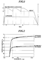
- FIG. 2 is an explanation view showing the light transmission of the ZnTe single crystal substrate before and after the heat treatment of this embodiment.
- the ZnTe single crystal substrate which was obtained after the heat treatment had the light transmission of 50% or more to the light beam having a wavelength of 700nm or more.
- the ZnTe single crystal substrate which was prepared before the heat treatment had the light transmission of about 30% to the light beam having a wavelength of 700nm or more.
- the light transmission equal to the above-described ones were obtained regardless of the thickness. Because it is considered that the reduction in the light transmission is mainly caused by the reflection at the surface and light hardly absorbed by the ZnTe single crystal, it can be easily assumed that the similar light transmission also can be obtained by a ZnTe single crystal substrate having a thickness of 4.0mm or more.
- FIG. 3 is explanation views showing the result of the observation of the ZnTe single crystal substrate before and after the heat treatment of this embodiment by a transmission type of optical microscope.
- FIG. 3(a) shows the observation result of the ZnTe single crystal substrate before the heat treatment.
- FIG. 3(b) shows the observation result of the ZnTe single crystal substrate after the heat treatment.
- Te deposits were scattered in the substrate before the heat treatment. It was confirmed by observing the cross section of the substrate that Te deposits having sizes of 2 ⁇ m or more and having a density of 10 5 cm -3 or more remained in the substrate.
- FIG. 3(b) it was confirmed that no Te deposit having a size of 2 ⁇ m or more remained in the substrate obtained after the heat treatment.
- Te deposits in the ZnTe single crystal substrate can be effectively eliminated and the light transmission can be 50% or more to the light beam having a wavelength of 700nm or more.
- the ZnTe single crystal substrate as described above, it is possible to realize a light modulation element having a superior characteristic.
- the present invention is specifically described based on the embodiment.
- the present invention is not limited to the above embodiment.
- the first heat treatment temperature T1 was 850 °C in the above embodiment
- a ZnTe single crystal substrate having a similar light transmission can be obtained by setting the first heat treatment temperature T1 in a range of 700 to 1250 °C.
- the heat treatment time (retention time) of the first step and the heat treatment time (temperature reducing rate) of the second step are not particularly limited and can be appropriately changed.
- the second heat treatment temperature T2 was set to be lower than the first heat treatment temperature T1 by 60 °C in the above embodiment, the second heat treatment temperature T2 may be set to be lower than the first heat treatment temperature T1 by 50 °C or more.
- the second heat treatment temperature T2 may be a room temperature, the second heat treatment temperature T2 is preferably (T1-200) °C or more and more preferably (T1-100) °C or more from the industrial viewpoint.
- the present invention is a technique for a heat treatment method of a ZnTe single crystal substrate. However, it is considered that the present invention is effective to reduce deposits in crystals of general II-VI group compound semiconductors other than ZnTe.
Landscapes
- Chemical & Material Sciences (AREA)
- Engineering & Computer Science (AREA)
- Crystallography & Structural Chemistry (AREA)
- Materials Engineering (AREA)
- Metallurgy (AREA)
- Organic Chemistry (AREA)
- Inorganic Chemistry (AREA)
- Physics & Mathematics (AREA)
- Thermal Sciences (AREA)
- Crystals, And After-Treatments Of Crystals (AREA)
Abstract
Description
- The present invention relates to a technique for improving the crystallinity of a II-VI group compound semiconductor single crystal suitable for a substrate for a light modulation element. In particular, the present invention relates to a heat treatment technique for eliminating deposits included in a ZnTe single crystal to improve the light transmission.
- Because a compound semiconductor crystal comprising the 12 (2B) group element and the 16 (6B) group element in the periodic table (hereinafter referred to as a II-VI group compound semiconductor) has various forbidden band widths, the crystal has various optical characteristics. Further, the II-VI group compound semiconductor has been expected to be used as material for a light modulation element for example. However, in case of the II-VI group compound semiconductor, because it is difficult to control the stoichiometric composition (stoichiometry), it is difficult to grow a good bulk crystal by the traditional manufacture technique.
- For example, in ZnTe, a composition at the melting point is shifted to Te from the stoichiometric composition. Thus, in grown crystals, there is some possibility that deposits that are presumably caused by excessive Te, remain. Because the Te deposits have sizes of a few µm and densities of about 105cm-3, the Te deposits are a cause of a remarkable decrease in the light transmission of a ZnTe single crystal substrate. The ZnTe single crystal substrate having such a low light transmission is not suitable for a light modulation element or the like using an electro-optic effect, in which laser light passes through a crystal having a thickness of about 10mm.
- As a technique for reducing the deposits in the ZnTe single crystal, there is a method for growing the ZnTe single crystal by using epitaxial growth technique. According to this technique, it is possible to manufacture a ZnTe single crystal having a superior crystallinity.
- The present applicant has suggested a method for manufacturing a II-VI group compound semiconductor single crystal that comprises at least: a first step of increasing a temperature of a II-VI group compound semiconductor single crystal to a first heat treatment temperature T1 and retaining the temperature of the crystal for a predetermined time; and a second step of gradually reducing the temperature of the crystal from the first heat treatment temperature T1 to a second heat treatment temperature T2 lower than the heat treatment temperature T1 with a predetermined rate (Patent Publication 1) . According to the invention disclosed in Patent Publication 1, in the first step, it is possible to eliminate the deposits consisting of the 16 group element (e.g., Te) and in the second step, it is possible to eliminate the deposits consisting of polycrystal and the like.
- Patent Publication 1:
Japanese Laid-Open Publication No. 2004-158731 - However, although the above epitaxial growth technique is effective for growing a ZnTe single crystal having a relatively thin thickness (e.g., about a few µm), excessive time and cost is required when a ZnTe single crystal having a thickness of 1mm or more is grown. This technique is not a realistic option.
- Furthermore, although the above heat treatment method disclosed in Patent Publication 1 can eliminate the Te deposits in a ZnTe single crystal substrate having a thickness up to 1mm and is effective, it was found that this method was not always effective for a substrate having a thickness of 1mm or more used for a light modulation element or the like because there were some cases that a heat treatment effect was not sufficiently obtained.
- Specifically, in case that the thickness of the ZnTe single crystal substrate is 1mm or more, when a heat treatment process (the first step + the second step) was carried out for about 100 hours in consideration of productivity in the above-described heat treatment method of Patent Publication 1, the ZnTe single crystal substrate obtained after the heat treatment had a light transmission (at a wavelength of 1000nm) of 50% or less, and was not suitable for an application for a light modulation element or the like. The cross section of the ZnTe single crystal substrate was also observed by an optical microscope. In the cross section, no deposits was shown in a region having a depth of about 0.20mm from the surface. However, in a further inner region, Te deposits having sizes of 3 to 10µm remained and the densities thereof were the same as that of the crystal before the heat treatment.
- In order for a ZnTe single crystal substrate having a thickness of 1mm or more to have a light transmission (wavelength: 1000nm) of 50% or more by using the heat treatment method disclosed in Patent Publication 1, it is required that a heat treatment is carried out for 200 hours or more depending on the heat treatment temperature. It was clear that the productivity was remarkably deteriorated.
- Thus, the present inventors considered that the heat treatment method according to the above prior application is effective for eliminating Te deposits but can be further improved. Thus, the present inventors have keenly studied the heat treatment method of a ZnTe compound semiconductor single crystal.
- It is an object of the present invention to provide a heat treatment method for effectively eliminating Te deposits in a ZnTe single crystal substrate and a ZnTe single crystal substrate having a thickness of 1mm or more that has an optical characteristic suitable for a light modulation element or the like.
- The present invention is a heat treatment method of a ZnTe single crystal substrate, comprising: a first step of increasing a temperature the ZnTe single crystal substrate to a first heat treatment temperature T1, and retaining the temperature of the substrate for a predetermined time; and a second step of gradually reducing the temperature of the substrate from the first heat treatment temperature T1 to a second heat treatment temperature T2 lower than the heat treatment temperature T1 with a predetermined rate, wherein the first heat treatment temperature T1 is set in a range of 700 °C≤T1≤1250 °C and the second heat treatment temperature T2 is set in a range of T2≤T1-50.
- The first and second steps are performed in a Zn atmosphere of at least 1 kPa or more. In particular, this method is effective for the ZnTe single crystal substrate having a thickness of 1mm or more, which is used for a light modulation element or the like. When the first and second steps are assumed as a cycle, the first and second steps may be repeated predetermined cycle number of times.
- In a ZnTe single crystal substrate for a light modulation element according to the present invention, when the substrate has a thickness of 1mm or more, deposits included in a crystal have sizes of 2µm or less and have densities of lower than 200cm-3. The above ZnTe single crystal substrate has a light transmission of 50% or more to light beam having a wavelength of 700nm to 1500nm. In particular, the ZnTe single crystal substrate has a light transmission of 60% or more to light beam having a wavelength of 900nm to 1500nm. By the above heat treatment method according to the present invention, it is possible to provide the ZnTe single crystal substrate as described above.
- The following section will describe how the present invention was completed.
First, when the present inventors applied a ZnTe single crystal substrate having a thickness of 2mm or more used for a light modulation element or the like to the above heat treatment method disclosed in Patent Publication 1, the above-described problem was found. In order to solve the above problem, the above heat treatment method disclosed in Patent Publication 1 was used and the present inventors studied the heat treatment conditions. - Specifically, the temperature of a ZnTe single crystal substrate was increased to the first heat treatment temperature T1 with a predetermined rate (e.g. , 15 °C /min) and the temperature of the substrate for a predetermined time (e. g. , 2 hours) (the first step). Thereafter, the temperature of the substrate was gradually reduced with a predetermined rate (e. g. , 0.3 °C/min) to the second heat treatment temperature T2 lower than the first heat treatment temperature T1 by 60 °C (the second step). Then, when the first step and second step were assumed as a cycle (about 5.4 hour), the first step and the second step were carried out for the ZnTe single crystal substrate predetermined cycle number of times.
- In the case of the heat treatment method in which a heat treatment was carried out for a ZnTe single crystal substrate in a Zn atmosphere to reduce deposits according to the above prior application, it was considered that the heat treatment time depended on a Zn diffusion speed. Therefore, Te deposits remaining in a ZnTe single crystal substrate after the heat treatment were investigated by using the heat treatment time (cycle number) and the temperature as parameters. In order to confirm a Zn diffusion effect due to the heat treatment, a relatively thick ZnTe single crystal substrate having a thickness of about 4mm was used.
- Specifically, a heat treatment was carried out for the ZnTe single crystal substrate at the first heat treatment temperatures T1 of 650 °C, 750 °C, and 850 °C and for heat treatment time (cycle number) of 54 hours (10 cycles), 108 hours (20 cycles), and 216 hours (40 cycles).
- In the above prior application, the first heat treatment temperature T1 was in a range of 0.5M≤T1≤0.65M (M: melting point). That is, when a melting point of ZnTe is 1239°C, the first heat treatment temperature T1 is in a range of 619.5≤T1≤805.35.
- Table 1 shows a region in which deposits in the ZnTe single crystal substrate disappear after the above-described heat treatment by using the depth from the surface.
As shown in Table 1, in case that the first heat treatment temperature T1 was 650 °C, a region having no deposits was about 0.5mm from the surface even when the heat treatment time was 216 hours (40 cycle). On the other hand, in case that the first heat treatment temperature T1 was 750 °C, a region having no deposits was 0. 9mm from the surface when the heat treatment time was 108 hours (20 cycles). In case that the first heat treatment temperature T1 was 850 °C, deposit perfectly disappeared when the heat treatment time was 108 hours (20 cycles). Because Zn diffuses from both faces of the substrate, it was found that a region in which deposits disappeared was 2.0mm or more when the region was representing by using the depth from the surface. -
[Table 1] Heat treatment time 54 hours (10 cycles) 108 hours (20 cycles) 216 hours (40 cycles) T1/T2 650/590(°C) 0.2mm 0.3mm 0.5mm 750/690(°C) - 0.9mm 1.5mm 850/690(°C) 1.5mm 2.0mm or more - - Then, in the ZnTe single crystal substrates for which the above heat treatments were carried out, the light transmission was investigated when light beam having a wavelength of 700nm to 1500nm was irradiated to the ZnTe single crystal substrates.
As a result, a ZnTe single crystal substrate in which deposits substantially disappeared when the first heat treatment temperature T1 was 850 °C and the heat treatment time was 108 hours (20 cycles), had a light transmission of 50% or more (at a wavelength of 700nm to 1500nm). Prior to the heat treatment, the substrate had a light transmission of 50% or less (at a wavelength 700nm to 1500nm). - Further, as a result of carrying out experiments, by carrying out the heat treatment at the first heat treatment temperature of 700 °C to 1250 °C for 20 cycles (108 hours) or more, it was found that the ZnTe single crystal substrate had light a transmission of 50% or more (at a wavelength 700nm to 1500nm). In particular, when the first heat treatment temperature was 850 °C or more, Te deposits perfectly disappeared by the heat treatment for 20 cycles. It was found that the substrate was suitable for a light modulation element.
- On the other hand, even when the first heat treatment temperature was lower than 700 °C, by carrying out a heat treatment for 216 hours (40 cycles), a substrate having a thickness of about 2mm had light transmission of 50% or more (at a wavelength 700nm to 1500nm). However, the conditions were not appropriate as heat treatment conditions from the viewpoint of productivity.
- From the above experiment result, the present invention was achieved based on a finding that by carrying out the heat treatment for a ZnTe single crystal substrate at the first heat treatment temperature T1 of 700 to 1250 °C and the second heat treatment temperature of (T1-50) or less, it was possible to effectively eliminate Te deposit part without remarkably deteriorating the productivity and to improve the light transmission of the ZnTe single crystal substrate.
- According to the present invention, in the heat treatment method of a ZnTe single crystal substrate, comprises: a first step of increasing a temperature the ZnTe single crystal substrate to a first heat treatment temperature T1, and retaining the temperature of the substrate for a predetermined time; and a second step of gradually reducing the temperature of the substrate from the first heat treatment temperature T1 to a second heat treatment temperature T2 lower than the heat treatment temperature T1 with a predetermined rate, wherein the first heat treatment temperature T1 is set in a range of 700 °C≤T1≤1250 °C and the second heat treatment temperature T2 is set in a range of T2≤T1-50. Therefore, it is possible that deposits in the ZnTe single crystal substrate effectively disappear and that a ZnTe single crystal substrate having a high light transmission is obtained.
- According to the ZnTe single crystal substrate for a light modulation element, which is obtained by the above heat treatment method, wherein when the substrate has a thickness of 1mm or more, deposits included in a crystal have sizes of 2µm or less and have densities of lower than 200cm-3 and wherein ZnTe single crystal substrate has a light transmission of 50% or more to light beam having a wavelength of 700nm to 1500nm, an effect that the a light modulation element having a superior characteristic is realized by using the ZnTe single crystal substrate, can be obtained.
-
- [
FIG. 1 ] This is an explanation view showing a temperature profile a heat treatment for which a ZnTe single crystal substrate is carried out in an embodiment. - [
FIG. 2 ] This is an explanation view showing the light transmission of the ZnTe single crystal substrate before and after the heat treatment in the embodiment. - [
FIG. 3 ] These are explanation views showing the surface status (Te deposit) of the ZnTe single crystal substrate before and after the heat treatment in the embodiment. - Hereinafter, a preferred embodiment of the present invention will be described.
In this embodiment, a sample obtained by the following method (substrate) was used. A ZnTe single crystal substrate having a diameter of 2 to 3 inches and having a plane orientation of (100) or (110) was obtained by a melt growth using gallium (Ga) as a dopant. The obtained substrate is sliced so as to have a thickness of 0.7 to 4.0mm. The wrapping using #1200 abrasive grain and the etching using Br23%MeOH were carried out for the surface of the sliced substrate to use it as the sample (substrate). - Before the heat treatment for the ZnTe single crystal substrate, the ZnTe single crystal substrate and Zn were placed at a predetermined position in a quartz ampule and the ampule was sealed at a vacuum degree of 1.0Pa or less. Then, the quartz ampule was placed in a diffusion furnace to perform the following heat treatment.
- The heat treatment according to this embodiment was performed in accordance with the temperature profile of
FIG. 1 . Specifically, a part at which the ZnTe single crystal substrate was placed was heated to the first heat treatment temperature T1= of 850 °C with a rate of 15 °C/min for example and the temperature was retained at 850 °C for 2 hours (the first step). A part at which Zn was placed was heated so that a Zn pressure P was 1.0kPa or more. - Next, the temperature of the substrate was gradually reduced with a rate of 0.3 °C/min to the second heat treatment temperature T2 of 790 °C (T2≤T1-50) (the second step). Specifically, the heat treatment time in the second step was 60/0.3= 200 minutes.
- Then, when the heat treatment comprising the above-described first and second steps, that is, the process in which the temperature of the ZnTe single crystal is increased to the first heat treatment temperature T1, the temperature of the substrate is retained for 2 hours and then the temperature of the substrate is reduced to the second heat treatment temperature T2, is assumed as one cycle (about 5.4 hours), the process was repeated 20 cycles (about 108 hours).
- Thereafter, the temperature of the part at which the ZnTe single crystal substrate was placed was reduced to a room temperature with a rate of 15 °C/min for example, and the heat treatment was completed. The temperature of the part at which Zn was placed was similarly reduced to the room temperature.
- Then, the wrapping and etching processing was carried out for the ZnTe single crystal substrate which was obtained after the heat treatment, under the conditions which were the same as those of the previous processing. Then, the light transmission of the substrate was measured and the status of the surface was observed.
-
FIG. 2 is an explanation view showing the light transmission of the ZnTe single crystal substrate before and after the heat treatment of this embodiment. As shown inFIG. 2 , the ZnTe single crystal substrate which was obtained after the heat treatment had the light transmission of 50% or more to the light beam having a wavelength of 700nm or more. On the other hand, the ZnTe single crystal substrate which was prepared before the heat treatment had the light transmission of about 30% to the light beam having a wavelength of 700nm or more. Thus, it was confirmed that the light transmission was remarkably improved by carrying out the heat treatment according to this embodiment. - In case of any of the ZnTe single crystal substrates having a thickness of 0.7 to 4.0mm, the light transmission equal to the above-described ones were obtained regardless of the thickness. Because it is considered that the reduction in the light transmission is mainly caused by the reflection at the surface and light hardly absorbed by the ZnTe single crystal, it can be easily assumed that the similar light transmission also can be obtained by a ZnTe single crystal substrate having a thickness of 4.0mm or more.
-
FIG. 3 is explanation views showing the result of the observation of the ZnTe single crystal substrate before and after the heat treatment of this embodiment by a transmission type of optical microscope.FIG. 3(a) shows the observation result of the ZnTe single crystal substrate before the heat treatment. FIG. 3(b) shows the observation result of the ZnTe single crystal substrate after the heat treatment. As shown inFIG. 3(a) , Te deposits were scattered in the substrate before the heat treatment. It was confirmed by observing the cross section of the substrate that Te deposits having sizes of 2µm or more and having a density of 105cm-3 or more remained in the substrate. On the other hand, as shown in FIG. 3(b), it was confirmed that no Te deposit having a size of 2µm or more remained in the substrate obtained after the heat treatment. - As described above, in accordance with the heat treatment method according to this embodiment, Te deposits in the ZnTe single crystal substrate can be effectively eliminated and the light transmission can be 50% or more to the light beam having a wavelength of 700nm or more. Thus, by using the ZnTe single crystal substrate as described above, it is possible to realize a light modulation element having a superior characteristic.
- As described above, the invention made by the present inventors is specifically described based on the embodiment. However, the present invention is not limited to the above embodiment.
For example, although the first heat treatment temperature T1 was 850 °C in the above embodiment, a ZnTe single crystal substrate having a similar light transmission can be obtained by setting the first heat treatment temperature T1 in a range of 700 to 1250 °C. - Furthermore, the heat treatment time (retention time) of the first step and the heat treatment time (temperature reducing rate) of the second step are not particularly limited and can be appropriately changed.
- Although the second heat treatment temperature T2 was set to be lower than the first heat treatment temperature T1 by 60 °C in the above embodiment, the second heat treatment temperature T2 may be set to be lower than the first heat treatment temperature T1 by 50 °C or more. Although the second heat treatment temperature T2 may be a room temperature, the second heat treatment temperature T2 is preferably (T1-200) °C or more and more preferably (T1-100) °C or more from the industrial viewpoint.
- The present invention is a technique for a heat treatment method of a ZnTe single crystal substrate. However, it is considered that the present invention is effective to reduce deposits in crystals of general II-VI group compound semiconductors other than ZnTe.
Claims (7)
- A heat treatment method of a ZnTe single crystal substrate, comprising:a first step of increasing a temperature the ZnTe single crystal substrate to a first heat treatment temperature T1, and retaining the temperature of the substrate for a predetermined time; anda second step of gradually reducing the temperature of the substrate from the first heat treatment temperature T1 to a second heat treatment temperature T2 lower than the heat treatment temperature T1 with a predetermined rate,wherein the first heat treatment temperature T1 is set in a range of 700 °C≤T1≤1250 °C and the second heat treatment temperature T2 is set in a range of T2≤T1-50.
- The heat treatment method of the ZnTe single crystal substrate as claimed in claim 1, wherein:the first and second steps are performed in a Zn atmosphere of at least 1 kPa or more.
- The heat treatment method of the ZnTe single crystal substrate as claimed in claim 1 or 2, wherein:the ZnTe single crystal substrate has a thickness of 1mm or more.
- The heat treatment method of the ZnTe single crystal substrate as claimed in any one of claims 1 to 3, wherein:when the first and second steps are assumed as a cycle, the first and second steps are repeated predetermined cycle number of times.
- A ZnTe single crystal substrate for a light modulation element, wherein when the substrate has a thickness of 1mm or more, deposits included in a crystal have sizes of 2µm or less and have densities of lower than 200cm-3.
- The ZnTe single crystal substrate for the light modulation element as claimed in claim 5, wherein:the ZnTe single crystal substrate has a light transmission of 50% or more to light beam having a wavelength of 700nm to 1500nm.
- The ZnTe single crystal substrate for the light modulation element as claimed in claim 6, wherein:the ZnTe single crystal substrate has a light transmission of 60% or more to light beam having a wavelength of 900nm to 1500nm.
Applications Claiming Priority (2)
| Application Number | Priority Date | Filing Date | Title |
|---|---|---|---|
| JP2005211011 | 2005-07-21 | ||
| PCT/JP2006/314157 WO2007010890A1 (en) | 2005-07-21 | 2006-07-18 | HEAT TREATMENT METHOD FOR ZnTe SINGLE CRYSTAL SUBSTRATE AND ZnTe SINGLE CRYSTAL SUBSTRATE |
Publications (3)
| Publication Number | Publication Date |
|---|---|
| EP1905873A1 true EP1905873A1 (en) | 2008-04-02 |
| EP1905873A4 EP1905873A4 (en) | 2008-09-10 |
| EP1905873B1 EP1905873B1 (en) | 2012-02-01 |
Family
ID=37668770
Family Applications (1)
| Application Number | Title | Priority Date | Filing Date |
|---|---|---|---|
| EP06781178A Ceased EP1905873B1 (en) | 2005-07-21 | 2006-07-18 | HEAT TREATMENT METHOD FOR ZnTe SINGLE CRYSTAL SUBSTRATE AND ZnTe SINGLE CRYSTAL SUBSTRATE |
Country Status (6)
| Country | Link |
|---|---|
| US (2) | US8476171B2 (en) |
| EP (1) | EP1905873B1 (en) |
| JP (1) | JP5032319B2 (en) |
| CN (2) | CN101228300B (en) |
| RU (1) | RU2411311C2 (en) |
| WO (1) | WO2007010890A1 (en) |
Family Cites Families (6)
| Publication number | Priority date | Publication date | Assignee | Title |
|---|---|---|---|---|
| JPH1112078A (en) * | 1997-06-16 | 1999-01-19 | Japan Energy Corp | Method for manufacturing compound semiconductor single crystal |
| US6791257B1 (en) | 1999-02-05 | 2004-09-14 | Japan Energy Corporation | Photoelectric conversion functional element and production method thereof |
| JP4562223B2 (en) * | 1999-08-05 | 2010-10-13 | 日鉱金属株式会社 | Semiconductor single crystal heat treatment method and semiconductor device manufacturing method |
| RU2170291C1 (en) * | 2000-03-03 | 2001-07-10 | Научно-технологический центр радиационного приборостроения Научно-технологического концерна "Институт монокристаллов" НАН Украины | Method of preparing n-type selenide-based semiconductor material |
| WO2002081789A1 (en) | 2001-04-04 | 2002-10-17 | Nikko Materials Co., Ltd. | METHOD FOR MANUFACTURING ZnTe COMPOUND SEMICONDUCTOR SINGLE CRYSTAL ZNTE COMPOUND SEMICONDUCTOR SINGLE CRYSTAL, AND SEMICONDUCTOR DEVICE |
| JP4614616B2 (en) * | 2002-11-08 | 2011-01-19 | Jx日鉱日石金属株式会社 | ZnTe single crystal and method for producing the same |
-
2006
- 2006-07-18 JP JP2007526009A patent/JP5032319B2/en not_active Expired - Fee Related
- 2006-07-18 WO PCT/JP2006/314157 patent/WO2007010890A1/en not_active Ceased
- 2006-07-18 US US11/988,755 patent/US8476171B2/en active Active
- 2006-07-18 CN CN200680026704XA patent/CN101228300B/en active Active
- 2006-07-18 EP EP06781178A patent/EP1905873B1/en not_active Ceased
- 2006-07-18 CN CN201110280113.8A patent/CN102352536B/en active Active
- 2006-07-18 RU RU2008106608/05A patent/RU2411311C2/en active
-
2011
- 2011-06-13 US US13/158,618 patent/US20110236297A1/en not_active Abandoned
Non-Patent Citations (3)
| Title |
|---|
| See also references of WO2007010890A1 * |
| UCHIDA M ET AL: "Stoichiometry control of ZnTe single crystals by the vapor pressure-controlled wafer-annealing method" JOURNAL OF CRYSTAL GROWTH, ELSEVIER, AMSTERDAM, NL, vol. 216, no. 1-4, 1 June 2000 (2000-06-01), pages 134-140, XP004206229 ISSN: 0022-0248 * |
| YABE T; ASAHI T; SATO K: "REduction of Te inclusion in ZnTe single crystals by thermal annealing" PHYSICA STATUS SOLIDI C, no. 4, 2004, pages 921-924, XP002483126 * |
Also Published As
| Publication number | Publication date |
|---|---|
| JPWO2007010890A1 (en) | 2009-01-29 |
| WO2007010890A1 (en) | 2007-01-25 |
| CN101228300A (en) | 2008-07-23 |
| RU2008106608A (en) | 2009-08-27 |
| CN102352536A (en) | 2012-02-15 |
| US20110236297A1 (en) | 2011-09-29 |
| US20090042002A1 (en) | 2009-02-12 |
| JP5032319B2 (en) | 2012-09-26 |
| US8476171B2 (en) | 2013-07-02 |
| EP1905873B1 (en) | 2012-02-01 |
| EP1905873A4 (en) | 2008-09-10 |
| CN102352536B (en) | 2015-09-09 |
| CN101228300B (en) | 2012-10-10 |
| RU2411311C2 (en) | 2011-02-10 |
Similar Documents
| Publication | Publication Date | Title |
|---|---|---|
| KR101581044B1 (en) | Method of prepairing a substrate having near perfect crystal thin layers | |
| US7713847B2 (en) | Method for forming AlGaN crystal layer | |
| EP2245218B1 (en) | Method for producing group iii nitride wafers and group iii nitride wafers | |
| EP1029368A1 (en) | Semiconductor substrate and method for making the same | |
| EP0856600B1 (en) | LiGa02 single crystal, single-crystal substrate, and method of manufacturing the same | |
| DE19781541B4 (en) | Device of a III-V compound semiconductor and method of manufacturing the device | |
| EP1533402B1 (en) | Epitaxial wafer and its manufacturing method | |
| EP1905873B1 (en) | HEAT TREATMENT METHOD FOR ZnTe SINGLE CRYSTAL SUBSTRATE AND ZnTe SINGLE CRYSTAL SUBSTRATE | |
| US7615470B2 (en) | Method of manufacturing gallium nitride semiconductor | |
| JPH04233219A (en) | Manufacture of products comprising semiconductor devices | |
| KR100519326B1 (en) | method for fabricating substate of GaN semiconductor laser diode | |
| EP3435407A1 (en) | Method for producing group iii nitride laminate | |
| US4595423A (en) | Method of homogenizing a compound semiconductor crystal prior to implantation | |
| JP2000269143A (en) | Method for producing gallium nitride-based compound semiconductor crystal | |
| TWI922927B (en) | Diamond substrate and method of manufacturing the same | |
| JP4614616B2 (en) | ZnTe single crystal and method for producing the same | |
| EP4317547A1 (en) | Ga2o3-based single crystal substrate and method for manufacturing ga2o3-based single crystal substrate | |
| JP3065078B1 (en) | II-VI compound semiconductor crystal and heat treatment method | |
| JP2003146791A (en) | Method for producing compound semiconductor single crystal | |
| JPS6355195A (en) | Method for growing inorganic compound single crystal | |
| JP2023145595A (en) | Indium phosphide substrate and semiconductor epitaxial wafer | |
| JPH0745360B2 (en) | InP single crystal heat treatment method | |
| JPH01194314A (en) | Method for growing thin film crystal | |
| JPH06293600A (en) | Production of impurity-doped semiconductor crystal | |
| JPH02112236A (en) | Manufacture of compound semiconductor device |
Legal Events
| Date | Code | Title | Description |
|---|---|---|---|
| PUAI | Public reference made under article 153(3) epc to a published international application that has entered the european phase |
Free format text: ORIGINAL CODE: 0009012 |
|
| 17P | Request for examination filed |
Effective date: 20080208 |
|
| AK | Designated contracting states |
Kind code of ref document: A1 Designated state(s): DE FR GB |
|
| DAX | Request for extension of the european patent (deleted) | ||
| A4 | Supplementary search report drawn up and despatched |
Effective date: 20080618 |
|
| 16A | New documents despatched to applicant after publication of the search report |
Effective date: 20080812 |
|
| RA4 | Supplementary search report drawn up and despatched (corrected) |
Effective date: 20080810 |
|
| DAX | Request for extension of the european patent (deleted) | ||
| RBV | Designated contracting states (corrected) |
Designated state(s): DE FR GB |
|
| 17Q | First examination report despatched |
Effective date: 20090114 |
|
| GRAP | Despatch of communication of intention to grant a patent |
Free format text: ORIGINAL CODE: EPIDOSNIGR1 |
|
| GRAS | Grant fee paid |
Free format text: ORIGINAL CODE: EPIDOSNIGR3 |
|
| GRAA | (expected) grant |
Free format text: ORIGINAL CODE: 0009210 |
|
| AK | Designated contracting states |
Kind code of ref document: B1 Designated state(s): DE FR GB |
|
| REG | Reference to a national code |
Ref country code: GB Ref legal event code: FG4D |
|
| REG | Reference to a national code |
Ref country code: DE Ref legal event code: R096 Ref document number: 602006027443 Country of ref document: DE Effective date: 20120329 |
|
| PLBE | No opposition filed within time limit |
Free format text: ORIGINAL CODE: 0009261 |
|
| STAA | Information on the status of an ep patent application or granted ep patent |
Free format text: STATUS: NO OPPOSITION FILED WITHIN TIME LIMIT |
|
| 26N | No opposition filed |
Effective date: 20121105 |
|
| REG | Reference to a national code |
Ref country code: DE Ref legal event code: R097 Ref document number: 602006027443 Country of ref document: DE Effective date: 20121105 |
|
| REG | Reference to a national code |
Ref country code: GB Ref legal event code: 732E Free format text: REGISTERED BETWEEN 20130801 AND 20130807 |
|
| REG | Reference to a national code |
Ref country code: DE Ref legal event code: R081 Ref document number: 602006027443 Country of ref document: DE Owner name: JX NIPPON MINING & METALS CORP., JP Free format text: FORMER OWNER: NIPPON MINING & METALS CO., LTD., TOKIO/TOKYO, JP Effective date: 20130715 |
|
| REG | Reference to a national code |
Ref country code: FR Ref legal event code: CD Owner name: JX NIPPON MINING & METALS CORPORATION, JP Effective date: 20130819 Ref country code: FR Ref legal event code: TP Owner name: JX NIPPON MINING & METALS CORPORATION, JP Effective date: 20130819 Ref country code: FR Ref legal event code: CA Effective date: 20130819 |
|
| REG | Reference to a national code |
Ref country code: FR Ref legal event code: PLFP Year of fee payment: 11 |
|
| REG | Reference to a national code |
Ref country code: FR Ref legal event code: PLFP Year of fee payment: 12 |
|
| REG | Reference to a national code |
Ref country code: FR Ref legal event code: CA Effective date: 20171006 |
|
| REG | Reference to a national code |
Ref country code: FR Ref legal event code: PLFP Year of fee payment: 13 |
|
| PGFP | Annual fee paid to national office [announced via postgrant information from national office to epo] |
Ref country code: DE Payment date: 20240719 Year of fee payment: 19 |
|
| PGFP | Annual fee paid to national office [announced via postgrant information from national office to epo] |
Ref country code: GB Payment date: 20240722 Year of fee payment: 19 |
|
| PGFP | Annual fee paid to national office [announced via postgrant information from national office to epo] |
Ref country code: FR Payment date: 20240729 Year of fee payment: 19 |
|
| REG | Reference to a national code |
Ref country code: DE Ref legal event code: R082 Ref document number: 602006027443 Country of ref document: DE Representative=s name: DENNEMEYER & ASSOCIATES RECHTSANWALTSGESELLSCH, DE |
|
| REG | Reference to a national code |
Ref country code: DE Ref legal event code: R119 Ref document number: 602006027443 Country of ref document: DE |
|
| GBPC | Gb: european patent ceased through non-payment of renewal fee |
Effective date: 20250718 |
|
| PG25 | Lapsed in a contracting state [announced via postgrant information from national office to epo] |
Ref country code: GB Free format text: LAPSE BECAUSE OF NON-PAYMENT OF DUE FEES Effective date: 20250718 |
|
| PG25 | Lapsed in a contracting state [announced via postgrant information from national office to epo] |
Ref country code: DE Free format text: LAPSE BECAUSE OF NON-PAYMENT OF DUE FEES Effective date: 20260203 |
|
| PG25 | Lapsed in a contracting state [announced via postgrant information from national office to epo] |
Ref country code: FR Free format text: LAPSE BECAUSE OF NON-PAYMENT OF DUE FEES Effective date: 20250731 |