EP1901336A1 - Exposure apparatus - Google Patents
Exposure apparatus Download PDFInfo
- Publication number
- EP1901336A1 EP1901336A1 EP06732588A EP06732588A EP1901336A1 EP 1901336 A1 EP1901336 A1 EP 1901336A1 EP 06732588 A EP06732588 A EP 06732588A EP 06732588 A EP06732588 A EP 06732588A EP 1901336 A1 EP1901336 A1 EP 1901336A1
- Authority
- EP
- European Patent Office
- Prior art keywords
- light
- optical system
- projection optical
- exposure
- wavelength component
- Prior art date
- Legal status (The legal status is an assumption and is not a legal conclusion. Google has not performed a legal analysis and makes no representation as to the accuracy of the status listed.)
- Granted
Links
Images




Classifications
-
- G—PHYSICS
- G03—PHOTOGRAPHY; CINEMATOGRAPHY; ANALOGOUS TECHNIQUES USING WAVES OTHER THAN OPTICAL WAVES; ELECTROGRAPHY; HOLOGRAPHY
- G03F—PHOTOMECHANICAL PRODUCTION OF TEXTURED OR PATTERNED SURFACES, e.g. FOR PRINTING, FOR PROCESSING OF SEMICONDUCTOR DEVICES; MATERIALS THEREFOR; ORIGINALS THEREFOR; APPARATUS SPECIALLY ADAPTED THEREFOR
- G03F7/00—Photomechanical, e.g. photolithographic, production of textured or patterned surfaces, e.g. printing surfaces; Materials therefor, e.g. comprising photoresists; Apparatus specially adapted therefor
- G03F7/70—Microphotolithographic exposure; Apparatus therefor
- G03F7/70216—Mask projection systems
- G03F7/70258—Projection system adjustments, e.g. adjustments during exposure or alignment during assembly of projection system
-
- G—PHYSICS
- G03—PHOTOGRAPHY; CINEMATOGRAPHY; ANALOGOUS TECHNIQUES USING WAVES OTHER THAN OPTICAL WAVES; ELECTROGRAPHY; HOLOGRAPHY
- G03F—PHOTOMECHANICAL PRODUCTION OF TEXTURED OR PATTERNED SURFACES, e.g. FOR PRINTING, FOR PROCESSING OF SEMICONDUCTOR DEVICES; MATERIALS THEREFOR; ORIGINALS THEREFOR; APPARATUS SPECIALLY ADAPTED THEREFOR
- G03F7/00—Photomechanical, e.g. photolithographic, production of textured or patterned surfaces, e.g. printing surfaces; Materials therefor, e.g. comprising photoresists; Apparatus specially adapted therefor
- G03F7/70—Microphotolithographic exposure; Apparatus therefor
- G03F7/70216—Mask projection systems
- G03F7/70308—Optical correction elements, filters or phase plates for manipulating imaging light, e.g. intensity, wavelength, polarisation, phase or image shift
-
- G—PHYSICS
- G03—PHOTOGRAPHY; CINEMATOGRAPHY; ANALOGOUS TECHNIQUES USING WAVES OTHER THAN OPTICAL WAVES; ELECTROGRAPHY; HOLOGRAPHY
- G03F—PHOTOMECHANICAL PRODUCTION OF TEXTURED OR PATTERNED SURFACES, e.g. FOR PRINTING, FOR PROCESSING OF SEMICONDUCTOR DEVICES; MATERIALS THEREFOR; ORIGINALS THEREFOR; APPARATUS SPECIALLY ADAPTED THEREFOR
- G03F7/00—Photomechanical, e.g. photolithographic, production of textured or patterned surfaces, e.g. printing surfaces; Materials therefor, e.g. comprising photoresists; Apparatus specially adapted therefor
- G03F7/70—Microphotolithographic exposure; Apparatus therefor
- G03F7/70483—Information management; Active and passive control; Testing; Wafer monitoring, e.g. pattern monitoring
- G03F7/7055—Exposure light control in all parts of the microlithographic apparatus, e.g. pulse length control or light interruption
- G03F7/70575—Wavelength control, e.g. control of bandwidth, multiple wavelength, selection of wavelength or matching of optical components to wavelength
-
- G—PHYSICS
- G03—PHOTOGRAPHY; CINEMATOGRAPHY; ANALOGOUS TECHNIQUES USING WAVES OTHER THAN OPTICAL WAVES; ELECTROGRAPHY; HOLOGRAPHY
- G03F—PHOTOMECHANICAL PRODUCTION OF TEXTURED OR PATTERNED SURFACES, e.g. FOR PRINTING, FOR PROCESSING OF SEMICONDUCTOR DEVICES; MATERIALS THEREFOR; ORIGINALS THEREFOR; APPARATUS SPECIALLY ADAPTED THEREFOR
- G03F7/00—Photomechanical, e.g. photolithographic, production of textured or patterned surfaces, e.g. printing surfaces; Materials therefor, e.g. comprising photoresists; Apparatus specially adapted therefor
- G03F7/70—Microphotolithographic exposure; Apparatus therefor
- G03F7/708—Construction of apparatus, e.g. environment aspects, hygiene aspects or materials
- G03F7/70858—Environment aspects, e.g. pressure of beam-path gas, temperature
- G03F7/70883—Environment aspects, e.g. pressure of beam-path gas, temperature of optical system
- G03F7/70891—Temperature
Definitions
- the present invention relates to an exposure apparatus applied to a photolithography, such as to an exposure apparatus for extreme ultra violet lithography (EUVL) using an exposure wavelength of 50 nm or less.
- EUVL extreme ultra violet lithography
- the light-quantity sensors 12 and 13 are to be arranged in the luminous flux illuminating the region to be illuminated E' and incidents on the outside of the transfer region E.
- the light-quantity sensors 12 and 13 arranged in this place are able to monitor the light quantity of a luminous flux going to the wafer 7 without influencing the luminous flux.
- the wavelength-selecting filter F is made of, for example, zirconium, silicon, or the like, and has transmittivity only with respect to in-band light while blocking out-band light.
- the light-quantity sensor 12 is able to detect the light quantity of in-band light only.
- the detectable band of the light-quantity sensor 12 is, for example, as shown with the symbol E 12 in Fig. 3(b) .
- the curve in Fig. 3(b) is an example of the emission spectrum of the laser plasma light source 1a. Actually, the emission spectrum is not necessarily as this curve, and fluctuates according to the operating status of the laser plasma light source 1a.
- Fig. 4 is a flow chart of the operation of the controlling part 9 regarding the mirror adjusting system.
- the operation of the circuit portion and the operation of the computer portion of the controlling part 9 are represented without making any distinction between them. As shown in Fig.
- the heat-absorption coefficient for in-band light of a mirror Mi in the projection optical system 6 is represented by E i
- the heat-absorption coefficient for out-band light of the mirror M i in the projection optical system 6 is represented by V i .
- the controlling part 9 of this embodiment repeats adjustment similar to that of the first embodiment using the reticle side sensors 12 and 13 during an exposure period.
- the controlling part 9 of this embodiment corrects the heat-absorption coefficients (E1, V1, E2, V2, E3, V3, E4, V4, E5, V5, E6 and V6) of the projection optical system 6 using the wafer side sensors 12' and 13' for each appropriate time outside the exposure period.
- This correction is performed to address temporal changes in the reflection/absorption characteristics of the projection optical system 6, because there is a possibility that the reflectivities R1, R2, R3, R4, R5, and R6 of the mirrors M1, M2, M3, M4, M5, and M6 in the projection optical system 6 decrease with time due to contaminant generated in the projection exposure apparatus. In addition, contaminant is easier to adhere to mirrors on the upstream side, so that the temporal changes are remarkable.
- the fourth embodiment is different from the first embodiment in a method of calculating a heat-absorption amount at step S3 in Fig. 4 .
- the influence of light (returning light) which is reflected by the wafer 7 and then returns to the projection optical system 6 is neglected.
- the wafer 7 for EUVL does not reflect in-band light, and reflects out-band light, so that there is a possibility that the wafer 7 causes returning light (retuning light constituted by out-band light). In the calculation method of this embodiment, this is considered.
- the heat-absorption coefficient V i ' ( Fig. 14(B) ) is heat amount (heat-absorption amount) which is absorbed by the mirror M i due to the out-band light returning from the wafer when the quantity of out-band light incident on the projection optical system 6 is "one".
- the controlling part 9 of this embodiment estimates the heat-absorption amount W i of the mirror M i by applying the light quantity C of in-band light incident on the projection optical system 6 and the light quantity D of out-band light incident on the projection optical system 6 to the following equation (10).
Landscapes
- Physics & Mathematics (AREA)
- General Physics & Mathematics (AREA)
- Health & Medical Sciences (AREA)
- Life Sciences & Earth Sciences (AREA)
- Atmospheric Sciences (AREA)
- Toxicology (AREA)
- Engineering & Computer Science (AREA)
- Environmental & Geological Engineering (AREA)
- Epidemiology (AREA)
- Public Health (AREA)
- Exposure And Positioning Against Photoresist Photosensitive Materials (AREA)
- Exposure Of Semiconductors, Excluding Electron Or Ion Beam Exposure (AREA)
Abstract
Description
- The present invention relates to an exposure apparatus applied to a photolithography, such as to an exposure apparatus for extreme ultra violet lithography (EUVL) using an exposure wavelength of 50 nm or less.
- An ordinary exposure apparatus is equipped with light-quantity sensors for monitoring fluctuations in the light quantity of exposure light (see
patent documents 1 and 2, etc.). In particular, inpatent document 1, a system (lens adjusting system) is disclosed which arranges light-quantity sensors on an upstream side and a downstream side of a projection optical system, estimates fluctuation amounts of the characteristics of the projection optical system based on the outputs of the light-quantity sensors, and adjusts the projection optical system so as to control the fluctuation amounts. It is desirable that such an adjusting system be incorporated also in an exposure apparatus for EUVL which is a next-generation exposure apparatus.
Patent Document 1:Japanese Unexamined Patent Application Publication No. Hei9-36018
Patent Document 2:Japanese Unexamined Patent Application Publication No. Hei 11-16816 - However, the inventors of the present invention have found out that there is a possibility that the adjusting system does not operate normally when it is applied to an exposure apparatus for EUVL as it is. The reason is that a special light source for EUVL (EUV light source) is used in an exposure apparatus for EUVL, a special mirror for reflecting EUV light (reflecting mirror having a multilayered film) is used, and the like. In that case, it can be considered that it is difficult to estimate fluctuation amounts of the characteristics of a projection optical system from fluctuations in the light quantity of exposure light.
- It is therefore an object of the present invention to provide an exposure apparatus capable of accurately grasping characteristic fluctuations of an optical system caused by irradiation heat of light.
- First, the inventors of the present invention took the following circumstances peculiar to an exposure apparatus for EUV into consideration.
- [1] From an EUV light source, non-exposure wavelength components (out-band light) are emitted in addition to exposure wavelength components (in-band light) (the exposure wavelength components are EUV light, and the non-exposure wavelength components are extra ultraviolet light, visible light, infrared light, etc.).
- [2] It has been also studied to insert filters blocking out-band light. However, the filters must be inserted on the upstream as far as possible (on the upstream than an integrator of the illumination optical system). In that case, the filters are exposed to EUV light having a relatively large light quantity, so that a durability problem arises.
- [3] A reflecting mirror having a multilayered film used in many optical systems for EUVL reflects not only in-band light but also out-band light.
- [4] There is a high possibility that the light-quantity ratio between in-band light and out-band light fluctuates according to the operation status of an EUV light source.
- In view of the above circumstances, it is understood that at least it is necessary to detect in-band light and out-band light independently in order to accurately grasp characteristic fluctuations of an optical system for EUVL.
For this purpose, the exposure apparatus of the present invention is characterized in that an exposure apparatus exposing an object to be exposed with light emitted from a light source includes a detecting unit detecting light quantity of non-exposure wavelength component of the light. - The detecting unit preferably detects light quantity of exposure wavelength component of the light and light quantity of non-exposure wavelength component of the light independently.
Furthermore, any of the exposure apparatuses of the present invention preferably includes a projection optical system arranged between the light source and the object to be exposed, and an adjusting unit adjusting the projection optical system based on an output of the detecting unit. - Furthermore, the projection optical system preferably includes at least one mirror, and at least one of subjects of to be adjusted by the adjusting unit is preferably a position of the mirror in a direction perpendicular to an optical axis.
Furthermore, the projection optical system preferably includes at least one mirror, and at least one of subjects to be adjusted by the adjusting unit is preferably an attitude of the mirror.
Furthermore, the projection optical system preferably projects a pattern of a mask arranged on the light source side onto the object to be exposed, and at least one of subjects to be adjusted by the adjusting unit is preferably a relative position between the mask and the object to be exposed. - Furthermore, the projection optical system preferably projects a pattern of a mask arranged on the light source side onto the object to be exposed, and at least one of subjects to be adjusted by the adjusting unit is preferably an attitude of at least one of the mask and the object to be exposed.
Furthermore, the detecting unit preferably detects light quantity of exposure wavelength component of the light and light quantity of non-exposure wavelength component of the light independently, and the adjusting unit preferably determines, to carry out the adjusting, adjustment contents of the projection optical system based on light quantity of the exposure wavelength component, light quantity of the non-exposure wavelength component, characteristic information of the projection optical system for the exposure wavelength component, and characteristic information of the projection optical system for the non-exposure wavelength component. - Furthermore, the detecting unit preferably includes at least two of the detecting units, which are a first detecting unit whose detecting object is the light before passing the projection optical system, and a second detecting unit whose detecting object is the light after passing the projection optical system, and the adjusting unit preferably corrects characteristic information of the projection optical system for the exposure wavelength component based on light quantity of the exposure wavelength component detected by the first detecting unit and light quantity of the exposure wavelength component detected by the second detecting unit, and characteristic information of the projection optical system for the non-exposure wavelength component based on light quantity of the non-exposure wavelength component detected by the second detecting unit and light quantity of the non-exposure wavelength component detected by the second detecting unit.
- Furthermore, characteristic information of the projection optical system preferably includes each of absorption coefficients of optical members in the projection optical system.
Furthermore, the adjusting unit preferably reflects information about reflectivity of the object to be exposed for the non-exposure wavelength component into the adjustment contents.
Furthermore, any of the exposure apparatuses of the present invention may further include a detecting unit detecting reflectivity of the object to be exposed for the non-exposure wavelength component. - Furthermore, the detecting unit may include a sensor for exposure wavelength detecting light quantity of exposure wavelength component of the light, and a sensor for non-exposure wavelength detecting light quantity of non-exposure wavelength component of the light.
Furthermore, the detecting unit may include a sensor for specific wavelength detecting light quantity of exposure wavelength component or non-exposure wavelength component of the light, and a sensor for all wavelengths detecting light quantity of all wavelength components of the light. - Furthermore, the detecting unit may include a sensor for all wavelengths capable of detecting light quantity of all wavelength components of the light, and a switching unit switching wavelength of incident light on the sensor for all wavelengths between at least two of exposure wavelength, non-exposure wavelength, and all wavelengths.
Furthermore, the light source may be an EUV light source. - According to the present invention, an exposure apparatus capable of accurately grasping characteristic fluctuations of an optical system caused by irradiation heat of light is realized.
-
-
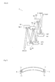
Fig. 1 is a schematic configuration diagram of a projection exposure apparatus of the first embodiment; -
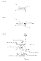
Fig. 2 illustrates in detail where light-quantity sensors -
Figs. 3(a) and 3(b) illustrate the configurations and detectable wavelength bands of light-quantity sensors -
Fig. 4 is a flow chart of the operation of a controllingpart 9 regarding a mirror adjusting system; -
Figs. 5(a) to 5(c) illustrate step S2; -
Fig. 6 illustrates step S3; -
Fig. 7 shows an example having two or more light-quantity sensors -
Fig. 8 is a schematic configuration diagram of a projection exposure apparatus of a second embodiment; -
Fig. 9 illustrates a variation of a sensor part; -
Fig. 10 illustrates another variation of a sensor part; -
Fig. 11 illustrates still another variation of a sensor part; -
Fig. 12 illustrates the degree of freedom of stages of a third embodiment; -
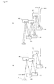
Figs. 1 3(A) and13(B) illustrate a method of determining adjusting amounts of the third embodiment; and -
Figs. 14(A) and 14(B) illustrate a method of calculating heat-absorption amounts of a fourth embodiment. - The first embodiment of the present invention will be described below with reference to
Figs. 1, 2 ,3 ,4 ,5 ,6, and 7 . This embodiment is an embodiment of a projection exposure apparatus for EUVL.
First, the configuration of the projection exposure apparatus will be described.
Fig. 1 is a schematic configuration diagram of the projection exposure apparatus. As shown inFig. 1 , in the projection exposure apparatus, anirradiating apparatus 1, an integrator of reflectingtype 3, acondenser mirror 4, an optical path bending mirror M, a reticle of reflectingtype 5, a reticle stage MS, a projection optical system of reflectingtype 6, awafer 7, a wafer stage WS, a mirror adjusting mechanism 8, light-quantity sensors part 9 consisting of a circuit, a computer, etc. Thereference numeral 100 inFig. 1 denotes a vacuum chamber for keeping all of the optical paths of the projection exposure apparatus in a vacuum. - The irradiating
apparatus 1 is equipped with a laser plasma light source 1a which is a kind of an EUV light source, and acollimator mirror 1e. From the laser plasma light source 1 a, EUV light of the wavelength of 13.5 nm which is in-band light, and out-band light of the other wavelengths are emitted.
Light emitted from the laser plasma light source a passes through thecollimator mirror 1e, theintegrator 3, thecondenser mirror 4, and the optical path bending mirror M in this order, and then illuminates the region to be illuminated of thereticle 5 evenly, Light reflected by the region to be illuminated of thereticle 5 enters the projectionoptical system 6. - In the projection
optical system 6, a plurality of mirrors, such as six mirrors M1, M2, M3, M4, M5, and M6 are arranged. Light reflected by the mirror M1, M2, M3, M4, M5, and M6 forms a reduced image of thereticle 5 on thewafer 7. The reduced image is a reduced image of a pattern formed in the region to be illuminated of thereticle 5. By the reduced image, a region to be exposed on the surface of thewafer 7 is exposed. - Distances between the mirrors M1, M2, M3, M4, M5, and M6 (positions in the optical axis directions of respective mirrors) in the projection
optical system 6 can be adjusted by the mirror adjusting mechanism 8. An instruction for the adjustment and adjusting amounts (adjusting amounts of respective mirrors in the optical axis directions) are given from thecontrolling part 9 to the mirror adjusting mechanism 8. Thus, the image-forming characteristic of the projectionoptical system 6 can be adjusted.
Here, to each of the optical systems in the projection exposure apparatus, a characteristic for reflecting in-band light (here, EUV light of the wavelength of 13.5 nm) has been added. In particular, each of the mirrors in theintegrator 3, thecondenser mirror 4, the optical path bending mirror M, and each of the mirrors M1, M2, M3, M4, M5, and M6 in the projectionoptical system 6, shown inFig. 1 , are direct incidence type mirrors the light incidence angles of which are less than 45 degrees, so that a multilayered film is formed on the reflecting surface of each of the mirrors. The multilayered film is formed by stacking two or more materials of, for example, molybdenum (Mo), silicon (Si), ruthenium (Ru), rhodium (Rh), silicon oxides, and the like. The reflectivity of a mirror on which such a multilayered film is formed is, for example, the order of about 60 to 70 % for in-band light, and the order of about 80 % for out-band light. - Next, the light-
quantity sensors
As shown inFig. 1 , arrangement places of the light-quantity sensors reticle 5. The arrangement places are shown in detail inFig. 2 . InFig. 2 , the symbol E' denotes a region to be illuminated of thereticle 5, and the symbol E denotes a transfer region of the reticle 5 (the transfer region is a region which is projected onto the wafer 7). The region to be illuminated E' covers the whole of the transfer region E and is slightly larger than the transfer region E. The light-quantity sensors quantity sensors wafer 7 without influencing the luminous flux. -
Figs. 3(a) and 3(b) illustrate the configurations and detectable wavelength bands of the light-quantity sensors
First, as shown on the left side ofFig. 3(a) , the light-quantity sensor 12 has a wavelength-selecting filter F provided on a photoelectric conversion element SA. The photoelectric conversion element SA is a photoelectric conversion element which consists of a silicon photodiode, etc., and senses light of a sufficiently wide wavelength band. The wavelength band sensed by the photoelectric conversion element SA covers the wavelength band (13.5 nm) of in-band light and the wavelength band of out-band light. The wavelength-selecting filter F is made of, for example, zirconium, silicon, or the like, and has transmittivity only with respect to in-band light while blocking out-band light. Thus, the light-quantity sensor 12 is able to detect the light quantity of in-band light only. The detectable band of the light-quantity sensor 12 is, for example, as shown with the symbol E12 inFig. 3(b) . The curve inFig. 3(b) is an example of the emission spectrum of the laser plasma light source 1a. Actually, the emission spectrum is not necessarily as this curve, and fluctuates according to the operating status of the laser plasma light source 1a. - Furthermore, as shown on the right side of
Fig. 3(a) , the light-quantity sensor 13 includes a photoelectric conversion element SA having the same characteristic as that used in the light-quantity sensor 12. Thus, the light-quantity sensor 13 is able to detect the sum of the light quantity of out-band light and the light quantity of in-band light. The detectable band of the light-quantity sensor 13 is, for example, as shown with the symbol E13 inFig. 3(b) .
Next, the mirror adjusting system of the projection exposure apparatus will be described. -
Fig. 4 is a flow chart of the operation of thecontrolling part 9 regarding the mirror adjusting system. InFig. 4 , the operation of the circuit portion and the operation of the computer portion of thecontrolling part 9 are represented without making any distinction between them.
As shown inFig. 4 , thecontrolling part 9 refers to the outputs of the light-quantity sensors 12 and 13 (step S1), calculates the light quantity of in-band light and the light quantity of out-band light incident on the projectionoptical system 6, independently, based on the outputs thereof (step S2), determines adjusting amounts of the projection optical system 6 (here, adjusting amounts in the optical axis directions of the mirrors) based on the calculated light-quantities (step S3), and gives an instruction for adjustment and adjusting amounts (here, adjusting amounts in the optical axis directions of the mirrors) to the mirror adjusting mechanism 8 to adjust projection optical system 6 (step S4). The steps S1 to S4 are executed repeatedly during the exposure period. The steps S2 and S3 will be described in detail below. - Now, it is assumed that the light quantity of in-band light incidents on the light-
quantity sensors quantity sensors Figs.5 (a) and (b) . Furthermore, the transmittance of the wavelength-selecting filter F in the light-quantity sensor 12 is represented by P, the sensitivity coefficient (conversion efficiency) for in-band light of the photoelectric conversion element SA is represented by S, and the sensitivity coefficient (conversion efficiency) for out-band light of the photoelectric conversion element SA is represented by T. - In the light-
quantity sensor 12, as shown inFig. 5(a) , in-band light having a light quantity A is attenuated by the transmittance P of the wavelength-selecting filter F and then enters the photoelectric conversion element SA to be converted to an electrical signal by the conversion efficiency S. On the other hand, out-band light having a light quantity B incident on the light-quantity sensor 12 is blocked by the wavelength-selecting filter F. Thus, the output X of the light-quantity sensor 12 is given by X = A × P × S. - Furthermore, in the light-
quantity sensor 13, as shown inFig. 5(b) , both of in-band light having a light quantity A and out-band light having a light quantity B enter the photoelectric conversion element SA without being attenuated at all. The in-band light is converted to an electrical signal by the conversion efficiency S, and the out-band light is converted to an electrical signal by the conversion efficiency T. Thus, the output Y of the light-quantity sensor 13 is given by Y = A × S + B × T. - Hence, the following equation (1) is derived.
-

Thus, thecontrolling part 9 calculates the light quantity A of the in-band light and the light quantity B of the out-band light independently by applying the output X of the light-quantity sensor 12 and the output Y of the light-quantity sensor 13 to the following equation (2). Information necessary for this calculation, that is, information about the characteristics of the light-quantity sensors controlling part 9 in advance. -

Note that the calculated light quantities A and B represent the light quantities of in-band light and out-band light which have entered the light-quantity sensors reticle 5.
Next, as shown inFig. 5(c) , when the reflection coefficient for in-band light of thereticle 5 is represented by G[R] and the reflection coefficient for out-band light of thereticle 5 is represented by H[R], the light quantity C of in-band light incident on the projectionoptical system 6 is given by C = A × G[R], and the light quantity D of out-band light incident on the projectionoptical system 6 is given by D = B × H[R]. In other words, the following equation (3) is derived. -

The reflection coefficients G[R] and H[R] are coefficients determined for each reticle ([R] represents a function of a reticle).
Thus, thecontrolling part 9 estimates the light quantity C of in-band light incident on the projectionoptical system 6 and the light quantity D of out-band light incident on the projectionoptical system 6 independently by applying the light quantities A and B to the above equation (3). - Note that, Information necessary for this estimation, that is, information about the characteristic of the
reticle 5 such as "G[R]" and "H[R]" is stored in thecontrolling part 9 in advance. - Now, as shown in
Fig. 6 , the heat-absorption coefficient for in-band light of a mirror Mi in the projectionoptical system 6 is represented by Ei, and the heat-absorption coefficient for out-band light of the mirror Mi in the projectionoptical system 6 is represented by Vi. However, the heat-absorption coefficient E; is a heat amount (heat-absorption amount) absorbed by the mirror Mi due to in-band light incident on the projectionoptical system 6 when the light quantity of the in-band light is "one", and the heat-absorption coefficient Vi is a heat amount (heat-absorption amount) absorbed by the mirror Mi due to out-band light incident on the projectionoptical system 6 when the light quantity of the out-band light is "one". In this specification, "heat-absorption amount of a mirror" means "light quantity of light changed to heat by a mirror", and is represented by light energy per unit time or the like. - When the light quantity of in-band light incident on the projection
optical system 6 is C, the heat-absorption amount wi of the mirror Mi caused by the in-band light is given by wi = C × Ei.
Furthermore, when the light quantity of out-band light incident on the projectionoptical system 6 is D, the heat-absorption amount wi' of the mirror Mi caused by the out-band light is given by wi' = D × Vi.
The sum of the heat-absorption amount wi of the mirror Mi caused by the in-band light and the heat-absorption amount wi' of the mirror Mi caused by the out-band light is a total heat-absorption amount Wi of the mirror Mi. - Thus, the
controlling part 9 estimates the heat-absorption amounts W1, W2, W3, W4, W5, and W6 of the mirrors M1, M2, M3, M4, M5, and M6 by applying the light quantity C of in-band light and the light quantity D of out-band light incident on the projectionoptical system 6 to the following equation (4). -

Note that, information necessary for this estimation, that is, information about the characteristics of the mirrors M1, M2, M3, M4, M5, and M6 such as "E1", "E2", "E3", "E4", "E5", "E6", "V1", "V2", "V3", "V4", "V5", and "V6" is stored in thecontrolling part 9 in advance. The heat-absorption coefficient Ei of the mirror Mi depends on the reflectivity for in-band light of the mirror Mi and the mirrors on the upstream side than it, and the heat-absorption coefficient Vi of the mirror Mi depends on the reflectivity for out-band light of the mirror Mi and the mirrors on the upstream side than it. - Further, the
controlling part 9 calculates the deformation rate P1 of the mirror M1 at this time point based on the heat-absorption amount W1 of themirror M 1 and the history of the heat-absorption amount (the deformation rate P1 can be calculated based on at least the heat-absorption amount W1 of the mirror M1 and the previous value of the heat-absorption amount. However, the content of the calculation depends on the time constant of the heat balance peculiar to the mirror M1). Note that, a deformation amount which becomes a basis of the deformation rate P1 is obtained when the mirror M1 has reached a steady state while the light quantity C of the in-band light and the light quantity D of the out-band light are being kept to reference values, respectively. - Likewise, the
controlling part 9 calculates the deformation rate P2 of the mirror M2 at this time point based on the heat-absorption amount W2 of the mirror M2 and the history of the heat-absorption amount (the deformation rate P2 can be calculated based on at least the heat-absorption amount W2 of the mirror M2 and the previous value of the heat-absorption amount. However, the content of the calculation depends on the time constant of the heat balance peculiar to the mirror M2). Note that, a deformation amount which becomes a basis of the deformation rate P2 is obtained when the mirror M2 has reached a steady state while the light quantity C of the in-band light and the light quantity D of the out-band light are being kept to reference values, respectively. - Likewise, the
controlling part 9 calculates the deformation rate P3 of the mirror M3 at this time point based on the heat-absorption amount W3 of the mirror M3 and the history of the heat-absorption amount (the deformation rate P3 can be calculated based on at least the heat-absorption amount W3 of the mirror M3 and the previous value of the heat-absorption amount. However, the content of the calculation depends on the time constant of the heat balance peculiar to the mirror M3). Note that, a deformation amount which becomes a basis of the deformation rate P3 is obtained when the mirror M3 has reached a steady state while the light quantity C of the in-band light and the light quantity D of the out-band light are being kept reference values, respectively. - Likewise, the
controlling part 9 calculates the deformation rate P4 of the mirror M4 at this time point based on the heat-absorption amount W4 of the mirror M4 and the history of the heat-absorption amount (the deformation rate P4 can be calculated based on at least the heat-absorption amount W4 of the mirror M4 and the previous value of the heat-absorption amount. However, the content of the calculation depends on the time constant of the heat balance peculiar to the mirror M4). Note that, a deformation amount which becomes a basis of the deformation rate P4 is obtained when the mirror M4 has reached a steady state while the light quantity C of the in-band light and the light quantity D of the out-band light are being kept reference values, respectively. - Likewise, the
controlling part 9 calculates the deformation rate P5 of the mirror M5 at this time point based on the heat-absorption amount W5 of the mirror M5 and the history of the heat-absorption amount (the deformation rate P5 can be calculated based on at least the heat-absorption amount W5 of the mirror M5 and the previous value of the heat-absorption amount. However, the content of the calculation depends on the time constant of the heat balance peculiar to the mirror M5). Note that, a deformation amount which becomes a basis of the deformation rate P5 is obtained when the mirror M5 has reached a steady state while the light quantity C of the in-band light and the light quantity D of the out-band light are being kept reference values, respectively. - Likewise, the
controlling part 9 calculates the deformation rate P6 of the mirror M6 at this time point based on the heat-absorption amount W6 of the mirror M6 and the history of the heat-absorption amount (the deformation rate P6 can be calculated based on at least the heat-absorption amount W6 of the mirror M6 and the previous value of the heat-absorption amount. However, the content of the calculation depends on the time constant of the heat balance peculiar to the mirror M6). Note that, a deformation amount which becomes a basis of the deformation rate P6 is obtained when the mirror M6 has reached a steady state while the light quantity C of the in-band light and the light quantity D of the out-band light are being kept reference values, respectively. - As described above, when the deformation rates P1, P2, P3, P4, P5, and P6 of the mirrors M1, M2, M3, M4, M5, and M6 have become known as described above, the amount of fluctuation which has been caused in the image-forming characteristics of the projection
optical system 6 at that time point becomes known.
In addition, thecontrolling part 9 determines adjusting amounts of the projection optical system 6 (adjusting amounts Z1, Z2, Z3, Z4, Z5, and Z6 of the mirrors M1, M2, M3, M4, M5, and M6) necessary for controlling fluctuations in the image-forming characteristics, based on the deformation rates P1, P2, P3, P4, P5, and P6 of the respective mirrors (up to this point, step S3 has been described). - As described above, the present projection exposure apparatus is equipped with a sensor part (light-
quantity sensors 12 and 13) to detect the light quantity of in-band light and the light quantity of out-band light independently (seeFigs.2 and3 ), and thecontrolling part 9 estimates, based on these two kinds of detected light quantities, the amount of fluctuation in the image-forming characteristics of the projectionoptical system 6 caused by irradiation heat of light.
Thus, even if the light quantity of in-band light and the light quantity of out-band light have fluctuated individually, the amount of fluctuation in the image-forming characteristics of the projectionoptical system 6 can be estimated accurately. As a result, the adjusting amount of the projectionoptical system 6 becomes an appropriate value, and the mirror adjusting system thus operates correctly. - Furthermore, the
controlling part 9 estimates, based on these two kinds of detected light quantities, the heat-absorption amount of the projectionoptical system 6 caused by in-band light and the heat-absorption amount of the projectionoptical system 6 caused by out-band light independently, and regards the sum of the heat-absorption amounts as the total heat-absorption amount of the projection optical system 6 (see Eqs. (1) to (4)). Thus, the fluctuation amount described above is estimated with high accuracy.
Furthermore, the sensor part of the projection exposure apparatus includes the photoelectric conversion elements SA and the wavelength -selecting filter F which are typical optical elements (seeFig. 3(a) ), thus being very simple. - Note that, in the present projection exposure apparatus, when a reticle blind is arranged before the
reticle 5 shown inFig. 1 , the light-quantity sensors
Furthermore, the place to arrange the light-quantity sensors optical system 6 and thereticle 5 or an optical path in the projectionoptical system 6. However, it is desirable that the place to arrange them may be on the upstream than an aperture member (not shown) in the projectionoptical system 6, and in an optical path of a beam which does not pass through the aperture member. For example, the place to arrange the light-quantity sensors optical system 6. - Furthermore, the present projection exposure apparatus may be equipped with an exposure-amount controlling system using the output of the light-quantity sensor 12 (= output indicating the light quantity of in-band light). The exposure controlling system performs feed-back control of the power of the laser plasma light source 1a in such a manner that the output value of the light-
quantity sensor 12 and/or the time integration value of the output of light-quantity sensor 12 are kept to predetermined values.
Furthermore, as the light source of the present projection exposure apparatus, any other EUV light source such as a discharge plasma light source or a synchrotron light source may be used instead of the laser plasma light source 1a. - Furthermore, the mirror adjusting mechanism 8 of the projection exposure apparatus may be one adjusting the positions of the mirrors M1, M2, M3, M4, M5, and M6, or one adjusting the pressures of the mediums among the mirrors M1, M2, M3, M4, M5, and M6, provided that they are able to adjust the image-forming characteristics of the projection
optical system 6.
Furthermore, although one set of the light-quantity sensors Fig. 7 ) sets of the light-quantity sensors Fig. 7 . When the output of two or more light-quantity sensors arranged around the same luminous flux is used, the light quantity of the luminous flux can be detected with higher accuracy. - Furthermore, in the present projection exposure apparatus, the influence of light which is reflected by the
wafer 7 and then returns to the projectionoptical system 6 is neglected. However, in an EUVL, the light quantity of light reflected by thewafer 7 is extremely small (details will be described later), so that the light quantity can be adjusted with sufficient accuracy even if the influence is neglected. - The second embodiment of the present invention will be described below with reference to
Fig. 8 . Here, only points different from the first embodiment will be described. -
Fig. 8 is a schematic configuration diagram of the present projection exposure apparatus. The configuration of the second embodiment is different from that of the first embodiment mainly in that a light-quantity sensor 12' equivalent to the light-quantity sensor 12 and a light-quantity sensor 13' equivalent to the light-quantity sensor 13 are provided on the wafer stage WS. Hereinafter, the light-quantity sensors 12' and 13' are referred to as "wafer side sensors 12' and 13", and the light-quantity sensors reticle 5 are referred to as "reticle side sensors - The
controlling part 9 of this embodiment repeats adjustment similar to that of the first embodiment using thereticle side sensors controlling part 9 of this embodiment corrects the heat-absorption coefficients (E1, V1, E2, V2, E3, V3, E4, V4, E5, V5, E6 and V6) of the projectionoptical system 6 using the wafer side sensors 12' and 13' for each appropriate time outside the exposure period. - This correction is performed to address temporal changes in the reflection/absorption characteristics of the projection
optical system 6, because there is a possibility that the reflectivities R1, R2, R3, R4, R5, and R6 of the mirrors M1, M2, M3, M4, M5, and M6 in the projectionoptical system 6 decrease with time due to contaminant generated in the projection exposure apparatus. In addition, contaminant is easier to adhere to mirrors on the upstream side, so that the temporal changes are remarkable. - The operation of the
controlling part 9 regarding this correction will be described in detail below.
When performing this correction, thecontrolling part 9 drives the wafer stage WS to arrange the wafer side sensors 12' and 13' instead of thewafer 7 on the optical path. At that time, light (in-band light and out-band light) from the projectionoptical system 6 enters the wafer side sensors 12' and 13'.
Thecontrolling part 9, at that time, refers to the output X' of the wafer side sensor 12' and the output Y' of the wafer side sensor 13', and calculates the light quantity C' of in-band light emitted from the projectionoptical system 6 and the light quantity D' of out-band light emitted from the projectionoptical system 6, respectively. The calculation method is equivalent to that used when light quantities A and B are calculated in the first embodiment. - At about the same time when the
controlling part 9 refers to the outputs X' and Y', it refers to the output X of thereticle side sensor 12 and the output Y of thereticle side sensor 13, and calculates the light quantity C of in-band light incident on the projectionoptical system 6 and the light quantity D of out-band light incident on the projectionoptical system 6, respectively. The calculation method is as described in the first embodiment.
In addition, thecontrolling part 9 determines whether or not there has been a fluctuation in the refection/absorption characteristics for in-band light of the projectionoptical system 6 based on the light quantity C' of in-band light emitted from the projectionoptical system 6 and the light quantity C of in-band light incident on the projection optical system 6 (while comparing them with the previous values), and corrects the values of heat-absorption coefficients (E1, E2, E3, E4, E5, and E6) regarding in-band light when there has been a fluctuation. The correction amounts (ΔE1, ΔE2, ΔE3, ΔE4, ΔE5, and ΔE6) of the heat-absorption coefficients (E1, E2, E3, E4, E5, and E6) may be determined based on the light quantities C and C' only. However, it is more desirable in high accurate correction that they be determined based on not only the light quantities C and C' but also data obtained by advance measurement (that is, data of the temporal change curves of the reflection /absorption characteristics for in-band light of the mirrors M1, M2, M3, M4, M5, and M6). Information necessary for the determination and correction is stored in thecontrolling part 9 in advance. - Furthermore, the
controlling part 9 determines whether or not there has been a fluctuation in the reflection /absorption characteristics for out-band light of the projectionoptical system 6 based on the light quantity D' of out-band light emitted from the projectionoptical system 6 and the light quantity D of out-band light incident on the projection optical system 6 (while comparing them with the previous values), and corrects the values of heat-absorption coefficients (V1, V2, V3, V4, V5, and V6) regarding out-band light when there has been a fluctuation. The correction amounts (ΔV1, ΔV2, ΔV3, ΔV4, ΔV5, and ΔV6) of the heat-absorption coefficients (V1, V2, V3, V4, V5, and V6) may be determined based on the light quantities D and D' only. However, it is more desirable in high accurate correction that they be determined based on not only the light quantities D and D' but also data obtained by advance measurement (that is, data of the temporal change curves of the reflection/absorption characteristics for out-band light of the mirrors M1, M2, M3, M4, M5, and M6). Information necessary for the determination and correction is stored in thecontrolling part 9 in advance. - According to the above corrections, even if any temporal change has been caused in the reflection/absorption characteristics of the projection
optical system 6, the heat-absorption coefficients (E1, V1, E2, V2, E3, V3, E4, V4, E5, V5, E6, and V6) are renewed to correct values. As a result, the mirror adjusting system of the projection exposure apparatus continues to operate correctly even if any temporal change has been caused in the reflection/absorption characteristics of the projectionoptical system 6. - In addition, the
controlling part 9 of this embodiment corrects the heat-absorption coefficients (E1, E2, E3, E4, E5, and E6) regarding in-band light and the heat-absorption coefficients (V1, V2, V3, V4, V5, and V6) regarding out-band light, independently, based on four kinds of light quantities (C, C', D, and D') detected, so that its correction accuracy is high. - Note that, in each of the sensor parts of the projection exposure apparatuses described above, a light-
quantity sensor 12 detecting the light quantity of in-band light only, and a light-quantity sensor 13 detecting the sum of the light quantity of in-band light and the light quantity of out-band light are provided. However, in addition to the above sensor parts, a senor part as shown in any one ofFigs.9 ,10 , and1 can also be applied as a sensor part for detecting the light quantity of in-band light and the light quantity of out-band light independently. - The sensor part shown in
Fig. 9 includes: a light-quantity sensor 12 in which a wavelength-selecting filter F that has transmittivity only with respect to in-band light is mounted on a photoelectric conversion element SA; and a light-quantity sensor 13' in which a wavelength-selecting filter F' that has transmittiviy only with respect to out-band light is mounted on a photoelectric conversion element SA. The material of the wavelength-selecting filter F' is, for example, glass.
The sensor part shown inFig. 10 includes: a wavelength-selecting filter F that has transmittiviy only with respect to in-band light or out-band light; a photoelectric conversion element SA; and amechanism 15 which places the wavelength-selecting filter F over the front surface of the photoelectric conversion element SA and displaces it therefrom. - The sensor part shown in
Fig. 11 includes: a wavelength-selecting filter F that has transmittiviy only with respect to in-band light; a wavelength-selecting filter F' that has transmittiviy only with respect to out-band light; a photoelectric conversion element SA; and amechanism 16 which alternately places the wavelength-selecting filters F and F' over the front surface of the photoelectric conversion element SA.
Note that, when the sensor part shown inFig. 10 or 11 is used, thecontrolling part 9 drives themechanism - The third embodiment of the present invention will be described below with reference to
Figs.12 and13 . This embodiment is a variation of the first embodiment. Here, only points different from the first embodiment will be described.
The points different from the first embodiment are that subjects of adjustment for controlling fluctuations in the image-forming performance in the third embodiment are the following ones. -
- * Positions of the mirrors M1, M2, M3, M4, M5, and M6 in directions (X-axis directions) perpendicular to the respective optical axis directions
- * Positions of the mirrors M1, M2, M3, M4, M5, and M6 in directions (Y-axis directions) perpendicular to the respective optical axis directions and X-axis directions
- * Positions of the mirrors M1, M2, M3, M4, M5, and M6 in the respective optical axis directions (Z-axis directions)
-
- * Arrangement angles around the respective X-axes (in the θX-axis directions) of the mirrors M1, M2, M3, M4, M5, and M6
- * Arrangement angles around the respective Y-axes (in the θy-axis directions) of the mirrors M1, M2, M3, M4, M5, and M6
- * Arrangement angles around the respective Z-axes (in the θz-axis directions) of the mirrors M1, M2, M3, M4, M5, and M6
-
- * A position in the X-axis direction of the
wafer 7 - * A position in the Y-axis direction of the
wafer 7 - * A position in the Z-axis direction of the
wafer 7 - These mirror stages MS1, MS2, MS3, MS4, MS5, and MS6 correspond to the mirror adjusting mechanism 8 (see
Fig. 1 ) of this embodiment. For each of the mirror stages MS1, MS2, MS3, MS4, MS5, and MS6, a parallel link type stage, for example, can be applied.
On the other hand, the wafer stage WS supporting thewafer 7 may have at least three degrees of freedom like those in a typical projection exposure apparatus. Three degrees of freedom are a degree of freedom of a position in an X-axis direction, a degree of freedom of a position in a Y-axis direction, and a degree of freedom of a position in a Z-axis direction. - In the following description, the adjustment amount of the mirror Mi in the X-axis direction given by the mirror stage MSi is represented by Xi, the adjustment amount of the mirror Mi in the Y-axis direction given by the mirror stage MSi is represented by Yi, the adjustment amount of the mirror Mi in the Z-axis direction given by the mirror stage MSi is represented by Zi, the adjustment amount of the mirror Mi in the θX-axis direction given by the mirror stage MSi is represented by θXi, the adjustment amount of the mirror Mi in the θY-axis direction given by the mirror stage MSi is represented by θYi, the adjustment amount of the mirror Mi in the θZ-axis direction given by the mirror stage MSi is represented by θZi, the adjustment amount of the
wafer 7 in the X-axis direction given by the wafer stage WS is represented by XW, the adjustment amount of thewafer 7 in the Y-axis direction given by the wafer stage WS is represented by YW, the adjustment amount of thewafer 7 in the Z-axis direction given by the wafer stage WS is represented by ZW. - Thus, it is considered that when adjustment amounts X1, Y1, Z1, θX1, θY1, θZ1, X2, Y2, Z2, θX2, θY2, θZ2, ... X6, Y6, Z6, θX6, θY6, θZ6, in six axis directions of the mirrors are used, fluctuations in the image-forming characteristics of the projection
optical system 6 can be surely controlled even if they are complicated. As described above, since the projectionoptical system 6 is a reflection type and an off-axis optical system, deformation produced in the mirror Mi is not always rotationally symmetric, and fluctuations caused in the image-forming characteristics can be non-rotationally symmetric, so that such control becomes extremely effective. - However, if fluctuations in the image-forming characteristics are controlled using only the adjusting amounts Xi, Yi, Zi, θXi, θYi, and θZi of the mirrors, there is a possibility that computation for determining the adjusting amounts becomes complicated.
For this reason, in this embodiment, the adjusting amounts Xi, Yi, Zi, θXi, θYi, and θZi of the mirrors are combined with the adjusting amounts XW, YW, and ZW of thewafer 7.
Incidentally, the above respective adjusting amounts are determined by thecontrolling part 9 like the first embodiment. The determination is made at step S3 inFig. 4 like the first embodiment. -
Fig. 13 illustrates a determining method of this embodiment.
First, the adjusting amounts X1, Y1, Z1, θX1, θY1, θZ1, X2, Y2, Z2, θX2, θY2, θZ2, ..., X6, Y6, Z6, θX6, θY6, and θZ6 of the mirrors are determined as shown inFig. 13(A) , and then the adjusting amounts Xw, Yw, and Zw of the wafer are determined as shown inFig. 13(B) . - The adjusting amounts X1, Y1, Z1, θX1, θY1, θZ1, X2, Y2, Z2, θX2, θY2, θZ2, ..., X6, Y6, Z6, θX6, θY6, and θZ6 of the mirrors are determined based on the deformation rates P1, P2, P3, P3, P5, and P6 of the mirrors as in the case that the adjusting amounts Z1, Z2, Z3, Z4, Z5, and Z6 are determined in the first embodiment.
Here, the deformation rates P1, P2, P3, P4, P5, and P6 of the mirrors are merged into a deformation rate vector P as the following equation (5). -

Furthermore, the adjusting amounts X1, Y1, Z1, θX1, θY1, θZ1, X2, Y2, Z2, θX2, θY2, θZ2, ..., X6, Y6, Z6 , θX6, θY6, and θZ6 of the mirrors are merged into an adjusting amount vector D as the following equation (6). -

Then, the adjusting amounts X1, Y1, Z1, θX1, θY1, θZ1, X2, Y2, Z2, θX2, θY2, θZ2, ..., X6, Y6, Z6, θX6, θY6, and θZ6 of the mirrors are uniquely determined by the following equation (7). -

where M1 in the equation (7) represents a matrix with 36 rows and six columns. The matrix M1 is as shown in the equation (8). -

The value of each element mk1 of the matrix M1 is calculated by an optical calculation based on the design data of the projectionoptical system 6, and is stored in thecontrolling part 9 in advance. The matrix M1 is a conversion matrix which converts the deformation rate vector P into the adjusting amount vector D necessary for controlling fluctuations in the image-forming characteristics. - For example, the first column vector [m11, m21, ..., m361] constituting the matrix M1 corresponds to an adjustment amount vector D necessary for controlling fluctuations in the image-forming characteristics caused when the deformation rate P1 of the mirror M1 is one, little by little, with 36 kinds of adjustment amounts of the six mirrors.
Furthermore, the second column vector [m12, m22, ..., m362] constituting the matrix M1 corresponds to an adjustment amount vector D necessary for controlling fluctuations in the image-forming characteristics caused when the deformation rate P2 of the mirror M2 is one, little by little, with 36 kinds of adjustment amounts of the six mirrors. - Furthermore, the third column vector [m13, m23, ..., m363] constituting the matrix M1 corresponds to an adjustment amount vector D necessary for controlling fluctuations in the image-forming characteristics caused when the deformation rate P3 of the mirror M3 is one, little by little, with 36 kinds of adjustment amounts of the six mirrors.
Furthermore, the fourth column vector [m14, m24, ..., m364] constituting the matrix M1 corresponds to an adjustment amount vector D necessary for controlling fluctuations in the image-forming characteristics caused when the deformation rate P4 of the mirror M4 is one, little by little, with 36 kinds of adjustment amounts of the six mirrors. - Furthermore, the fifth column vector [m15, m25, ..., m365] constituting the matrix M1 corresponds to an adjustment amount vector D necessary for controlling fluctuations in the image-forming characteristics caused when the deformation rate P5 of the mirror M5 is one, little by little, with 36 kinds of adjustment amounts of the six mirrors.
Furthermore, the sixth column vector [m16, m26, ..., m366] constituting the matrix M1 corresponds to an adjustment amount vector D necessary for controlling fluctuations in the image-forming characteristics caused when the deformation rate P6 of the mirror M6 is one, little by little, with 36 kinds of adjustment amounts of the six mirrors. - However, the value of each element mk1 of the matrix M1 has been set in such a manner that the image-shift components of fluctuations in the image-forming characteristics are excluded from the subjects of control. The image-shift components are an image-shift component in the X-axis direction, an image-shift component in the Y-axis direction, and an image-shift component in the Z-axis direction. In other words, the subjects of control of the matrix M1 are limited to the main components except the irrage-shift components of fluctuations in the image-forming characteristics.
Furthermore, the value of each element mk1 of the matrix M1 has been set in advance in such a manner that the adjusting amounts of the mirrors fall within the allowable range (a predetermined stroke). - When determining the adjusting amounts X1, Y1, Z1, θX1, θY1, θZ1, X2, Y2, Z2, θX2, θY2, θZ2, ..., X6, Y6, Z6, θX6, θY6, and θZ6 of the mirrors using the above matrix M1, the
controlling part 9 determines the adjusting amounts XW, YW, and ZW of the wafer based on the determined adjusting amounts X1, Y1, Z1, θX1, θY1, θZ1, X2, Y2, Z2, θX2, θY2, θZ2, ..., X6, Y6, Z6, θX6, θY6, and θZ6. - When the adjusting amounts XW,YW, and ZW of the wafer are merged into an adjusting amount vector Dw, the adjusting amounts XW, YW, and ZW are uniquely determined by the following equation (9).
-

where M2 in the equation (9) represents a matrix with three rows and 36 columns.
The value of each element of the matrix M2 is also calculated by an optical calculation based on the design data of the projectionoptical system 6, and is stored in thecontrolling part 9 in advance. The matrix M2 is a conversion matrix which converts the adjustment amount vector D into the adjusting amount vector DW necessary for controlling the image-shift components of fluctuations in the image-forming characteristics. - As above, when the values of the adjusting amounts X1, Y1, Z1, θX1, θY1, θZ1, X2, Y2, Z2, θX2, θY2, θZ2 ..., X6, Y6, Z6, θX6, θY6, and θZ6 of the mirrors and the values of the adjusting amounts XW, YW, and ZW of the wafer have been determined, the
controlling part 9 performs actual adjustment with the same timing as step S4 inFig. 4 .
In this adjustment, the determined values of the adjusting amounts X1, Y1, Z1, θX1, θY1, and θZ1 and an adjustment instruction are given to the mirror stage MS1. Furthermore, the determined values of the adjusting amounts X2, Y2, Z2, θX2, θY2, and θZ2 and an adjustment instruction are given to the mirror stage MS2. Furthermore, the determined values of the adjusting amounts X3, Y3, Z3, θX3, θY3, and θZ3 and an adjustment instruction are given to the mirror stage MS3. Furthermore, the determined values of the adjusting amounts X4, Y4, Z4, θX4, θY4, and θZ4 and an adjustment instruction are given to the mirror stage MS4. Furthermore, the determined values of the adjusting amounts X5, Y5, Z5, θX5, θY5, and θZ5 and an adjustment instruction are given to the mirror stage MS5. Furthermore, the determined values of the adjusting amounts X6, Y6, Z6, θX6, θY6, and θZ6 and an adjustment instruction are given to the mirror stage MS6. Furthermore, the determined values of the adjusting amounts XW, YW, and ZW and an adjustment instruction are given to the wafer stage WS. - As a result, the mirror stages MS1, MS2, MS3, MS4, MS5, and MS6 function in the direction of controlling the main components of fluctuations in the image-forming characteristics of the projection
optical system 6, and the wafer stage WS functions in the direction of controlling the image-shift components of the fluctuations.
Thus, according to this embodiment, even if complicated fluctuations have been caused in the image-forming characteristics of the projectionoptical system 6, they can be surely controlled. Furthermore, in this embodiment, although there are many kinds (39 kinds) of adjusting amounts, predetermined matrixes (M1, M2) are used in calculations for determining the adjusting amounts, so that the determination is performed fast. For example, the one-loop processing (one adjustment) shown inFig. 4 can be performed with the frequency of one time per one shot during operation of the projection exposure apparatus, or with the frequency of one time in two or three seconds, to follow fluctuations in the image-forming characteristics. - Note that, the contents of the matrixes M1 and M2 necessary for the equations (7) and (8) vary depending on exposure conditions (illumination condition, a set-NA of the projection
optical system 6, and the like) of the projection exposure apparatus and/or a kind ofreticle 5. For this reason, it is desirable that thecontrolling part 9 store two or more kinds of matrixes in advance, and use them property according to combinations of exposure conditions which have been set and a kind of thereticle 5. - Furthermore, in this embodiment, although adjustment by the mirror stage MSi and adjustment by the wafer stage WS are performed with the same timing and the same frequency, the timings and frequencies of both of them may not correspond. For example, the frequency of adjustment by the mirror stage MSi may be set to a high frequency (be continuous), and the frequency of adjustment by the wafer stage WS may be set to the frequency of one time per one shot.
- Furthermore, in this embodiment, six degrees of freedom are added to each of the mirror stages MS1, MS2, MS3, MS4, MS5, and MS6. However, when the required accuracy for fluctuation control of the image-forming characteristic is low, the number of degrees of freedom of part of the mirror stages or all of the mirror stages may be reduced to any one of five degrees of freedom, four degrees of freedom, three degrees of freedom, and two degrees of freedom. For example, when the number of degrees of freedom is reduced to five degrees of freedom, it is recommended that the degree of freedom in the θZ-axis direction is eliminated. Furthermore, for example, when the number of degrees of freedom is reduced to three degrees of freedom, it is recommended that the degree of freedom in the θz-axis direction, the degree of freedom in the θX-axis direction, and the degree of freedom in the θY-axis direction are eliminated.
- Furthermore, in this embodiment, the wafer stage WS is used to control fluctuations in the image-forming characteristics. However, the reticle stage MS may be used instead of the wafer stage WS. Furthermore, both of the wafer stage WS and the reticle stage MS may be used, because when the
reticle 5 and thewafer 7 are relatively moved, an effect similar to that obtained when only thewafer 7 is moved can be obtained.
Furthermore, in this embodiment, the six mirror stages MS1, MS2, MS3, MS4, MS5, and MS6 are assigned to control the main components of fluctuations in the image-forming characteristics, and the wafer stage WS (and/or the reticle stage MS) is assigned to control the image-shift components of the fluctuations. However, assignment for each component is not limited to this. Part of the main components may be assigned to the wafer stage WS (and/or the reticle stage MS). In that case, it is desirable that degrees of freedom of attitudes (the degree of freedom of arrangement angle in the θX-axis direction, the degree of freedom of arrangement angle in the θY-axis direction, the degree of freedom of arrangement angle in the θz-axis direction, and the like) be added to the stage. - Furthermore, this embodiment is a variation of the first embodiment, and the second embodiment may also be similarly varied.
- The fourth embodiment of the present invention will be described below with reference to
Figs. 14(A) and 14(B) . This embodiment is a variation of the first embodiment. Here, only points different from the first embodiment are described. - The fourth embodiment is different from the first embodiment in a method of calculating a heat-absorption amount at step S3 in
Fig. 4 .
In the first embodiment, the influence of light (returning light) which is reflected by thewafer 7 and then returns to the projectionoptical system 6 is neglected. However, practically, thewafer 7 for EUVL does not reflect in-band light, and reflects out-band light, so that there is a possibility that thewafer 7 causes returning light (retuning light constituted by out-band light). In the calculation method of this embodiment, this is considered. -
Figs. 14(A) and 14(B) illustrate the calculation method of this embodiment.Fig. 14(A) shows in-band light and out-band light which enter the projectionoptical system 6 from the reticle side, andFig. 14(B) shows out-band light which returns to the projectionoptical system 6 from the wafer side.
Here, the heat-absorption coefficient for in-band light of the mirror Mi is represented by Ei. The heat-absorption coefficient Ei is equivalent to that described in the first embodiment. - Furthermore, heat-absorption coefficients for out-band light of the mirror Mi are represented by Vi and Vi'. The heat-absorption coefficient Vi is related to out-band light going to the wafer (
Fig. 14(A) ), and the heat-absorption coefficient Vi' is related to out-band light returning from the wafer (Fig. 14(B) ).
Specifically, the heat-absorption coefficient Vi (Fig. 14(A) ) is heat amount (heat-absorption amount) which is absorbed by the mirror Mi due to the out-band light going to the wafer when the quantity of out-band light incident on the projectionoptical system 6 is "one". - On the other hand, the heat-absorption coefficient Vi' (
Fig. 14(B) ) is heat amount (heat-absorption amount) which is absorbed by the mirror Mi due to the out-band light returning from the wafer when the quantity of out-band light incident on the projectionoptical system 6 is "one".
Thus, thecontrolling part 9 of this embodiment estimates the heat-absorption amount Wi of the mirror Mi by applying the light quantity C of in-band light incident on the projectionoptical system 6 and the light quantity D of out-band light incident on the projectionoptical system 6 to the following equation (10). -

Note that, information necessary for this estimation, that is, information of "E1", "E2", "E3", "E4", "E5", "E6", "V1 +V1"', "V2+V2"', "V3+V3"', "V4+V4"', "V5+V5"', and "V6+V6'" is stored in thecontrolling part 9 in advance. - In this information, the value of the heat-absorption coefficient Ei depends on the reflectivities of the mirror Mi and the mirrors on the upstream side than it for in-band light as described in the first embodiment, and the value of the heat-absorption coefficient Vi depends on the reflectivities of the mirror Mi and the mirrors on the upstream side than it for out-band light as described in the first embodiment.
On the other hand, the value of the heat-absorption coefficient Vi' depends on both of the reflectivity of the mirror Mi and the other mirrors for out-band light and the reflectivity of thewafer 7 for out-band light. More specific description will be given below. - In this description, for simplicity, the reflectivities of the mirror M1, M2, M3, M4, M5, and M6 for in-band light are uniformly represented by ain, and the reflectivities of the mirrors M1, M2, M3, M4, M5, and M6 for out-band light are uniformly represented by aout. In addition, the reflectivity for out-band light of the
wafer 7 is represented by b.
Hence, the heat-absorption coefficients E1, E2, E3, E4, E5, and E6 are represented as follows (likewise in the first embodiment). -


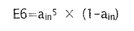
Furthermore, the heat-absorption coefficients V1, V2, V3, V4, V5, and V6 are represented as follows (likewise in the first embodiment). -


Furthermore, the heat-absorption coefficients V6', V5', V4', V3', V2', and V1' are represented as follows using the reflectivity b of the wafer. -


Thus, in this embodiment, not only the values of the reflectivity ain of the mirrors for in-band light and the values of the reflectivity aout of the mirrors for out-band light but also the value of the reflectivity b of thewafer 7 for out-band light affect the heat-absorption amount equation (10). Consequently, according to this embodiment, fluctuations in the image-forming characteristics can be controlled more accurately. - Note that, the value of the reflectivity b of the
wafer 7 is assumed to be temporally unchanged, but may vary according to the kind of thewafer 7. For this reason, it is desirable that thecontrolling part 9 have the value of "b" in the equations as a variable (parameter). Thus, it is desirable that the projection exposure apparatus of this embodiment have, for example, a user interface function allowing a user to input the value of the reflectivity b. Instead of this function, a sensor actually measuring the reflectivity b from thewafer 7 may be provided. The sensor consists of, for example, a light-emitting part emitting out-band light to part of thewafer 7, and a light-receiving part detecting the light quantity of the reflected light. In addition, if an average value (e.g. 0.7) of the reflectivity b is stored as a default value in thecontrolling part 9 in advance, it is also possible to save labor of the user input or the actual measurement. - Furthermore, this embodiment is a variation of the first embodiment, and the second embodiment or the third embodiment may also be similarly varied.
Claims (16)
- An exposure apparatus exposing an object to be exposed with light emitted from a light source, said exposure apparatus comprising a detecting unit detecting light quantity of non-exposure wavelength component of said light.
- The exposure apparatus according to claim 1, wherein said detecting unit detects light quantity of exposure wavelength component of said light and light quantity of non-exposure wavelength component of said light independently.
- The exposure apparatus according to claim 1 or 2, comprising:a projection optical system arranged between said light source and said object to be exposed; andan adjusting unit adjusting said projection optical system based on an output of said detecting unit.
- The exposure apparatus according to claim 3, wherein:said projection optical system includes at least one mirror; andat least one of subjects to be adjusted by said adjusting unit is a position of said mirror in a direction perpendicular to an optical axis.
- The exposure apparatus according to claim 3 or 4, wherein:said projection optical system includes at least one mirror; andat least one of the subjects to be adjusted by said adjusting unit is an attitude of said mirror.
- The exposure apparatus according to any one of claims 3 to 5, wherein:said projection optical system projects a pattern of a mask arranged on said light source's side onto said object to be exposed; andat least one of the subjects to be adjusted by said adjusting unit is a relative position between said mask and said object to be exposed.
- The exposure apparatus according to any one of claims 3 to 6, wherein:said projection optical system projects a pattern of a mask arranged on said light source's side onto said object to be exposed; andat least one of the subjects to be adjusted by said adjusting unit is an attitude of at least one of said mask and said object to be exposed.
- The exposure apparatus according to any one of claims 3 to 7, wherein:said detecting unit detects light quantity of exposure wavelength component of said light and light quantity of non-exposure wavelength component of said light independently; andsaid adjusting unit determines, to carry out said adjusting, adjustment contents of said projection optical system based on light quantity of said exposure wavelength component, light quantity of said non-exposure wavelength component, characteristic information of said projection optical system for said exposure wavelength component, and characteristic information of said projection optical system for said non-exposure wavelength component.
- The exposure apparatus according to claim 8: wherein,
said detecting unit includes at least two of the detecting units, which are a first detecting unit whose detecting object is light before passing said projection optical system, and a second detecting unit whose detecting object is light after passing said projection optical system; and wherein
said adjusting unit:corrects characteristic information of said projection optical system for said exposure wavelength component based on light quantity of said exposure wavelength component detected by said first detecting unit and light quantity of said exposure wavelength component detected by said second detecting unit; andcorrects characteristic information of said projection optical system for said non-exposure wavelength component based on light quantity of said non-exposure wavelength component detected by said first detecting unit and light quantity of said non-exposure wavelength component detected by said second detecting unit. - The exposure apparatus according to claim 8 or 9, wherein characteristic information of said projection optical system includes each of absorption coefficients of optical members in said projection optical system.
- The exposure apparatus according to any one of claims 8 to 10, wherein said adjusting unit reflects information about reflectivity of said object to be exposed for said non-exposure wavelength component in said adjustment contents.
- The exposure apparatus according to claim 11, further comprising a detecting unit detecting reflectivity of said object to be exposed for said non-exposure wavelength component.
- The exposure apparatus according to any one of claims 1 to 12, wherein said detecting unit comprises:a sensor for exposure wavelength detecting light quantity of exposure wavelength component of said light; anda sensor for non-exposure wavelength detecting light quantity of non-exposure wavelength component of said light.
- The exposure apparatus according to any one of claims 1 to 12, wherein said detecting unit includes:a sensor for specific wavelength detecting one of light quantity of exposure wavelength component and light quantity of non-exposure wavelength component of said light; anda sensor for all wavelengths detecting light quantity of all wavelength components of said light.
- The exposure apparatus according to any one of claims 1 to 12, wherein said detecting unit includes:a sensor for all wavelengths capable of detecting light quantity of all wavelength components of said light; anda switching unit switching wavelength of an incident light on said sensor for all wavelenghts between at least two of exposure wavelength, non-exposure wavelength, and all wavelengths.
- The exposure apparatus according to any one of claims 1 to 15, wherein said light source is an EUV light source.
Applications Claiming Priority (2)
| Application Number | Priority Date | Filing Date | Title |
|---|---|---|---|
| JP2005197031 | 2005-07-06 | ||
| PCT/JP2006/309657 WO2007004358A1 (en) | 2005-07-06 | 2006-05-15 | Exposure apparatus |
Publications (3)
| Publication Number | Publication Date |
|---|---|
| EP1901336A1 true EP1901336A1 (en) | 2008-03-19 |
| EP1901336A4 EP1901336A4 (en) | 2010-06-02 |
| EP1901336B1 EP1901336B1 (en) | 2012-01-11 |
Family
ID=37604234
Family Applications (1)
| Application Number | Title | Priority Date | Filing Date |
|---|---|---|---|
| EP06732588A Expired - Lifetime EP1901336B1 (en) | 2005-07-06 | 2006-05-15 | Exposure apparatus |
Country Status (6)
| Country | Link |
|---|---|
| EP (1) | EP1901336B1 (en) |
| JP (1) | JP4992714B2 (en) |
| KR (1) | KR101312854B1 (en) |
| CN (1) | CN100583394C (en) |
| TW (1) | TWI411894B (en) |
| WO (1) | WO2007004358A1 (en) |
Cited By (1)
| Publication number | Priority date | Publication date | Assignee | Title |
|---|---|---|---|---|
| WO2015161948A1 (en) * | 2014-04-25 | 2015-10-29 | Asml Netherlands B.V. | Lithographic apparatus and device manufacturing method |
Families Citing this family (7)
| Publication number | Priority date | Publication date | Assignee | Title |
|---|---|---|---|---|
| JP2008124065A (en) * | 2006-11-08 | 2008-05-29 | Nikon Corp | Exposure apparatus and device manufacturing method |
| US7829249B2 (en) | 2007-03-05 | 2010-11-09 | Asml Netherlands B.V. | Device manufacturing method, computer program and lithographic apparatus |
| JP4986754B2 (en) * | 2007-07-27 | 2012-07-25 | キヤノン株式会社 | Illumination optical system and exposure apparatus having the same |
| WO2010032753A1 (en) | 2008-09-18 | 2010-03-25 | 株式会社ニコン | Aperture stop, optical system, exposure apparatus and electronic device manufacturing method |
| KR101616047B1 (en) * | 2009-02-09 | 2016-04-28 | 삼성전자주식회사 | A Reflectance Measurement System of EUV Photolithography Apparatus |
| US9075322B2 (en) * | 2010-09-10 | 2015-07-07 | Nikon Corporation | Reflective imaging optical system, exposure apparatus, and method for producing device |
| KR101359754B1 (en) * | 2012-06-22 | 2014-02-10 | 주식회사 에프에스티 | Precision adjustable optical EUV light generating device |
Family Cites Families (12)
| Publication number | Priority date | Publication date | Assignee | Title |
|---|---|---|---|---|
| JPH0936018A (en) | 1995-07-20 | 1997-02-07 | Nikon Corp | Projection exposure device |
| JP3661291B2 (en) * | 1996-08-01 | 2005-06-15 | 株式会社ニコン | Exposure equipment |
| JP2000100697A (en) * | 1998-09-22 | 2000-04-07 | Nikon Corp | Exposure apparatus adjustment method and exposure apparatus |
| US6727980B2 (en) * | 1998-09-17 | 2004-04-27 | Nikon Corporation | Apparatus and method for pattern exposure and method for adjusting the apparatus |
| JP2000131439A (en) * | 1998-10-29 | 2000-05-12 | Hitachi Ltd | X-ray intensity monitor and X-ray utilization apparatus using the X-ray intensity monitor |
| JP3091460B1 (en) * | 1999-12-10 | 2000-09-25 | 東レエンジニアリング株式会社 | Exposure equipment |
| JP4803901B2 (en) * | 2001-05-22 | 2011-10-26 | キヤノン株式会社 | Alignment method, exposure apparatus, and semiconductor device manufacturing method |
| JP2002353099A (en) * | 2001-05-22 | 2002-12-06 | Canon Inc | Position detecting method and apparatus, exposure apparatus and device manufacturing method |
| KR100566152B1 (en) * | 2002-08-30 | 2006-03-31 | 에이에스엠엘 네델란즈 비.브이. | Lithographic Apparatus and Device Manufacturing Method |
| JP4113418B2 (en) * | 2002-11-15 | 2008-07-09 | 富士フイルム株式会社 | Exposure equipment |
| JP4262032B2 (en) * | 2003-08-25 | 2009-05-13 | キヤノン株式会社 | EUV light source spectrum measurement device |
| US7369216B2 (en) * | 2004-10-15 | 2008-05-06 | Asml Netherlands B.V. | Lithographic system, method for adapting transmission characteristics of an optical pathway within a lithographic system, semiconductor device, method of manufacturing a reflective element for use in a lithographic system, and reflective element manufactured thereby |
-
2006
- 2006-05-15 EP EP06732588A patent/EP1901336B1/en not_active Expired - Lifetime
- 2006-05-15 WO PCT/JP2006/309657 patent/WO2007004358A1/en not_active Ceased
- 2006-05-15 JP JP2007523357A patent/JP4992714B2/en not_active Expired - Fee Related
- 2006-05-15 KR KR1020077027316A patent/KR101312854B1/en not_active Expired - Fee Related
- 2006-05-15 CN CN200680013662A patent/CN100583394C/en not_active Expired - Fee Related
- 2006-05-22 TW TW095118061A patent/TWI411894B/en not_active IP Right Cessation
Cited By (1)
| Publication number | Priority date | Publication date | Assignee | Title |
|---|---|---|---|---|
| WO2015161948A1 (en) * | 2014-04-25 | 2015-10-29 | Asml Netherlands B.V. | Lithographic apparatus and device manufacturing method |
Also Published As
| Publication number | Publication date |
|---|---|
| JP4992714B2 (en) | 2012-08-08 |
| KR101312854B1 (en) | 2013-09-30 |
| TWI411894B (en) | 2013-10-11 |
| JPWO2007004358A1 (en) | 2009-01-22 |
| WO2007004358A1 (en) | 2007-01-11 |
| TW200702950A (en) | 2007-01-16 |
| CN100583394C (en) | 2010-01-20 |
| CN101164146A (en) | 2008-04-16 |
| EP1901336A4 (en) | 2010-06-02 |
| EP1901336B1 (en) | 2012-01-11 |
| KR20080016814A (en) | 2008-02-22 |
Similar Documents
| Publication | Publication Date | Title |
|---|---|---|
| US7965387B2 (en) | Image plane measurement method, exposure method, device manufacturing method, and exposure apparatus | |
| WO2007004567A1 (en) | Exposure apparatus, exposure method, device manufacturing method, and system | |
| KR100200384B1 (en) | Projection exposure apparatus and device manufacturing method using the same | |
| US7941232B2 (en) | Control method, control system, and program | |
| US7760326B2 (en) | Exposure apparatus and aberration correction method | |
| WO1998059364A1 (en) | Projection aligner, method of manufacturing the aligner, method of exposure using the aligner, and method of manufacturing circuit devices by using the aligner | |
| JPH06291016A (en) | Projection exposure device | |
| EP1901336B1 (en) | Exposure apparatus | |
| US20130342819A1 (en) | Exposure apparatus, exposure method, and method of manufacturing article | |
| WO2002043123A1 (en) | Aligner, aligning method and method for fabricating device | |
| US6492649B1 (en) | Projection exposure apparatus, projection exposure method, optical cleaning method and method of fabricating semiconductor device | |
| JP3473649B2 (en) | Projection exposure equipment | |
| US7812928B2 (en) | Exposure apparatus | |
| US20180074278A1 (en) | Method for producing a lens for a lithography apparatus, and measurement system | |
| EP1335460B1 (en) | Laser apparatus, exposure apparatus and method | |
| US20090231562A1 (en) | Effective light source shape database generation method, optical image calculation method, recording medium, exposure method, and device fabrication method | |
| JP3414476B2 (en) | Projection exposure equipment | |
| US7369216B2 (en) | Lithographic system, method for adapting transmission characteristics of an optical pathway within a lithographic system, semiconductor device, method of manufacturing a reflective element for use in a lithographic system, and reflective element manufactured thereby | |
| JPWO2002025710A1 (en) | Exposure apparatus, exposure method, and device manufacturing method | |
| JP2012234883A (en) | Exposure apparatus, exposure method, and method for manufacturing device | |
| KR100588127B1 (en) | Lithographic Apparatus, Method of Manufacturing a Device, and Device Manufactured Thereby | |
| JP2590891B2 (en) | Projection optical device | |
| JPH11154644A (en) | Projection exposure equipment | |
| JP2705694B2 (en) | Projection optical device | |
| JP3245026B2 (en) | Exposure method, exposure apparatus, and device manufacturing method using the same |
Legal Events
| Date | Code | Title | Description |
|---|---|---|---|
| PUAI | Public reference made under article 153(3) epc to a published international application that has entered the european phase |
Free format text: ORIGINAL CODE: 0009012 |
|
| 17P | Request for examination filed |
Effective date: 20071212 |
|
| AK | Designated contracting states |
Kind code of ref document: A1 Designated state(s): AT BE BG CH CY CZ DE DK EE ES FI FR GB GR HU IE IS IT LI LT LU LV MC NL PL PT RO SE SI SK TR |
|
| RIN1 | Information on inventor provided before grant (corrected) |
Inventor name: SHIRAISHI MASAYUKI |
|
| A4 | Supplementary search report drawn up and despatched |
Effective date: 20100504 |
|
| RAP1 | Party data changed (applicant data changed or rights of an application transferred) |
Owner name: NIKON CORPORATION |
|
| RIN1 | Information on inventor provided before grant (corrected) |
Inventor name: SHIRAISHI MASAYUKI |
|
| GRAP | Despatch of communication of intention to grant a patent |
Free format text: ORIGINAL CODE: EPIDOSNIGR1 |
|
| RIC1 | Information provided on ipc code assigned before grant |
Ipc: H01L 21/027 20060101AFI20110609BHEP Ipc: G03F 7/20 20060101ALI20110609BHEP |
|
| DAX | Request for extension of the european patent (deleted) | ||
| GRAS | Grant fee paid |
Free format text: ORIGINAL CODE: EPIDOSNIGR3 |
|
| GRAA | (expected) grant |
Free format text: ORIGINAL CODE: 0009210 |
|
| AK | Designated contracting states |
Kind code of ref document: B1 Designated state(s): AT BE BG CH CY CZ DE DK EE ES FI FR GB GR HU IE IS IT LI LT LU LV MC NL PL PT RO SE SI SK TR |
|
| REG | Reference to a national code |
Ref country code: GB Ref legal event code: FG4D |
|
| REG | Reference to a national code |
Ref country code: CH Ref legal event code: EP |
|
| REG | Reference to a national code |
Ref country code: AT Ref legal event code: REF Ref document number: 541304 Country of ref document: AT Kind code of ref document: T Effective date: 20120115 |
|
| REG | Reference to a national code |
Ref country code: IE Ref legal event code: FG4D |
|
| REG | Reference to a national code |
Ref country code: NL Ref legal event code: T3 |
|
| REG | Reference to a national code |
Ref country code: DE Ref legal event code: R096 Ref document number: 602006027007 Country of ref document: DE Effective date: 20120308 |
|
| PG25 | Lapsed in a contracting state [announced via postgrant information from national office to epo] |
Ref country code: SI Free format text: LAPSE BECAUSE OF FAILURE TO SUBMIT A TRANSLATION OF THE DESCRIPTION OR TO PAY THE FEE WITHIN THE PRESCRIBED TIME-LIMIT Effective date: 20120111 |
|
| LTIE | Lt: invalidation of european patent or patent extension |
Effective date: 20120111 |
|
| PG25 | Lapsed in a contracting state [announced via postgrant information from national office to epo] |
Ref country code: IS Free format text: LAPSE BECAUSE OF FAILURE TO SUBMIT A TRANSLATION OF THE DESCRIPTION OR TO PAY THE FEE WITHIN THE PRESCRIBED TIME-LIMIT Effective date: 20120511 Ref country code: BE Free format text: LAPSE BECAUSE OF FAILURE TO SUBMIT A TRANSLATION OF THE DESCRIPTION OR TO PAY THE FEE WITHIN THE PRESCRIBED TIME-LIMIT Effective date: 20120111 Ref country code: LT Free format text: LAPSE BECAUSE OF FAILURE TO SUBMIT A TRANSLATION OF THE DESCRIPTION OR TO PAY THE FEE WITHIN THE PRESCRIBED TIME-LIMIT Effective date: 20120111 Ref country code: BG Free format text: LAPSE BECAUSE OF FAILURE TO SUBMIT A TRANSLATION OF THE DESCRIPTION OR TO PAY THE FEE WITHIN THE PRESCRIBED TIME-LIMIT Effective date: 20120411 |
|
| PG25 | Lapsed in a contracting state [announced via postgrant information from national office to epo] |
Ref country code: FI Free format text: LAPSE BECAUSE OF FAILURE TO SUBMIT A TRANSLATION OF THE DESCRIPTION OR TO PAY THE FEE WITHIN THE PRESCRIBED TIME-LIMIT Effective date: 20120111 Ref country code: PL Free format text: LAPSE BECAUSE OF FAILURE TO SUBMIT A TRANSLATION OF THE DESCRIPTION OR TO PAY THE FEE WITHIN THE PRESCRIBED TIME-LIMIT Effective date: 20120111 Ref country code: PT Free format text: LAPSE BECAUSE OF FAILURE TO SUBMIT A TRANSLATION OF THE DESCRIPTION OR TO PAY THE FEE WITHIN THE PRESCRIBED TIME-LIMIT Effective date: 20120511 Ref country code: GR Free format text: LAPSE BECAUSE OF FAILURE TO SUBMIT A TRANSLATION OF THE DESCRIPTION OR TO PAY THE FEE WITHIN THE PRESCRIBED TIME-LIMIT Effective date: 20120412 Ref country code: LV Free format text: LAPSE BECAUSE OF FAILURE TO SUBMIT A TRANSLATION OF THE DESCRIPTION OR TO PAY THE FEE WITHIN THE PRESCRIBED TIME-LIMIT Effective date: 20120111 |
|
| REG | Reference to a national code |
Ref country code: AT Ref legal event code: MK05 Ref document number: 541304 Country of ref document: AT Kind code of ref document: T Effective date: 20120111 |
|
| PG25 | Lapsed in a contracting state [announced via postgrant information from national office to epo] |
Ref country code: CY Free format text: LAPSE BECAUSE OF FAILURE TO SUBMIT A TRANSLATION OF THE DESCRIPTION OR TO PAY THE FEE WITHIN THE PRESCRIBED TIME-LIMIT Effective date: 20120111 |
|
| PG25 | Lapsed in a contracting state [announced via postgrant information from national office to epo] |
Ref country code: RO Free format text: LAPSE BECAUSE OF FAILURE TO SUBMIT A TRANSLATION OF THE DESCRIPTION OR TO PAY THE FEE WITHIN THE PRESCRIBED TIME-LIMIT Effective date: 20120111 Ref country code: SE Free format text: LAPSE BECAUSE OF FAILURE TO SUBMIT A TRANSLATION OF THE DESCRIPTION OR TO PAY THE FEE WITHIN THE PRESCRIBED TIME-LIMIT Effective date: 20120111 Ref country code: CZ Free format text: LAPSE BECAUSE OF FAILURE TO SUBMIT A TRANSLATION OF THE DESCRIPTION OR TO PAY THE FEE WITHIN THE PRESCRIBED TIME-LIMIT Effective date: 20120111 Ref country code: EE Free format text: LAPSE BECAUSE OF FAILURE TO SUBMIT A TRANSLATION OF THE DESCRIPTION OR TO PAY THE FEE WITHIN THE PRESCRIBED TIME-LIMIT Effective date: 20120111 Ref country code: DK Free format text: LAPSE BECAUSE OF FAILURE TO SUBMIT A TRANSLATION OF THE DESCRIPTION OR TO PAY THE FEE WITHIN THE PRESCRIBED TIME-LIMIT Effective date: 20120111 |
|
| PLBE | No opposition filed within time limit |
Free format text: ORIGINAL CODE: 0009261 |
|
| STAA | Information on the status of an ep patent application or granted ep patent |
Free format text: STATUS: NO OPPOSITION FILED WITHIN TIME LIMIT |
|
| PG25 | Lapsed in a contracting state [announced via postgrant information from national office to epo] |
Ref country code: SK Free format text: LAPSE BECAUSE OF FAILURE TO SUBMIT A TRANSLATION OF THE DESCRIPTION OR TO PAY THE FEE WITHIN THE PRESCRIBED TIME-LIMIT Effective date: 20120111 Ref country code: IT Free format text: LAPSE BECAUSE OF FAILURE TO SUBMIT A TRANSLATION OF THE DESCRIPTION OR TO PAY THE FEE WITHIN THE PRESCRIBED TIME-LIMIT Effective date: 20120111 |
|
| 26N | No opposition filed |
Effective date: 20121012 |
|
| PG25 | Lapsed in a contracting state [announced via postgrant information from national office to epo] |
Ref country code: MC Free format text: LAPSE BECAUSE OF NON-PAYMENT OF DUE FEES Effective date: 20120531 |
|
| REG | Reference to a national code |
Ref country code: CH Ref legal event code: PL |
|
| GBPC | Gb: european patent ceased through non-payment of renewal fee |
Effective date: 20120515 |
|
| PG25 | Lapsed in a contracting state [announced via postgrant information from national office to epo] |
Ref country code: LI Free format text: LAPSE BECAUSE OF NON-PAYMENT OF DUE FEES Effective date: 20120531 Ref country code: AT Free format text: LAPSE BECAUSE OF FAILURE TO SUBMIT A TRANSLATION OF THE DESCRIPTION OR TO PAY THE FEE WITHIN THE PRESCRIBED TIME-LIMIT Effective date: 20120111 Ref country code: CH Free format text: LAPSE BECAUSE OF NON-PAYMENT OF DUE FEES Effective date: 20120531 |
|
| REG | Reference to a national code |
Ref country code: DE Ref legal event code: R097 Ref document number: 602006027007 Country of ref document: DE Effective date: 20121012 |
|
| REG | Reference to a national code |
Ref country code: IE Ref legal event code: MM4A |
|
| REG | Reference to a national code |
Ref country code: FR Ref legal event code: ST Effective date: 20130131 |
|
| PG25 | Lapsed in a contracting state [announced via postgrant information from national office to epo] |
Ref country code: GB Free format text: LAPSE BECAUSE OF NON-PAYMENT OF DUE FEES Effective date: 20120515 Ref country code: FR Free format text: LAPSE BECAUSE OF NON-PAYMENT OF DUE FEES Effective date: 20120531 Ref country code: IE Free format text: LAPSE BECAUSE OF NON-PAYMENT OF DUE FEES Effective date: 20120515 Ref country code: ES Free format text: LAPSE BECAUSE OF FAILURE TO SUBMIT A TRANSLATION OF THE DESCRIPTION OR TO PAY THE FEE WITHIN THE PRESCRIBED TIME-LIMIT Effective date: 20120422 |
|
| PG25 | Lapsed in a contracting state [announced via postgrant information from national office to epo] |
Ref country code: TR Free format text: LAPSE BECAUSE OF FAILURE TO SUBMIT A TRANSLATION OF THE DESCRIPTION OR TO PAY THE FEE WITHIN THE PRESCRIBED TIME-LIMIT Effective date: 20120111 |
|
| PG25 | Lapsed in a contracting state [announced via postgrant information from national office to epo] |
Ref country code: LU Free format text: LAPSE BECAUSE OF NON-PAYMENT OF DUE FEES Effective date: 20120515 |
|
| PG25 | Lapsed in a contracting state [announced via postgrant information from national office to epo] |
Ref country code: HU Free format text: LAPSE BECAUSE OF FAILURE TO SUBMIT A TRANSLATION OF THE DESCRIPTION OR TO PAY THE FEE WITHIN THE PRESCRIBED TIME-LIMIT Effective date: 20060515 |
|
| PGFP | Annual fee paid to national office [announced via postgrant information from national office to epo] |
Ref country code: NL Payment date: 20220420 Year of fee payment: 17 |
|
| PGFP | Annual fee paid to national office [announced via postgrant information from national office to epo] |
Ref country code: DE Payment date: 20220329 Year of fee payment: 17 |
|
| REG | Reference to a national code |
Ref country code: DE Ref legal event code: R119 Ref document number: 602006027007 Country of ref document: DE |
|
| REG | Reference to a national code |
Ref country code: NL Ref legal event code: MM Effective date: 20230601 |
|
| PG25 | Lapsed in a contracting state [announced via postgrant information from national office to epo] |
Ref country code: NL Free format text: LAPSE BECAUSE OF NON-PAYMENT OF DUE FEES Effective date: 20230601 |
|
| PG25 | Lapsed in a contracting state [announced via postgrant information from national office to epo] |
Ref country code: DE Free format text: LAPSE BECAUSE OF NON-PAYMENT OF DUE FEES Effective date: 20231201 |