EP1895821A1 - Printed wiring board with component-mounting pins and electronic equipment using the same - Google Patents
Printed wiring board with component-mounting pins and electronic equipment using the same Download PDFInfo
- Publication number
- EP1895821A1 EP1895821A1 EP06833716A EP06833716A EP1895821A1 EP 1895821 A1 EP1895821 A1 EP 1895821A1 EP 06833716 A EP06833716 A EP 06833716A EP 06833716 A EP06833716 A EP 06833716A EP 1895821 A1 EP1895821 A1 EP 1895821A1
- Authority
- EP
- European Patent Office
- Prior art keywords
- printed wiring
- wiring board
- component mounting
- mounting pin
- layer
- Prior art date
- Legal status (The legal status is an assumption and is not a legal conclusion. Google has not performed a legal analysis and makes no representation as to the accuracy of the status listed.)
- Ceased
Links
Images



Classifications
-
- H—ELECTRICITY
- H05—ELECTRIC TECHNIQUES NOT OTHERWISE PROVIDED FOR
- H05K—PRINTED CIRCUITS; CASINGS OR CONSTRUCTIONAL DETAILS OF ELECTRIC APPARATUS; MANUFACTURE OF ASSEMBLAGES OF ELECTRICAL COMPONENTS
- H05K1/00—Printed circuits
- H05K1/02—Details
-
- H—ELECTRICITY
- H05—ELECTRIC TECHNIQUES NOT OTHERWISE PROVIDED FOR
- H05K—PRINTED CIRCUITS; CASINGS OR CONSTRUCTIONAL DETAILS OF ELECTRIC APPARATUS; MANUFACTURE OF ASSEMBLAGES OF ELECTRICAL COMPONENTS
- H05K3/00—Apparatus or processes for manufacturing printed circuits
- H05K3/30—Assembling printed circuits with electric components, e.g. with resistors
- H05K3/32—Assembling printed circuits with electric components, e.g. with resistors electrically connecting electric components or wires to printed circuits
- H05K3/325—Assembling printed circuits with electric components, e.g. with resistors electrically connecting electric components or wires to printed circuits by abutting or pinching; Mechanical auxiliary parts therefor
- H05K3/326—Assembling printed circuits with electric components, e.g. with resistors electrically connecting electric components or wires to printed circuits by abutting or pinching; Mechanical auxiliary parts therefor the printed circuit having integral resilient or deformable parts, e.g. tabs or parts of flexible circuits
-
- H—ELECTRICITY
- H05—ELECTRIC TECHNIQUES NOT OTHERWISE PROVIDED FOR
- H05K—PRINTED CIRCUITS; CASINGS OR CONSTRUCTIONAL DETAILS OF ELECTRIC APPARATUS; MANUFACTURE OF ASSEMBLAGES OF ELECTRICAL COMPONENTS
- H05K1/00—Printed circuits
- H05K1/18—Printed circuits structurally associated with non-printed electric components
-
- H—ELECTRICITY
- H05—ELECTRIC TECHNIQUES NOT OTHERWISE PROVIDED FOR
- H05K—PRINTED CIRCUITS; CASINGS OR CONSTRUCTIONAL DETAILS OF ELECTRIC APPARATUS; MANUFACTURE OF ASSEMBLAGES OF ELECTRICAL COMPONENTS
- H05K3/00—Apparatus or processes for manufacturing printed circuits
- H05K3/30—Assembling printed circuits with electric components, e.g. with resistors
-
- H—ELECTRICITY
- H05—ELECTRIC TECHNIQUES NOT OTHERWISE PROVIDED FOR
- H05K—PRINTED CIRCUITS; CASINGS OR CONSTRUCTIONAL DETAILS OF ELECTRIC APPARATUS; MANUFACTURE OF ASSEMBLAGES OF ELECTRICAL COMPONENTS
- H05K3/00—Apparatus or processes for manufacturing printed circuits
- H05K3/40—Forming printed elements for providing electric connections to or between printed circuits
- H05K3/4092—Integral conductive tabs, i.e. conductive parts partly detached from the substrate
-
- H—ELECTRICITY
- H10—SEMICONDUCTOR DEVICES; ELECTRIC SOLID-STATE DEVICES NOT OTHERWISE PROVIDED FOR
- H10W—GENERIC PACKAGES, INTERCONNECTIONS, CONNECTORS OR OTHER CONSTRUCTIONAL DETAILS OF DEVICES COVERED BY CLASS H10
- H10W72/00—Interconnections or connectors in packages
-
- H—ELECTRICITY
- H10—SEMICONDUCTOR DEVICES; ELECTRIC SOLID-STATE DEVICES NOT OTHERWISE PROVIDED FOR
- H10W—GENERIC PACKAGES, INTERCONNECTIONS, CONNECTORS OR OTHER CONSTRUCTIONAL DETAILS OF DEVICES COVERED BY CLASS H10
- H10W90/00—Package configurations
- H10W90/701—Package configurations characterised by the relative positions of pads or connectors relative to package parts
-
- H—ELECTRICITY
- H05—ELECTRIC TECHNIQUES NOT OTHERWISE PROVIDED FOR
- H05K—PRINTED CIRCUITS; CASINGS OR CONSTRUCTIONAL DETAILS OF ELECTRIC APPARATUS; MANUFACTURE OF ASSEMBLAGES OF ELECTRICAL COMPONENTS
- H05K2201/00—Indexing scheme relating to printed circuits covered by H05K1/00
- H05K2201/03—Conductive materials
- H05K2201/0302—Properties and characteristics in general
- H05K2201/0311—Metallic part with specific elastic properties, e.g. bent piece of metal as electrical contact
-
- H—ELECTRICITY
- H05—ELECTRIC TECHNIQUES NOT OTHERWISE PROVIDED FOR
- H05K—PRINTED CIRCUITS; CASINGS OR CONSTRUCTIONAL DETAILS OF ELECTRIC APPARATUS; MANUFACTURE OF ASSEMBLAGES OF ELECTRICAL COMPONENTS
- H05K2201/00—Indexing scheme relating to printed circuits covered by H05K1/00
- H05K2201/03—Conductive materials
- H05K2201/0302—Properties and characteristics in general
- H05K2201/0314—Elastomeric connector or conductor, e.g. rubber with metallic filler
-
- H—ELECTRICITY
- H05—ELECTRIC TECHNIQUES NOT OTHERWISE PROVIDED FOR
- H05K—PRINTED CIRCUITS; CASINGS OR CONSTRUCTIONAL DETAILS OF ELECTRIC APPARATUS; MANUFACTURE OF ASSEMBLAGES OF ELECTRICAL COMPONENTS
- H05K2201/00—Indexing scheme relating to printed circuits covered by H05K1/00
- H05K2201/03—Conductive materials
- H05K2201/0332—Structure of the conductor
- H05K2201/0388—Other aspects of conductors
- H05K2201/0397—Tab
-
- H—ELECTRICITY
- H05—ELECTRIC TECHNIQUES NOT OTHERWISE PROVIDED FOR
- H05K—PRINTED CIRCUITS; CASINGS OR CONSTRUCTIONAL DETAILS OF ELECTRIC APPARATUS; MANUFACTURE OF ASSEMBLAGES OF ELECTRICAL COMPONENTS
- H05K3/00—Apparatus or processes for manufacturing printed circuits
- H05K3/22—Secondary treatment of printed circuits
- H05K3/28—Applying non-metallic protective coatings
-
- H—ELECTRICITY
- H05—ELECTRIC TECHNIQUES NOT OTHERWISE PROVIDED FOR
- H05K—PRINTED CIRCUITS; CASINGS OR CONSTRUCTIONAL DETAILS OF ELECTRIC APPARATUS; MANUFACTURE OF ASSEMBLAGES OF ELECTRICAL COMPONENTS
- H05K3/00—Apparatus or processes for manufacturing printed circuits
- H05K3/30—Assembling printed circuits with electric components, e.g. with resistors
- H05K3/32—Assembling printed circuits with electric components, e.g. with resistors electrically connecting electric components or wires to printed circuits
- H05K3/34—Assembling printed circuits with electric components, e.g. with resistors electrically connecting electric components or wires to printed circuits by soldering
- H05K3/341—Surface mounted components
-
- H—ELECTRICITY
- H10—SEMICONDUCTOR DEVICES; ELECTRIC SOLID-STATE DEVICES NOT OTHERWISE PROVIDED FOR
- H10W—GENERIC PACKAGES, INTERCONNECTIONS, CONNECTORS OR OTHER CONSTRUCTIONAL DETAILS OF DEVICES COVERED BY CLASS H10
- H10W72/00—Interconnections or connectors in packages
- H10W72/01—Manufacture or treatment
- H10W72/012—Manufacture or treatment of bump connectors, dummy bumps or thermal bumps
- H10W72/01221—Manufacture or treatment of bump connectors, dummy bumps or thermal bumps using local deposition
- H10W72/01225—Manufacture or treatment of bump connectors, dummy bumps or thermal bumps using local deposition in solid form, e.g. by using a powder or by stud bumping
-
- H—ELECTRICITY
- H10—SEMICONDUCTOR DEVICES; ELECTRIC SOLID-STATE DEVICES NOT OTHERWISE PROVIDED FOR
- H10W—GENERIC PACKAGES, INTERCONNECTIONS, CONNECTORS OR OTHER CONSTRUCTIONAL DETAILS OF DEVICES COVERED BY CLASS H10
- H10W72/00—Interconnections or connectors in packages
- H10W72/071—Connecting or disconnecting
- H10W72/072—Connecting or disconnecting of bump connectors
- H10W72/07231—Techniques
- H10W72/07234—Using a reflow oven
-
- H—ELECTRICITY
- H10—SEMICONDUCTOR DEVICES; ELECTRIC SOLID-STATE DEVICES NOT OTHERWISE PROVIDED FOR
- H10W—GENERIC PACKAGES, INTERCONNECTIONS, CONNECTORS OR OTHER CONSTRUCTIONAL DETAILS OF DEVICES COVERED BY CLASS H10
- H10W72/00—Interconnections or connectors in packages
- H10W72/071—Connecting or disconnecting
- H10W72/072—Connecting or disconnecting of bump connectors
- H10W72/07231—Techniques
- H10W72/07236—Soldering or alloying
-
- H—ELECTRICITY
- H10—SEMICONDUCTOR DEVICES; ELECTRIC SOLID-STATE DEVICES NOT OTHERWISE PROVIDED FOR
- H10W—GENERIC PACKAGES, INTERCONNECTIONS, CONNECTORS OR OTHER CONSTRUCTIONAL DETAILS OF DEVICES COVERED BY CLASS H10
- H10W72/00—Interconnections or connectors in packages
- H10W72/20—Bump connectors, e.g. solder bumps or copper pillars; Dummy bumps; Thermal bumps
- H10W72/251—Materials
- H10W72/252—Materials comprising solid metals or solid metalloids, e.g. PbSn, Ag or Cu
-
- H—ELECTRICITY
- H10—SEMICONDUCTOR DEVICES; ELECTRIC SOLID-STATE DEVICES NOT OTHERWISE PROVIDED FOR
- H10W—GENERIC PACKAGES, INTERCONNECTIONS, CONNECTORS OR OTHER CONSTRUCTIONAL DETAILS OF DEVICES COVERED BY CLASS H10
- H10W72/00—Interconnections or connectors in packages
- H10W72/90—Bond pads, in general
-
- H—ELECTRICITY
- H10—SEMICONDUCTOR DEVICES; ELECTRIC SOLID-STATE DEVICES NOT OTHERWISE PROVIDED FOR
- H10W—GENERIC PACKAGES, INTERCONNECTIONS, CONNECTORS OR OTHER CONSTRUCTIONAL DETAILS OF DEVICES COVERED BY CLASS H10
- H10W72/00—Interconnections or connectors in packages
- H10W72/90—Bond pads, in general
- H10W72/941—Dispositions of bond pads
- H10W72/9415—Dispositions of bond pads relative to the surface, e.g. recessed, protruding
Definitions
- the present invention relates to a printed wiring board with a component mounting pin and an electronic device using the same, and more particularly to a printed wiring board with a component mounting pin for use in mounting surface-mounting type parts and an electronic device using the same.
- a number of electronic components are employed to fabricate electronic apparatus.
- a printed wiring board is used to electrically connect electrode pads of these semiconductor apparatus. Since it is inevitable that highly-integrated semiconductor apparatus includes a large number of electrodes, in order to mount such semiconductor apparatus on a printed wiring board with a limited area, it is customary that a flip-chip mounting system is used to mount the electrode pads of the semiconductor chip on the printed wiring board in such a manner that their surfaces are opposed to the printed wiring board to thereby connect the electrode pads to the lands of the printed wiring board mounting surface by a suitable technology such as solder bump.
- printed wiring board refers to a board with a wiring pattern formed on an insulating substrate
- printed circuit board refers to a component product in which electronic components such as IC and LSI are mounted on the printed wiring board.
- the printed circuit board is a component product of an electronic component with predetermined objects and therefore referred to as an "electronic device”.
- the Background Art of the Patent Document 1 has described a flip-chip mounting system printed circuit board using suitable technology such as solder bump in which a solder resist layer 70 is formed on an upper layer of a via hole 160 and a conductor circuit 158, bumps 76U and 76D being formed on the via hole 160 and the conductor circuit 158 through an opening portion 71 of the solder resist layer 70.
- An IC chip, not shown may be electrically connected to the printed circuit board by C4 (flip-chip) mounting.
- Patent Document 1 fails to mention a printed wiring board with a component mounting pin disclosed in the present application.
- the present invention intends to provide a printed wiring board in which malconnection or disconnection caused by a difference between the coefficients of thermal expansion of an electronic component and a printed wiring board can be decreased even when a highly-integrated electronic component is mounted thereon.
- the present invention intends to provide an electronic device in which malconnection or disconnection caused by a difference between the coefficients of thermal expansion of a semiconductor chip and a printed wiring board can be decreased even when a highly-integrated electronic component is mounted thereon.
- a printed wiring board of the present invention includes component mounting pin.
- said component mounting pin may be elongated from an outermost conductor of said printed wiring board and the other end thereof may be erected from said printed wiring board.
- said component mounting pin may be made of an elastic material.
- said component mounting pin may be made of a material with low electric resistance.
- said component mounting pin may be made of any material selected from a group consisting of a metal, a conductive rubber, a partly-conductive rubber, a conductive synthetic resin and a partly-conductive synthetic resin.
- stress of an n-1th layer may be tensile stress relative to stress of said nth layer or it is equal to the stress of said nth layer, and stress of said first layer may be tensile stress relative to the stress of said nth layer.
- said n-1th layer may have an equal or higher coefficient of thermal expansion to or than that of thermal expansion of said nth layer, and said first layer may have a higher coefficient of thermal expansion than that of thermal expansion of said nth layer.
- said component mounting pin may have a conductive protective coating formed thereon.
- said component mounting pin may have a solder bump formed at its tip end portion.
- an electronic device of the present invention comprises: a printed wiring board with a component mounting pin; and a surface-mounting type component with an electrode pad, wherein said component mounting pin is electrically connected to said electrode pad.
- said component mounting pin may have elasticity and may be urged against said electrode pad.
- said component mounting pin may be short in length.
- said component mounting pin may be elongated from an outermost conductor of said printed wiring board, erected upward and connected to said electrode pad and the portion in which said component mounting pin ma be erected upward is enclosed by the air.
- an electronic device of the present invention comprises: a printed wiring board with a component mounting pin; and a surface-mounting type component with an electrode pad, wherein said component mounting pin has a solder bump formed at its tip end portion and is soldered to said electrode pad.
- FIG. 1 of the accompanying drawings is a diagram showing part of a printed wiring board with a component mounting pin.
- a printed wiring board 1 according to the embodiment of the present invention includes a component mounting pin 18 to connect with an electronic component (not shown) like a semiconductor apparatus such as an IC and an LSI.
- the printed wiring board 1 with a component mounting pin is characterized by the component mounting pin 18 electrically connected to an outermost conductor 11. Accordingly, a rest of the arrangement of the printed wiring board 1 can be changed freely. Since the embodiment of the present invention is characterized by the outermost conductor, the printed wiring board 1 will be described such that an insulating layer 10 with the outermost layer conductor 11 formed thereon, a solder resist layer 12 formed on the insulating layer 10 and other layer 9 formed under the insulating layer 10, each of which comprises the printed wiring board 1, will be highlighted separately in order to understand the present embodiment more clearly.
- the printed wiring board 1 includes the solder resist layer 12 with an opening 12a and the substrates 9 and 10.
- the substrate 10 is the insulating layer formed under the solder resist layer 12 and the substrate 9 is composed of a predetermined conductive layer and an insulating layer.
- the insulating layer 10 has a filled via hole 5 and the upper portion of the filled via hole 5 is formed as the outermost conductor 11.
- One end of the component mounting pin 18 is electrically connected to the outermost conductor 11 and the other end thereof is erected upward from the printed wiring board 1.
- the component mounting pin 18 might be covered with a desired conductive protective coating 19 if necessary.
- the printed wiring board 1 is connected to a semiconductor apparatus (not shown) by this component mounting pin 18.
- the component mounting pin 18 is made of a material having suitable properties such as flexibility, elasticity and pliability and should preferably be made of a material with low electric resistance in addition to flexibility, elasticity and pliability.
- This elastic material for example, might be any material selected from a group consisting of metal, conductive rubber, partly-conductive rubber, conductive synthetic resin and partly-conductive synthetic resin.
- the component mounting pin 18 might be formed of films of n layers (n ⁇ 2 wherein a first layer is assumed to be disposed on the side opposing to the printed wiring board 1). If the film of the nth layer is easy to contract relative to the film of the first layer, the film of the nth layer need not contract relative to a film of an n-1th layer.
- the above film arrangement may be provided by suitable methods such as to cause the film of the nth layer to be under compressive stress relative to the film of the first layer and to cause the film of the nth layer to have a lower coefficient of thermal expansion than a coefficient of thermal expansion of the film of the first layer.
- the film of the n-1th layer may be under tensile stress relative to the film of the nth layer or the film of the n-th layer may be without tensile stress or compressive stress relative to the film of the nth layer.
- the film of the n-1th layer may have a higher coefficient of thermal expansion than a coefficient of thermal expansion of the film of the nth layer or the film of the n-th layer may have an equal coefficient of thermal expansion to a coefficient of thermal expansion of the film of the nth layer.
- the film of the second layer may be under compressive stress relative to the film of the first layer
- the film of the third layer may be under compressive stress relative to the film of the second layer
- the film of the nth layer may be under compressive stress relative to the film of the n-1th layer.
- coefficients of thermal expansion of the respective layers can be lowered progressively from the first layer to the nth layer.
- FIG. 2 is a diagram showing part of the electronic device 4 using the printed wiring board 1 with the component mounting pin 18, revealing the mounting structure.
- the component mounting pin 18 of the printed wiring board 1 mechanically contacts with the electrode pad 3 formed on the electronic component 2 like the semiconductor apparatus such as IC and LSI to maintain electric connection between it and the electronic component 2.
- the printed wiring board 1 and the semiconductor apparatus 2 might be fixed to each other by any method. Although not shown, both of the printed wiring board 1 and the semiconductor apparatus 2 may be fixed to a casing of the electronic device, for example. Alternatively, both of the printed wiring board 1 and the semiconductor apparatus 2 may be fixed to each other by adhesive such as resin.
- This electronic device 4 is characterized in that a member to connect the electronic component 2 and the printed wiring board 1 is changed from the related-art solder bump (not shown) to the component mounting pin 18.
- the component mounting pin 18 Since the component mounting pin 18 has suitable properties such as flexibility, elasticity and pliability, when the component mounting pin 18 is pressed against the electrode pad 3, it can assure electric connection between the semiconductor apparatus 2 and the printed wiring board 1. Further, the component mounting pin 18 is a machine element that can absorb force (mechanical energy) applied to either of or both of the semiconductor apparatus 2 and the printed wiring board 1 by either elasticity or deformation. As a result, it is possible to decrease malconnection or disconnection caused by a difference between coefficients of thermal expansion of the semiconductor apparatus 2 and the printed wiring board 1.
- the size of the printed wiring board 1 is 30 to 70 mm squares, for example, it may be not limited thereto and can be changed freely.
- the size of the semiconductor apparatus 2 mounted on the printed wiring board 1 is 10 to 30 mm squares, for example.
- One semiconductor apparatus 2 is provided with electrode pads with 3,000 to 20,000 attachment points.
- the embodiment of the present invention is suitable for mounting an electronic component including electrode pads with 10,000 to 20,000 attachment points.
- the component mounting pin 18 is able to decrease malconnection or disconnection caused by a difference between coefficients of thermal expansion.
- the component mounting pin 18 is very short and it is able to obtain excellent electric characteristics from standpoints of matching of characteristic impedance Z 0 and increasing a propagation speed of an electric signal.
- the component mounting pin 18 is made of a material with low electric resistance, it is possible to avoid useless voltage drop.
- the component mounting pin 18 may be made of Cu (copper), Au (gold), Ag (silver) or alloy of any combination thereof or the component mounting pin 18 may be surface-finished by these metals.
- the component mounting pin 18 is erected upward from the printed wiring board 1, it can be enclosed with the air so that a signal can be transmitted at a higher speed.
- the printed wiring board 1 with the component mounting pin 18 is characterized by the component mounting pin 18 electrically connected to the outermost conductor 11, other portions of the printed wiring board 1 can be changed freely and the present embodiment can be applied to large-sized printed wiring boards and coreless substrates which are easy to warp, etc.
- the present embodiment has a merit that thermal budget such as reflow will not be left.
- FIG. 3 is a diagram showing part of the electronic device 5 in which electric connection is maintained between the component mounting pin 18 of the printed wiring board 1 and the semiconductor apparatus 2 by soldering and reveals the mounting structure.
- the component mounting pin 18 of the printed wiring board 1 may include the solder bump 4 formed at its tip end potion and the component mounting pin 18 and the electrode pad 3 of the semiconductor apparatus 2 are connected by soldering through solder reflow in a state of having the electrode pad 3 mechanically brought in contact with the semiconductor apparatus 2 as shown in FIG. 2 .
- the printed wiring board 1 and the semiconductor apparatus 2 may be fixed to each other by the above-mentioned method.
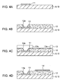
- FIGS. 4A to 4M A typical example of a method of manufacturing a printed wiring board with a component mounting pin will be described with reference to FIGS. 4A to 4M in conjunction with a method using plating (plating method).
- this manufacturing method is characterized by a component mounting pin using an outermost conductor 11, other portions (see reference numerals 9 and 10 in FIGS. 1 to 3 ) than the outermost conductor 11 were already formed.
- FIG. 4A is a diagram showing a process for preparing a substrate (portions other than the outermost conductor) 9, 10.
- the substrates 9 and 10 are composed of printed wiring boards in which portions other than the outermost conductor 11 are formed.
- the outermost conductor 11 is formed by a full-additive method, a semi-additive method or by a subtractive method.
- a semiconductor device connection land having a thickness of 20 ⁇ m, a diameter (diameter of conductive land) of 150 ⁇ m and a minimum pitch (distance between the adjacent conductive lands) of 200 ⁇ m is formed as this outermost conductor 11.
- Placement of the conductive land 11 is such one that a central portion is a lattice-like placement, an outer peripheral portion being a random placement.
- the number of the conductive land 11 amounts to approximately 50 x 40.
- Such conductive land group is formed within an area of about 150 square mm at the outermost layer of the printed wiring board.
- FIG. 4B is a diagram showing a process for forming a solder resist layer.
- a solder resist layer 12 is coated on the conductive land 11 by screen printing and an opening portion 12a is formed on the solder resist layer 12.
- a semi-cured insulating film may be attached to the substrate 9, 10 and the opening portion 12a may be formed on the insulating film by using laser light or the like after the insulating film was cured.
- FIG. 4C is a diagram showing a process in which a resist is laminated, exposed and developed.
- a dry film 13 for example, is laminated on the solder resist layer 12 and an opening portion 13a is formed on the dry film 13 by exposure and development.
- the opening portion 13a is formed on the dry film 13 at the proper position so as not to overlap with the opening portion 12a on the solder resist layer 12 in the thickness direction.
- FIG. 4D is a diagram showing a process in which a Sn (tin) layer is formed.
- a Sn layer 14 for example, is deposited on the solder resist layer 12 of the bottoms of the dry film 13 and the opening portion 13a by sputtering. After that, the dry film 13 is removed from the solder resist layer 12. As a result, only the Sn layer 14 is left on the solder resist layer 12 of the bottom of the opening portion 13a.
- This Sn layer 14 is partly removed by an etching process shown in FIG. 4K and therefore referred to as a "sacrificial layer".
- a catalytic nucleus (not shown) for use in electroless plating is given to the resultant product.
- Noble metal ion and noble metal colloid e.g. palladium chloride and palladium colloid
- FIG. 4E is a diagram showing a process for forming a first plated layer.
- a first plating layer 16 may be typically formed by electroless copper plating.
- an electroless plating bath may employ tartaric acid as a complexing agent and it may further contain at least one kind of metal ions as an additive.
- the first plating layer is believed to be under tensile stress by suppressing hydrogen from being generated.
- FIG. 4F is a diagram showing a process for forming a second plating layer.
- a second plating layer 17 may be typically formed by electroless copper plating.
- this electroless plating bath may contain EDTA (ethylenediaminetetracetic acid) as a complexing agent and the second layer 17 may contain a large quantity of hydrogen.
- EDTA ethylenediaminetetracetic acid
- FIG. 4G is a diagram showing a process for laminating an etching resist.
- a dry film 25 is laminated on the second plating layer 17.
- FIG. 4H is a diagram showing a process for exposing and developing the etching resist 25. According to this process shown in FIG. 4H , there is formed the etching resist 25 for use with the next etching process.
- FIG. 4I is a diagram showing an etching process for etching the first and second plating layers 16 and 17.
- the etching resist 25 is used to etch the first and second plating layers 16 and 17, each of which is the electroless plating layer, to form a conductive land (pattern). Thereafter, the etching resist 25 is stripped from the second plating layer 17.
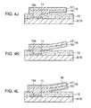
- FIG. 4J is a diagram showing an etching process of the Sn layer 14. As shown in FIG. 4J , the Sn layer 14 located under the first plating layer 16 is partly etched away by using a Sn stripping agent.
- FIG. 4K is a diagram showing a process for forming a component mounting pin.
- the Sn layer 14 located under the first plating layer 16 is removed and thereby the component mounting pin 18 is formed. Since this component mounting pin 18 is formed by the bilayer structure composed of the first plating layer 16 which is easy to expand with tensile stress and the second plating layer 17 which is easy to contract with compressive stress, the first plating layer 16 expands and the second plating layer 17 contracts to cause this component mounting pin 18 to erect upward.
- FIG. 4L is a diagram showing a process for forming a protective film.
- a desired protective film (coating) 19 is formed on the component mounting pin 18 if necessary.
- Either a coating of a single layer or coatings of a plurality of layers selected from Ni, Au, Cu, Pd/Sn and the like may be formed as this coating by using plating, for example.
Landscapes
- Engineering & Computer Science (AREA)
- Microelectronics & Electronic Packaging (AREA)
- Manufacturing & Machinery (AREA)
- Metallurgy (AREA)
- Electric Connection Of Electric Components To Printed Circuits (AREA)
- Structures For Mounting Electric Components On Printed Circuit Boards (AREA)
Abstract
Description
- The present invention relates to a printed wiring board with a component mounting pin and an electronic device using the same, and more particularly to a printed wiring board with a component mounting pin for use in mounting surface-mounting type parts and an electronic device using the same.
- A number of electronic components (e.g. semiconductor apparatus such IC and LSI) are employed to fabricate electronic apparatus. A printed wiring board is used to electrically connect electrode pads of these semiconductor apparatus. Since it is inevitable that highly-integrated semiconductor apparatus includes a large number of electrodes, in order to mount such semiconductor apparatus on a printed wiring board with a limited area, it is customary that a flip-chip mounting system is used to mount the electrode pads of the semiconductor chip on the printed wiring board in such a manner that their surfaces are opposed to the printed wiring board to thereby connect the electrode pads to the lands of the printed wiring board mounting surface by a suitable technology such as solder bump.
- In the document of the present application, "printed wiring board" refers to a board with a wiring pattern formed on an insulating substrate, and "printed circuit board" refers to a component product in which electronic components such as IC and LSI are mounted on the printed wiring board. The printed circuit board is a component product of an electronic component with predetermined objects and therefore referred to as an "electronic device".
[Patent Document 1]: Japanese Patent Laid-open Publication No.2005-183466 - The Background Art of the
Patent Document 1 has described a flip-chip mounting system printed circuit board using suitable technology such as solder bump in which a solder resist layer 70 is formed on an upper layer of a via hole 160 and a conductor circuit 158, bumps 76U and 76D being formed on the via hole 160 and the conductor circuit 158 through an opening portion 71 of the solder resist layer 70. An IC chip, not shown may be electrically connected to the printed circuit board by C4 (flip-chip) mounting. - However, the
above Patent Document 1 fails to mention a printed wiring board with a component mounting pin disclosed in the present application. - On the other hand, as integration degree of semiconductor apparatus is increasing more in recent years, a chip size thereof also is becoming enormous. If an electronic device in the mounting state in which an electrode pad of an electronic component (e.g. semiconductor chip) of a gigantic size and a land of a printed wiring board are soldered is exposed to rise and fall of an ambient temperature, then there is the possibility that a soldered portion will be broken due to a difference between coefficients of thermal expansion of the electronic component and the printed wiring board.
- Therefore, a demand of developing a printed wiring board in which malconnection or disconnection caused by a difference between the coefficients of thermal expansion of the electronic component and the printed wiring board can be decreased even when a highly-integrated semiconductor chip is mounted thereon has increased so far.
- In view of the aforesaid aspects, the present invention intends to provide a printed wiring board in which malconnection or disconnection caused by a difference between the coefficients of thermal expansion of an electronic component and a printed wiring board can be decreased even when a highly-integrated electronic component is mounted thereon.
- Further, the present invention intends to provide an electronic device in which malconnection or disconnection caused by a difference between the coefficients of thermal expansion of a semiconductor chip and a printed wiring board can be decreased even when a highly-integrated electronic component is mounted thereon.
- In the light of the above matters, a printed wiring board of the present invention includes component mounting pin.
- Further, in the printed wiring board, said component mounting pin may be elongated from an outermost conductor of said printed wiring board and the other end thereof may be erected from said printed wiring board.
- Further, in the printed wiring board, said component mounting pin may be made of an elastic material.
- Further, in the printed wiring board, said component mounting pin may be made of a material with low electric resistance.
- Further, in the printed wiring board, said component mounting pin may be made of any material selected from a group consisting of a metal, a conductive rubber, a partly-conductive rubber, a conductive synthetic resin and a partly-conductive synthetic resin.
- Further, in the printed wiring board, said component mounting pin may be formed of films of n layers (n≧2) and a film of a first layer is easy to expand relative to a film of an nth layer where a film located on the side opposing to said printed wiring board is expressed as n=1.
- Further, in the printed wiring board, stress of an n-1th layer may be tensile stress relative to stress of said nth layer or it is equal to the stress of said nth layer, and stress of said first layer may be tensile stress relative to the stress of said nth layer.
- Further, in the printed wiring board, said n-1th layer may have an equal or higher coefficient of thermal expansion to or than that of thermal expansion of said nth layer, and said first layer may have a higher coefficient of thermal expansion than that of thermal expansion of said nth layer.
- Further, in the printed wiring board, said component mounting pin may have a conductive protective coating formed thereon.
- Further, in the printed wiring board, said component mounting pin may have a solder bump formed at its tip end portion.
- Further, an electronic device of the present invention comprises: a printed wiring board with a component mounting pin; and a surface-mounting type component with an electrode pad, wherein said component mounting pin is electrically connected to said electrode pad.
- Further, in the electronic device, said component mounting pin may have elasticity and may be urged against said electrode pad.
- Further, in the electronic device, said component mounting pin may be short in length.
- Further, in the electronic device, said component mounting pin may be elongated from an outermost conductor of said printed wiring board, erected upward and connected to said electrode pad and the portion in which said component mounting pin ma be erected upward is enclosed by the air.
- Further, an electronic device of the present invention comprises: a printed wiring board with a component mounting pin; and a surface-mounting type component with an electrode pad, wherein said component mounting pin has a solder bump formed at its tip end portion and is soldered to said electrode pad.
- According to the present invention, it is possible to provide a printed wiring board in which malconnection or disconnection caused by a difference between the coefficients of thermal expansion of an electronic component and a printed wiring board can be decreased even when a highly-integrated electronic component is mounted thereon.
- Further, according to the present invention, it is possible to provide an electronic device in which malconnection or disconnection caused by a difference between the coefficients of thermal expansion of an electronic component and a printed wiring board can be decreased even when a highly-integrated electronic component is mounted thereon.
-
-
FIG. 1 is a diagram showing part of an arrangement of a printed wiring board with a component mounting pin; -
FIG. 2 is a diagram showing part of an electronic device using a printed wiring board with a component mounting pin; -
FIG. 3 is a diagram showing part of an electronic device in which electric connection is maintained between the component mounting pin of the printed wiring board and the electronic component by soldering; and -
FIGS. 4A to 4L are respectively diagrams showing respective steps of a method of manufacturing a printed wiring board with a component mounting pin. - 1:printed wiring board, 2:semiconductor apparatus (IC, LSI, etc.), 3:electrode pad, 4:electronic device, 5:filled via, 10:insulating layer, 11 outermost layer conductor, conductive land, 12:solder resist layer, 12a:opening, 13:dry film, l3a:opening, 14:Sn layer, 16:first plating layer, 17:second plating layer, 18:component mounting pin, 20:etching resist,
- A printed wiring board and an electronic device using the same according to the embodiments of the present invention will be described below in detail with reference to the accompanying drawings, wherein identical elements and parts are denoted by identical reference numerals and therefore need not be described. [ARRANGEMENTS OF PRINTED WIRING BOARD WITH COMPONENT MOUNTING PIN AND ELECTRONIC DEVICE USING THE SAME]
-
FIG. 1 of the accompanying drawings is a diagram showing part of a printed wiring board with a component mounting pin. A printedwiring board 1 according to the embodiment of the present invention includes acomponent mounting pin 18 to connect with an electronic component (not shown) like a semiconductor apparatus such as an IC and an LSI. - The printed
wiring board 1 with a component mounting pin according to the embodiment of the present invention is characterized by thecomponent mounting pin 18 electrically connected to anoutermost conductor 11. Accordingly, a rest of the arrangement of the printedwiring board 1 can be changed freely. Since the embodiment of the present invention is characterized by the outermost conductor, the printedwiring board 1 will be described such that aninsulating layer 10 with theoutermost layer conductor 11 formed thereon, asolder resist layer 12 formed on theinsulating layer 10 andother layer 9 formed under theinsulating layer 10, each of which comprises the printedwiring board 1, will be highlighted separately in order to understand the present embodiment more clearly. - For example, the printed
wiring board 1 includes thesolder resist layer 12 with an opening 12a and thesubstrates substrate 10 is the insulating layer formed under thesolder resist layer 12 and thesubstrate 9 is composed of a predetermined conductive layer and an insulating layer. Theinsulating layer 10 has a filled viahole 5 and the upper portion of the filled viahole 5 is formed as theoutermost conductor 11. - One end of the
component mounting pin 18 is electrically connected to theoutermost conductor 11 and the other end thereof is erected upward from the printedwiring board 1. Thecomponent mounting pin 18 might be covered with a desired conductiveprotective coating 19 if necessary. The printedwiring board 1 is connected to a semiconductor apparatus (not shown) by thiscomponent mounting pin 18. - The
component mounting pin 18 is made of a material having suitable properties such as flexibility, elasticity and pliability and should preferably be made of a material with low electric resistance in addition to flexibility, elasticity and pliability. This elastic material, for example, might be any material selected from a group consisting of metal, conductive rubber, partly-conductive rubber, conductive synthetic resin and partly-conductive synthetic resin. - The
component mounting pin 18 might be formed of films of n layers (n≧2 wherein a first layer is assumed to be disposed on the side opposing to the printed wiring board 1). If the film of the nth layer is easy to contract relative to the film of the first layer, the film of the nth layer need not contract relative to a film of an n-1th layer. The above film arrangement may be provided by suitable methods such as to cause the film of the nth layer to be under compressive stress relative to the film of the first layer and to cause the film of the nth layer to have a lower coefficient of thermal expansion than a coefficient of thermal expansion of the film of the first layer. - Then, the film of the n-1th layer may be under tensile stress relative to the film of the nth layer or the film of the n-th layer may be without tensile stress or compressive stress relative to the film of the nth layer. Also, the film of the n-1th layer may have a higher coefficient of thermal expansion than a coefficient of thermal expansion of the film of the nth layer or the film of the n-th layer may have an equal coefficient of thermal expansion to a coefficient of thermal expansion of the film of the nth layer. The film of the second layer may be under compressive stress relative to the film of the first layer, the film of the third layer may be under compressive stress relative to the film of the second layer, ..., the film of the nth layer may be under compressive stress relative to the film of the n-1th layer. Also, coefficients of thermal expansion of the respective layers can be lowered progressively from the first layer to the nth layer.
-
FIG. 2 is a diagram showing part of theelectronic device 4 using the printedwiring board 1 with thecomponent mounting pin 18, revealing the mounting structure. As shown inFIG. 2 , thecomponent mounting pin 18 of the printedwiring board 1 mechanically contacts with theelectrode pad 3 formed on theelectronic component 2 like the semiconductor apparatus such as IC and LSI to maintain electric connection between it and theelectronic component 2. - The printed
wiring board 1 and thesemiconductor apparatus 2 might be fixed to each other by any method. Although not shown, both of the printedwiring board 1 and thesemiconductor apparatus 2 may be fixed to a casing of the electronic device, for example. Alternatively, both of the printedwiring board 1 and thesemiconductor apparatus 2 may be fixed to each other by adhesive such as resin. - This
electronic device 4 is characterized in that a member to connect theelectronic component 2 and the printedwiring board 1 is changed from the related-art solder bump (not shown) to thecomponent mounting pin 18. - Since the
component mounting pin 18 has suitable properties such as flexibility, elasticity and pliability, when thecomponent mounting pin 18 is pressed against theelectrode pad 3, it can assure electric connection between thesemiconductor apparatus 2 and the printedwiring board 1. Further, thecomponent mounting pin 18 is a machine element that can absorb force (mechanical energy) applied to either of or both of thesemiconductor apparatus 2 and the printedwiring board 1 by either elasticity or deformation. As a result, it is possible to decrease malconnection or disconnection caused by a difference between coefficients of thermal expansion of thesemiconductor apparatus 2 and the printedwiring board 1. - While the size of the printed
wiring board 1 is 30 to 70 mm squares, for example, it may be not limited thereto and can be changed freely. The size of thesemiconductor apparatus 2 mounted on the printedwiring board 1 is 10 to 30 mm squares, for example. Onesemiconductor apparatus 2 is provided with electrode pads with 3,000 to 20,000 attachment points. In particular, the embodiment of the present invention is suitable for mounting an electronic component including electrode pads with 10,000 to 20,000 attachment points. Although it is customary to mount onesemiconductor apparatus 2 on one printedwiring board 1, even when two or three semiconductor apparatus is mounted on the semiconductor apparatus in an MCM (Multichip module) packaged fashion, thecomponent mounting pin 18 is able to decrease malconnection or disconnection caused by a difference between coefficients of thermal expansion. - Further, the
component mounting pin 18 is very short and it is able to obtain excellent electric characteristics from standpoints of matching of characteristic impedance Z0 and increasing a propagation speed of an electric signal. Similarly, when thecomponent mounting pin 18 is made of a material with low electric resistance, it is possible to avoid useless voltage drop. For example, this is the case in which thecomponent mounting pin 18 may be made of Cu (copper), Au (gold), Ag (silver) or alloy of any combination thereof or thecomponent mounting pin 18 may be surface-finished by these metals. - Further, since the
component mounting pin 18 is erected upward from the printedwiring board 1, it can be enclosed with the air so that a signal can be transmitted at a higher speed. - Further, when the
component mounting pin 18 is brought in mechanical contact with theelectrode pad 3 under force of repulsion, it is possible to maintain electric connection between thesemiconductor apparatus 2 and the printedwiring board 1 satisfactorily. - Further, since the printed
wiring board 1 with thecomponent mounting pin 18 according to the embodiment of the present invention is characterized by thecomponent mounting pin 18 electrically connected to theoutermost conductor 11, other portions of the printedwiring board 1 can be changed freely and the present embodiment can be applied to large-sized printed wiring boards and coreless substrates which are easy to warp, etc. - Furthermore, since the
semiconductor apparatus 2 and the printedwiring board 1 are connected not by soldering but by mechanical contact made by thecomponent mounting pin 18, the present embodiment has a merit that thermal budget such as reflow will not be left. -
FIG. 3 is a diagram showing part of theelectronic device 5 in which electric connection is maintained between thecomponent mounting pin 18 of the printedwiring board 1 and thesemiconductor apparatus 2 by soldering and reveals the mounting structure. If requested, thecomponent mounting pin 18 of the printedwiring board 1 may include thesolder bump 4 formed at its tip end potion and thecomponent mounting pin 18 and theelectrode pad 3 of thesemiconductor apparatus 2 are connected by soldering through solder reflow in a state of having theelectrode pad 3 mechanically brought in contact with thesemiconductor apparatus 2 as shown inFIG. 2 . Further, if requested, the printedwiring board 1 and thesemiconductor apparatus 2 may be fixed to each other by the above-mentioned method. - A typical example of a method of manufacturing a printed wiring board with a component mounting pin will be described with reference to
FIGS. 4A to 4M in conjunction with a method using plating (plating method). - Since this manufacturing method is characterized by a component mounting pin using an
outermost conductor 11, other portions (seereference numerals FIGS. 1 to 3 ) than theoutermost conductor 11 were already formed. - Further this application will explain the typical example of a method of manufacturing a printed wiring board with a
component mounting pin 18. Concerning the details of method of manufacturing a printed wiring board with a component mounting pin, refer to the patent application (assignee reference number: PB030) filed on the same date as this application. -
Other portions outermost conductor 11 were already formed by a well-known build-up method. With respect to such printed wiring board manufacturing method, refer toJapanese Patent Laid-open Publication No. 2004-40138 Japanese Patent Laid-open Publication No. 2004-311919 - From the foregoing, it is to be appreciated that other elements and parts than the
outermost conductor 11 are omitted from the description of the following manufacturing method. -
FIG. 4A is a diagram showing a process for preparing a substrate (portions other than the outermost conductor) 9, 10. Thesubstrates outermost conductor 11 are formed. Theoutermost conductor 11 is formed by a full-additive method, a semi-additive method or by a subtractive method. A semiconductor device connection land having a thickness of 20 µm, a diameter (diameter of conductive land) of 150 µm and a minimum pitch (distance between the adjacent conductive lands) of 200 µm is formed as thisoutermost conductor 11. Placement of theconductive land 11 is such one that a central portion is a lattice-like placement, an outer peripheral portion being a random placement. The number of theconductive land 11 amounts to approximately 50 x 40. Such conductive land group is formed within an area of about 150 square mm at the outermost layer of the printed wiring board. -
FIG. 4B is a diagram showing a process for forming a solder resist layer. As shown inFIG. 4B , a solder resistlayer 12 is coated on theconductive land 11 by screen printing and anopening portion 12a is formed on the solder resistlayer 12. Alternatively, a semi-cured insulating film may be attached to thesubstrate opening portion 12a may be formed on the insulating film by using laser light or the like after the insulating film was cured. -
FIG. 4C is a diagram showing a process in which a resist is laminated, exposed and developed. As shown inFIG. 4C , adry film 13, for example, is laminated on the solder resistlayer 12 and anopening portion 13a is formed on thedry film 13 by exposure and development. Theopening portion 13a is formed on thedry film 13 at the proper position so as not to overlap with theopening portion 12a on the solder resistlayer 12 in the thickness direction. -
FIG. 4D is a diagram showing a process in which a Sn (tin) layer is formed. As shown inFIG. 4D , aSn layer 14, for example, is deposited on the solder resistlayer 12 of the bottoms of thedry film 13 and theopening portion 13a by sputtering. After that, thedry film 13 is removed from the solder resistlayer 12. As a result, only theSn layer 14 is left on the solder resistlayer 12 of the bottom of theopening portion 13a. ThisSn layer 14 is partly removed by an etching process shown inFIG. 4K and therefore referred to as a "sacrificial layer". - Thereafter, a catalytic nucleus (not shown) for use in electroless plating is given to the resultant product. Noble metal ion and noble metal colloid (e.g. palladium chloride and palladium colloid) may be typically used as an electroless plating catalytic nucleus.
-
FIG. 4E is a diagram showing a process for forming a first plated layer. Afirst plating layer 16 may be typically formed by electroless copper plating. Preferably, in order that the deposited first platinglayer 16 may become easy to expand with tensile stress, an electroless plating bath may employ tartaric acid as a complexing agent and it may further contain at least one kind of metal ions as an additive. The first plating layer is believed to be under tensile stress by suppressing hydrogen from being generated. -
FIG. 4F is a diagram showing a process for forming a second plating layer. Asecond plating layer 17 may be typically formed by electroless copper plating. Preferably, in order that the depositedsecond plating layer 17 may become easy to contract with compressive stress, this electroless plating bath may contain EDTA (ethylenediaminetetracetic acid) as a complexing agent and thesecond layer 17 may contain a large quantity of hydrogen. - As a result, a bilayer structure consisting of the
first plating layer 16 which is easy to expand with tensile stress and thesecond plating layer 17 which is easy to contract with compressive stress are formed on the solder resistlayer 12. This bilayer structure will be formed as the component mounting pin 18 (seeFIG. 1 ) through the subsequent processes. -
FIG. 4G is a diagram showing a process for laminating an etching resist. For example, adry film 25 is laminated on thesecond plating layer 17. -
FIG. 4H is a diagram showing a process for exposing and developing the etching resist 25. According to this process shown inFIG. 4H , there is formed the etching resist 25 for use with the next etching process. -
FIG. 4I is a diagram showing an etching process for etching the first and second plating layers 16 and 17. As shown inFIG. 4I , the etching resist 25 is used to etch the first and second plating layers 16 and 17, each of which is the electroless plating layer, to form a conductive land (pattern). Thereafter, the etching resist 25 is stripped from thesecond plating layer 17. -
FIG. 4J is a diagram showing an etching process of theSn layer 14. As shown inFIG. 4J , theSn layer 14 located under thefirst plating layer 16 is partly etched away by using a Sn stripping agent. -
FIG. 4K is a diagram showing a process for forming a component mounting pin. As shown inFIG. 4K , theSn layer 14 located under thefirst plating layer 16 is removed and thereby thecomponent mounting pin 18 is formed. Since thiscomponent mounting pin 18 is formed by the bilayer structure composed of thefirst plating layer 16 which is easy to expand with tensile stress and thesecond plating layer 17 which is easy to contract with compressive stress, thefirst plating layer 16 expands and thesecond plating layer 17 contracts to cause thiscomponent mounting pin 18 to erect upward. -
FIG. 4L is a diagram showing a process for forming a protective film. As shown inFIG. 4L , a desired protective film (coating) 19 is formed on thecomponent mounting pin 18 if necessary. Either a coating of a single layer or coatings of a plurality of layers selected from Ni, Au, Cu, Pd/Sn and the like may be formed as this coating by using plating, for example. - The following effects can be achieved by the above-described embodiments.
- (1) Decrease of malconnection or disconnection caused by a difference between coefficients of thermal expansion of the semiconductor chip and the printed wiring board:
- Since the semiconductor chip and the printed wiring board are connected by the component mounting pin with suitable properties such as flexibility, resiliency and pliability (mechanically joined under repulsive force of the component mounting pin), the component mounting pin is able to absorb shearing stress caused by an expansion difference generated depending on a temperature at which it is exposed so that too large stress can be prevented from being concentrated on the solder connected portion, thereby suppressing the connected portion from being either damaged or broken.
- This component mounting pin is able to absorb stress generated from every direction of 360 degrees. As a result, it is possible to provide a printed wiring board in which malconnection or disconnection caused by a difference between coefficients of thermal expansion of the semiconductor chip and the printed wiring board can be decreased.
- (2) Excellent electric characteristics:
- Since the semiconductor chip and the printed wiring board are connected by the component mounting pin using the pattern of the printed wiring board, the connection length is shortened inevitably and thereby excellent electric characteristic can be obtained. For example, in an electronic device (i.e. multichip module) in which a plurality of semiconductor bear chips are mounted on a single printed board, a component mounting pin of which length is extremely short is formed on a microstrip line of a printed wiring board designed so as to provide a constant characteristic impedance Z0 and is connected to a semiconductor chip, whereby electric defects caused by mismatching of the characteristic impedance Z0 can be decreased.
- (3) High-speed electronic device:
- Since the semiconductor chip and the printed wiring board are connected by the short component mounting pin, it is possible to provide high-speed electronic devices.
- (4) Excellent power supply to respective circuit elements of an electronic device:
- Since the semiconductor chip and the printed wiring board are connected by the component mounting pin with low electric resistance, it is possible to prevent useless voltage drop from being caused when the power is supplied to respective circuit elements of the electronic device. As the component mounting pin with low electric resistance, there can be used a component mounting pin made of Cu, Au, Ag or any alloy thereof or a component mounting pin that is surface-finished by these metals.
- (5) High-speed signal transmission:
- Since the semiconductor chip and the printed wiring board are connected by the component mounting pin erected upward in the air, high-speed signal transmission becomes possible. More specifically, while a speed at which an electric signal is transmitted through a substrate such as a glass-epoxy substrate of which dielectric constant εr is greater than 1 is expressed as v = c/(εr)1/2 (m/s), the above speed at which an electric signal is transmitted through the component mounting pin erected upward in the air can be considered as a speed substantially close to a speed in the vacuum and can be increased more as shown by an equation expressed as v = c (m/s).
- (6) Excellent electric connection between the semiconductor chip and the printed wiring board:
- In the
electronic device 4 including the component mounting pin pressure contact mounting structure described with reference toFIG. 2 , since the semiconductor chip and the printed wiring board are mechanically joined together under repulsive force of the component mounting pin, it is possible to obtain electric connection in a state in which contact resistance is relatively low.
- In the
- (7) Applicable to relatively large printed wiring boards:
- In the
electronic device 4 including the component mounting pin pressure contact mounting structure described with reference toFIG. 2 , electric connection between the semiconductor chip and the printed wiring board can be maintained by urging the printed wiring board against the semiconductor chip. Accordingly, it is possible to realize the electronic device including the component mounting pin pressure contact mounting structure by even a printed wiring board that may warp relatively much, such as a coreless substrate without core substrate and a substrate with a thin core substrate.
- In the
- (8) Easy modification and easy repair:
- In the
electronic device 4 including the component mounting pin pressure contact mounting structure described with reference toFIG. 2 , since the semiconductor chip and the printed wiring board are not connected by soldering, the semiconductor chip and the printed wiring board can be separated with ease in a work such as modification and repair.
- In the
- (9) Printed wiring board free from damage due to heat:
- In the
electronic device 4 including the component mounting pin pressure contact mounting structure described with reference toFIG. 2 , since the semiconductor chip and the printed wiring board are not connected by soldering, thermal budget such as reflow process can be prevented from being left on the printed wiring board. That is, the printed wiring board can be protected from being damaged due to heat.
- In the
- (10) High-density pattern of printed wiring board:
- In the
electronic device 4 including the component mounting pin pressure contact mounting structure described with reference toFIG. 2 , thermal budget such as reflow process is not left on the printed wiring board. Also, the printed wiring board can be protected from being damaged due to heat and the pattern of the printed wiring board can be increased in density (pattern of the printed wiring board can be made fine). - More specifically, a reflow temperature is the highest temperature in temperatures at which the printed wiring board is exposed, and various restrictions are imposed on the printed wiring board from a design standpoint so that the printed wiring board can cope with stress upon reflow. For example, a build-up printed wiring board needs a conductor roughing treatment process to increase a bottom diameter of a via hole greater than a predetermined value (e.g. greater than 60 µm) or to increase a thickness of a conductive layer greater than a predetermined value (e.g. greater than 2 µm) in order to maintain the insulating layer and the conductive layer closely contacted with each other. However, when the reflow process becomes unnecessary, the above-mentioned restrictions can be removed and the diameter of the via hole can be reduced more. Also, since the conductor roughing treatment can be made more delicate, the pattern of the printed wiring board can be increased in density or the conductor roughing treatment can be removed (i.e. conductor surface is smooth).
- In the
- While the embodiments of the printed wiring board with the component mounting pin and the electronic device using the same have been described so far, these embodiments are described by way of example and the present invention is not limited thereto.
Addition, deletion, improvement and the like that can be made by those skilled in the art may be included in the scope of the present invention. - The technical scope of the present invention is determined by the description of the appended claims.
- It should be understood by those skilled in the art that various modifications, combinations, sub-combinations and alterations may occur depending on design requirements and other factors insofar as they are within the scope of the appended claims or the equivalents thereof.
Claims (15)
- A printed wiring board including a component mounting pin.
- A printed wiring board according to claim 1,
wherein said component mounting pin is elongated from an outermost conductor of said printed wiring board and the other end thereof is erected from said printed wiring board. - A printed wiring board according to claim 1,
wherein said component mounting pin is made of an elastic material. - A printed wiring board according to claim 1,
wherein said component mounting pin is made of a material with low electric resistance. - A printed wiring board according to claim 1,
wherein said component mounting pin is made of any material selected from a group consisting of a metal, a conductive rubber, a partly-conductive rubber, a conductive synthetic resin and a partly-conductive synthetic resin. - A printed wiring board according to claim 1,
wherein said component mounting pin is formed of films of n layers (n≧2) and a film of a first layer is easy to expand relative to a film of an nth layer where a film located on the side opposing to said printed wiring board is expressed as n = 1. - A printed wiring board according to claim 6,
wherein stress of an n-1th layer is tensile stress relative to stress of said nth layer or it is equal to the stress of said nth layer, and
stress of said first layer is tensile stress relative to the stress of said nth layer. - A printed wiring board according to claim 6,
wherein said n-1th layer has an equal or higher coefficient of thermal expansion to or than that of thermal expansion of said nth layer, and
said first layer has a higher coefficient of thermal expansion than that of thermal expansion of said nth layer. - A printed wiring board according to claim 1,
wherein said component mounting pin has a conductive protective coating formed thereon. - A printed wiring board according to claim 1,
wherein said component mounting pin has a solder bump formed at its tip end portion. - An electronic device comprising:a printed wiring board with a component mounting pin; anda surface-mounting type component with an electrode pad, wherein said component mounting pin is electrically connected to said electrode pad.
- An electronic device according to claim 11,
wherein said component mounting pin has elasticity and is urged against said electrode pad. - An electronic device according to claim 11,
wherein said component mounting pin is short in length. - An electronic device according to claim 11,
wherein said component mounting pin is elongated from an outermost conductor of said printed wiring board, erected upward and connected to said electrode pad and the portion in which said component mounting pin is erected upward is enclosed by the air. - An electronic device comprising:a printed wiring board with a component mounting pin; anda surface-mounting type component with an electrode pad, wherein said component mounting pin has a solder bump formed at its tip end portion and is soldered to said electrode pad.
Applications Claiming Priority (2)
| Application Number | Priority Date | Filing Date | Title |
|---|---|---|---|
| JP2005356049A JP4848752B2 (en) | 2005-12-09 | 2005-12-09 | Printed wiring board having component mounting pins and electronic device using the same |
| PCT/JP2006/323913 WO2007066563A1 (en) | 2005-12-09 | 2006-11-30 | Printed wiring board with component-mounting pins and electronic equipment using the same |
Publications (2)
| Publication Number | Publication Date |
|---|---|
| EP1895821A1 true EP1895821A1 (en) | 2008-03-05 |
| EP1895821A4 EP1895821A4 (en) | 2010-11-17 |
Family
ID=38122708
Family Applications (1)
| Application Number | Title | Priority Date | Filing Date |
|---|---|---|---|
| EP06833716A Ceased EP1895821A4 (en) | 2005-12-09 | 2006-11-30 | PRINTED WIRING BOARD WITH COMPONENT MOUNTING PINS AND ELECTRONIC EQUIPMENT HAVING THIS CARD |
Country Status (7)
| Country | Link |
|---|---|
| US (1) | US7773388B2 (en) |
| EP (1) | EP1895821A4 (en) |
| JP (1) | JP4848752B2 (en) |
| KR (1) | KR20070100386A (en) |
| CN (1) | CN101189922A (en) |
| TW (1) | TWI341153B (en) |
| WO (1) | WO2007066563A1 (en) |
Families Citing this family (8)
| Publication number | Priority date | Publication date | Assignee | Title |
|---|---|---|---|---|
| JP2007165383A (en) | 2005-12-09 | 2007-06-28 | Ibiden Co Ltd | Printed circuit board with component mounting pins |
| JP4848752B2 (en) | 2005-12-09 | 2011-12-28 | イビデン株式会社 | Printed wiring board having component mounting pins and electronic device using the same |
| JP4654897B2 (en) | 2005-12-09 | 2011-03-23 | イビデン株式会社 | Method for manufacturing printed wiring board having component mounting pins |
| US8382487B2 (en) * | 2010-12-20 | 2013-02-26 | Tyco Electronics Corporation | Land grid array interconnect |
| JP5794850B2 (en) * | 2011-07-26 | 2015-10-14 | 新光電気工業株式会社 | Manufacturing method of connection terminal structure |
| TWI574473B (en) * | 2012-06-07 | 2017-03-11 | 鴻海精密工業股份有限公司 | Electrical connector assembly |
| FR3009445B1 (en) * | 2013-07-31 | 2017-03-31 | Hypertac Sa | CONTACT MEMBER BETWEEN A SUPPORT AND A DEVICE AND ELECTRICAL CONNECTOR COMPRISING SUCH A CONTACT MEMBER |
| CN106028624B (en) * | 2016-06-28 | 2018-12-04 | 广东欧珀移动通信有限公司 | Elastic slice, pcb board and the mobile terminal of pcb board |
Family Cites Families (39)
| Publication number | Priority date | Publication date | Assignee | Title |
|---|---|---|---|---|
| US4828346A (en) | 1985-10-08 | 1989-05-09 | The Boc Group, Inc. | Transparent article having high visible transmittance |
| US6043563A (en) | 1997-05-06 | 2000-03-28 | Formfactor, Inc. | Electronic components with terminals and spring contact elements extending from areas which are remote from the terminals |
| US5476211A (en) * | 1993-11-16 | 1995-12-19 | Form Factor, Inc. | Method of manufacturing electrical contacts, using a sacrificial member |
| US5719448A (en) * | 1989-03-07 | 1998-02-17 | Seiko Epson Corporation | Bonding pad structures for semiconductor integrated circuits |
| WO1991013533A1 (en) * | 1990-03-01 | 1991-09-05 | Motorola, Inc. | Selectively releasing conductive runner and substrate assembly |
| JP2948039B2 (en) * | 1992-12-28 | 1999-09-13 | 株式会社日立製作所 | Circuit board |
| JPH077263A (en) | 1993-06-14 | 1995-01-10 | Nippon Avionics Co Ltd | Jumper wiring bonding method and device |
| US6835898B2 (en) * | 1993-11-16 | 2004-12-28 | Formfactor, Inc. | Electrical contact structures formed by configuring a flexible wire to have a springable shape and overcoating the wire with at least one layer of a resilient conductive material, methods of mounting the contact structures to electronic components, and applications for employing the contact structures |
| JP2986677B2 (en) | 1994-06-02 | 1999-12-06 | 富士通株式会社 | Ultrasonic thermocompression bonding equipment |
| DE4437260C1 (en) * | 1994-10-18 | 1995-10-19 | Siemens Ag | Micro-mechanical electrostatic relay with slotted spring tongue surface |
| US5495667A (en) * | 1994-11-07 | 1996-03-05 | Micron Technology, Inc. | Method for forming contact pins for semiconductor dice and interconnects |
| US5613861A (en) * | 1995-06-07 | 1997-03-25 | Xerox Corporation | Photolithographically patterned spring contact |
| CN1094717C (en) * | 1995-11-16 | 2002-11-20 | 松下电器产业株式会社 | PC board and fixing body thereof |
| KR100577132B1 (en) * | 1997-05-15 | 2006-05-09 | 폼팩터, 인크. | Microelectronic Contact Structures and Methods for Manufacturing and Using Them |
| US6245444B1 (en) | 1997-10-02 | 2001-06-12 | New Jersey Institute Of Technology | Micromachined element and method of fabrication thereof |
| JPH11326379A (en) * | 1998-03-12 | 1999-11-26 | Fujitsu Ltd | Contactor for electronic component, method of manufacturing the same, and contactor manufacturing apparatus |
| CN1276259C (en) * | 1998-12-02 | 2006-09-20 | 佛姆法克特股份有限公司 | Photolithographic contact elements |
| JP4458582B2 (en) | 1999-01-04 | 2010-04-28 | イビデン株式会社 | Package substrate |
| WO2000045430A1 (en) * | 1999-01-29 | 2000-08-03 | Matsushita Electric Industrial Co., Ltd. | Electronic parts mounting method and device therefor |
| US6229683B1 (en) * | 1999-06-30 | 2001-05-08 | Mcnc | High voltage micromachined electrostatic switch |
| US6827584B2 (en) * | 1999-12-28 | 2004-12-07 | Formfactor, Inc. | Interconnect for microelectronic structures with enhanced spring characteristics |
| US6396677B1 (en) | 2000-05-17 | 2002-05-28 | Xerox Corporation | Photolithographically-patterned variable capacitor structures and method of making |
| KR20010112575A (en) | 2000-06-09 | 2001-12-20 | 송길봉 | Automatic valve |
| US6290510B1 (en) * | 2000-07-27 | 2001-09-18 | Xerox Corporation | Spring structure with self-aligned release material |
| JP2003013247A (en) | 2001-04-24 | 2003-01-15 | Murata Mfg Co Ltd | Electroless copper plating bath and electronic component for high frequency |
| US6560861B2 (en) * | 2001-07-11 | 2003-05-13 | Xerox Corporation | Microspring with conductive coating deposited on tip after release |
| JP2003198068A (en) | 2001-12-27 | 2003-07-11 | Nec Corp | Printed circuit board, semiconductor device, and electrical connection structure between printed circuit board and components |
| JP2004311919A (en) | 2003-02-21 | 2004-11-04 | Shinko Electric Ind Co Ltd | Through hole fill method |
| JP2004040138A (en) | 2003-10-27 | 2004-02-05 | Ibiden Co Ltd | Build up multilayer printed circuit board |
| US7160121B2 (en) * | 2003-12-15 | 2007-01-09 | Palo Alto Research Center Incorporated | Stressed metal contact with enhanced lateral compliance |
| JP2005183466A (en) | 2003-12-16 | 2005-07-07 | Ibiden Co Ltd | Multilayer printed wiring board |
| US7459795B2 (en) * | 2004-08-19 | 2008-12-02 | Formfactor, Inc. | Method to build a wirebond probe card in a many at a time fashion |
| US7230440B2 (en) * | 2004-10-21 | 2007-06-12 | Palo Alto Research Center Incorporated | Curved spring structure with elongated section located under cantilevered section |
| JP4559936B2 (en) | 2004-10-21 | 2010-10-13 | アルプス電気株式会社 | Electroless plating method and circuit forming method using this method |
| JP2006208358A (en) * | 2004-12-28 | 2006-08-10 | Tdk Corp | Sensor |
| US7449779B2 (en) * | 2005-03-22 | 2008-11-11 | Tessera, Inc. | Wire bonded wafer level cavity package |
| JP4848752B2 (en) | 2005-12-09 | 2011-12-28 | イビデン株式会社 | Printed wiring board having component mounting pins and electronic device using the same |
| JP2007165383A (en) * | 2005-12-09 | 2007-06-28 | Ibiden Co Ltd | Printed circuit board with component mounting pins |
| US7530814B2 (en) * | 2007-09-25 | 2009-05-12 | Intel Corporation | Providing variable sized contacts for coupling with a semiconductor device |
-
2005
- 2005-12-09 JP JP2005356049A patent/JP4848752B2/en not_active Expired - Fee Related
-
2006
- 2006-11-30 EP EP06833716A patent/EP1895821A4/en not_active Ceased
- 2006-11-30 CN CNA2006800091042A patent/CN101189922A/en active Pending
- 2006-11-30 WO PCT/JP2006/323913 patent/WO2007066563A1/en not_active Ceased
- 2006-11-30 KR KR1020077019656A patent/KR20070100386A/en not_active Ceased
- 2006-12-05 US US11/566,912 patent/US7773388B2/en not_active Expired - Fee Related
- 2006-12-08 TW TW095146065A patent/TWI341153B/en active
Also Published As
| Publication number | Publication date |
|---|---|
| TW200806133A (en) | 2008-01-16 |
| CN101189922A (en) | 2008-05-28 |
| US7773388B2 (en) | 2010-08-10 |
| EP1895821A4 (en) | 2010-11-17 |
| WO2007066563A1 (en) | 2007-06-14 |
| JP2007165373A (en) | 2007-06-28 |
| JP4848752B2 (en) | 2011-12-28 |
| US20070187140A1 (en) | 2007-08-16 |
| TWI341153B (en) | 2011-04-21 |
| KR20070100386A (en) | 2007-10-10 |
Similar Documents
| Publication | Publication Date | Title |
|---|---|---|
| US6803664B2 (en) | Semiconductor package | |
| US7923367B2 (en) | Multilayer wiring substrate mounted with electronic component and method for manufacturing the same | |
| US6236115B1 (en) | High density integrated circuit packaging with chip stacking and via interconnections | |
| KR102163039B1 (en) | Printed circuit board and method of manufacturing the same, and electronic component module | |
| EP1207727B1 (en) | Compliant laminate connector | |
| US20170250141A1 (en) | Wiring circuit board, semiconductor device, method of manufacturing wiring circuit board, and method of manufacturing semiconductor device | |
| US10714416B2 (en) | Semiconductor package having a circuit pattern | |
| WO2012040724A1 (en) | Electrolytic depositon and via filling in coreless substrate processing | |
| CN104718802A (en) | The printed circuit board and the method for manufacturing the same | |
| US6596620B2 (en) | BGA substrate via structure | |
| KR101109261B1 (en) | Printed circuit board and manufacturing method thereof | |
| US20110147058A1 (en) | Electronic device and method of manufacturing electronic device | |
| US7773388B2 (en) | Printed wiring board with component mounting pin and electronic device using the same | |
| KR101167453B1 (en) | A printed circuit board comprising embeded electronic component within and a method for manufacturing | |
| JP4528715B2 (en) | Semiconductor device and manufacturing method thereof | |
| KR20180077115A (en) | Manufacturing method of pcb and semiconductor package using transparent carrier | |
| US8409461B2 (en) | Method of manufacturing printed wiring board with component mounting pin | |
| US20110061907A1 (en) | Printed circuit board and method of manufacturing the same | |
| CN115020369A (en) | Circuit board assembly, method of manufacturing the same, and electronic apparatus | |
| JP2024160760A (en) | Wiring board for mounting semiconductor device and manufacturing method thereof | |
| JP2002076592A (en) | Printed wiring board and its producing method | |
| KR20100125787A (en) | Printed Circuit Board with Solder Pattern and Manufacturing Method Thereof | |
| HK1188030A (en) | Electrolytic deposition and via filling in coreless substrate processing | |
| JP2012023364A (en) | Method for manufacturing semiconductor package substrate |
Legal Events
| Date | Code | Title | Description |
|---|---|---|---|
| PUAI | Public reference made under article 153(3) epc to a published international application that has entered the european phase |
Free format text: ORIGINAL CODE: 0009012 |
|
| 17P | Request for examination filed |
Effective date: 20070521 |
|
| AK | Designated contracting states |
Kind code of ref document: A1 Designated state(s): AT BE BG CH CY CZ DE DK EE ES FI FR GB GR HU IE IS IT LI LT LU LV MC NL PL PT RO SE SI SK TR |
|
| DAX | Request for extension of the european patent (deleted) | ||
| A4 | Supplementary search report drawn up and despatched |
Effective date: 20101014 |
|
| 17Q | First examination report despatched |
Effective date: 20110617 |
|
| DAX | Request for extension of the european patent (deleted) | ||
| REG | Reference to a national code |
Ref country code: DE Ref legal event code: R003 |
|
| STAA | Information on the status of an ep patent application or granted ep patent |
Free format text: STATUS: THE APPLICATION HAS BEEN REFUSED |
|
| 18R | Application refused |
Effective date: 20131016 |