EP1895669A2 - RFIC with On-chip acoustic transducer circuit - Google Patents
RFIC with On-chip acoustic transducer circuit Download PDFInfo
- Publication number
- EP1895669A2 EP1895669A2 EP07008692A EP07008692A EP1895669A2 EP 1895669 A2 EP1895669 A2 EP 1895669A2 EP 07008692 A EP07008692 A EP 07008692A EP 07008692 A EP07008692 A EP 07008692A EP 1895669 A2 EP1895669 A2 EP 1895669A2
- Authority
- EP
- European Patent Office
- Prior art keywords
- signals
- transmit
- receive
- digital
- convert
- Prior art date
- Legal status (The legal status is an assumption and is not a legal conclusion. Google has not performed a legal analysis and makes no representation as to the accuracy of the status listed.)
- Granted
Links
Images





Classifications
-
- H—ELECTRICITY
- H04—ELECTRIC COMMUNICATION TECHNIQUE
- H04B—TRANSMISSION
- H04B1/00—Details of transmission systems, not covered by a single one of groups H04B3/00 - H04B13/00; Details of transmission systems not characterised by the medium used for transmission
- H04B1/06—Receivers
- H04B1/16—Circuits
- H04B1/30—Circuits for homodyne or synchrodyne receivers
-
- H—ELECTRICITY
- H10—SEMICONDUCTOR DEVICES; ELECTRIC SOLID-STATE DEVICES NOT OTHERWISE PROVIDED FOR
- H10D—INORGANIC ELECTRIC SEMICONDUCTOR DEVICES
- H10D99/00—Subject matter not provided for in other groups of this subclass
-
- H—ELECTRICITY
- H10—SEMICONDUCTOR DEVICES; ELECTRIC SOLID-STATE DEVICES NOT OTHERWISE PROVIDED FOR
- H10D—INORGANIC ELECTRIC SEMICONDUCTOR DEVICES
- H10D89/00—Aspects of integrated devices not covered by groups H10D84/00 - H10D88/00
-
- H—ELECTRICITY
- H04—ELECTRIC COMMUNICATION TECHNIQUE
- H04B—TRANSMISSION
- H04B1/00—Details of transmission systems, not covered by a single one of groups H04B3/00 - H04B13/00; Details of transmission systems not characterised by the medium used for transmission
- H04B1/38—Transceivers, i.e. devices in which transmitter and receiver form a structural unit and in which at least one part is used for functions of transmitting and receiving
-
- H—ELECTRICITY
- H04—ELECTRIC COMMUNICATION TECHNIQUE
- H04R—LOUDSPEAKERS, MICROPHONES, GRAMOPHONE PICK-UPS OR LIKE ACOUSTIC ELECTROMECHANICAL TRANSDUCERS; ELECTRIC HEARING AIDS; PUBLIC ADDRESS SYSTEMS
- H04R19/00—Electrostatic transducers
- H04R19/005—Electrostatic transducers using semiconductor materials
Definitions
- This invention relates generally to wireless communication systems and more particularly to wireless communication devices.
- Communication systems are known to support wireless and wire lined communications between wireless and/or wire lined communication devices. Such communication systems range from national and/or international cellular telephone systems to the Internet to point-to-point in-home wireless networks. Each type of communication system is constructed, and hence operates, in accordance with one or more communication standards. For instance, wireless communication systems may operate in accordance with one or more standards including, but not limited to, IEEE 802.11, Bluetooth, ZigBee, advanced mobile phone services (AMPS), digital AMPS, global system for mobile communications (GSM), code division multiple access (CDMA), local multi-point distribution systems (LMDS), multi-channel-multi-point distribution systems (MMDS), radio frequency identification (RFID), and/or variations thereof.
- GSM global system for mobile communications
- CDMA code division multiple access
- LMDS local multi-point distribution systems
- MMDS multi-channel-multi-point distribution systems
- RFID radio frequency identification
- a wireless communication device such as a cellular telephone, two-way radio, personal digital assistant (PDA), personal computer (PC), laptop computer, home entertainment equipment, RFID reader, RFID tag, et cetera communicates directly or indirectly with other wireless communication devices.
- PDA personal digital assistant
- PC personal computer
- laptop computer home entertainment equipment
- RFID reader RFID tag
- et cetera communicates directly or indirectly with other wireless communication devices.
- the participating wireless communication devices tune their receivers and transmitters to the same channel or channels (e.g., one of the plurality of radio frequency (RF) carriers of the wireless communication system or a particular RF frequency for some systems) and communicate over that channel(s).
- RF radio frequency
- each wireless communication device communicates directly with an associated base station (e.g., for cellular services) and/or an associated access point (e.g., for an in-home or in-building wireless network) via an assigned channel.
- an associated base station e.g., for cellular services
- an associated access point e.g., for an in-home or in-building wireless network
- the associated base stations and/or associated access points communicate with each other directly, via a system controller, via the public switch telephone network, via the Internet, and/or via some other wide area network.
- each wireless communication device For each wireless communication device to participate in wireless communications, it includes a built-in radio transceiver (i.e., receiver and transmitter) or is coupled to an associated radio transceiver (e.g., a station for in-home and/or in-building wireless communication networks, RF modem, etc.).
- the receiver is coupled to the antenna and includes a low noise amplifier, one or more intermediate frequency stages, a filtering stage, and a data recovery stage.
- the low noise amplifier receives inbound RF signals via the antenna and amplifies then.
- the one or more intermediate frequency stages mix the amplified RF signals with one or more local oscillations to convert the amplified RF signal into baseband signals or intermediate frequency (IF) signals.
- the filtering stage filters the baseband signals or the IF signals to attenuate unwanted out of band signals to produce filtered signals.
- the data recovery stage recovers raw data from the filtered signals in accordance with the particular wireless communication standard.
- the transmitter includes a data modulation stage, one or more intermediate frequency stages, and a power amplifier.
- the data modulation stage converts raw data into baseband signals in accordance with a particular wireless communication standard.
- the one or more intermediate frequency stages mix the baseband signals with one or more local oscillations to produce RF signals.
- the power amplifier amplifies the RF signals prior to transmission via an antenna.
- the raw data that is transmitted and/or received includes digitized audio signals (e.g., digitized voice, music files such as MP3 files, video files such as MPEG files, and/or a combination thereof).
- digitized audio signals e.g., digitized voice, music files such as MP3 files, video files such as MPEG files, and/or a combination thereof.
- a microphone is used to capture analog audio signals and a speaker is used to render analog audio signals audible.
- analog audio signals captured by a microphone are biased to a particular level, amplified, and digitized (i.e., converted to digital signals and may further be encoded in accordance with an encoding format).
- digitized audio signals are converted to analog audio signals, amplified via a volume control, and subsequently rendered audible by a speaker.
- MCMs Microelectromechanical Systems
- AKU1000 analog microphone chip
- AKU2000 digital microphone chip
- speaker chips While integrated microphone chips and speaker chips offer communication device manufacturers smaller form factors, the chips are still separate components requiring printed circuit board (PCB) space and connections to and/or from other integrated circuits on the PCB.
- PCB printed circuit board
- the present invention is directed to apparatus and methods of operation that are further described in the following Brief Description of the Drawings, the Detailed Description of the Invention, and the claims.
- a radio frequency integrated circuit comprises:
- the transmit acoustic transducer circuit comprises:
- the transducer comprises at least one of:
- the transmit acoustic transducer circuit comprises:
- the receive acoustic transducer circuit comprises:
- the transducer comprises at least one of:
- the receive acoustic transducer circuit comprises:
- the digital conversion module comprises:
- audio encoding module comprises:
- the digital conversion module comprises:
- the digital conversion module further comprises:
- the digital conversion module further comprises:
- the digital conversion module comprises:
- the analog conversion module comprises:
- the amplifier is further coupled to:
- audio decoding module comprises:
- the analog conversion module comprises:
- analog conversion module further comprises:
- analog conversion module further comprises:
- the RFIC further comprises:
- a radio transmitter integrated circuit comprises:
- the RTIC further comprises:
- the transmit acoustic transducer circuit comprises:
- the transmit acoustic transducer circuit comprises:
- the digital conversion module comprises:
- audio encoding module comprises:
- the analog conversion module comprises:
- analog conversion module further comprises:
- a radio receiver integrated circuit comprises:
- the RRIC further comprises:
- the receive acoustic transducer circuit comprises:
- the receive acoustic transducer circuit comprises:
- the digital conversion module comprises:
- the digital conversion module further comprises:
- the analog conversion module comprises:
- audio decoding module comprises:
- FIG. 1 is a schematic block diagram illustrating a communication system 10 that includes a plurality of base stations and/or access points 12, 16, a plurality of wireless communication devices 18-32 and a network hardware component 34.
- the network hardware 34 which may be a router, switch, bridge, modem, system controller, et cetera provides a wide area network connection 42 for the communication system 10.
- the wireless communication devices 18-32 may be laptop host computers 18 and 26, personal digital assistant hosts 20 and 30, personal computer hosts 24 and 32 and/or cellular telephone hosts 22 and 28 that include a built in radio transceiver and/or have an associated radio transceiver. The details of the radio transceiver will be described in greater detail with reference to Figures 2-16.
- Wireless communication devices 22, 23, and 24 are located within an independent basic service set (IBSS) area and communicate directly (i.e., point to point). In this configuration, these devices 22, 23, and 24 may only communicate with each other. To communicate with other wireless communication devices within the system 10 or to communicate outside of the system 10, the devices 22, 23, and/or 24 need to affiliate with one of the base stations or access points 12 or 16.
- IBSS independent basic service set
- the base stations or access points 12, 16 are located within basic service set (BSS) areas 11 and 13, respectively, and are operably coupled to the network hardware 34 via local area network connections 36, 38. Such a connection provides the base station or access point 12 16 with connectivity to other devices within the system 10 and provides connectivity to other networks via the WAN connection 42.
- BSS basic service set
- each of the base stations or access points 12-16 has an associated antenna or antenna array.
- base station or access point 12 wirelessly communicates with wireless communication devices 18 and 20 while base station or access point 16 wirelessly communicates with wireless communication devices 26 - 32.
- the wireless communication devices register with a particular base station or access point 12, 16 to receive services from the communication system 10.
- each wireless communication device includes a built-in radio and/or is coupled to a radio.
- the wireless communication devices may include an RFID reader and/or an RFID tag.
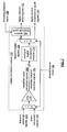
- FIG. 2 is a schematic block diagram of a radio frequency integrated circuit (RFIC) that may be used in any of the wireless communication devices of figure 1 or as a radio frequency transceiver for any other RF application where audio signals are transmitted and/or received.
- the RFIC includes a transmit acoustic transducer 100, a digital conversion module 102, a transmit baseband module 104, an analog conversion module 106, an up-conversion module 108, a power amplifier circuit 110, a low noise amplifier circuit 112, a down-conversion module 114, a receive baseband processing module 115, and a receive acoustic transducer circuit 118.
- RFIC radio frequency integrated circuit
- the transmit acoustic transducer circuit 100 (embodiments of which will be described in greater detail with reference to Figures 3 and 4) is coupled to convert transmit sound waves 118 into transmit electrical signals 120.
- the transmit sound waves 118 which may result from human speech and/or any other source that produces a wave transmitted through the air, cause mechanical vibrations within the transmit acoustic transducer circuit 100.
- the transmit acoustic transducer circuit 100 converts the mechanical vibrations into the transmit electrical signals 120.
- the digital conversion module 102 (embodiments of which will be described in greater detail with reference to Figures 7-10) is coupled to convert the transmit electrical signals 120 into digital transmit audio signals 122 when the RFIC is in a transmit mode.
- the digital transmit audio signals 122 may be encoded in accordance with one or more encoding schemes, such as Pulse Code Modulation (PCM) A-law, PCM ⁇ -law, and continuous variable slope delta demodulation.
- PCM Pulse Code Modulation
- the RFIC may be in the transmit mode via a transmit/receive mode signal 124, may be in the transmit mode in accordance with a half duplex scheme where the transmit path and receive path of the RFIC share a wireless communication resource (e.g., one or more RF channels, use the same RF carrier frequency, frequency hopping scheme, etc.), and/or may be in the transmit mode simultaneously with the receive mode when the RFIC supports a full duplex scheme where the transmit path utilizes a different wireless communication resource than the receive path.
- a wireless communication resource e.g., one or more RF channels, use the same RF carrier frequency, frequency hopping scheme, etc.
- the transmit baseband processing module 104 is coupled to convert the digital transmit audio signals 122 into digital transmit baseband or low intermediate frequency (IF) signals 126 in accordance with one or more wireless communication standards. To achieve the conversion to the digital transmit baseband or low IF signals 126, the transmit baseband processing module 104 may perform one or more transmitter functions upon the digital transmit audio signals 122.
- the transmitter functions include, but are not limited to, scrambling, encoding, puncturing, mapping, modulation, and/or digital baseband to IF conversion.
- the baseband or low IF TX signals 164 may be digital baseband signals (e.g., have a zero IF) or digital low IF signals, where the low IF typically will be in a frequency range of one hundred kilohertz to a few megahertz.
- the transmit baseband processing module 104 and the receive baseband processing module 115 may be implemented using a shared processing device, individual processing devices, or a plurality of processing devices and may further included associated memory.
- Such a processing device may be a microprocessor, microcontroller, digital signal processor, microcomputer, central processing unit, field programmable gate array, programmable logic device, state machine, logic circuitry, analog circuitry, digital circuitry, and/or any device that manipulates signals (analog and/or digital) based on operational instructions.
- the associated memory may be a single memory device or a plurality of memory devices.
- Such a memory device may be a read-only memory, random access memory, volatile memory, non-volatile memory, static memory, dynamic memory, flash memory, and/or any device that stores digital information.
- the processing module 104 and/or 116 implements one or more of its functions via a state machine, analog circuitry, digital circuitry, and/or logic circuitry
- the memory storing the corresponding operational instructions is embedded with the circuitry comprising the state machine, analog circuitry, digital circuitry, and/or logic circuitry.
- the analog conversion module 106 (embodiments of which will be described in greater detail with reference to Figures 11-14) is coupled to convert the digital transmit baseband or low IF signals 126 into analog transmit baseband or low IF signals 128 when the RFIC is in the transmit mode.
- the up-conversion module 108 is coupled to convert the analog transmit baseband or low IF signals 128, which may include in-phase components and quadrature components, into up-converted signals 132 based on a transmit local oscillation 130.
- the up-conversion module 108 may be a direct conversion module where the transmit local oscillation 130 corresponds to the difference between the IF of the analog transmit baseband or low IF signals 128 and the carrier frequency of the transmit RF signals 134.
- the up-conversion module 108 may be a superheterodyne module where the transmit local oscillation 130 includes two oscillations: one to convert the analog baseband or low IF signals 128 into intermediate frequency signals and a second to convert the intermediate frequency signals into signals having the carrier frequency of the transmit RF signals 134.
- the transmit local oscillation 130 includes an in-phase component and a quadrature component such that the quadrature component of the transmit local oscillation is mixed with the quadrature components of the analog transmit baseband or low IF signals 128 and the in-phase component of the transmit local oscillation is mixed with the in-phase components of the analog transmit baseband or low IF signals 128.
- the power amplifier circuit 110 is coupled to amplify the up-converted signals to produce the transmit radio frequency (RF) signals 134.
- the power amplifier circuit 110 may include one or more power amplifiers and/or one or more pre-amplifiers coupled in series, in parallel or combination thereof. The amplification provided by the power amplifier circuit 110 is dependent upon the desired transmit power and whether an off-chip power amplifier is used.
- the power amplifier circuit 110 provides the transmit RF signals 134 to an antenna structure for over-the-air transmission.
- the antenna structure may include a separate antenna(s) for the receive path and the transmit path of the RFIC or the transmit and receive paths may share an antenna(s) via a transmit/receive switch and/or transformer balun.
- the receive and transmit paths may share a diversity antenna structure.
- the receive and transmit paths may each have its own diversity antenna structure.
- the receive and transmit paths may share a multiple input multiple output (MIMO) antenna structure.
- MIMO multiple input multiple output
- the low noise amplifier (LNA) circuit 112 is coupled to amplify receive RF signals 136 to produce amplified receive RF signals 138.
- the LNA circuit 112 may include one or more amplifiers and/or one or more pre-amplifiers coupled in series, in parallel, or a combination thereof to amplify the receive RF signals 136 based on a gain setting.
- the gain setting is at least partially dependent upon the signal strength of the receive RF signals 136 and the desired operating range of the receive path.
- the down-conversion module 114 is coupled to convert the amplified receive RF signals 138 into the down-converted signals 142 based on a receive local oscillation 140.
- the down-conversion module 114 may be a direct conversion module where the receive local oscillation 140 corresponds to a difference between the IF of the down-converted signals 142 (e.g., a zero IF or a low IF of a few Mega Hertz or less) and the carrier frequency of the receive RF signals 136.
- the down-conversion module 114 may be a superheterodyne module where the receive local oscillation 140 includes two oscillations: one to convert the receive RF signals 136 into intermediate frequency signals and a second to convert the intermediate frequency signals into the down-converted signals 142.
- LNA circuit 112 may provide in-phase components and quadrature components of the amplified receive RF signals 138 to the down-conversion module 114.
- the receive local oscillation 140 includes an in-phase component and a quadrature component such that the quadrature component of the receive local oscillation 140 is mixed with the quadrature components of the amplified receive RF signals 138 and the in-phase component of the receive local oscillation 140 is mixed with the in-phase components of the amplified receive RF signals 138.
- the digital conversion module 102 converts the down-converted signals 142 into digital receive baseband or low intermediate frequency (IF) signals 144 when the RFIC is in a receive mode.
- the RFIC may be in the receive mode via a transmit/receive mode signal 124, may be in the receive mode in accordance with a half duplex scheme where the transmit path and receive path of the RFIC share a wireless communication resource (e.g., one or more RF channels, use the same RF carrier frequency, frequency hopping scheme, etc.), and/or may be in the receive mode simultaneously with the transmit mode when the RFIC supports a full duplex scheme where the transmit path utilizes a different wireless communication resource than the receive path.
- a wireless communication resource e.g., one or more RF channels, use the same RF carrier frequency, frequency hopping scheme, etc.
- the receive baseband processing module 115 is coupled to convert the digital receive baseband or low IF signals 144 into the digital receive audio signals 146. To achieve the conversion to the digital receive audio signals 146, the receive baseband processing module 115 may perform one or more receiver functions upon the digital receive baseband or low IF signals 144.
- the receiver functions include, but are not limited to, digital intermediate frequency to baseband conversion, demodulation, demapping, depuncturing, decoding, and/or descrambling.
- the digital receive baseband or low IF signals 144 may be digital baseband signals (e.g., have a zero IF) or digital low IF signals, where the low IF typically will be in a frequency range of one hundred kilohertz to a few megahertz.
- the analog conversion module 106 converts the digital receive audio signals 146 into receive electrical signals 148 when the RFIC is in the receive mode.
- Such a conversion may include decoding using one or more decoding schemes, which may include Pulse Code Modulation (PCM) A-law, PCM ⁇ -law, and continuous variable slope delta demodulation.
- PCM Pulse Code Modulation
- the receive acoustic transducer circuit 116 (embodiments of which will be described in greater detail with reference to Figures 3 and 4) is coupled to convert the receive electrical signals 148 into receive sound waves 150.
- the receive sound waves 150 are the result of mechanical vibrations within the receive acoustic transducer circuit 116 in response to the receive electrical signals 148.
- the RFIC may be fabricated on a single die and placed within a conventional integrated circuit (IC) package (e.g., ball grid array, surface mount, etc.).
- IC integrated circuit
- the RFIC may be fabricated on two dies that are placed within a single conventional IC package.
- a first die may support the transmit acoustic transducer circuit 100, the digital conversion module 102, the transmit baseband processing module 104, the analog conversion module 106, the receive baseband processing module 115, and the receive acoustic transducer circuit 116 and a second die that supports the up-conversion module 108, the power amplifier circuit 110, the low noise amplifier circuit 112, and the down-conversion module 114.
- the RFIC may be fabricated on two dies that are placed in separate conventional IC package.
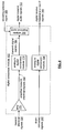
- FIG 3 is a schematic block diagram of an embodiment of the transmit acoustic transducer circuit 100 that includes a transducer 160 and a bias circuit 162.
- the biasing circuit 162 is coupled to the transducer 160 to provide a desired bias level for the transducer 160.
- the transducer 160 which may be a capacitive transducer, a Microelectromechanical Systems (MEMs) microphone, and/or a floating electrode capacitive microphone, converts the transmit sounds waves 118 into the transmit electrical signals 120 based on the biasing provided by the bias circuit 162.
- MEMs Microelectromechanical Systems
- Figure 4 is a schematic block diagram of an embodiment of the transmit acoustic transducer circuit 100 that includes a plurality of transducers 160-1 through 160-n and a biasing circuit 164.
- the plurality of transducers 160-1 through 160-n may be coupled in parallel, coupled in an array, or function separately.
- the bias circuit 164 provides a common biasing to the transducers such that the transducers may convert the transmit sounds waves 118 into the transmit electrical signals 120.
- the bias circuit 164 When the plurality of transducers 160-1 through 160-n are coupled in an array, the bias circuit 164 provides a common biasing or a biasing based on the structure of the array to the transducers such that the transducers may convert the transmit sounds waves 118 into the transmit electrical signals 120. When the plurality of transducers 160-1 through 160-n function separately, the bias circuit 164 provides separate biasing to the transducers such each of the transducers produces electrical signals from the transmit sounds waves 118 and the bias circuit combines the electrical signals to produce the transmit electrical signals 120. Note that the transducers 160-1 through 160-n may be capacitive transducers, Microelectromechanical Systems (MEMs) microphones, and/or floating electrode capacitive microphones.
- MEMs Microelectromechanical Systems
- FIG. 5 is a schematic block diagram of an embodiment of the receive acoustic transducer circuit 116 that includes a transducer 170 and a bias circuit 172.
- the biasing circuit 172 is coupled to the transducer 170 to provide a desired bias level for the transducer 170.
- the transducer 170 which may be a capacitive transducer, a Microelectromechanical Systems (MEMs) speaker, and/or a floating electrode capacitive speaker, converts the receive electrical signals 148 into the receive sounds waves 150 based on the biasing provided by the bias circuit 172.
- MEMs Microelectromechanical Systems
- Figure 6 is a schematic block diagram of an embodiment of the receive acoustic transducer circuit 116 that includes a plurality of transducers 170-1 through 170-n and a biasing circuit 174.
- the plurality of transducers 170-1 through 170-n may be coupled in parallel, coupled in an array, or function separately.
- the bias circuit 174 provides a common biasing to the transducers such that the transducers may convert the receive electrical signals 148 into the receive sounds waves 150.
- the bias circuit 174 provides a common biasing or a biasing based on the structure of the array to the transducers such that the transducers may convert the receive electrical signals 148 into the receive sounds waves 150.
- the bias circuit 174 provides separate biasing to the transducers such each of the transducers produces sound waves from the receive electrical signals 148 as provided by the biasing circuit 174.
- the transducers 170-1 through 170-n may be capacitive transducers, Microelectromechanical Systems (MEMs) speakers, and/or floating electrode capacitive speakers.
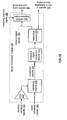
- Figure 7 is a schematic block diagram of an embodiment of the digital conversion module 102 that includes a multiplexer 176, an amplifier 170, an analog to digital conversion module 174, a multiplexer 178, and an audio encoding module 180.
- the multiplexers 176 and 178 which may be switches, gates, connection nodes, and/or multiplexers, are controlled by the status of the transmit/receive mode signal 124. Note that when the RFIC is in a half duplex mode, the transmit/receive mode signal 124 may be inherent in the RFIC based on whether the transmit path is active or the receive path is active. In this instance, the multiplexers 176 and 178 may be implemented as the connection nodes (i.e., electrically connection with one line active and the other inactive in accordance with the RFIC half duplex operation).
- multiplexer 176 When the RFIC is in the transmit mode, multiplexer 176 provides the transmit electrical signals 120 to the amplifier 170.
- the amplifier 170 amplifies the transmit electrical signals 120 in accordance with a pre-established gain setting or an automatic gain control setting to produce amplified transmit electric signals 182.
- the analog to digital conversion module 174 which may include one or more analog to digital converters, is coupled to convert the amplified transmit electrical signals 182 into transmit digital signals 184.
- Multiplexer 178 provides the transmit digital signals 184 to the audio encoding module 180.
- the audio encoding module 180 may be a separate processing device from the transmit baseband processing module 104, may share a processing device with the transmit baseband processing module 104, or may be a module within the transmit baseband processing module 104. Regardless of the specific implementation, the audio encoding module 180 perform one or more types of audio encoding upon the transmit digital signals 184 to produce the digital transmit audio signals 122. Such encoding includes A-law pulse code modulation, ⁇ -law pulse code modulation, and/or continuous variable slope delta modulation. In one embodiment, the audio encoding module 180 includes an input for receiving an audio encoding selection signal 188 which indicates the particular type of audio encoding it is to perform.
- the multiplexer 176 When the RFIC is in the receive mode, the multiplexer 176 provides the down-converted signals 142 to the amplifier 170.
- the amplifier 170 amplifies the down-converted signals 142 in accordance with an automatic gain control setting to produce amplified down-converted signals 186. Note that if the down-converted signals 142 include in-phase components and quadrature components, the amplifier 170 includes an in-phase amplifier to amplify the in-phase components and a quadrature amplifier to amplify the quadrature components.
- the analog to digital conversion module 174 converts the amplified down-converted signals 186 into the digital receive baseband or low IF signals 144. Note that when the down-converted signals 142 include in-phase components and quadrature components, the analog to digital conversion module 174 includes an in-phase analog to digital converter to convert the in-phase components and a quadrature analog to digital converter to convert the quadrature components. Multiplexer 178 provides the digital receive baseband or low IF signals 142 to the receive baseband processing module 116.
- Figure 8 is a schematic block diagram of an embodiment of the digital conversion module 102 that includes an amplifier 170, an analog to digital conversion (ADC) module 174, a an analog to digital conversion module 194, and the audio encoding module 180.
- ADC analog to digital conversion
- FIG. 8 when the RFIC is in the transmit mode, the amplifier 170, ADC module 174, and the audio encoding module 180 are active, while the ADC module 194 is inactive and when the RFIC is in the receive mode, the amplifier 170, ADC module 174, and the audio encoding module 180 are inactive, while the ADC module 194 is active.
- the amplifier 170 When the RFIC is in the transmit mode, the amplifier 170 amplifies the transmit electrical signals 120 in accordance with a pre-established gain setting or an automatic gain control setting to produce amplified transmit electric signals 182.
- the analog to digital conversion module 174 which may include one or more analog to digital converters, is coupled to convert the amplified transmit electrical signals 182 into transmit digital signals 184.
- the audio encoding module 180 perform one or more types of audio encoding upon the transmit digital signals 184 to produce the digital transmit audio signals 122. Such encoding includes A-law pulse code modulation, ⁇ -law pulse code modulation, and/or continuous variable slope delta modulation.
- the audio encoding module 180 includes an input for receiving an audio encoding selection signal 188 which indicates the particular type of audio encoding it is to perform.
- the analog to digital conversion module 194 converts the down-converted signals 142 into the digital receive baseband or low IF signals 144. Note that when the down-converted signals 142 include in-phase components and quadrature components, the analog to digital conversion module 194 includes an in-phase analog to digital converter to convert the in-phase components and a quadrature analog to digital converter to convert the quadrature components.
- Figure 9 is a schematic block diagram of an embodiment of the digital conversion module 102 that includes amplifier 170, the analog to digital conversion module 174, the audio encoding module 180, the analog to digital conversion module 194, amplifier 190 or digital amplifier 196.
- the amplifier 170, ADC module 174, and the audio encoding module 180 are active, while the ADC module 194 and the amplifier 190 or digital amplifier 196 are inactive and when the RFIC is in the receive mode, the amplifier 170, ADC module 174, and the audio encoding module 180 are inactive, while the ADC module 194 and the amplifier 190 or digital amplifier 196 are active.
- the amplifier 170 When the RFIC is in the transmit mode, the amplifier 170 amplifies the transmit electrical signals 120 in accordance with a pre-established gain setting or an automatic gain control setting to produce amplified transmit electric signals 182.
- the analog to digital conversion module 174 which may include one or more analog to digital converters, is coupled to convert the amplified transmit electrical signals 182 into transmit digital signals 184.
- the audio encoding module 180 perform one or more types of audio encoding upon the transmit digital signals 184 to produce the digital transmit audio signals 122. Such encoding includes A-law pulse code modulation, ⁇ -law pulse code modulation, and/or continuous variable slope delta modulation.
- the audio encoding module 180 includes an input for receiving an audio encoding selection signal 188 which indicates the particular type of audio encoding it is to perform.
- the amplifier 190 amplifies the down-converted signals 142 to produce amplified down-converted signals 186.
- the analog to digital conversion module 194 converts the amplified down-converted signals 186 into the digital receive baseband or low IF signals 144. Note that when the down-converted signals 142 include in-phase components and quadrature components, the analog to digital conversion module 194 includes an in-phase analog to digital converter to convert the in-phase components and a quadrature analog to digital converter to convert the quadrature components. In an alternative embodiment, the analog to digital conversion module 194 converts the amplified down-converted signals 186 into pre-amplified digital receive baseband or low IF signals.
- the digital amplifier 196 amplifies the pre-amplified digital receive baseband or low IF signals to produce the digital receive baseband or low IF signals 144.
- Figure 10 is a schematic block diagram of an embodiment of the digital conversion module 102 that includes amplifier 170, a combining module 200, the analog to digital conversion module 174, a separation module 202, and the audio encoding module 180.
- the RFIC is in a full duplex mode (i.e., simultaneously in the receive mode and transmit mode) where the transmit path uses a different frequency range than the receive path.
- the amplifier 170 amplifies the transmit electrical signals 120 based on a pre-determined gain setting and/or an automatic gain control setting to produce amplified transmit electrical signals 120.
- the combining module 200 combines the amplified transmit electrical signals with the down-converted signals 142 to produce combined signals 204.
- the combining module 200 may combine the amplified transmit electrical signals with the in-phase components and/or the quadrature components.
- the analog to digital conversion module 174 converts the combined signals 204 into digital combined signals.
- the separation module 202 separates the digital combined signals into the transmit digital signals 184 and the digital receive baseband or low IF signals 144.
- the separation module 200 may include a first digital filter and a second digital filter. The first digital filter is tuned to pass the cos 2 ⁇ t component of the combined signals 204 while substantially attenuating the sin 2 ⁇ IF t component of the combined signals 204 and the second digital filter is tuned to pass the sin 2 ⁇ IF t component of the combined signals 204 while substantially attenuating the cos 2 ⁇ t component of the combined signals 204.
- the separation module 200 may further include a digital square root function to obtain cos ⁇ t and sin ⁇ IF t and may further include a digital 90° phase shift module to phase shift sin ⁇ IF t to obtain cos ⁇ IF t.
- the audio encoding module 180 perform one or more types of audio encoding upon the transmit digital signals 184 to produce the digital transmit audio signals 122.
- Such encoding includes A-law pulse code modulation, ⁇ -law pulse code modulation, and/or continuous variable slope delta modulation.
- the audio encoding module 180 includes an input for receiving an audio encoding selection signal 188 which indicates the particular type of audio encoding it is to perform.
- FIG 11 is a schematic block diagram of an embodiment of the analog conversion module 106 that includes an audio decoding module 210, a multiplexer 216, a digital to analog conversion module 212, a multiplexer 218, and an amplifier 214.
- the multiplexers 216 and 218, which may be switches, gates, connection nodes, and/or multiplexers, are controlled by the status of the transmit/receive mode signal 124. Note that when the RFIC is in a half duplex mode, the transmit/receive mode signal 124 may be inherent in the RFIC based on whether the transmit path is active or the receive path is active. In this instance, the multiplexers 216 and 218 may be implemented as the connection nodes (i.e., electrically connection with one line active and the other inactive in accordance with the RFIC half duplex operation).
- the audio decoding module 210 decodes the digital receive audio signals 146 in accordance with an audio decoding scheme, which may be A-law pulse code demodulation, ⁇ -law pulse code demodulation, and continuous variable slope delta demodulation.
- the audio decoding module 210 may include an input for receiving an audio decoding selection signal 212 that indicates the particular type of audio decoding to be performed.
- the audio decoding module 210 may be a separate processing device from the receive baseband processing module 116, may share a processing device with the receive baseband processing module 116, or may be a module within the receive baseband processing module 116.
- multiplexer 216 provides the decoded receive audio signals from the audio decoding module 210 to the digital to analog conversion (DAC) module 212.
- the DAC module 212 may include one or more digital to analog converts to convert the decoded receive audio signals into analog decoded audio signals.
- the amplifier 214 amplifies the analog decoded audio signals in accordance with a pre-determined gain setting and/or an automatic gain control setting to produce the receive electrical signals 148.
- multiplexer 216 When the RFIC is in the transmit mode, multiplexer 216 provides the digital transmit baseband or low IF signals 126 to the DAC module 212.
- the transmit baseband or low IF signals 126 may include in-phase components and quadrature components.
- the DAC module 212 would include two digital to analog converters: one for the in-phase components and another for the quadrature components.
- multiplexer 218 provides the analog transmit baseband or low IF signals 128 to the up-conversion module 106. Note that the analog transmit baseband or low IF signals 128 may be amplified and/or filtered prior to or after multiplexer 218.
- Figure 12 is a schematic block diagram of an embodiment of the analog conversion module 106 that includes an audio decoding module 210, a multiplexer 216, a digital to analog conversion module 212, a multiplexer 218, and an amplifier 214.
- This embodiment is similar to the embodiment of Figure 11 with the exception that amplifier 214 is coupled to the DAC module 212 and the output of the amplifier 214 provides the input to the multiplexer 218.
- Figure 13 is a schematic block diagram of an embodiment of the analog conversion module 106 that includes the audio decoding module 210, the DAC module 212, the amplifier 214, and a second DAC module 222.
- the audio decoding module 210, the DAC module 212, and the amplifier 214 are active, while the DAC module 222 is inactive and when the RFIC is in the receive mode, audio decoding module 210, the DAC module 212, and the amplifier 214 are inactive, while the DAC module 222 is active.
- the audio decoding module 210 decodes the digital receive audio signals 146 in accordance with an audio decoding scheme, which may be A-law pulse code demodulation, ⁇ -law pulse code demodulation, and continuous variable slope delta demodulation.
- the audio decoding module 210 may include an input for receiving an audio decoding selection signal 212 that indicates the particular type of audio decoding to be performed.
- the DAC module 212 may include one or more digital to analog converts to convert the decoded receive audio signals into analog decoded audio signals.
- the amplifier 214 amplifies the analog decoded audio signals in accordance with a pre-determined gain setting and/or an automatic gain control setting to produce the receive electrical signals 148.
- the DAC module 222 converts the digital transmit baseband or low IF signals 126 into analog transmit baseband or low IF signals 128.
- the transmit baseband or low IF signals 126 may include in-phase components and quadrature components.
- the DAC module 222 would include two digital to analog converters: one for the in-phase components and another for the quadrature components.
- Figure 14 is a schematic block diagram of an embodiment of the analog conversion module 106 that includes the audio decoding module 210, the DAC module 212, the amplifier 214, the second DAC module 222, an amplifier 224 or a digital amplifier 226.
- the audio decoding module 210, the DAC module 212, and the amplifier 214 are active, while the DAC module 222, the amplifier 224, and the digital amplifier 226 are inactive and when the RFIC is in the receive mode, audio decoding module 210, the DAC module 212, and the amplifier 214 are inactive, while the DAC module 222, the amplifier 224, and the digital amplifier 226 are active.
- the audio decoding module 210 decodes the digital receive audio signals 146 in accordance with an audio decoding scheme, which may be A-law pulse code demodulation, ⁇ -law pulse code demodulation, and continuous variable slope delta demodulation.
- the audio decoding module 210 may include an input for receiving an audio decoding selection signal 212 that indicates the particular type of audio decoding to be performed.
- the DAC module 212 may include one or more digital to analog converts to convert the decoded receive audio signals into analog decoded audio signals.
- the amplifier 214 amplifies the analog decoded audio signals in accordance with a pre-determined gain setting and/or an automatic gain control setting to produce the receive electrical signals 148.
- the DAC module 222 converts the digital transmit baseband or low IF signals 126 into pre-amplified analog transmit baseband or low IF signals.
- the amplifier 224 amplifies the pre-amplified analog transmit baseband or low IF signals to produce the analog transmit baseband or low IF signals 128.
- the digital amplifier 226 amplifies the digital transmit baseband or low IF signals 126 prior to the DAC module 222 converting the signals into the analog transmit baseband or low IF signals 128.
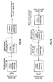
- FIG 15 is a schematic block diagram of a radio transmitter integrated circuit that includes the transmit acoustic transducer circuit 100, a digital conversion module 240, and the transmit baseband processing module 104.
- the transmit acoustic transducer circuit 100 converts transmit sound waves 118 into transmit electrical signals 120.
- the digital conversion module 240 which may be implemented via amplifier 170, analog to digital conversion module 174, and audio encoding module of Figures 8 and 9, converts the transmit electrical signals 120 into the digital transmit audio signals 240.
- the transmit baseband processing module 104 converts the digital transmit audio signals 122 into the digital transmit baseband or low IF signals 126.
- the radio transmitter integrated circuit may further include an analog conversion module, which may include DAC module 222 of Figures 13 and 14, an up-conversion module 108, and/or a power amplifier circuit 110. Further note that the analog conversion module may include amplifier 224 and/or digital amplifier 226 of Figure 14.
- Figure 16 is a schematic block diagram of a radio receiver integrated circuit that includes a digital conversion module 248, the receive baseband processing module 115, an analog conversion module 244, and the receive acoustic transducer circuit 116.
- the digital conversion module 248, which may be implemented via the ADC module 194 of Figures 8 and 9, converts the down-converted signals 142 into the digital receive baseband or low IF signals 144.
- the digital conversion module 248 may further include amplifier 190 and/or digital amplifier 196.
- the receive baseband processing module 115 convert the digital receive baseband or low IF signals 144 into the digital receive audio signals 146.
- the analog conversion module 244 which may be implemented via audio decoding module 210, DAC module 212, and amplifier 214 of Figures 13 and 14, converts the digital receive audio signals 146 into the receive electrical signals 148.
- the receive acoustic transducer circuit 116 converts the receive electrical signals 148 into receive sound waves 150.
- the radio receiver integrated circuit may further include the down-conversion module 114 and the low noise amplifier circuit 112.
- the terms “substantially” and “approximately” provides an industry-accepted tolerance for its corresponding term and/or relativity between items. Such an industry-accepted tolerance ranges from less than one percent to fifty percent and corresponds to, but is not limited to, component values, integrated circuit process variations, temperature variations, rise and fall times, and/or thermal noise. Such relativity between items ranges from a difference of a few percent to magnitude differences.
- the term(s) "coupled to” and/or “coupling” and/or includes direct coupling between items and/or indirect coupling between items via an intervening item (e.g., an item includes, but is not limited to, a component, an element, a circuit, and/or a module) where, for indirect coupling, the intervening item does not modify the information of a signal but may adjust its current level, voltage level, and/or power level.
- an intervening item e.g., an item includes, but is not limited to, a component, an element, a circuit, and/or a module
- inferred coupling i.e., where one element is coupled to another element by inference
- the term "operable to” indicates that an item includes one or more of power connections, input(s), output(s), etc., to perform one or more its corresponding functions and may further include inferred coupling to one or more other items.
- the term “associated with”, includes direct and/or indirect coupling of separate items and/or one item being embedded within another item.
- the term “compares favorably”, indicates that a comparison between two or more items, signals, etc., provides a desired relationship. For example, when the desired relationship is that signal 1 has a greater magnitude than signal 2, a favorable comparison may be achieved when the magnitude of signal 1 is greater than that of signal 2 or when the magnitude of signal 2 is less than that of signal 1.
Landscapes
- Engineering & Computer Science (AREA)
- Computer Networks & Wireless Communication (AREA)
- Signal Processing (AREA)
- Transceivers (AREA)
- Amplifiers (AREA)
Abstract
Description
- This invention relates generally to wireless communication systems and more particularly to wireless communication devices.
- Communication systems are known to support wireless and wire lined communications between wireless and/or wire lined communication devices. Such communication systems range from national and/or international cellular telephone systems to the Internet to point-to-point in-home wireless networks. Each type of communication system is constructed, and hence operates, in accordance with one or more communication standards. For instance, wireless communication systems may operate in accordance with one or more standards including, but not limited to, IEEE 802.11, Bluetooth, ZigBee, advanced mobile phone services (AMPS), digital AMPS, global system for mobile communications (GSM), code division multiple access (CDMA), local multi-point distribution systems (LMDS), multi-channel-multi-point distribution systems (MMDS), radio frequency identification (RFID), and/or variations thereof.
- Depending on the type of wireless communication system, a wireless communication device, such as a cellular telephone, two-way radio, personal digital assistant (PDA), personal computer (PC), laptop computer, home entertainment equipment, RFID reader, RFID tag, et cetera communicates directly or indirectly with other wireless communication devices. For direct communications (also known as point-to-point communications), the participating wireless communication devices tune their receivers and transmitters to the same channel or channels (e.g., one of the plurality of radio frequency (RF) carriers of the wireless communication system or a particular RF frequency for some systems) and communicate over that channel(s). For indirect wireless communications, each wireless communication device communicates directly with an associated base station (e.g., for cellular services) and/or an associated access point (e.g., for an in-home or in-building wireless network) via an assigned channel. To complete a communication connection between the wireless communication devices, the associated base stations and/or associated access points communicate with each other directly, via a system controller, via the public switch telephone network, via the Internet, and/or via some other wide area network.
- For each wireless communication device to participate in wireless communications, it includes a built-in radio transceiver (i.e., receiver and transmitter) or is coupled to an associated radio transceiver (e.g., a station for in-home and/or in-building wireless communication networks, RF modem, etc.). As is known, the receiver is coupled to the antenna and includes a low noise amplifier, one or more intermediate frequency stages, a filtering stage, and a data recovery stage. The low noise amplifier receives inbound RF signals via the antenna and amplifies then. The one or more intermediate frequency stages mix the amplified RF signals with one or more local oscillations to convert the amplified RF signal into baseband signals or intermediate frequency (IF) signals. The filtering stage filters the baseband signals or the IF signals to attenuate unwanted out of band signals to produce filtered signals. The data recovery stage recovers raw data from the filtered signals in accordance with the particular wireless communication standard.
- As is also known, the transmitter includes a data modulation stage, one or more intermediate frequency stages, and a power amplifier. The data modulation stage converts raw data into baseband signals in accordance with a particular wireless communication standard. The one or more intermediate frequency stages mix the baseband signals with one or more local oscillations to produce RF signals. The power amplifier amplifies the RF signals prior to transmission via an antenna.
- In many applications of a radio transceiver, the raw data that is transmitted and/or received includes digitized audio signals (e.g., digitized voice, music files such as MP3 files, video files such as MPEG files, and/or a combination thereof). As is known, a microphone is used to capture analog audio signals and a speaker is used to render analog audio signals audible. As is known, analog audio signals captured by a microphone are biased to a particular level, amplified, and digitized (i.e., converted to digital signals and may further be encoded in accordance with an encoding format). As is further known, digitized audio signals are converted to analog audio signals, amplified via a volume control, and subsequently rendered audible by a speaker.
- Recently, through the advent of Microelectromechanical Systems (MEMs), a few companies have developed microphone integrated circuits and speaker integrated circuits. For example, Akustica, as claimed on its web page (Akustica.com), has developed an analog microphone chip (part no. AKU1000), a digital microphone chip (part no. AKU2000), and speaker chips. While integrated microphone chips and speaker chips offer communication device manufacturers smaller form factors, the chips are still separate components requiring printed circuit board (PCB) space and connections to and/or from other integrated circuits on the PCB.
- Therefore, a need exists for a radio frequency integrated circuit that includes an on-chip acoustic transducer circuit.
- The present invention is directed to apparatus and methods of operation that are further described in the following Brief Description of the Drawings, the Detailed Description of the Invention, and the claims.
- According to an aspect of the invention, a radio frequency integrated circuit (RFIC) comprises:
- a transmit acoustic transducer circuit coupled to convert transmit sound waves into transmit electrical signals;
- a digital conversion module coupled to convert the transmit electrical signals into digital transmit audio signals when the RFIC is in a transmit mode and to convert down-converted signals into digital receive baseband or low intermediate frequency (IF) signals when the RFIC is in a receive mode;
- a transmit baseband processing module coupled to convert the digital transmit audio signals into digital transmit baseband or low IF signals;
- an analog conversion module coupled to convert the digital transmit baseband or low IF signals into analog transmit baseband or low IF signals when the RFIC is in the transmit mode and to convert digital receive audio signals into receive electrical signals when the RFIC is in the receive mode;
- an up-conversion module coupled to convert the analog transmit baseband or low IF signals into up-converted signals based on a transmit local oscillation;
- a power amplifier circuit coupled to amplify the up-converted signals to produce transmit radio frequency (RF) signals;
- a low noise amplifier circuit coupled to amplify receive RF signals to produce amplified receive RF signals;
- a down-conversion module coupled to convert the amplified receive RF signals into the down-converted signals based on a receive local oscillation;
- a receive baseband processing module coupled to convert the digital receive baseband or low IF signals into the digital receive audio signals; and
- a receive acoustic transducer circuit coupled to convert the receive electrical signals into receive sound waves.
- Advantageously, the transmit acoustic transducer circuit comprises:
- a transducer; and
- a bias circuit coupled to the transducer, wherein the transducer converts, based on biasing provided by the bias circuit, the transmit sounds waves into the transmit electrical signals.
- Advantageously, the transducer comprises at least one of:
- a capacitive transducer;
- a Microelectromechanical Systems (MEMs) microphone;
- a floating electrode capacitive microphone.
- Advantageously, the transmit acoustic transducer circuit comprises:
- a plurality of transducers; and
- a bias circuit coupled to the plurality of transducers, wherein the plurality of transducers converts, based on biasing provided by the bias circuit, the transmit sounds waves into the transmit electrical signals.
- Advantageously, the receive acoustic transducer circuit comprises:
- a transducer; and
- a bias circuit coupled to the transducer, wherein the transducer converts, based on biasing provided by the bias circuit, the receive electrical signals into the receive sounds waves.
- Advantageously, the transducer comprises at least one of:
- a capacitive transducer;
- a Microelectromechanical Systems (MEMs) speaker;
- a floating electrode capacitive speaker.
- Advantageously, the receive acoustic transducer circuit comprises:
- a plurality of transducers; and
- a bias circuit coupled to the plurality of transducers, wherein the plurality of transducers converts, based on biasing provided by the bias circuit, the receive electrical signals into the receive sounds waves.
- Advantageously, the digital conversion module comprises:
- an amplifier coupled to amplify the transmit electrical signals to produce amplified transmit electrical signals when the RFIC is in the transmit mode and to amplify the down-converted signals to produce amplified down-converted signals when the RFIC is in the receive mode;
- an analog to digital conversion module coupled to convert the amplified transmit electrical signals into transmit digital signals when the RFIC is in the transmit mode and to convert the amplified down-converted signals into the digital receive baseband or low IF signals when the RFIC is in the receive mode; and
- an audio encoding module coupled to convert the transmit digital signals into the digital transmit audio signals.
- Advantageously, audio encoding module comprises:
- an input for receiving an audio encoding selection signal, wherein the audio encoding selection signal indicates at least one of: A-law pulse code modulation, µ-law pulse code modulation, and continuous variable slope delta modulation.
- Advantageously, the digital conversion module comprises:
- an amplifier coupled to amplify the transmit electrical signals to produce amplified transmit electrical signals when the RFIC is in the transmit mode;
- a first analog to digital conversion module coupled to convert the amplified transmit electrical signals into transmit digital signals when the RFIC is in the transmit mode;
- a second analog to digital conversion module coupled to convert the down-converted signals into the digital receive baseband or low IF signals when the RFIC is in the receive mode; and
- an audio encoding module coupled to convert the transmit digital signals into the digital transmit audio signals.
- Advantageously, the digital conversion module further comprises:
- a second amplifier coupled to amplify the down-converted signals to produce prior to the second analog to digital conversion module converting the down-converted signals into the digital receive baseband or low IF signals.
- Advantageously, the digital conversion module further comprises:
- a digital amplifier coupled to amplify the digital receive baseband or low IF signals.
- Advantageously, the digital conversion module comprises:
- an amplifier coupled to amplify the transmit electrical signals to produce amplified transmit electrical signals;
- a combining module coupled to combine the amplified transmit electrical signals with the down-converted signals to produce combined signals;
- an analog to digital conversion module coupled to convert the combined signals into digital combined signals;
- a separation module coupled to separate the digital combined signals into transmit digital signals and digital receive baseband or low IF signals; and
- an audio encoding module coupled to convert the transmit digital signals into the digital transmit audio signals, wherein the transmit RF signals are within a transmit frequency band and the receive RF signals are within a receive frequency band such that the RFIC is simultaneously in the transmit mode and the receive mode.
- Advantageously, the analog conversion module comprises:
- an audio decoding module coupled to convert the digital receive audio signals into receive digital signals;
- a digital to analog conversion module coupled to convert the receive digital signals into pre-amplified receive electrical signals when the RFIC is in the receive mode and to convert the digital transmit baseband or low IF signals into the analog transmit baseband or low IF signals when the RFIC is in the transmit mode; and
- an amplifier coupled to amplified the pre-amplified receive electrical signals to produce the receive electrical signals when the RFIC is in the receive mode.
- Advantageously, the amplifier is further coupled to:
- amplify the analog transmit baseband or low IF signals when the RFIC is in the transmit mode.
- Advantageously, audio decoding module comprises:
- an input for receiving an audio decoding selection signal, wherein the audio decoding selection signal indicates at least one of: A-law pulse code demodulation, µ-law pulse code demodulation, and continuous variable slope delta demodulation.
- Advantageously, the analog conversion module comprises:
- an audio decoding module coupled to convert the digital receive audio signals into receive digital signals;
- a first digital to analog conversion module coupled to convert the receive digital signals into pre-amplified receive electrical signals when the RFIC is in the receive mode;
- a second digital to analog conversion module coupled to convert the digital transmit baseband or low IF signals into the analog transmit baseband or low IF signals when the RFIC is in the transmit mode; and
- an amplifier coupled to amplified the pre-amplified receive electrical signals to produce the receive electrical signals when the RFIC is in the receive mode.
- Advantageously, the analog conversion module further comprises:
- a second amplifier coupled to amplify the analog transmit baseband or low IF signals.
- Advantageously, the analog conversion module further comprises:
- a digital amplifier coupled to amplify the digital transmit baseband or low IF signals prior to the second digital to analog conversion module converting the digital transmit baseband or low IF signals into the analog transmit baseband or low IF signals.
- Advantageously, the RFIC further comprises:
- a first die that supports the transmit acoustic transducer circuit, the digital conversion module, the transmit baseband processing module, the analog conversion module, the receive baseband processing module, and the receive acoustic transducer circuit;
- a second die that supports the up-conversion module, the power amplifier circuit, the low noise amplifier circuit, and the down-conversion module; and
- a package that supports the first and second dies.
- According to an aspect of the invention, a radio transmitter integrated circuit (RTIC) comprises:
- a transmit acoustic transducer circuit coupled to convert transmit sound waves into transmit electrical signals;
- a digital conversion module coupled to convert the transmit electrical signals into digital transmit audio signals; and
- a transmit baseband processing module coupled to convert the digital transmit audio signals into digital transmit baseband or low IF signals.
- Advantageously, the RTIC further comprises:
- an analog conversion module coupled to convert the digital transmit baseband or low IF signals into analog transmit baseband or low IF signals;
- an up-conversion module coupled to convert the digital transmit baseband or low IF signals into up-converted signals based on a transmit local oscillation; and
- a power amplifier circuit coupled to amplify the up-converted signals to produce transmit radio frequency (RF) signals.
- Advantageously, the transmit acoustic transducer circuit comprises:
- a transducer; and
- a bias circuit coupled to the transducer, wherein the transducer converts, based on biasing provided by the bias circuit, the transmit sounds waves into the transmit electrical signals.
- Advantageously, the transmit acoustic transducer circuit comprises:
- a plurality of transducers; and
- a bias circuit coupled to the plurality of transducers, wherein the plurality of transducers converts, based on biasing provided by the bias circuit, the transmit sounds waves into the transmit electrical signals.
- Advantageously, the digital conversion module comprises:
- an amplifier coupled to amplify the transmit electrical signals to produce amplified transmit electrical signals;
- an analog to digital conversion module coupled to convert the amplified transmit electrical signals into transmit digital signals; and
- an audio encoding module coupled to convert the transmit digital signals into the digital transmit audio signals.
- Advantageously, audio encoding module comprises:
- an input for receiving an audio encoding selection signal, wherein the audio encoding selection signal indicates at least one of: A-law pulse code modulation, µ-law pulse code modulation, and continuous variable slope delta modulation.
- Advantageously, the analog conversion module comprises:
- a digital to analog conversion module coupled to convert the digital transmit baseband or low IF signals into the analog transmit baseband or low IF signals.
- Advantageously, the analog conversion module further comprises:
- an amplifier coupled to amplify the analog transmit baseband or low IF signals.
- According to an aspect of the invention, a radio receiver integrated circuit (RRIC) comprises:
- a digital conversion module coupled to convert down-converted signals into digital receive baseband or low intermediate frequency (IF) signals;
- a receive baseband processing module coupled to convert the digital receive baseband or low IF signals into the digital receive audio signals;
- an analog conversion module coupled to convert the digital receive audio signals into receive electrical signals; and
- a receive acoustic transducer circuit coupled to convert the receive electrical signals into receive sound waves.
- Advantageously, the RRIC further comprises:
- a low noise amplifier circuit coupled to amplify receive RF signals to produce amplified receive RF signals; and
- a down-conversion module coupled to convert the amplified receive RF signals into the down-converted signals based on a receive local oscillation.
- Advantageously, the receive acoustic transducer circuit comprises:
- a transducer; and
- a bias circuit coupled to the transducer, wherein the transducer converts, based on biasing provided by the bias circuit, the receive electrical signals into the receive sounds waves.
- Advantageously, the receive acoustic transducer circuit comprises:
- a plurality of transducers; and
- a bias circuit coupled to the plurality of transducers, wherein the plurality of transducers converts, based on biasing provided by the bias circuit, the receive electrical signals into the receive sounds waves.
- Advantageously, the digital conversion module comprises:
- an analog to digital conversion module coupled to convert the down-converted signals into the digital receive baseband or low IF signals.
- Advantageously, the digital conversion module further comprises:
- an amplifier coupled to amplify the down-converted signals prior to the analog to digital conversion module converting the down-converted signals into the digital receive baseband or low IF signals.
- Advantageously, the analog conversion module comprises:
- an audio decoding module coupled to convert the digital receive audio signals into receive digital signals;
- a digital to analog conversion module coupled to convert the receive digital signals into pre-amplified receive electrical signals; and
- an amplifier coupled to amplified the pre-amplified receive electrical signals to produce the receive electrical signals.
- Advantageously, audio decoding module comprises:
- an input for receiving an audio decoding selection signal, wherein the audio decoding selection signal indicates at least one of: A-law pulse code demodulation, µ-law pulse code demodulation, and continuous variable slope delta demodulation.
- Other features and advantages of the present invention will become apparent from the following detailed description of the invention made with reference to the accompanying drawings.
-
- Figure 1 is a schematic block diagram of a wireless communication system in accordance with the present invention;
- Figure 2 is a schematic block diagram of a radio transceiver in accordance with the present invention;
- Figures 3 and 4 are schematic block diagrams of various embodiments of a transmit acoustic transducer circuit in accordance with the present invention;
- Figures 5 and 6 are schematic block diagrams of various embodiments of a receive acoustic transducer circuit in accordance with the present invention;
- Figures 7 - 10 are schematic block diagrams of various embodiments of a digital conversion module in accordance with the present invention;
- Figures 11 - 14 are schematic block diagrams of various embodiments of an analog conversion module in accordance with the present invention;
- Figure 15 is a schematic block diagram of a radio transmitter integrated circuit in accordance with the present invention; and
- Figure 16 is a schematic block diagram of a radio receiver integrated circuit in accordance with the present invention.
- Figure 1 is a schematic block diagram illustrating a
communication system 10 that includes a plurality of base stations and/oraccess points network hardware component 34. Note that thenetwork hardware 34, which may be a router, switch, bridge, modem, system controller, et cetera provides a widearea network connection 42 for thecommunication system 10. Further note that the wireless communication devices 18-32 may belaptop host computers -
Wireless communication devices devices system 10 or to communicate outside of thesystem 10, thedevices access points - The base stations or
access points areas network hardware 34 via localarea network connections access point 12 16 with connectivity to other devices within thesystem 10 and provides connectivity to other networks via theWAN connection 42. To communicate with the wireless communication devices within itsBSS access point 12 wirelessly communicates withwireless communication devices access point 16 wirelessly communicates with wireless communication devices 26 - 32. Typically, the wireless communication devices register with a particular base station oraccess point communication system 10. - Typically, base stations are used for cellular telephone systems and like-type systems, while access points, or master transceivers, are used for in-home or in-building wireless networks (e.g., IEEE 802.11 and versions thereof, Bluetooth, RFID, and/or any other type of radio frequency based network protocol). Regardless of the particular type of communication system, each wireless communication device includes a built-in radio and/or is coupled to a radio. Note that one or more of the wireless communication devices may include an RFID reader and/or an RFID tag.
- Figure 2 is a schematic block diagram of a radio frequency integrated circuit (RFIC) that may be used in any of the wireless communication devices of figure 1 or as a radio frequency transceiver for any other RF application where audio signals are transmitted and/or received. The RFIC includes a transmit
acoustic transducer 100, adigital conversion module 102, a transmitbaseband module 104, ananalog conversion module 106, an up-conversion module 108, apower amplifier circuit 110, a low noise amplifier circuit 112, a down-conversion module 114, a receivebaseband processing module 115, and a receiveacoustic transducer circuit 118. - The transmit acoustic transducer circuit 100 (embodiments of which will be described in greater detail with reference to Figures 3 and 4) is coupled to convert transmit
sound waves 118 into transmitelectrical signals 120. The transmitsound waves 118, which may result from human speech and/or any other source that produces a wave transmitted through the air, cause mechanical vibrations within the transmitacoustic transducer circuit 100. The transmitacoustic transducer circuit 100 converts the mechanical vibrations into the transmitelectrical signals 120. - The digital conversion module 102 (embodiments of which will be described in greater detail with reference to Figures 7-10) is coupled to convert the transmit
electrical signals 120 into digital transmitaudio signals 122 when the RFIC is in a transmit mode. The digital transmitaudio signals 122 may be encoded in accordance with one or more encoding schemes, such as Pulse Code Modulation (PCM) A-law, PCM µ-law, and continuous variable slope delta demodulation. Note that the RFIC may be in the transmit mode via a transmit/receivemode signal 124, may be in the transmit mode in accordance with a half duplex scheme where the transmit path and receive path of the RFIC share a wireless communication resource (e.g., one or more RF channels, use the same RF carrier frequency, frequency hopping scheme, etc.), and/or may be in the transmit mode simultaneously with the receive mode when the RFIC supports a full duplex scheme where the transmit path utilizes a different wireless communication resource than the receive path. - The transmit
baseband processing module 104 is coupled to convert the digital transmitaudio signals 122 into digital transmit baseband or low intermediate frequency (IF) signals 126 in accordance with one or more wireless communication standards. To achieve the conversion to the digital transmit baseband or low IFsignals 126, the transmitbaseband processing module 104 may perform one or more transmitter functions upon the digital transmitaudio signals 122. The transmitter functions include, but are not limited to, scrambling, encoding, puncturing, mapping, modulation, and/or digital baseband to IF conversion. Note that the baseband or low IF TX signals 164 may be digital baseband signals (e.g., have a zero IF) or digital low IF signals, where the low IF typically will be in a frequency range of one hundred kilohertz to a few megahertz. Further note that the transmitbaseband processing module 104 and the receivebaseband processing module 115 may be implemented using a shared processing device, individual processing devices, or a plurality of processing devices and may further included associated memory. Such a processing device may be a microprocessor, microcontroller, digital signal processor, microcomputer, central processing unit, field programmable gate array, programmable logic device, state machine, logic circuitry, analog circuitry, digital circuitry, and/or any device that manipulates signals (analog and/or digital) based on operational instructions. The associated memory may be a single memory device or a plurality of memory devices. Such a memory device may be a read-only memory, random access memory, volatile memory, non-volatile memory, static memory, dynamic memory, flash memory, and/or any device that stores digital information. Note that when theprocessing module 104 and/or 116 implements one or more of its functions via a state machine, analog circuitry, digital circuitry, and/or logic circuitry, the memory storing the corresponding operational instructions is embedded with the circuitry comprising the state machine, analog circuitry, digital circuitry, and/or logic circuitry. - The analog conversion module 106 (embodiments of which will be described in greater detail with reference to Figures 11-14) is coupled to convert the digital transmit baseband or low IF
signals 126 into analog transmit baseband or low IFsignals 128 when the RFIC is in the transmit mode. - The up-
conversion module 108 is coupled to convert the analog transmit baseband or low IFsignals 128, which may include in-phase components and quadrature components, into up-convertedsignals 132 based on a transmitlocal oscillation 130. The up-conversion module 108 may be a direct conversion module where the transmitlocal oscillation 130 corresponds to the difference between the IF of the analog transmit baseband or low IFsignals 128 and the carrier frequency of the transmit RF signals 134. Alternatively, the up-conversion module 108 may be a superheterodyne module where the transmitlocal oscillation 130 includes two oscillations: one to convert the analog baseband or low IFsignals 128 into intermediate frequency signals and a second to convert the intermediate frequency signals into signals having the carrier frequency of the transmit RF signals 134. Note that when the analog transmit baseband or low IFsignals 128 includes in-phase components and quadrature components, the transmitlocal oscillation 130 includes an in-phase component and a quadrature component such that the quadrature component of the transmit local oscillation is mixed with the quadrature components of the analog transmit baseband or low IFsignals 128 and the in-phase component of the transmit local oscillation is mixed with the in-phase components of the analog transmit baseband or low IF signals 128. - The
power amplifier circuit 110 is coupled to amplify the up-converted signals to produce the transmit radio frequency (RF) signals 134. Thepower amplifier circuit 110 may include one or more power amplifiers and/or one or more pre-amplifiers coupled in series, in parallel or combination thereof. The amplification provided by thepower amplifier circuit 110 is dependent upon the desired transmit power and whether an off-chip power amplifier is used. Thepower amplifier circuit 110 provides the transmitRF signals 134 to an antenna structure for over-the-air transmission. - The antenna structure may include a separate antenna(s) for the receive path and the transmit path of the RFIC or the transmit and receive paths may share an antenna(s) via a transmit/receive switch and/or transformer balun. In another embodiment, the receive and transmit paths may share a diversity antenna structure. In another embodiment, the receive and transmit paths may each have its own diversity antenna structure. In another embodiment, the receive and transmit paths may share a multiple input multiple output (MIMO) antenna structure. Accordingly, the antenna structure coupled to, or integrated on, the RFIC will depend on the particular standard(s) to which the wireless transceiver is compliant.
- The low noise amplifier (LNA) circuit 112 is coupled to amplify receive
RF signals 136 to produce amplified receive RF signals 138. The LNA circuit 112 may include one or more amplifiers and/or one or more pre-amplifiers coupled in series, in parallel, or a combination thereof to amplify the receiveRF signals 136 based on a gain setting. The gain setting is at least partially dependent upon the signal strength of the receiveRF signals 136 and the desired operating range of the receive path. - The down-
conversion module 114 is coupled to convert the amplified receive RF signals 138 into the down-convertedsignals 142 based on a receivelocal oscillation 140. The down-conversion module 114 may be a direct conversion module where the receivelocal oscillation 140 corresponds to a difference between the IF of the down-converted signals 142 (e.g., a zero IF or a low IF of a few Mega Hertz or less) and the carrier frequency of the receive RF signals 136. Alternatively, the down-conversion module 114 may be a superheterodyne module where the receivelocal oscillation 140 includes two oscillations: one to convert the receiveRF signals 136 into intermediate frequency signals and a second to convert the intermediate frequency signals into the down-convertedsignals 142. Note that LNA circuit 112 may provide in-phase components and quadrature components of the amplified receive RF signals 138 to the down-conversion module 114. In this instance, the receivelocal oscillation 140 includes an in-phase component and a quadrature component such that the quadrature component of the receivelocal oscillation 140 is mixed with the quadrature components of the amplified receive RF signals 138 and the in-phase component of the receivelocal oscillation 140 is mixed with the in-phase components of the amplified receive RF signals 138. - The
digital conversion module 102 converts the down-convertedsignals 142 into digital receive baseband or low intermediate frequency (IF) signals 144 when the RFIC is in a receive mode. Note that the RFIC may be in the receive mode via a transmit/receivemode signal 124, may be in the receive mode in accordance with a half duplex scheme where the transmit path and receive path of the RFIC share a wireless communication resource (e.g., one or more RF channels, use the same RF carrier frequency, frequency hopping scheme, etc.), and/or may be in the receive mode simultaneously with the transmit mode when the RFIC supports a full duplex scheme where the transmit path utilizes a different wireless communication resource than the receive path. - The receive
baseband processing module 115 is coupled to convert the digital receive baseband or low IFsignals 144 into the digital receiveaudio signals 146. To achieve the conversion to the digital receiveaudio signals 146, the receivebaseband processing module 115 may perform one or more receiver functions upon the digital receive baseband or low IF signals 144. The receiver functions include, but are not limited to, digital intermediate frequency to baseband conversion, demodulation, demapping, depuncturing, decoding, and/or descrambling. Note that the digital receive baseband or low IF signals 144may be digital baseband signals (e.g., have a zero IF) or digital low IF signals, where the low IF typically will be in a frequency range of one hundred kilohertz to a few megahertz. - The
analog conversion module 106 converts the digital receiveaudio signals 146 into receiveelectrical signals 148 when the RFIC is in the receive mode. Such a conversion may include decoding using one or more decoding schemes, which may include Pulse Code Modulation (PCM) A-law, PCM µ-law, and continuous variable slope delta demodulation. - The receive acoustic transducer circuit 116 (embodiments of which will be described in greater detail with reference to Figures 3 and 4) is coupled to convert the receive
electrical signals 148 into receivesound waves 150. The receivesound waves 150 are the result of mechanical vibrations within the receiveacoustic transducer circuit 116 in response to the receiveelectrical signals 148. - As one of ordinary skill in the art will appreciate, the RFIC may be fabricated on a single die and placed within a conventional integrated circuit (IC) package (e.g., ball grid array, surface mount, etc.). Alternatively, the RFIC may be fabricated on two dies that are placed within a single conventional IC package. For instance, a first die may support the transmit
acoustic transducer circuit 100, thedigital conversion module 102, the transmitbaseband processing module 104, theanalog conversion module 106, the receivebaseband processing module 115, and the receiveacoustic transducer circuit 116 and a second die that supports the up-conversion module 108, thepower amplifier circuit 110, the low noise amplifier circuit 112, and the down-conversion module 114. As another alternative, the RFIC may be fabricated on two dies that are placed in separate conventional IC package. - Figure 3 is a schematic block diagram of an embodiment of the transmit
acoustic transducer circuit 100 that includes atransducer 160 and abias circuit 162. The biasingcircuit 162 is coupled to thetransducer 160 to provide a desired bias level for thetransducer 160. Thetransducer 160, which may be a capacitive transducer, a Microelectromechanical Systems (MEMs) microphone, and/or a floating electrode capacitive microphone, converts the transmitsounds waves 118 into the transmitelectrical signals 120 based on the biasing provided by thebias circuit 162. - Figure 4 is a schematic block diagram of an embodiment of the transmit
acoustic transducer circuit 100 that includes a plurality of transducers 160-1 through 160-n and abiasing circuit 164. The plurality of transducers 160-1 through 160-n may be coupled in parallel, coupled in an array, or function separately. When the plurality of transducers 160-1 through 160-n are coupled in parallel, thebias circuit 164 provides a common biasing to the transducers such that the transducers may convert the transmitsounds waves 118 into the transmitelectrical signals 120. When the plurality of transducers 160-1 through 160-n are coupled in an array, thebias circuit 164 provides a common biasing or a biasing based on the structure of the array to the transducers such that the transducers may convert the transmitsounds waves 118 into the transmitelectrical signals 120. When the plurality of transducers 160-1 through 160-n function separately, thebias circuit 164 provides separate biasing to the transducers such each of the transducers produces electrical signals from the transmitsounds waves 118 and the bias circuit combines the electrical signals to produce the transmitelectrical signals 120. Note that the transducers 160-1 through 160-n may be capacitive transducers, Microelectromechanical Systems (MEMs) microphones, and/or floating electrode capacitive microphones. - Figure 5 is a schematic block diagram of an embodiment of the receive
acoustic transducer circuit 116 that includes atransducer 170 and abias circuit 172. The biasingcircuit 172 is coupled to thetransducer 170 to provide a desired bias level for thetransducer 170. Thetransducer 170, which may be a capacitive transducer, a Microelectromechanical Systems (MEMs) speaker, and/or a floating electrode capacitive speaker, converts the receiveelectrical signals 148 into the receivesounds waves 150 based on the biasing provided by thebias circuit 172. - Figure 6 is a schematic block diagram of an embodiment of the receive
acoustic transducer circuit 116 that includes a plurality of transducers 170-1 through 170-n and abiasing circuit 174. The plurality of transducers 170-1 through 170-n may be coupled in parallel, coupled in an array, or function separately. When the plurality of transducers 170-1 through 170-n are coupled in parallel, thebias circuit 174 provides a common biasing to the transducers such that the transducers may convert the receiveelectrical signals 148 into the receive sounds waves 150. When the plurality of transducers 170-1 through 170-n are coupled in an array, thebias circuit 174 provides a common biasing or a biasing based on the structure of the array to the transducers such that the transducers may convert the receiveelectrical signals 148 into the receive sounds waves 150. When the plurality of transducers 170-1 through 170-n function separately, thebias circuit 174 provides separate biasing to the transducers such each of the transducers produces sound waves from the receiveelectrical signals 148 as provided by the biasingcircuit 174. Note that the transducers 170-1 through 170-n may be capacitive transducers, Microelectromechanical Systems (MEMs) speakers, and/or floating electrode capacitive speakers. - Figure 7 is a schematic block diagram of an embodiment of the
digital conversion module 102 that includes a multiplexer 176, anamplifier 170, an analog todigital conversion module 174, a multiplexer 178, and anaudio encoding module 180. The multiplexers 176 and 178, which may be switches, gates, connection nodes, and/or multiplexers, are controlled by the status of the transmit/receivemode signal 124. Note that when the RFIC is in a half duplex mode, the transmit/receivemode signal 124 may be inherent in the RFIC based on whether the transmit path is active or the receive path is active. In this instance, the multiplexers 176 and 178 may be implemented as the connection nodes (i.e., electrically connection with one line active and the other inactive in accordance with the RFIC half duplex operation). - When the RFIC is in the transmit mode, multiplexer 176 provides the transmit
electrical signals 120 to theamplifier 170. Theamplifier 170 amplifies the transmitelectrical signals 120 in accordance with a pre-established gain setting or an automatic gain control setting to produce amplified transmitelectric signals 182. The analog todigital conversion module 174, which may include one or more analog to digital converters, is coupled to convert the amplified transmitelectrical signals 182 into transmitdigital signals 184. Multiplexer 178 provides the transmitdigital signals 184 to theaudio encoding module 180. - The
audio encoding module 180 may be a separate processing device from the transmitbaseband processing module 104, may share a processing device with the transmitbaseband processing module 104, or may be a module within the transmitbaseband processing module 104. Regardless of the specific implementation, theaudio encoding module 180 perform one or more types of audio encoding upon the transmitdigital signals 184 to produce the digital transmitaudio signals 122. Such encoding includes A-law pulse code modulation, µ-law pulse code modulation, and/or continuous variable slope delta modulation. In one embodiment, theaudio encoding module 180 includes an input for receiving an audioencoding selection signal 188 which indicates the particular type of audio encoding it is to perform. - When the RFIC is in the receive mode, the multiplexer 176 provides the down-converted
signals 142 to theamplifier 170. Theamplifier 170 amplifies the down-convertedsignals 142 in accordance with an automatic gain control setting to produce amplified down-convertedsignals 186. Note that if the down-convertedsignals 142 include in-phase components and quadrature components, theamplifier 170 includes an in-phase amplifier to amplify the in-phase components and a quadrature amplifier to amplify the quadrature components. - The analog to
digital conversion module 174 converts the amplified down-convertedsignals 186 into the digital receive baseband or low IF signals 144. Note that when the down-convertedsignals 142 include in-phase components and quadrature components, the analog todigital conversion module 174 includes an in-phase analog to digital converter to convert the in-phase components and a quadrature analog to digital converter to convert the quadrature components. Multiplexer 178 provides the digital receive baseband or low IFsignals 142 to the receivebaseband processing module 116. - Figure 8 is a schematic block diagram of an embodiment of the
digital conversion module 102 that includes anamplifier 170, an analog to digital conversion (ADC)module 174, a an analog todigital conversion module 194, and theaudio encoding module 180. In this embodiment, when the RFIC is in the transmit mode, theamplifier 170,ADC module 174, and theaudio encoding module 180 are active, while theADC module 194 is inactive and when the RFIC is in the receive mode, theamplifier 170,ADC module 174, and theaudio encoding module 180 are inactive, while theADC module 194 is active. - When the RFIC is in the transmit mode, the
amplifier 170 amplifies the transmitelectrical signals 120 in accordance with a pre-established gain setting or an automatic gain control setting to produce amplified transmitelectric signals 182. The analog todigital conversion module 174, which may include one or more analog to digital converters, is coupled to convert the amplified transmitelectrical signals 182 into transmitdigital signals 184. Theaudio encoding module 180 perform one or more types of audio encoding upon the transmitdigital signals 184 to produce the digital transmitaudio signals 122. Such encoding includes A-law pulse code modulation, µ-law pulse code modulation, and/or continuous variable slope delta modulation. In one embodiment, theaudio encoding module 180 includes an input for receiving an audioencoding selection signal 188 which indicates the particular type of audio encoding it is to perform. - When the RFIC is in the receive mode, the analog to
digital conversion module 194 converts the down-convertedsignals 142 into the digital receive baseband or low IF signals 144. Note that when the down-convertedsignals 142 include in-phase components and quadrature components, the analog todigital conversion module 194 includes an in-phase analog to digital converter to convert the in-phase components and a quadrature analog to digital converter to convert the quadrature components. - Figure 9 is a schematic block diagram of an embodiment of the
digital conversion module 102 that includesamplifier 170, the analog todigital conversion module 174, theaudio encoding module 180, the analog todigital conversion module 194,amplifier 190 ordigital amplifier 196. In this embodiment, when the RFIC is in the transmit mode, theamplifier 170,ADC module 174, and theaudio encoding module 180 are active, while theADC module 194 and theamplifier 190 ordigital amplifier 196 are inactive and when the RFIC is in the receive mode, theamplifier 170,ADC module 174, and theaudio encoding module 180 are inactive, while theADC module 194 and theamplifier 190 ordigital amplifier 196 are active. - When the RFIC is in the transmit mode, the
amplifier 170 amplifies the transmitelectrical signals 120 in accordance with a pre-established gain setting or an automatic gain control setting to produce amplified transmitelectric signals 182. The analog todigital conversion module 174, which may include one or more analog to digital converters, is coupled to convert the amplified transmitelectrical signals 182 into transmitdigital signals 184. Theaudio encoding module 180 perform one or more types of audio encoding upon the transmitdigital signals 184 to produce the digital transmitaudio signals 122. Such encoding includes A-law pulse code modulation, µ-law pulse code modulation, and/or continuous variable slope delta modulation. In one embodiment, theaudio encoding module 180 includes an input for receiving an audioencoding selection signal 188 which indicates the particular type of audio encoding it is to perform. - When the RFIC is in the receive mode, the
amplifier 190 amplifies the down-convertedsignals 142 to produce amplified down-convertedsignals 186. The analog todigital conversion module 194 converts the amplified down-convertedsignals 186 into the digital receive baseband or low IF signals 144. Note that when the down-convertedsignals 142 include in-phase components and quadrature components, the analog todigital conversion module 194 includes an in-phase analog to digital converter to convert the in-phase components and a quadrature analog to digital converter to convert the quadrature components. In an alternative embodiment, the analog todigital conversion module 194 converts the amplified down-convertedsignals 186 into pre-amplified digital receive baseband or low IF signals. Thedigital amplifier 196 amplifies the pre-amplified digital receive baseband or low IF signals to produce the digital receive baseband or low IF signals 144. - Figure 10 is a schematic block diagram of an embodiment of the
digital conversion module 102 that includesamplifier 170, a combiningmodule 200, the analog todigital conversion module 174, aseparation module 202, and theaudio encoding module 180. In this embodiment, the RFIC is in a full duplex mode (i.e., simultaneously in the receive mode and transmit mode) where the transmit path uses a different frequency range than the receive path. - In this embodiment, the
amplifier 170 amplifies the transmitelectrical signals 120 based on a pre-determined gain setting and/or an automatic gain control setting to produce amplified transmitelectrical signals 120. The combiningmodule 200 combines the amplified transmit electrical signals with the down-convertedsignals 142 to produce combinedsignals 204. For example, the combiningmodule 200 may be a summation module that sums the amplified transmit electrical signals (e.g., cos(αt)) with the down-converted signals 142 (e.g., cos(ωIFt)) to produce the combined signals (2cos1/2(αt + ωIFt)cos1/2(αt - ωIFt) = cos2αt - sin2ωIFt). Note that if the down-convertedsignals 142 include in-phase and quadrature components, the combiningmodule 200 may combine the amplified transmit electrical signals with the in-phase components and/or the quadrature components. - The analog to
digital conversion module 174 converts the combinedsignals 204 into digital combined signals. Theseparation module 202 separates the digital combined signals into the transmitdigital signals 184 and the digital receive baseband or low IF signals 144. In one embodiment, theseparation module 200 may include a first digital filter and a second digital filter. The first digital filter is tuned to pass the cos2αt component of the combinedsignals 204 while substantially attenuating the sin2ωIFt component of the combinedsignals 204 and the second digital filter is tuned to pass the sin2ωIFt component of the combinedsignals 204 while substantially attenuating the cos2αt component of the combined signals 204. Theseparation module 200 may further include a digital square root function to obtain cosαt and sinωIFt and may further include a digital 90° phase shift module to phase shift sinωIFt to obtain cosωIFt. - The
audio encoding module 180 perform one or more types of audio encoding upon the transmitdigital signals 184 to produce the digital transmitaudio signals 122. Such encoding includes A-law pulse code modulation, µ-law pulse code modulation, and/or continuous variable slope delta modulation. In one embodiment, theaudio encoding module 180 includes an input for receiving an audioencoding selection signal 188 which indicates the particular type of audio encoding it is to perform. - Figure 11 is a schematic block diagram of an embodiment of the
analog conversion module 106 that includes anaudio decoding module 210, amultiplexer 216, a digital toanalog conversion module 212, amultiplexer 218, and anamplifier 214. Themultiplexers mode signal 124. Note that when the RFIC is in a half duplex mode, the transmit/receivemode signal 124 may be inherent in the RFIC based on whether the transmit path is active or the receive path is active. In this instance, themultiplexers - When the RFIC is in the receive mode, the
audio decoding module 210 decodes the digital receiveaudio signals 146 in accordance with an audio decoding scheme, which may be A-law pulse code demodulation, µ-law pulse code demodulation, and continuous variable slope delta demodulation. In one embodiment, theaudio decoding module 210 may include an input for receiving an audiodecoding selection signal 212 that indicates the particular type of audio decoding to be performed. Note that theaudio decoding module 210 may be a separate processing device from the receivebaseband processing module 116, may share a processing device with the receivebaseband processing module 116, or may be a module within the receivebaseband processing module 116. - In the receive mode,
multiplexer 216 provides the decoded receive audio signals from theaudio decoding module 210 to the digital to analog conversion (DAC)module 212. TheDAC module 212 may include one or more digital to analog converts to convert the decoded receive audio signals into analog decoded audio signals. Theamplifier 214 amplifies the analog decoded audio signals in accordance with a pre-determined gain setting and/or an automatic gain control setting to produce the receiveelectrical signals 148. - When the RFIC is in the transmit mode,
multiplexer 216 provides the digital transmit baseband or low IFsignals 126 to theDAC module 212. The transmit baseband or low IFsignals 126 may include in-phase components and quadrature components. In such an instance, theDAC module 212 would include two digital to analog converters: one for the in-phase components and another for the quadrature components. Once converted,multiplexer 218 provides the analog transmit baseband or low IFsignals 128 to the up-conversion module 106. Note that the analog transmit baseband or low IFsignals 128 may be amplified and/or filtered prior to or aftermultiplexer 218. - Figure 12 is a schematic block diagram of an embodiment of the
analog conversion module 106 that includes anaudio decoding module 210, amultiplexer 216, a digital toanalog conversion module 212, amultiplexer 218, and anamplifier 214. This embodiment is similar to the embodiment of Figure 11 with the exception that amplifier 214 is coupled to theDAC module 212 and the output of theamplifier 214 provides the input to themultiplexer 218. - Figure 13 is a schematic block diagram of an embodiment of the
analog conversion module 106 that includes theaudio decoding module 210, theDAC module 212, theamplifier 214, and asecond DAC module 222. In this embodiment, when the RFIC is in the transmit mode, theaudio decoding module 210, theDAC module 212, and theamplifier 214 are active, while theDAC module 222 is inactive and when the RFIC is in the receive mode,audio decoding module 210, theDAC module 212, and theamplifier 214 are inactive, while theDAC module 222 is active. - When the RFIC is in the receive mode, the
audio decoding module 210 decodes the digital receiveaudio signals 146 in accordance with an audio decoding scheme, which may be A-law pulse code demodulation, µ-law pulse code demodulation, and continuous variable slope delta demodulation. In one embodiment, theaudio decoding module 210 may include an input for receiving an audiodecoding selection signal 212 that indicates the particular type of audio decoding to be performed. TheDAC module 212 may include one or more digital to analog converts to convert the decoded receive audio signals into analog decoded audio signals. Theamplifier 214 amplifies the analog decoded audio signals in accordance with a pre-determined gain setting and/or an automatic gain control setting to produce the receiveelectrical signals 148. - When the RFIC is in the transmit mode, the
DAC module 222 converts the digital transmit baseband or low IFsignals 126 into analog transmit baseband or low IF signals 128. The transmit baseband or low IFsignals 126 may include in-phase components and quadrature components. In such an instance, theDAC module 222 would include two digital to analog converters: one for the in-phase components and another for the quadrature components. - Figure 14 is a schematic block diagram of an embodiment of the
analog conversion module 106 that includes theaudio decoding module 210, theDAC module 212, theamplifier 214, thesecond DAC module 222, anamplifier 224 or adigital amplifier 226. In this embodiment, when the RFIC is in the transmit mode, theaudio decoding module 210, theDAC module 212, and theamplifier 214 are active, while theDAC module 222, theamplifier 224, and thedigital amplifier 226 are inactive and when the RFIC is in the receive mode,audio decoding module 210, theDAC module 212, and theamplifier 214 are inactive, while theDAC module 222, theamplifier 224, and thedigital amplifier 226 are active. - When the RFIC is in the receive mode, the
audio decoding module 210 decodes the digital receiveaudio signals 146 in accordance with an audio decoding scheme, which may be A-law pulse code demodulation, µ-law pulse code demodulation, and continuous variable slope delta demodulation. In one embodiment, theaudio decoding module 210 may include an input for receiving an audiodecoding selection signal 212 that indicates the particular type of audio decoding to be performed. TheDAC module 212 may include one or more digital to analog converts to convert the decoded receive audio signals into analog decoded audio signals. Theamplifier 214 amplifies the analog decoded audio signals in accordance with a pre-determined gain setting and/or an automatic gain control setting to produce the receiveelectrical signals 148. - When the RFIC is in the transmit mode, the
DAC module 222 converts the digital transmit baseband or low IFsignals 126 into pre-amplified analog transmit baseband or low IF signals. In one embodiment, theamplifier 224 amplifies the pre-amplified analog transmit baseband or low IF signals to produce the analog transmit baseband or low IF signals 128. In an alternate embodiment, thedigital amplifier 226 amplifies the digital transmit baseband or low IFsignals 126 prior to theDAC module 222 converting the signals into the analog transmit baseband or low IF signals 128. - Figure 15 is a schematic block diagram of a radio transmitter integrated circuit that includes the transmit
acoustic transducer circuit 100, adigital conversion module 240, and the transmitbaseband processing module 104. In this embodiment, the transmitacoustic transducer circuit 100 converts transmitsound waves 118 into transmitelectrical signals 120. Thedigital conversion module 240, which may be implemented viaamplifier 170, analog todigital conversion module 174, and audio encoding module of Figures 8 and 9, converts the transmitelectrical signals 120 into the digital transmitaudio signals 240. - The transmit
baseband processing module 104 converts the digital transmitaudio signals 122 into the digital transmit baseband or low IF signals 126. Note that the radio transmitter integrated circuit may further include an analog conversion module, which may includeDAC module 222 of Figures 13 and 14, an up-conversion module 108, and/or apower amplifier circuit 110. Further note that the analog conversion module may includeamplifier 224 and/ordigital amplifier 226 of Figure 14. - Figure 16 is a schematic block diagram of a radio receiver integrated circuit that includes a digital conversion module 248, the receive
baseband processing module 115, an analog conversion module 244, and the receiveacoustic transducer circuit 116. The digital conversion module 248, which may be implemented via theADC module 194 of Figures 8 and 9, converts the down-convertedsignals 142 into the digital receive baseband or low IF signals 144. Note that the digital conversion module 248 may further includeamplifier 190 and/ordigital amplifier 196. - The receive
baseband processing module 115 convert the digital receive baseband or low IFsignals 144 into the digital receiveaudio signals 146. The analog conversion module 244, which may be implemented viaaudio decoding module 210,DAC module 212, andamplifier 214 of Figures 13 and 14, converts the digital receiveaudio signals 146 into the receiveelectrical signals 148. The receiveacoustic transducer circuit 116 converts the receiveelectrical signals 148 into receivesound waves 150. Note that the radio receiver integrated circuit may further include the down-conversion module 114 and the low noise amplifier circuit 112. - As may be used herein, the terms "substantially" and "approximately" provides an industry-accepted tolerance for its corresponding term and/or relativity between items. Such an industry-accepted tolerance ranges from less than one percent to fifty percent and corresponds to, but is not limited to, component values, integrated circuit process variations, temperature variations, rise and fall times, and/or thermal noise. Such relativity between items ranges from a difference of a few percent to magnitude differences. As may also be used herein, the term(s) "coupled to" and/or "coupling" and/or includes direct coupling between items and/or indirect coupling between items via an intervening item (e.g., an item includes, but is not limited to, a component, an element, a circuit, and/or a module) where, for indirect coupling, the intervening item does not modify the information of a signal but may adjust its current level, voltage level, and/or power level. As may further be used herein, inferred coupling (i.e., where one element is coupled to another element by inference) includes direct and indirect coupling between two items in the same manner as "coupled to". As may even further be used herein, the term "operable to" indicates that an item includes one or more of power connections, input(s), output(s), etc., to perform one or more its corresponding functions and may further include inferred coupling to one or more other items. As may still further be used herein, the term "associated with", includes direct and/or indirect coupling of separate items and/or one item being embedded within another item. As may be used herein, the term "compares favorably", indicates that a comparison between two or more items, signals, etc., provides a desired relationship. For example, when the desired relationship is that
signal 1 has a greater magnitude thansignal 2, a favorable comparison may be achieved when the magnitude ofsignal 1 is greater than that ofsignal 2 or when the magnitude ofsignal 2 is less than that ofsignal 1. - The present invention has also been described above with the aid of method steps illustrating the performance of specified functions and relationships thereof. The boundaries and sequence of these functional building blocks and method steps have been arbitrarily defined herein for convenience of description. Alternate boundaries and sequences can be defined so long as the specified functions and relationships are appropriately performed. Any such alternate boundaries or sequences are thus within the scope and spirit of the claimed invention.
- The present invention has been described above with the aid of functional building blocks illustrating the performance of certain significant functions. The boundaries of these functional building blocks have been arbitrarily defined for convenience of description. Alternate boundaries could be defined as long as the certain significant functions are appropriately performed. Similarly, flow diagram blocks may also have been arbitrarily defined herein to illustrate certain significant functionality. To the extent used, the flow diagram block boundaries and sequence could have been defined otherwise and still perform the certain significant functionality. Such alternate definitions of both functional building blocks and flow diagram blocks and sequences are thus within the scope and spirit of the claimed invention. One of average skill in the art will also recognize that the functional building blocks, and other illustrative blocks, modules and components herein, can be implemented as illustrated or by discrete components, application specific integrated circuits, processors executing appropriate software and the like or any combination thereof.
Claims (10)
- A radio frequency integrated circuit (RFIC) comprises:a transmit acoustic transducer circuit coupled to convert transmit sound waves into transmit electrical signals;a digital conversion module coupled to convert the transmit electrical signals into digital transmit audio signals when the RFIC is in a transmit mode and to convert down-converted signals into digital receive baseband or low intermediate frequency (IF) signals when the RFIC is in a receive mode;a transmit baseband processing module coupled to convert the digital transmit audio signals into digital transmit baseband or low IF signals;an analog conversion module coupled to convert the digital transmit baseband or low IF signals into analog transmit baseband or low IF signals when the RFIC is in the transmit mode and to convert digital receive audio signals into receive electrical signals when the RFIC is in the receive mode;an up-conversion module coupled to convert the analog transmit baseband or low IF signals into up-converted signals based on a transmit local oscillation;a power amplifier circuit coupled to amplify the up-converted signals to produce transmit radio frequency (RF) signals;a low noise amplifier circuit coupled to amplify receive RF signals to produce amplified receive RF signals;a down-conversion module coupled to convert the amplified receive RF signals into the down-converted signals based on a receive local oscillation;a receive baseband processing module coupled to convert the digital receive baseband or low IF signals into the digital receive audio signals; anda receive acoustic transducer circuit coupled to convert the receive electrical signals into receive sound waves.
- The RFIC of claim 1, wherein the transmit acoustic transducer circuit comprises:a transducer; anda bias circuit coupled to the transducer, wherein the transducer converts, based on biasing provided by the bias circuit, the transmit sounds waves into the transmit electrical signals.
- The RFIC of claim 2, wherein the transducer comprises at least one of:a capacitive transducer;a Microelectromechanical Systems (MEMs) microphone;a floating electrode capacitive microphone.
- The RFIC of claim 1, wherein the transmit acoustic transducer circuit comprises:a plurality of transducers; anda bias circuit coupled to the plurality of transducers, wherein the plurality of transducers converts, based on biasing provided by the bias circuit, the transmit sounds waves into the transmit electrical signals.
- The RFIC of claim 1, wherein the receive acoustic transducer circuit comprises:a transducer; anda bias circuit coupled to the transducer, wherein the transducer converts, based on biasing provided by the bias circuit, the receive electrical signals into the receive sounds waves.
- A radio transmitter integrated circuit (RTIC) comprises:a transmit acoustic transducer circuit coupled to convert transmit sound waves into transmit electrical signals;a digital conversion module coupled to convert the transmit electrical signals into digital transmit audio signals; anda transmit baseband processing module coupled to convert the digital transmit audio signals into digital transmit baseband or low IF signals.
- The RTIC of claim 6 further comprises:an analog conversion module coupled to convert the digital transmit baseband or low IF signals into analog transmit baseband or low IF signals;an up-conversion module coupled to convert the digital transmit baseband or low IF signals into up-converted signals based on a transmit local oscillation; anda power amplifier circuit coupled to amplify the up-converted signals to produce transmit radio frequency (RF) signals.
- The RTIC of claim 6, wherein the transmit acoustic transducer circuit comprises:a transducer; anda bias circuit coupled to the transducer, wherein the transducer converts, based on biasing provided by the bias circuit, the transmit sounds waves into the transmit electrical signals.
- A radio receiver integrated circuit (RRIC) comprises:a digital conversion module coupled to convert down-converted signals into digital receive baseband or low intermediate frequency (IF) signals;a receive baseband processing module coupled to convert the digital receive baseband or low IF signals into the digital receive audio signals;an analog conversion module coupled to convert the digital receive audio signals into receive electrical signals; anda receive acoustic transducer circuit coupled to convert the receive electrical signals into receive sound waves.
- The RRIC of claim 9 further comprises:a low noise amplifier circuit coupled to amplify receive RF signals to produce amplified receive RF signals; anda down-conversion module coupled to convert the amplified receive RF signals into the down-converted signals based on a receive local oscillation.
Applications Claiming Priority (1)
| Application Number | Priority Date | Filing Date | Title |
|---|---|---|---|
| US11/513,588 US7697899B2 (en) | 2006-08-31 | 2006-08-31 | RFIC with on-chip acoustic transducer circuit |
Publications (3)
| Publication Number | Publication Date |
|---|---|
| EP1895669A2 true EP1895669A2 (en) | 2008-03-05 |
| EP1895669A3 EP1895669A3 (en) | 2011-07-06 |
| EP1895669B1 EP1895669B1 (en) | 2014-09-17 |
Family
ID=38802673
Family Applications (1)
| Application Number | Title | Priority Date | Filing Date |
|---|---|---|---|
| EP07008692.1A Not-in-force EP1895669B1 (en) | 2006-08-31 | 2007-04-27 | RFIC with On-chip acoustic transducer circuit |
Country Status (5)
| Country | Link |
|---|---|
| US (2) | US7697899B2 (en) |
| EP (1) | EP1895669B1 (en) |
| KR (1) | KR100897193B1 (en) |
| CN (2) | CN101136647B (en) |
| TW (1) | TWI397272B (en) |
Cited By (1)
| Publication number | Priority date | Publication date | Assignee | Title |
|---|---|---|---|---|
| CN114339543A (en) * | 2021-12-23 | 2022-04-12 | 歌尔微电子股份有限公司 | Transmitting-receiving integrated acoustic circuit, acoustic chip, control method of acoustic chip and wearable device |
Families Citing this family (20)
| Publication number | Priority date | Publication date | Assignee | Title |
|---|---|---|---|---|
| CN103648068B (en) | 2008-04-07 | 2017-03-01 | 美国高思公司 | A kind of headset assembly and system |
| US8170224B2 (en) * | 2008-09-22 | 2012-05-01 | Magor Communications Corporation | Wideband speakerphone |
| US20100119009A1 (en) * | 2008-11-11 | 2010-05-13 | Flexiradio, Llc | Programmable wide band digital receiver/transmitter |
| GB2466774B (en) * | 2008-12-30 | 2011-08-31 | Wolfson Microelectronics Plc | Circuits for biasing/charging high impedance loads |
| CN101958693A (en) * | 2009-07-13 | 2011-01-26 | 深圳富泰宏精密工业有限公司 | Volume-adjusting device and method |
| US9197161B2 (en) | 2009-09-03 | 2015-11-24 | Qualcomm Incorporated | Driving a mixer with a differential lo signal having at least three signal levels |
| CN203278959U (en) * | 2012-06-11 | 2013-11-06 | 瑞声光电科技(常州)有限公司 | Tactile sense transmission system |
| CN102843158A (en) * | 2012-08-20 | 2012-12-26 | 北京昆腾微电子有限公司 | Audio receiving chip and portable device comprising the same |
| US9203385B2 (en) | 2012-12-21 | 2015-12-01 | Qualcomm Incorporated | Signal component rejection |
| CN103684496A (en) * | 2013-12-12 | 2014-03-26 | 大唐微电子技术有限公司 | Receiver of digital interphone and signal processing method of receiver |
| CN103929388B (en) * | 2014-04-23 | 2017-10-03 | 大唐移动通信设备有限公司 | A kind of data handling system and processing method |
| US20160050513A1 (en) * | 2014-08-15 | 2016-02-18 | Aviacomm Inc. | Rf front-end architecture for machine-to-machine applications |
| US20160049966A1 (en) * | 2014-08-15 | 2016-02-18 | Aviacomm Inc. | Rfic architecture for multi-stream remote radio head application |
| CN105635456A (en) * | 2015-12-30 | 2016-06-01 | 广东乐心医疗电子股份有限公司 | Audio data transmission method and device for intelligent household health equipment |
| US12253391B2 (en) | 2018-05-24 | 2025-03-18 | The Research Foundation For The State University Of New York | Multielectrode capacitive sensor without pull-in risk |
| US11304002B2 (en) * | 2020-08-12 | 2022-04-12 | Sigmasense, Llc. | Single transducer audio in/out device |
| CN113962235B (en) * | 2021-10-27 | 2024-11-26 | 维沃移动通信有限公司 | RFID card reader circuits and electronics |
| CN116896395A (en) * | 2022-04-07 | 2023-10-17 | 苹果公司 | Electronic devices with power boost for high frequency communications |
| US12615066B2 (en) | 2022-04-07 | 2026-04-28 | Apple Inc. | Electronic devices with power boosting for high frequency communication |
| CN115189699A (en) * | 2022-07-13 | 2022-10-14 | 四川九洲空管科技有限责任公司 | Software defined communication radio station prototype system based on USRP |
Citations (3)
| Publication number | Priority date | Publication date | Assignee | Title |
|---|---|---|---|---|
| WO1992012435A1 (en) | 1990-12-28 | 1992-07-23 | Endevco Corporation | Method and apparatus for self-testing a transducer system |
| US20060034472A1 (en) | 2004-08-11 | 2006-02-16 | Seyfollah Bazarjani | Integrated audio codec with silicon audio transducer |
| DE102004058879A1 (en) | 2004-12-06 | 2006-06-08 | Austriamicrosystems Ag | MEMS microphone and method of manufacture |
Family Cites Families (30)
| Publication number | Priority date | Publication date | Assignee | Title |
|---|---|---|---|---|
| US688228A (en) | 1901-05-13 | 1901-12-03 | Kingman Plow Company | Steering mechanism for plows. |
| DE69221930T2 (en) | 1991-05-10 | 1998-01-02 | Nippon Electric Co | Optical transmitter and receiver with a single optical module |
| JPH05130050A (en) * | 1991-05-10 | 1993-05-25 | Nec Corp | Optical transceiver |
| US5875396A (en) * | 1995-11-13 | 1999-02-23 | Wytec, Incorporated | Multichannel radio frequency transmission system to deliver wideband digital data into independent sectorized service areas |
| FI961143L (en) * | 1996-03-12 | 1997-09-13 | Nokia Mobile Phones Ltd | Method and circuit arrangement for processing received signals in a data transmission system |
| US6067363A (en) * | 1996-06-03 | 2000-05-23 | Ericsson Inc. | Audio A/D convertor using frequency modulation |
| CA2193782C (en) | 1996-12-23 | 2001-06-12 | Kai Di Feng | Adaptive infrared communication apparatus |
| US6067373A (en) * | 1998-04-02 | 2000-05-23 | Arch Development Corporation | Method, system and computer readable medium for iterative image warping prior to temporal subtraction of chest radiographs in the detection of interval changes |
| JP2000196521A (en) * | 1998-12-25 | 2000-07-14 | Matsushita Electric Ind Co Ltd | Wireless communication device and transmission power control method in wireless communication device |
| CN2369165Y (en) * | 1999-03-19 | 2000-03-15 | 冯立春 | Overflow alarm of solar water heater |
| US6882861B2 (en) * | 2001-04-30 | 2005-04-19 | Texas Instruments Incorporated | Wireless user terminal and system having signal clipping circuit for switched capacitor sigma delta analog to digital converters |
| US20030060242A1 (en) * | 2001-09-27 | 2003-03-27 | Kevin Dotzler | Microphone switchover circuit |
| US7092681B2 (en) | 2002-07-23 | 2006-08-15 | Broadcom Corporation | High output power radio frequency integrated circuit |
| CN100341459C (en) | 2002-08-05 | 2007-10-10 | 中国人民解放军总医院 | Medical radio capsule |
| US7010279B2 (en) * | 2002-11-27 | 2006-03-07 | Broadcom Corporation | Radio frequency integrated circuit electro-static discharge circuit |
| KR100542440B1 (en) * | 2002-12-06 | 2006-01-11 | 한국전자통신연구원 | Dual band wifi transceiver |
| KR20040049563A (en) * | 2002-12-06 | 2004-06-12 | 한국전자통신연구원 | Apparatus and Method for Direct Conversion Receiving of Mobile Communication System |
| US7170965B2 (en) * | 2003-04-03 | 2007-01-30 | Broadcom Corporation | Low noise divider module for use in a phase locked loop and other applications |
| US7120399B2 (en) * | 2003-04-25 | 2006-10-10 | Broadcom Corporation | High speed CMOS transmit-receive antenna switch |
| KR100540171B1 (en) * | 2003-05-20 | 2006-01-10 | 한국전자통신연구원 | Co-channel repeater and method for terrestrial digital TV broadcasting signal |
| US6882228B2 (en) | 2003-09-08 | 2005-04-19 | Broadcom Corp. | Radio frequency integrated circuit having an antenna diversity structure |
| JP3962788B2 (en) | 2003-10-29 | 2007-08-22 | 国立大学法人静岡大学 | A / D conversion array and image sensor |
| US7099648B2 (en) | 2003-12-19 | 2006-08-29 | Broadcom Corporation | Radio frequency integrated circuit layout with noise immunity border |
| US7305222B2 (en) * | 2003-12-19 | 2007-12-04 | Broadcom Corporation | Radio frequency integrated circuit having reduced receiver noise levels |
| KR100599200B1 (en) * | 2003-12-26 | 2006-07-12 | 한국전자통신연구원 | Reconfigurable Digital Intermediate Frequency Transmitter and Transmitter Using the Same |
| US7167692B2 (en) * | 2004-03-16 | 2007-01-23 | Broadcom Corporation | High frequency peak detector and applications thereof |
| US7280805B2 (en) * | 2004-07-09 | 2007-10-09 | Silicon Storage Technology, Inc. | LO leakage and sideband image calibration system and method |
| US20060034478A1 (en) * | 2004-08-11 | 2006-02-16 | Davenport Kevin E | Audio eyeglasses |
| KR100630159B1 (en) * | 2004-12-15 | 2006-09-29 | 삼성전자주식회사 | Gain Control Device and Method of Optical Receiver in Optical Communication System |
| US7330702B2 (en) * | 2005-01-31 | 2008-02-12 | Taiwan Semiconductor Manufacturing Co., Ltd. | Method and apparatus for inter-chip wireless communication |
-
2006
- 2006-08-31 US US11/513,588 patent/US7697899B2/en not_active Expired - Fee Related
-
2007
- 2007-04-27 EP EP07008692.1A patent/EP1895669B1/en not_active Not-in-force
- 2007-08-24 CN CN2007101482321A patent/CN101136647B/en not_active Expired - Fee Related
- 2007-08-28 CN CN2007101488474A patent/CN101188754B/en not_active Expired - Fee Related
- 2007-08-31 TW TW096132607A patent/TWI397272B/en not_active IP Right Cessation
- 2007-08-31 KR KR1020070088514A patent/KR100897193B1/en not_active Expired - Fee Related
-
2010
- 2010-03-31 US US12/750,765 patent/US7925221B2/en not_active Expired - Fee Related
Patent Citations (3)
| Publication number | Priority date | Publication date | Assignee | Title |
|---|---|---|---|---|
| WO1992012435A1 (en) | 1990-12-28 | 1992-07-23 | Endevco Corporation | Method and apparatus for self-testing a transducer system |
| US20060034472A1 (en) | 2004-08-11 | 2006-02-16 | Seyfollah Bazarjani | Integrated audio codec with silicon audio transducer |
| DE102004058879A1 (en) | 2004-12-06 | 2006-06-08 | Austriamicrosystems Ag | MEMS microphone and method of manufacture |
Cited By (1)
| Publication number | Priority date | Publication date | Assignee | Title |
|---|---|---|---|---|
| CN114339543A (en) * | 2021-12-23 | 2022-04-12 | 歌尔微电子股份有限公司 | Transmitting-receiving integrated acoustic circuit, acoustic chip, control method of acoustic chip and wearable device |
Also Published As
| Publication number | Publication date |
|---|---|
| CN101136647A (en) | 2008-03-05 |
| HK1119495A1 (en) | 2009-03-06 |
| KR100897193B1 (en) | 2009-05-14 |
| KR20080021558A (en) | 2008-03-07 |
| CN101188754A (en) | 2008-05-28 |
| EP1895669A3 (en) | 2011-07-06 |
| CN101188754B (en) | 2012-08-29 |
| US7925221B2 (en) | 2011-04-12 |
| US20080075193A1 (en) | 2008-03-27 |
| CN101136647B (en) | 2011-09-28 |
| US20100177846A1 (en) | 2010-07-15 |
| TWI397272B (en) | 2013-05-21 |
| US7697899B2 (en) | 2010-04-13 |
| TW200830739A (en) | 2008-07-16 |
| EP1895669B1 (en) | 2014-09-17 |
Similar Documents
| Publication | Publication Date | Title |
|---|---|---|
| US7925221B2 (en) | RFIC with on-chip acoustic transducer circuit | |
| US8457577B2 (en) | Cellular phone with integrated FM radio and remote low noise amplifier | |
| US7551901B2 (en) | Linear high powered integrated circuit amplifier | |
| US8953945B2 (en) | Radio frequency transmitter with on-chip photodiode array | |
| US8204538B2 (en) | Configurable conversion module of an RF front-end | |
| US8411603B2 (en) | Method and system for dual digital microphone processing in an audio CODEC | |
| US20100035563A1 (en) | Rf transceiver front-end with rx/tx isolation | |
| EP1936819A2 (en) | Voice data RF wireless network IC | |
| US8634792B2 (en) | Adjustable antenna assembly for receive blocking | |
| US20080299930A1 (en) | IC with multi-mode antenna coupling matrix | |
| US7092681B2 (en) | High output power radio frequency integrated circuit | |
| US7787529B2 (en) | Audio codec integrated with baseband processing and RF | |
| US7734258B2 (en) | RF transmitter front-end and applications thereof | |
| HK1119495B (en) | Rfic and wireless transmitter, wireless receiver ic | |
| JP2005027185A (en) | High frequency module | |
| US6405026B1 (en) | Communication device and method | |
| JP2000269756A (en) | Receiving device and communication device | |
| CN102843158A (en) | Audio receiving chip and portable device comprising the same | |
| HK1121894B (en) | Rf integrated circuit | |
| JP2008177857A (en) | Fm transmitting circuit and electronic equipment using the same | |
| MXPA01006581A (en) | Integrated transmitter and receiver components for a dual-band transceiver |
Legal Events
| Date | Code | Title | Description |
|---|---|---|---|
| PUAI | Public reference made under article 153(3) epc to a published international application that has entered the european phase |
Free format text: ORIGINAL CODE: 0009012 |
|
| AK | Designated contracting states |
Kind code of ref document: A2 Designated state(s): AT BE BG CH CY CZ DE DK EE ES FI FR GB GR HU IE IS IT LI LT LU LV MC MT NL PL PT RO SE SI SK TR |
|
| AX | Request for extension of the european patent |
Extension state: AL BA HR MK YU |
|
| PUAL | Search report despatched |
Free format text: ORIGINAL CODE: 0009013 |
|
| AK | Designated contracting states |
Kind code of ref document: A3 Designated state(s): AT BE BG CH CY CZ DE DK EE ES FI FR GB GR HU IE IS IT LI LT LU LV MC MT NL PL PT RO SE SI SK TR |
|
| AX | Request for extension of the european patent |
Extension state: AL BA HR MK RS |
|
| RIC1 | Information provided on ipc code assigned before grant |
Ipc: H04R 19/00 20060101ALI20110530BHEP Ipc: B81B 7/00 20060101ALI20110530BHEP Ipc: H04B 1/38 20060101AFI20071217BHEP |
|
| 17P | Request for examination filed |
Effective date: 20120109 |
|
| AKX | Designation fees paid |
Designated state(s): DE FR GB |
|
| RIC1 | Information provided on ipc code assigned before grant |
Ipc: H04R 19/00 20060101ALI20140321BHEP Ipc: H04B 1/30 20060101ALI20140321BHEP Ipc: B81B 7/00 20060101ALI20140321BHEP Ipc: H04B 1/38 20060101AFI20140321BHEP |
|
| GRAP | Despatch of communication of intention to grant a patent |
Free format text: ORIGINAL CODE: EPIDOSNIGR1 |
|
| INTG | Intention to grant announced |
Effective date: 20140502 |
|
| GRAS | Grant fee paid |
Free format text: ORIGINAL CODE: EPIDOSNIGR3 |
|
| GRAA | (expected) grant |
Free format text: ORIGINAL CODE: 0009210 |
|
| AK | Designated contracting states |
Kind code of ref document: B1 Designated state(s): DE FR GB |
|
| REG | Reference to a national code |
Ref country code: GB Ref legal event code: FG4D |
|
| REG | Reference to a national code |
Ref country code: DE Ref legal event code: R096 Ref document number: 602007038553 Country of ref document: DE Effective date: 20141030 |
|
| REG | Reference to a national code |
Ref country code: DE Ref legal event code: R097 Ref document number: 602007038553 Country of ref document: DE |
|
| PLBE | No opposition filed within time limit |
Free format text: ORIGINAL CODE: 0009261 |
|
| STAA | Information on the status of an ep patent application or granted ep patent |
Free format text: STATUS: NO OPPOSITION FILED WITHIN TIME LIMIT |
|
| 26N | No opposition filed |
Effective date: 20150618 |
|
| REG | Reference to a national code |
Ref country code: FR Ref legal event code: PLFP Year of fee payment: 10 |
|
| PGFP | Annual fee paid to national office [announced via postgrant information from national office to epo] |
Ref country code: GB Payment date: 20160422 Year of fee payment: 10 Ref country code: DE Payment date: 20160430 Year of fee payment: 10 |
|
| PGFP | Annual fee paid to national office [announced via postgrant information from national office to epo] |
Ref country code: FR Payment date: 20160422 Year of fee payment: 10 |
|
| REG | Reference to a national code |
Ref country code: DE Ref legal event code: R082 Ref document number: 602007038553 Country of ref document: DE Representative=s name: BOSCH JEHLE PATENTANWALTSGESELLSCHAFT MBH, DE Ref country code: DE Ref legal event code: R081 Ref document number: 602007038553 Country of ref document: DE Owner name: AVAGO TECHNOLOGIES GENERAL IP (SINGAPORE) PTE., SG Free format text: FORMER OWNER: BROADCOM CORPORATION, IRVINE, CALIF., US |
|
| REG | Reference to a national code |
Ref country code: GB Ref legal event code: 732E Free format text: REGISTERED BETWEEN 20171005 AND 20171011 |
|
| REG | Reference to a national code |
Ref country code: DE Ref legal event code: R119 Ref document number: 602007038553 Country of ref document: DE |
|
| GBPC | Gb: european patent ceased through non-payment of renewal fee |
Effective date: 20170427 |
|
| REG | Reference to a national code |
Ref country code: FR Ref legal event code: ST Effective date: 20171229 |
|
| PG25 | Lapsed in a contracting state [announced via postgrant information from national office to epo] |
Ref country code: FR Free format text: LAPSE BECAUSE OF NON-PAYMENT OF DUE FEES Effective date: 20170502 Ref country code: DE Free format text: LAPSE BECAUSE OF NON-PAYMENT OF DUE FEES Effective date: 20171103 |
|
| PG25 | Lapsed in a contracting state [announced via postgrant information from national office to epo] |
Ref country code: GB Free format text: LAPSE BECAUSE OF NON-PAYMENT OF DUE FEES Effective date: 20170427 |