EP1895582A1 - Semiconducteur device and method for manufacturing same - Google Patents
Semiconducteur device and method for manufacturing same Download PDFInfo
- Publication number
- EP1895582A1 EP1895582A1 EP05737365A EP05737365A EP1895582A1 EP 1895582 A1 EP1895582 A1 EP 1895582A1 EP 05737365 A EP05737365 A EP 05737365A EP 05737365 A EP05737365 A EP 05737365A EP 1895582 A1 EP1895582 A1 EP 1895582A1
- Authority
- EP
- European Patent Office
- Prior art keywords
- bit line
- region
- concentration diffusion
- layer
- diffusion region
- Prior art date
- Legal status (The legal status is an assumption and is not a legal conclusion. Google has not performed a legal analysis and makes no representation as to the accuracy of the status listed.)
- Withdrawn
Links
Images




Classifications
-
- H—ELECTRICITY
- H10—SEMICONDUCTOR DEVICES; ELECTRIC SOLID-STATE DEVICES NOT OTHERWISE PROVIDED FOR
- H10D—INORGANIC ELECTRIC SEMICONDUCTOR DEVICES
- H10D30/00—Field-effect transistors [FET]
- H10D30/60—Insulated-gate field-effect transistors [IGFET]
- H10D30/69—IGFETs having charge trapping gate insulators, e.g. MNOS transistors
-
- H—ELECTRICITY
- H10—SEMICONDUCTOR DEVICES; ELECTRIC SOLID-STATE DEVICES NOT OTHERWISE PROVIDED FOR
- H10B—ELECTRONIC MEMORY DEVICES
- H10B43/00—EEPROM devices comprising charge-trapping gate insulators
- H10B43/30—EEPROM devices comprising charge-trapping gate insulators characterised by the memory core region
-
- H—ELECTRICITY
- H10—SEMICONDUCTOR DEVICES; ELECTRIC SOLID-STATE DEVICES NOT OTHERWISE PROVIDED FOR
- H10B—ELECTRONIC MEMORY DEVICES
- H10B43/00—EEPROM devices comprising charge-trapping gate insulators
- H10B43/40—EEPROM devices comprising charge-trapping gate insulators characterised by the peripheral circuit region
-
- H—ELECTRICITY
- H10—SEMICONDUCTOR DEVICES; ELECTRIC SOLID-STATE DEVICES NOT OTHERWISE PROVIDED FOR
- H10D—INORGANIC ELECTRIC SEMICONDUCTOR DEVICES
- H10D30/00—Field-effect transistors [FET]
- H10D30/01—Manufacture or treatment
- H10D30/021—Manufacture or treatment of FETs having insulated gates [IGFET]
- H10D30/0413—Manufacture or treatment of FETs having insulated gates [IGFET] of FETs having charge-trapping gate insulators, e.g. MNOS transistors
-
- H—ELECTRICITY
- H10—SEMICONDUCTOR DEVICES; ELECTRIC SOLID-STATE DEVICES NOT OTHERWISE PROVIDED FOR
- H10D—INORGANIC ELECTRIC SEMICONDUCTOR DEVICES
- H10D30/00—Field-effect transistors [FET]
- H10D30/60—Insulated-gate field-effect transistors [IGFET]
- H10D30/69—IGFETs having charge trapping gate insulators, e.g. MNOS transistors
- H10D30/694—IGFETs having charge trapping gate insulators, e.g. MNOS transistors characterised by the shapes, relative sizes or dispositions of the gate electrodes
- H10D30/697—IGFETs having charge trapping gate insulators, e.g. MNOS transistors characterised by the shapes, relative sizes or dispositions of the gate electrodes having trapping at multiple separated sites, e.g. multi-particles trapping sites
Definitions
- the present invention relates to semiconductor devices and manufacturing methods thereof.
- the present invention relates to a semiconductor device that is a non-volatile memory using a transistor having multiple charge storage regions and a manufacturing method thereof.
- Non-volatile memories there are metal oxide nitride oxide silicon (MONOS)-type and silicon oxide nitride oxide silicon (SONOS)-type flash memories in which electric charge is stored in an oxide/nitride/oxide (ONO) film.
- MONOS metal oxide nitride oxide silicon
- SONOS silicon oxide nitride oxide silicon
- ONO oxide/nitride/oxide
- Document 1 discloses a transistor having two charge storage regions between a gate electrode and a semiconductor substrate.
- This transistor interchanges the source and drain and is symmetrically operated. In this way, a structure that does not differentiate between the source region and the drain region is provided. Furthermore, the bit lines serve as the source and drain regions and are buried in the semiconductor substrate. In this way, the miniaturization of the memory cells is attempted.
- FIGs. 1(a) through 1(d) A manufacturing method of the related art mentioned above (disclosed in United States Patent No. 6,011,725 ; Conventional Art 1) is explained with reference to FIGs. 1(a) through 1(d) .
- the left side of the diagram is a core region and the right side is a peripheral circuit region.
- the core region is a region in which the memory cells are arranged and the peripheral circuit region is a region including a decoder, an input and output circuit, etc.
- a tunnel oxide film 12 (silicon oxide film), a trap layer 14 (silicon nitride film), and a top oxide film 16 (silicon oxide film) are formed on a semiconductor substrate 10 as an ONO film 18.
- arsenic for example, is ion-implanted with a photoresist 60 as a mask, and a bit line 62 including a source region and a drain region is formed.
- the photoresist 60 is removed.
- the ONO film 18 in the peripheral circuit region is removed and a gate oxide film 70 (silicon oxide film) is formed.
- a polycrystalline silicon film is formed and a predetermined area is removed, so that a word line 68 that serves as a gate electrode in the core region and a gate electrode 69 in the peripheral circuit region are formed. Subsequently, a transistor is formed in the peripheral circuit region and the flash memory is completed by the formation of an interlayer insulating film, the formation of an interconnection layer, and the formation of a protective film.
- Conventional Art 1 functions as a non-volatile memory in which the semiconductor substrate 10 between bit lines 62 functions as a channel and the ONO film 18 between the channel and the word line 68 stores electrical charges.
- the charge storage region can be formed in two locations between the bit lines 62 under the word line 68.
- the bit line 62 is formed by a diffusion region, and thus, has a higher resistance than metal. As a result, programming and erasing characteristic becomes poor. Therefore, the bit line 62 is connected to an interconnection layer by a contact hole formed on the interlayer insulating film for every multiple word lines 68 crossed. To miniaturize the memory cells, the bit line 62 is required to have a low resistance and the number of contact holes connecting with the interconnection layer is required to be reduced.
- Conventional Art 2 is a MONOS-type flash memory including a charge storage region composed of an ONO film between control gates provided on both sides of a memory gate connected to a word line and a semiconductor substrate, and a bit line that serves as a source region and a drain region and is buried in the semiconductor substrate.
- the bit line is composed of a high concentration diffusion region and low concentration diffusion regions provided on both sides of the high concentration diffusion region.
- a manufacturing method thereof forms the high concentration diffusion region by ion implantation with the control gate as a mask, and after etching the control gate, forms the low concentration diffusion regions by ion implantation.
- Conventional Art 2 the sizes of the high concentration diffusion region and the low concentration diffusion region are determined by the amount of side-etching on the control gate, and thus, the size accuracy is poor and fluctuation in the transistor characteristics increases. Furthermore, Conventional Art 2 cannot be implemented in a transistor having two charge storage regions between the gate electrode and the semiconductor substrate like Conventional Art 1.
- the present has been made in terms of the above circumstances and an object to provide a semiconductor device that can improve the source- drain breakdown voltage of a transistor, and suppress fluctuation of electrical characteristics or suppress junction current between a bit line and a semiconductor substrate and a manufacturing method thereof.
- a semiconductor device including: a gate electrode located above a semiconductor substrate; an oxide/nitride/oxide (ONO) film formed between the semiconductor substrate and the gate electrode and having a charge storage region under the gate electrode and is; and a bit line including a low concentration diffusion region, a high concentration diffusion region provided in the center of the low concentration diffusion region and has a higher impurity concentration than the low concentration region, a source region, and a drain region, and formed in the semiconductor substrate.
- the bit line has a low-doped drain (LDD) structure.
- the semiconductor substrate may be configured so that the bit line includes pocket implantation diffusion regions formed at both sides of the low concentration diffusion region.
- a semiconductor device that can suppress a short channel effect of the transistor can be provided.
- the semiconductor device may be configured so that the ONO film has multiple charge storage regions.
- the present invention can be a semiconductor device including a word line provided across the bit line and connected to the gate electrode at an upper side thereof.
- the LDD structure of the bit line can be implemented even in a semiconductor having multiple charge storage regions that can have high storage capacities.
- the semiconductor device may be configured so as to include sidewalls provided at the sides of the gate electrode.
- the fluctuation in the transistor characteristics that occurs during the formation of the LDD structure of the bit line can be prevented.
- the semiconductor device may include a silicided metal layer provided on the bit line and running in a length direction of the bit line continuously.
- the resistance of the bit line can be reduced and the memory cells can be miniaturized.
- a manufacturing method of a semiconductor device including: a step of forming an ONO film on a semiconductor substrate; a step of forming a mask layer on the ONO film; a step of forming a low concentration diffusion region by using the mask layer as a mask for ion implantation, the concentration diffusion region being included by a bit line including a source region and a drain region; and by using the mask layer and the sidewalls as a mask for ion implantation, the high concentration diffusion region having a higher concentration than the low concentration diffusion regions and included by the bit line.
- a semiconductor device in which the bit line has an LDD-structure can be manufactured. As a result, the decrease in the source-drain breakdown voltage of the transistor can be prevented. In addition, the fluctuation in the transistor characteristics can be prevented. Furthermore, the flow of junction current between the bit line and the semiconductor substrate can be prevented.
- the manufacturing method may include forming pocket implantation diffusion regions, at both sides of the low concentration diffusion region, by using the mask layer as a mask for ion implantation.
- a manufacturing method of a semiconductor device that can suppress the short channel effect of the transistor can be provided.
- the manufacturing method may include the mask layer includes a metal or insulator.
- the sidewalls can be formed on the side surfaces of the mask layer and the fluctuation in the transistor characteristics that occur during the formation of the LDD structure of the bit line can be prevented.
- the manufacturing method may include a step of forming a metal layer on the mask layer and a step of forming a word line by etching the metal layer and the mask layer, the word line including the metal layer and a gate electrode including the mask layer.
- the manufacturing method can be simplified because the mask layer and the gate electrode are used.
- the manufacturing method may include a step of forming a silicided metal layer, on the bit line, by using the mask layer and the sidewalls as a mask.
- the resistance of the bit line can be reduced and the memory cells can be miniaturized.
- the present invention is a manufacturing method of a semiconductor device that includes a step of selectively forming a resin layer on the silicided metal layer and removing the mask layer, in which the resin layer covers the trap layer in the ONO film in the step of removing the mask layer.
- removal of the trap layer when removing the mask layer can be prevented.
- a semiconductor device that can improve the source-drain breakdown voltage of the transistor and suppress fluctuation in the electrical charges or control the joint current between the bit line and the semiconductor substrate and a manufacturing method thereof can be provided.
- FIGs. 2(a)-2(d) to FIGs. 6(a)-6(e) are diagrams of a cross-sectional view in a bit line direction of a transistor forming a core.
- the left side is a core region of a memory cell and the right side is a peripheral circuit region.
- FIGs. 4(a) and 4(b) to FIGs. 6(a) through 6(e) are oblique top views and cross-sectional views.
- a tunnel oxide film 12 (silicon oxide film), a trap layer 14 (silicon nitride film), and a top layer 16 (silicon oxide film) are formed on a P-type silicon semiconductor substrate 10 (or a P-type semiconductor region formed within the semiconductor substrate) as an oxide/nitride/oxide (ONO) film 18.
- the tunnel oxide film 12 is formed by, for example, a thermal oxidization method
- the trap layer 14 and the top oxide film 16 are formed by, for example, a chemical vapor deposition (CVD) method.
- the ONO film 18 in the peripheral circuit region is removed and a gate oxide film 70 (silicon oxide film) is formed by, for example, the thermal oxidization method.
- a first polycrystalline silicon film 30 that becomes gate electrodes 31 and 38 and also functions a mask layer is formed on the entire surface.
- the first polycrystalline silicon film 30 of a region forming a bit line 28 is etched and an opening region is formed.
- a low concentration diffusion region 24 is formed by implanting arsenic in the semiconductor substrate 10, for example, at an implantation energy of 30 keV and an implantation dosage of 5x10 14 cm -2 , using the first polycrystalline silicon film 30 that is the mask layer as a mask, and subsequently performing heat-treatment thereto.
- pocket implantation diffusion regions 26 are formed on both sides of the low concentration diffusion region 24, by performing pocket-implantation using boron, for example, at an implantation energy of 30 keV, an implantation dosage of 4x10 13 cm -2 , and an ion irradiation angle of 15° to the vertical line of the semiconductor substrate and subsequently performing heat-treatment thereto.
- the pocket implantation diffusion regions 26 are formed on both sides of the low concentration diffusion region 24 in the width direction by performing pocket-implantation using the mask layer as the mask. Short channel effect of the transistor can be prevented by the formation of the pocket implantation diffusion regions 26.
- a sidewall film 32 having a film thickness of 50 nm is formed with, for example, silicon oxide film on the first polycrystalline silicon film 30.
- sidewalls 33 are formed on the side surfaces of the first polycrystalline film 30 in the bit line 28-width direction by etching.
- the film thickness of the sidewall film 32 can control the width of the sidewall 32. If the film thickness of the sidewall film 32 is 10 nm, the width of the sidewall 32 can be about 7 nm.
- the sidewall 3 can be an insulating film or metal.
- a high concentration diffusion region 22 is formed by implanting arsenic, for example, at an implantation energy of 40 keV and an implantation dosage of 2x10 15 cm -2 , in the semiconductor substrate 10 using the first polycrystalline silicon film 30 and the sidewalls 33 as the mask, and subsequently performing heat-treatment thereto.
- the high concentration diffusion region 24 that composes the bit line 28 and has a higher impurity concentration than the low concentration diffusion region 24 is formed by ion implantation using the mask layer and the sidewalls 33 formed on the side surfaces of the mask layer as the mask.
- a silicon oxide film 36 is formed to bury the opening region and cover the polycrystalline silicon film 30.
- the silicon oxide film 36 is left remaining in the opening region of the first polycrystalline silicon film 30 by planarization through a chemical mechanical planarization (CMP) method.
- CMP chemical mechanical planarization
- FIGs. 4(a) and 4(b) are diagrams of a dimensional configuration at this stage.
- FIG. 4(a) is an oblique top view.
- the left side is a core region and the right side is a peripheral circuit region.
- the sidewalls 33, the semiconductor substrate 10, and the ONO film 18 are not shown.
- FIG. 4(b) is a cross-sectional view taken along line A-A.
- the bit line 28 is formed within the semiconductor substrate 10 in the core region.
- the ONO film 18 is formed in the core region and a gate oxide film 70 is formed in the peripheral circuit region, on the entire surface of the semiconductor substrate 10.
- the silicon oxide film 36 is formed on the bit line 28.
- the first polycrystalline silicon film 30 is formed on the ONO film 18, in the regions other than the bit line 28, or the gate oxide film 70.
- FIGs. 5(a) through 5(d) a second polycrystalline silicon layer 34 (metal layer) is formed on the entire surface.
- FIG. 5(a) is an oblique top view. The left side is the core region and the right side is the peripheral circuit region.
- FIG. 5(b) is a cross-sectional view taken along line A-A, in the width direction of the bit line 28.
- FIG. 5(c) is a cross-sectional view taken along line B-B, in the length direction of the bit line 28 in the bit line 28 region.
- FIG 5(d) is a cross-sectional view taken along line C-C, in the length direction of the bit line 28 in the region between the bit lines 28.
- the ONO film 18 is formed on the bit line 28, and the silicon oxide film 36 and the second polycrystalline silicon film 34 (metal layer) are laminated onto the ONO film 18.
- the ONO film 18 is formed on the bit line 28, and the first polycrystalline silicon film 30 and the second polycrystalline silicon film 34 (metal layer) are laminated onto the ONO film 18.
- FIG. 6(a) is an oblique top view. The left side is the core region and the right side is the peripheral circuit region.
- FIG. 6(b) is a cross-sectional view taken along line A-A, in the length direction of the word line 35 in the word line 35 region.
- FIG. 6(c) is a cross-sectional view taken along line B-B, in the length direction of the word line 35 in the region between the word lines 35.
- FIG. 6(d) is a cross-sectional view taken along line C-C, in the length direction of the bit line 28 in the bit line 28 region.
- FIG. 6(e) is a cross-sectional view taken along line D-D, in the length direction of the bit line 28 in the region between the bit lines 28.
- the ONO layer 18 is formed on the bit line 28 under the word line 35 and the silicon oxide film 36 is formed on the ONO layer 18.
- the ONO layer 18 is formed in region between the bit lines 28 under the word line 35 and the gate electrode 31 is formed on the ONO layer 18.
- the ONO layer 18 is formed on the bit line 28 in the region between the word lines 35 and only the silicon oxide film 36 is formed on the ONO layer 18. Only the ONO layer 18 is formed in the region between the bit lines 28 in the region between the word lines 35.
- the gate electrode 38 composed of the first polycrystalline silicon film 30 and the second polycrystalline film 34 is formed on the gate oxide film 70 in the gate formation region. In this way, the gate electrode 31 in the core region, the word line 35 connecting on the gate electrode 31, and the gate electrode 38 in the peripheral circuit region are formed simultaneously by the simultaneous etching of the two layers of polycrystalline silicon film.
- a transistor for the peripheral circuit is formed.
- An interlayer insulating film having contact holes is formed.
- An interconnection layer connecting to the bit line 28 via the contact hole is formed.
- a protective film is formed, and the flash memory in accordance with the first embodiment is completed,
- the semiconductor device includes: the gate electrode 31 provided on the semiconductor substrate 10; the ONO film 18 that is formed between the gate electrode 31 and the semiconductor substrate 10 and has a charge storage region under the gate electrode; and a bit line 28 that is buried in the semiconductor substrate 10 and includes the low concentration diffusion region 24, the high concentration diffusion region 22 that is formed in the center of the low concentration diffusion region and has a higher impurity concentration than the low concentration diffusion region, the source region, and the drain region.
- the low concentration diffusion region 24 having a low concentration is formed within the high concentration diffusion region 22 from the perspective of the gate electrode 31. This is the so-called lightly-doped drain (LDD) structure. In this way, the decrease in the source-drain breakdown voltage of the transistor can be prevented even when the high concentration diffusion region 22 is formed by high-energy, high-dosage ion-implantation to reduce the resistance of the bit line 28.
- LDD lightly-doped drain
- the dispersal of impurities in the low concentration diffusion region is small due also to the heat treatment procedure after the bit line 28 formation, and thus, the fluctuation in the transistor characteristics can be prevented.
- the semiconductor substrate 10 and the contact hole for connecting with the interconnection layer never connect, even when the contact hole moves from the high concentration diffusion region 22, because the low concentration diffusion region 24 is provided. As a result, the flow of the junction current between the semiconductor substrate 10 and the contact hole and the flow of a leak current between the bit line 28 and the semiconductor substrate 10 can be prevented.
- the first polycrystalline silicon film 30 in which the mask layer when the bit line 28 is formed is metal allows the low concentration diffusion region 24 to be formed on both sides of the high concentration diffusion region 22, due to the sidewalls provided on the side surfaces of the first polycrystalline silicon (gate electrode) 30.
- the bit line is formed using a photoresist 60 as in Conventional Art 1, sidewalls cannot be formed on the side surfaces thereof because the photoresist cannot be exposed to high temperatures. Therefore, the high concentration diffusion region 22 and the low concentration diffusion region 24 are formed using separate photoresists as the masks and the overlapping dimension of the high concentration diffusion region 22 and the low concentration diffusion region 24 cannot be made accurate. Thus, the fluctuation in the electrical characteristics of the transistor increases.
- the high concentration diffusion region 22 and the low concentration diffusion region 24 are formed by the formation of the sidewalls 33.
- the width of the sidewall 33 can be controlled by the thickness of the sidewall film 32, and thus, manufacturing can be performed with good control of the size, compared to using the amount of side-etching to control the size as in Conventional Art 2. Therefore, the fluctuation in the electrical characteristics of the transistor due to fluctuation in the sizes of the high concentration diffusion region 22 and the low concentration diffusion region 24 can be prevented.
- bit line 28 can have the LDD structure even in a transistor having two or more charge storage regions in the ONO film 18 under the gate electrode 31.
- the pocket implantation diffusion regions 26 can be formed by pocket implantation when the low concentration diffusion region 24 is formed.
- the bit line 28 and the pocket implantation diffusion regions 26 formed on both sides of the low concentration diffusion region 24 in the bit line width direction can be included.
- the short channel effect of the transistor can be suppressed.
- the mask layer forming the bit line 28 is the gate electrode 31, and thus, the manufacturing steps can be reduced.
- FIGs. 7(a) to 10(b) are cross-dimensional views of the transistor forming the core in the bit line width direction.
- the left side is the core region of the memory cell and the right side is the peripheral circuit region.
- the tunnel oxide film 12 and the trap layer 14 are formed on the semiconductor substrate 10, as in the first embodiment.
- a silicon oxide film is formed on the trap layer 14 as the protective layer 15.
- the protective layer 15 is a layer that protects the trap layer 14 during the manufacturing process.
- the protective layer 15 is formed to be 10 nm or more by a thermal oxidization method or the CVD method. The removal of the protective layer 15 is facilitated by the use of the silicon oxide film as the protective layer 15, and thus, selectivity with the silicon nitride film that is the trap layer 14 can be secured during removal.
- a silicon nitride film is formed on the protective layer 15 as a mask layer 40.
- subsequent etching of the mask layer 40 is facilitated by the use of, for example, the silicon nitride film as the mask layer 40 layer, and thus, selectivity with the protective layer 15 can be secured during etching.
- the surface of the semiconductor substrate can be silicided selectively without siliciding the surface.
- an opening region to form the bit line 28 is formed in the mask layer 40.
- the low concentration diffusion region 24 is formed by implanting arsenic in the semiconductor substrate 10, for example, at an implantation energy of 30 keV and an implantation dosage of 5x10 14 cm -2 , using the mask layer 40 as the mask, and subsequently performing heat-treatment thereto.
- the pocket implantation diffusion regions 26 are formed on both sides of the low concentration diffusion region 24 by performing pocket-implantation at an implantation energy of 30 keV and an implantation dosage of 4x10 -13 cm -2 , and subsequently performing heat-treatment thereto.
- a sidewall film 42 having a film thickness of 50 nm is formed with, for example, a silicon nitride film on the mask layer 40.
- the mask layer 40 and sidewalls 43 can be subsequently removed simultaneously by the use of the same silicon nitride film as the mask layer 40 for the sidewall film 40.
- the entire surface of the sidewall film 42 is anisotropically dry-etched and the sidewalls 43 are formed on the side surfaces of the mask layer 40 in the bit line 28 width direction.
- the film thickness of the sidewall film 42 can control the width of the sidewalls 43.
- the protective layer 15 and the trap layer 14 are etched using the mask layer 40 and the sidewalls 43 as the mask.
- the high concentration diffusion region 22 is formed by implanting arsenic in the semiconductor substrate 10, for example, at an implantation energy of 40 keV and an implantation dosage of 2x10 15 cm -2 , using the mask layer 40 and the sidewalls 43 as the mask, and subsequently performing heat-treatment thereto.
- the ion implantation energy can be reduced compared to using the ONO film 18 as a through-film as in the first embodiment, by the use of only the tunnel oxide film 12 as the ion implantation through-film as such.
- dispersion of the ion-implanted impurities in the horizontal direction can be reduced.
- a further miniaturized bit line 28 can be formed.
- the tunnel oxide film 12 is etched using the mask layer 40 and the sidewalls 43 as the mask.
- a silicided metal layer 50 is formed on the surface of the bit line 28 using the mask layer 40 and the sidewalls 43 as the mask.
- the formation of the silicided metal layer 50 is made by, for example, forming cobalt or titanium on the entire surface using a sputter technique and performing heat-treatment.
- the resistance of the bit line 28 can be reduced by the formation of the silicided metal layer 50, formed consecutively in the length direction of the bit line 28.
- a resin layer 52 is formed to cover the mask layer 40 by the application of resin.
- HSQ hydrogen-silsesquioxane
- a portion of the resin layer 52 is removed by, for example, an ashing technique, and the resin layer 52 is left remaining on the silicided metal layer between the sidewalls 43.
- the resin layer 52 is selectively formed on the silicided metal layer.
- the resin layer 52 preferably covers the side surfaces of the trap layer 14.
- the mask layer 40 and the sidewalls 43 are removed by, for example, hot phosphoric acid. At this time, the side surfaces of the trap layer 14, which is a silicon nitride film, is protected by the resin layer 52.
- the mask layer 40 and the sidewalls 43 can be removed easily without removing the trap layer 14.
- FIG. 9(d) the resin layer 52 is removed and the protective layer 15 is removed.
- a silicon oxide film is formed on the surface of the trap layer 14 and the silicided metal layer 50 as the top oxide film 16 using, for example, the CVD method.
- the temperature of formation is preferably a temperature that prevents oxidization of the silicided metal layer 50, for example, below 800°C.
- the ONO film 18 having a tunnel oxide film 12, a trap layer 14, and a top oxide film 16 is formed.
- a satisfactory insulation characteristic between the silicided metal layer 50 and a word line 58 can be acquired because the top oxide film 16 is good membranous material that has not been exposed to ion implantation.
- the ONO film 18 in the peripheral circuit region is removed and a gate oxide film 60 is formed.
- the word line 58 that serves as the gate electrode is formed in the core region by deposition of a polycrystalline silicon film and etching of a predetermined region.
- the transistor for the peripheral circuit is formed in the peripheral circuit region.
- the interlayer insulating film having contact holes is formed.
- the interconnection layer connecting with the bit line 28 is formed via the contact hole.
- the protective layer is formed, and the flash memory in accordance with the second embodiment is completed.
- the bit line 28 has an LDD structure as in the first embodiment.
- the reduction in the source-drain breakdown voltage of the transistor can be prevented.
- the flow of the leak current between the bit line 28 and the semiconductor substrate 10 can be prevented, even when the contact hole moves from the high concentration diffusion region.
- the mask layer 40 is a silicon nitride film that is an insulating film and the sidewalls 43 can be formed on the side surfaces of the mask layer 40. Thus, the fluctuation in the electrical characteristics of the transistor can be reduced.
- the short channel effect of the transistor can be suppressed by the pocket implantation.
- the silicon nitride film is used as the mask layer 40 in the second embodiment, and thus, the silicided metal layer 50 can be formed selectively on the bit line 28. As a result, the resistance of the bit line can be reduced and the memory cells can be miniaturized.
Landscapes
- Semiconductor Memories (AREA)
- Non-Volatile Memory (AREA)
Abstract
Description
- The present invention relates to semiconductor devices and manufacturing methods thereof. In particular, the present invention relates to a semiconductor device that is a non-volatile memory using a transistor having multiple charge storage regions and a manufacturing method thereof.
- In recent years, semiconductor devices that are non-volatile memories and to which data can be overwritten are widely used. In technical fields of such non-volatile memories, technological developments are being made of which the purpose is miniaturization of memory cells for high storage capacity. For example, as non-volatile memories, there are metal oxide nitride oxide silicon (MONOS)-type and silicon oxide nitride oxide silicon (SONOS)-type flash memories in which electric charge is stored in an oxide/nitride/oxide (ONO) film. Furthermore, among these, a flash memory that has two or more charge storage regions in one transistor for the purpose of increasing storage capacity has been developed. For example, Document 1 discloses a transistor having two charge storage regions between a gate electrode and a semiconductor substrate. This transistor interchanges the source and drain and is symmetrically operated. In this way, a structure that does not differentiate between the source region and the drain region is provided. Furthermore, the bit lines serve as the source and drain regions and are buried in the semiconductor substrate. In this way, the miniaturization of the memory cells is attempted.
- A manufacturing method of the related art mentioned above (disclosed in
United States Patent No. 6,011,725 ; Conventional Art 1) is explained with reference toFIGs. 1(a) through 1(d) . The left side of the diagram is a core region and the right side is a peripheral circuit region. The core region is a region in which the memory cells are arranged and the peripheral circuit region is a region including a decoder, an input and output circuit, etc. - In
FIG. 1(a) , a tunnel oxide film 12 (silicon oxide film), a trap layer 14 (silicon nitride film), and a top oxide film 16 (silicon oxide film) are formed on asemiconductor substrate 10 as anONO film 18. InFIG. 1(b) , arsenic, for example, is ion-implanted with a photoresist 60 as a mask, and abit line 62 including a source region and a drain region is formed. InFIG. 1(c) , thephotoresist 60 is removed. InFIG. 1(d) , theONO film 18 in the peripheral circuit region is removed and a gate oxide film 70 (silicon oxide film) is formed. A polycrystalline silicon film is formed and a predetermined area is removed, so that aword line 68 that serves as a gate electrode in the core region and agate electrode 69 in the peripheral circuit region are formed. Subsequently, a transistor is formed in the peripheral circuit region and the flash memory is completed by the formation of an interlayer insulating film, the formation of an interconnection layer, and the formation of a protective film. - Conventional Art 1 functions as a non-volatile memory in which the
semiconductor substrate 10 betweenbit lines 62 functions as a channel and theONO film 18 between the channel and theword line 68 stores electrical charges. The charge storage region can be formed in two locations between thebit lines 62 under theword line 68. Thebit line 62 is formed by a diffusion region, and thus, has a higher resistance than metal. As a result, programming and erasing characteristic becomes poor. Therefore, thebit line 62 is connected to an interconnection layer by a contact hole formed on the interlayer insulating film for everymultiple word lines 68 crossed. To miniaturize the memory cells, thebit line 62 is required to have a low resistance and the number of contact holes connecting with the interconnection layer is required to be reduced. - Document 2 discloses Conventional Art 2 mentioned below. Conventional Art 2 is a MONOS-type flash memory including a charge storage region composed of an ONO film between control gates provided on both sides of a memory gate connected to a word line and a semiconductor substrate, and a bit line that serves as a source region and a drain region and is buried in the semiconductor substrate. The bit line is composed of a high concentration diffusion region and low concentration diffusion regions provided on both sides of the high concentration diffusion region. A manufacturing method thereof forms the high concentration diffusion region by ion implantation with the control gate as a mask, and after etching the control gate, forms the low concentration diffusion regions by ion implantation.
- Document 1:
United States Patent No. 6,411,725 - Document 2:
Japanese Patent Application No. 2004-253571 - In Conventional Art 1, to lower the resistance of a
bit line 62 for the purpose of miniaturizing the memory cells, it is preferable to increase the energy and increase the dosage of the ion implantation that forms thebit line 62. However, the source region and the drain region are formed with high energy and high dosage, and the breakdown capability of the source and the drain decreases. In addition, impurities in the high concentration diffusion region are dispersed by a heat-treatment procedure after the formation of thebit line 62, causing the electrical characteristics of the transistor to fluctuate. Furthermore, when the contact hole connecting thebit line 62 to the interconnection layer detaches from the bit line due to misalignment, a junction current flows between thebit line 62 and the semiconductor layer. - In Conventional Art 2, the sizes of the high concentration diffusion region and the low concentration diffusion region are determined by the amount of side-etching on the control gate, and thus, the size accuracy is poor and fluctuation in the transistor characteristics increases. Furthermore, Conventional Art 2 cannot be implemented in a transistor having two charge storage regions between the gate electrode and the semiconductor substrate like Conventional Art 1.
- The present has been made in terms of the above circumstances and an object to provide a semiconductor device that can improve the source- drain breakdown voltage of a transistor, and suppress fluctuation of electrical characteristics or suppress junction current between a bit line and a semiconductor substrate and a manufacturing method thereof.
- According to an aspect of the present invention, there is provided a semiconductor device including: a gate electrode located above a semiconductor substrate; an oxide/nitride/oxide (ONO) film formed between the semiconductor substrate and the gate electrode and having a charge storage region under the gate electrode and is; and a bit line including a low concentration diffusion region, a high concentration diffusion region provided in the center of the low concentration diffusion region and has a higher impurity concentration than the low concentration region, a source region, and a drain region, and formed in the semiconductor substrate. In accordance with the present invention, the bit line has a low-doped drain (LDD) structure. As a result, the decrease in the source-drain breakdown voltage of the transistor can be prevented. In addition, the fluctuation in the transistor characteristics can be prevented. Furthermore, the flow of junction current between the bit line and the semiconductor substrate can be prevented.
- The semiconductor substrate may be configured so that the bit line includes pocket implantation diffusion regions formed at both sides of the low concentration diffusion region. In accordance with the present invention, a semiconductor device that can suppress a short channel effect of the transistor can be provided.
- The semiconductor device may be configured so that the ONO film has multiple charge storage regions. In addition, the present invention can be a semiconductor device including a word line provided across the bit line and connected to the gate electrode at an upper side thereof. In accordance to the present invention, the LDD structure of the bit line can be implemented even in a semiconductor having multiple charge storage regions that can have high storage capacities.
- The semiconductor device may be configured so as to include sidewalls provided at the sides of the gate electrode. In accordance with the present invention, the fluctuation in the transistor characteristics that occurs during the formation of the LDD structure of the bit line can be prevented.
- The semiconductor device may include a silicided metal layer provided on the bit line and running in a length direction of the bit line continuously. In accordance with the present invention, the resistance of the bit line can be reduced and the memory cells can be miniaturized.
- According to another aspect of the present invention, there is provided a manufacturing method of a semiconductor device including: a step of forming an ONO film on a semiconductor substrate; a step of forming a mask layer on the ONO film; a step of forming a low concentration diffusion region by using the mask layer as a mask for ion implantation, the concentration diffusion region being included by a bit line including a source region and a drain region; and by using the mask layer and the sidewalls as a mask for ion implantation, the high concentration diffusion region having a higher concentration than the low concentration diffusion regions and included by the bit line. In accordance with the present invention, a semiconductor device in which the bit line has an LDD-structure can be manufactured. As a result, the decrease in the source-drain breakdown voltage of the transistor can be prevented. In addition, the fluctuation in the transistor characteristics can be prevented. Furthermore, the flow of junction current between the bit line and the semiconductor substrate can be prevented.
- The manufacturing method may include forming pocket implantation diffusion regions, at both sides of the low concentration diffusion region, by using the mask layer as a mask for ion implantation. In accordance with the present invention, a manufacturing method of a semiconductor device that can suppress the short channel effect of the transistor can be provided.
- The manufacturing method may include the mask layer includes a metal or insulator. In accordance with the present invention, the sidewalls can be formed on the side surfaces of the mask layer and the fluctuation in the transistor characteristics that occur during the formation of the LDD structure of the bit line can be prevented.
- The manufacturing method may include a step of forming a metal layer on the mask layer and a step of forming a word line by etching the metal layer and the mask layer, the word line including the metal layer and a gate electrode including the mask layer. In accordance with the present invention, the manufacturing method can be simplified because the mask layer and the gate electrode are used.
- The manufacturing method may include a step of forming a silicided metal layer, on the bit line, by using the mask layer and the sidewalls as a mask. In accordance with the present invention, the resistance of the bit line can be reduced and the memory cells can be miniaturized.
- The present invention is a manufacturing method of a semiconductor device that includes a step of selectively forming a resin layer on the silicided metal layer and removing the mask layer, in which the resin layer covers the trap layer in the ONO film in the step of removing the mask layer. In accordance with the present invention, removal of the trap layer when removing the mask layer can be prevented.
- In accordance with the present invention, a semiconductor device that can improve the source-drain breakdown voltage of the transistor and suppress fluctuation in the electrical charges or control the joint current between the bit line and the semiconductor substrate and a manufacturing method thereof can be provided.
-
-
FIGs. 1(a) through 1(d) are respectively cross-sectional views of a flash memory and a manufacturing method thereof in accordance with related art; -
FIGs. 2(a) through 2(d) are respectively cross-sectional views (1) of a flash memory and a manufacturing method thereof in accordance with a first embodiment; -
FIGs. 3(a) through 3(d) are respectively cross-sectional views (2) of the flash memory and the manufacturing method thereof in accordance with the first embodiment; -
FIGS. 4(a) and 4(b) are respectively a cross-sectional view and a dimensional view (1) of the flash memory and the manufacturing method thereof in accordance with the first embodiment; -
FIGs. 5(a) and 5(b) are respectively a cross-sectional view and a dimensional view (2) of the flash memory and the manufacturing method thereof in accordance with the first embodiment; -
FIGs. 6(a) through 6(e) are respectively cross-sectional and dimensional views (3) of the flash memory and the manufacturing method thereof in accordance with the first embodiment; -
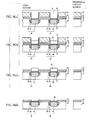
FIGS. 7(a) through 7(d) are cross-sectional views (1) of a flash memory and a manufacturing method thereof in accordance with a second embodiment; -
FIGs. 8(a) through 8(d) are respectively cross-sectional views (2) of the flash memory and the manufacturing method thereof in accordance with the second embodiment; -
FIGs. 9(a) through 9(d) are respectively cross-sectional views (3) of the flash memory and the manufacturing method thereof in accordance with the second embodiment; and -
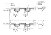
FIGs. 10(a) and 10(b) are respectively cross-sectional views (4) of the flash memory and the manufacturing method thereof in accordance with the second embodiment, - Hereinafter, the embodiments in accordance with the present invention will be explained with reference to the attached drawings.
- A flash memory and a manufacturing method thereof in accordance with a first embodiment are explained with reference to
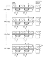
FIGs. 2(a)-2(d) toFIGs. 6(a)-6(e) .FIGs. 2(a) through 2(d) andFIGs. 3(a) through 3(d) are diagrams of a cross-sectional view in a bit line direction of a transistor forming a core. The left side is a core region of a memory cell and the right side is a peripheral circuit region.FIGs. 4(a) and 4(b) toFIGs. 6(a) through 6(e) are oblique top views and cross-sectional views. - In
FIG. 2(a) , a tunnel oxide film 12 (silicon oxide film), a trap layer 14 (silicon nitride film), and a top layer 16 (silicon oxide film) are formed on a P-type silicon semiconductor substrate 10 (or a P-type semiconductor region formed within the semiconductor substrate) as an oxide/nitride/oxide (ONO)film 18. Thetunnel oxide film 12 is formed by, for example, a thermal oxidization method, and thetrap layer 14 and thetop oxide film 16 are formed by, for example, a chemical vapor deposition (CVD) method. TheONO film 18 in the peripheral circuit region is removed and a gate oxide film 70 (silicon oxide film) is formed by, for example, the thermal oxidization method. - In
FIG. 2(b) , a firstpolycrystalline silicon film 30 that becomesgate electrodes FIG. 2(c) , the firstpolycrystalline silicon film 30 of a region forming abit line 28 is etched and an opening region is formed. Subsequently, a lowconcentration diffusion region 24 is formed by implanting arsenic in thesemiconductor substrate 10, for example, at an implantation energy of 30 keV and an implantation dosage of 5x1014 cm-2, using the firstpolycrystalline silicon film 30 that is the mask layer as a mask, and subsequently performing heat-treatment thereto. In other words, the lowconcentration diffusion region 24 composing thebit line 28, which is buried in thesemiconductor substrate 10 and includes a source region and a drain region, is formed through ion implantation using the mask layer formed on theONO film 18 as the mask. Furthermore, pocketimplantation diffusion regions 26 are formed on both sides of the lowconcentration diffusion region 24, by performing pocket-implantation using boron, for example, at an implantation energy of 30 keV, an implantation dosage of 4x1013 cm-2, and an ion irradiation angle of 15° to the vertical line of the semiconductor substrate and subsequently performing heat-treatment thereto. In other words, the pocketimplantation diffusion regions 26 are formed on both sides of the lowconcentration diffusion region 24 in the width direction by performing pocket-implantation using the mask layer as the mask. Short channel effect of the transistor can be prevented by the formation of the pocketimplantation diffusion regions 26. - In
FIG. 2(d) , asidewall film 32 having a film thickness of 50 nm is formed with, for example, silicon oxide film on the firstpolycrystalline silicon film 30. InFIG. 3(a) , sidewalls 33 are formed on the side surfaces of the firstpolycrystalline film 30 in the bit line 28-width direction by etching. The film thickness of thesidewall film 32 can control the width of thesidewall 32. If the film thickness of thesidewall film 32 is 10 nm, the width of thesidewall 32 can be about 7 nm. The sidewall 3 can be an insulating film or metal. A highconcentration diffusion region 22 is formed by implanting arsenic, for example, at an implantation energy of 40 keV and an implantation dosage of 2x1015 cm-2, in thesemiconductor substrate 10 using the firstpolycrystalline silicon film 30 and thesidewalls 33 as the mask, and subsequently performing heat-treatment thereto. In other words, the highconcentration diffusion region 24 that composes thebit line 28 and has a higher impurity concentration than the lowconcentration diffusion region 24 is formed by ion implantation using the mask layer and thesidewalls 33 formed on the side surfaces of the mask layer as the mask. - In
FIG. 3(b) , asilicon oxide film 36 is formed to bury the opening region and cover thepolycrystalline silicon film 30. InFIG. 3(c) , thesilicon oxide film 36 is left remaining in the opening region of the firstpolycrystalline silicon film 30 by planarization through a chemical mechanical planarization (CMP) method. -
FIGs. 4(a) and 4(b) are diagrams of a dimensional configuration at this stage.FIG. 4(a) is an oblique top view. The left side is a core region and the right side is a peripheral circuit region. In addition, thesidewalls 33, thesemiconductor substrate 10, and theONO film 18 are not shown.FIG. 4(b) is a cross-sectional view taken along line A-A. Thebit line 28 is formed within thesemiconductor substrate 10 in the core region. TheONO film 18 is formed in the core region and agate oxide film 70 is formed in the peripheral circuit region, on the entire surface of thesemiconductor substrate 10. Thesilicon oxide film 36 is formed on thebit line 28. The firstpolycrystalline silicon film 30 is formed on theONO film 18, in the regions other than thebit line 28, or thegate oxide film 70. - In
FIGs. 5(a) through 5(d) , a second polycrystalline silicon layer 34 (metal layer) is formed on the entire surface.FIG. 5(a) is an oblique top view. The left side is the core region and the right side is the peripheral circuit region.FIG. 5(b) is a cross-sectional view taken along line A-A, in the width direction of thebit line 28.FIG. 5(c) is a cross-sectional view taken along line B-B, in the length direction of thebit line 28 in thebit line 28 region.FIG 5(d) is a cross-sectional view taken along line C-C, in the length direction of thebit line 28 in the region between the bit lines 28. In thebit line 28 region, theONO film 18 is formed on thebit line 28, and thesilicon oxide film 36 and the second polycrystalline silicon film 34 (metal layer) are laminated onto theONO film 18. In the region between the bit lines 28, theONO film 18 is formed on thebit line 28, and the firstpolycrystalline silicon film 30 and the second polycrystalline silicon film 34 (metal layer) are laminated onto theONO film 18. - In
FIG. 3(d) andFIGs. 6(a) through 6(e) , thegate electrode 31 that includes the word line, including a metal layer intersecting with thebit line 28, and the mask layer is formed by etching the second polycrystalline silicon film 34 (metal layer) and the first polycrystalline silicon layer 30 (mask layer).FIG. 6(a) is an oblique top view. The left side is the core region and the right side is the peripheral circuit region.FIG. 6(b) is a cross-sectional view taken along line A-A, in the length direction of theword line 35 in theword line 35 region.FIG. 6(c) is a cross-sectional view taken along line B-B, in the length direction of theword line 35 in the region between the word lines 35.FIG. 6(d) is a cross-sectional view taken along line C-C, in the length direction of thebit line 28 in thebit line 28 region.FIG. 6(e) is a cross-sectional view taken along line D-D, in the length direction of thebit line 28 in the region between the bit lines 28. - In the core region, the
ONO layer 18 is formed on thebit line 28 under theword line 35 and thesilicon oxide film 36 is formed on theONO layer 18. TheONO layer 18 is formed in region between the bit lines 28 under theword line 35 and thegate electrode 31 is formed on theONO layer 18. TheONO layer 18 is formed on thebit line 28 in the region between the word lines 35 and only thesilicon oxide film 36 is formed on theONO layer 18. Only theONO layer 18 is formed in the region between the bit lines 28 in the region between the word lines 35. In the peripheral circuit region, thegate electrode 38 composed of the firstpolycrystalline silicon film 30 and the secondpolycrystalline film 34 is formed on thegate oxide film 70 in the gate formation region. In this way, thegate electrode 31 in the core region, theword line 35 connecting on thegate electrode 31, and thegate electrode 38 in the peripheral circuit region are formed simultaneously by the simultaneous etching of the two layers of polycrystalline silicon film. - Subsequently, in the peripheral circuit region, a transistor for the peripheral circuit is formed. An interlayer insulating film having contact holes is formed. An interconnection layer connecting to the
bit line 28 via the contact hole is formed. Lastly, a protective film is formed, and the flash memory in accordance with the first embodiment is completed, - In the first embodiment, the semiconductor device includes: the
gate electrode 31 provided on thesemiconductor substrate 10; theONO film 18 that is formed between thegate electrode 31 and thesemiconductor substrate 10 and has a charge storage region under the gate electrode; and abit line 28 that is buried in thesemiconductor substrate 10 and includes the lowconcentration diffusion region 24, the highconcentration diffusion region 22 that is formed in the center of the low concentration diffusion region and has a higher impurity concentration than the low concentration diffusion region, the source region, and the drain region. In thebit line 28, the lowconcentration diffusion region 24 having a low concentration is formed within the highconcentration diffusion region 22 from the perspective of thegate electrode 31. This is the so-called lightly-doped drain (LDD) structure. In this way, the decrease in the source-drain breakdown voltage of the transistor can be prevented even when the highconcentration diffusion region 22 is formed by high-energy, high-dosage ion-implantation to reduce the resistance of thebit line 28. - In addition, the dispersal of impurities in the low concentration diffusion region is small due also to the heat treatment procedure after the
bit line 28 formation, and thus, the fluctuation in the transistor characteristics can be prevented. Furthermore, thesemiconductor substrate 10 and the contact hole for connecting with the interconnection layer never connect, even when the contact hole moves from the highconcentration diffusion region 22, because the lowconcentration diffusion region 24 is provided. As a result, the flow of the junction current between thesemiconductor substrate 10 and the contact hole and the flow of a leak current between thebit line 28 and thesemiconductor substrate 10 can be prevented. - In this way, the first
polycrystalline silicon film 30 in which the mask layer when thebit line 28 is formed is metal allows the lowconcentration diffusion region 24 to be formed on both sides of the highconcentration diffusion region 22, due to the sidewalls provided on the side surfaces of the first polycrystalline silicon (gate electrode) 30. If the bit line is formed using aphotoresist 60 as in Conventional Art 1, sidewalls cannot be formed on the side surfaces thereof because the photoresist cannot be exposed to high temperatures. Therefore, the highconcentration diffusion region 22 and the lowconcentration diffusion region 24 are formed using separate photoresists as the masks and the overlapping dimension of the highconcentration diffusion region 22 and the lowconcentration diffusion region 24 cannot be made accurate. Thus, the fluctuation in the electrical characteristics of the transistor increases. - In the first embodiment, the high
concentration diffusion region 22 and the lowconcentration diffusion region 24 are formed by the formation of thesidewalls 33. The width of thesidewall 33 can be controlled by the thickness of thesidewall film 32, and thus, manufacturing can be performed with good control of the size, compared to using the amount of side-etching to control the size as in Conventional Art 2. Therefore, the fluctuation in the electrical characteristics of the transistor due to fluctuation in the sizes of the highconcentration diffusion region 22 and the lowconcentration diffusion region 24 can be prevented. - Furthermore, two charge storage regions are provided in the
ONO film 18 under thegate electrode 31 and theword line 35 that intersects with thebit line 28 and is connected to the gate electrode at an upper side thereof is provided, As a result, thebit line 28 can have the LDD structure even in a transistor having two or more charge storage regions in theONO film 18 under thegate electrode 31. - As in the first embodiment, the pocket
implantation diffusion regions 26 can be formed by pocket implantation when the lowconcentration diffusion region 24 is formed. In other words, thebit line 28 and the pocketimplantation diffusion regions 26 formed on both sides of the lowconcentration diffusion region 24 in the bit line width direction can be included. As a result, the short channel effect of the transistor can be suppressed. Furthermore, in the first embodiment, the mask layer forming thebit line 28 is thegate electrode 31, and thus, the manufacturing steps can be reduced. - The flash memory and the manufacturing method thereof in accordance with a second embodiment are explained with reference to
FIGs. 7(a) to 10(b) . These figures are cross-dimensional views of the transistor forming the core in the bit line width direction. The left side is the core region of the memory cell and the right side is the peripheral circuit region. - In
FIG. 7(a) , thetunnel oxide film 12 and thetrap layer 14 are formed on thesemiconductor substrate 10, as in the first embodiment. A silicon oxide film is formed on thetrap layer 14 as theprotective layer 15. Theprotective layer 15 is a layer that protects thetrap layer 14 during the manufacturing process. Theprotective layer 15 is formed to be 10 nm or more by a thermal oxidization method or the CVD method. The removal of theprotective layer 15 is facilitated by the use of the silicon oxide film as theprotective layer 15, and thus, selectivity with the silicon nitride film that is thetrap layer 14 can be secured during removal. - In
FIG. 7(b) , a silicon nitride film is formed on theprotective layer 15 as amask layer 40. Here, subsequent etching of themask layer 40 is facilitated by the use of, for example, the silicon nitride film as themask layer 40 layer, and thus, selectivity with theprotective layer 15 can be secured during etching. Furthermore, in the subsequent silicided metal layer formation, the surface of the semiconductor substrate can be silicided selectively without siliciding the surface. - In
FIG. 7(c) , an opening region to form thebit line 28 is formed in themask layer 40. The lowconcentration diffusion region 24 is formed by implanting arsenic in thesemiconductor substrate 10, for example, at an implantation energy of 30 keV and an implantation dosage of 5x1014 cm-2, using themask layer 40 as the mask, and subsequently performing heat-treatment thereto. Furthermore, the pocketimplantation diffusion regions 26 are formed on both sides of the lowconcentration diffusion region 24 by performing pocket-implantation at an implantation energy of 30 keV and an implantation dosage of 4x10-13 cm-2, and subsequently performing heat-treatment thereto. - In
FIG. 7(d) , asidewall film 42 having a film thickness of 50 nm is formed with, for example, a silicon nitride film on themask layer 40. Themask layer 40 andsidewalls 43 can be subsequently removed simultaneously by the use of the same silicon nitride film as themask layer 40 for thesidewall film 40. InFIG. 8(a) , the entire surface of thesidewall film 42 is anisotropically dry-etched and thesidewalls 43 are formed on the side surfaces of themask layer 40 in thebit line 28 width direction. The film thickness of thesidewall film 42 can control the width of thesidewalls 43. - In
FIG. 8(b) , theprotective layer 15 and thetrap layer 14 are etched using themask layer 40 and thesidewalls 43 as the mask. InFIG. 8(c) , the highconcentration diffusion region 22 is formed by implanting arsenic in thesemiconductor substrate 10, for example, at an implantation energy of 40 keV and an implantation dosage of 2x1015 cm-2, using themask layer 40 and thesidewalls 43 as the mask, and subsequently performing heat-treatment thereto. The ion implantation energy can be reduced compared to using theONO film 18 as a through-film as in the first embodiment, by the use of only thetunnel oxide film 12 as the ion implantation through-film as such. Thus, dispersion of the ion-implanted impurities in the horizontal direction can be reduced. As a result, a furtherminiaturized bit line 28 can be formed. - In
FIG. 8(d) , thetunnel oxide film 12 is etched using themask layer 40 and thesidewalls 43 as the mask. Asilicided metal layer 50 is formed on the surface of thebit line 28 using themask layer 40 and thesidewalls 43 as the mask. The formation of thesilicided metal layer 50 is made by, for example, forming cobalt or titanium on the entire surface using a sputter technique and performing heat-treatment. The resistance of thebit line 28 can be reduced by the formation of thesilicided metal layer 50, formed consecutively in the length direction of thebit line 28. - In
FIG. 9(a) , aresin layer 52 is formed to cover themask layer 40 by the application of resin. HSQ (hydrogen-silsesquioxane), for example, can be used as the resin. InFIG. 9(b) , a portion of theresin layer 52 is removed by, for example, an ashing technique, and theresin layer 52 is left remaining on the silicided metal layer between the sidewalls 43. In other words, theresin layer 52 is selectively formed on the silicided metal layer. Here, theresin layer 52 preferably covers the side surfaces of thetrap layer 14. Themask layer 40 and thesidewalls 43 are removed by, for example, hot phosphoric acid. At this time, the side surfaces of thetrap layer 14, which is a silicon nitride film, is protected by theresin layer 52. Thus, themask layer 40 and thesidewalls 43 can be removed easily without removing thetrap layer 14. - In
FIG. 9(d) , theresin layer 52 is removed and theprotective layer 15 is removed. InFIG. 10 (a) , a silicon oxide film is formed on the surface of thetrap layer 14 and thesilicided metal layer 50 as thetop oxide film 16 using, for example, the CVD method. At this time, the temperature of formation is preferably a temperature that prevents oxidization of thesilicided metal layer 50, for example, below 800°C. In this way, theONO film 18 having atunnel oxide film 12, atrap layer 14, and atop oxide film 16 is formed. A satisfactory insulation characteristic between thesilicided metal layer 50 and aword line 58 can be acquired because thetop oxide film 16 is good membranous material that has not been exposed to ion implantation. - Finally, in
FIG. 10(b) , theONO film 18 in the peripheral circuit region is removed and agate oxide film 60 is formed. Theword line 58 that serves as the gate electrode is formed in the core region by deposition of a polycrystalline silicon film and etching of a predetermined region. Then, the transistor for the peripheral circuit is formed in the peripheral circuit region. Furthermore, the interlayer insulating film having contact holes is formed. The interconnection layer connecting with thebit line 28 is formed via the contact hole. Lastly, the protective layer is formed, and the flash memory in accordance with the second embodiment is completed. - In the second embodiment, the
bit line 28 has an LDD structure as in the first embodiment. As a result, the reduction in the source-drain breakdown voltage of the transistor can be prevented. In addition, the flow of the leak current between thebit line 28 and thesemiconductor substrate 10 can be prevented, even when the contact hole moves from the high concentration diffusion region. Furthermore, themask layer 40 is a silicon nitride film that is an insulating film and thesidewalls 43 can be formed on the side surfaces of themask layer 40. Thus, the fluctuation in the electrical characteristics of the transistor can be reduced. - In addition, the short channel effect of the transistor can be suppressed by the pocket implantation. Furthermore, the silicon nitride film is used as the
mask layer 40 in the second embodiment, and thus, thesilicided metal layer 50 can be formed selectively on thebit line 28. As a result, the resistance of the bit line can be reduced and the memory cells can be miniaturized. - Although the preferred embodiments of the present invention have been explained above, the present invention is not limited to the specific embodiments, and various changes and modifications can be made without departing from the principles and spirit of the invention, the scope of which is defined in the claims.
Claims (12)
- A semiconductor device comprising:a gate electrode located above a semiconductor substrate;an ONO film formed between the semiconductor substrate and the gate electrode and having a charge storage region under the gate electrode; anda bit line including a low concentration diffusion region, a high concentration diffusion region provided at center of the law concentration diffusion region and having a higher impurity concentration than the low concentration diffusion region, a source region and a drain region, and formed in the semiconductor substrate.
- The semiconductor device as claimed in claim 1, wherein the bit line includes pocket implantation diffusion regions formed at both sides of the low concentration diffusion region.
- The semiconductor device as claimed in claim 1 or 2, wherein the ONO film has multiple charge storage regions under the gate electrode.
- The semiconductor device as claimed in any of claims 1 to 3, further comprising a word line provided across the bit line and connected to the gate electrode at an upper side thereof.
- The semiconductor device as claimed in claim 4, further comprising sidewalls provided at sides of the gate electrode.
- The semiconductor device as claimed in any of claims 1 to 5, further comprising a silicided metal layer provided on the bit line and running in a length direction of the bit line continuously.
- A method of fabricating a semiconductor device comprising:forming an ONO film on a semiconductor substrate;forming a mask layer on the ONO film;forming a low concentration diffusion region by using the mask layer as a mask for ion implantation, the concentration diffusion region being included by a bit line including a source region and a drain region;forming sidewalls at both sides of the mask layer; andforming a high concentration diffusion region by using the mask layer and the sidewalls as a mask for ion implantation, the high concentration diffusion region having a higher impurity concentration than the low concentration diffusion regions and included by the bit line.
- A method as claimed in claim 7, further comprising forming pocket implantation diffusion regions, at both sides of the low concentration diffusion region, by using the mask layer as a mask for ion implantation.
- The method as claimed in claim 7 or 8, wherein the mask layer includes a metal or insulator.
- The method as claimed in claim 7 or 8, further comprising:forming a metal layer on the mask layer; andforming a word line by etching the metal layer and the mask layer, the word line including the metal layer and a gate electrode including the mask layer.
- The method as claimed in of claim 7 or 8, further comprising forming a silicided metal layer, on the bit line, by using the mask layer and the sidewalls as a mask.
- The method as claimed in claim 11, further comprising:selectively forming a resin layer on the silicided metal layer; andremoving the mask layer,wherein the resin layer covers side faces of a trap layer in the ONO film in the step of removing the mask layer.
Applications Claiming Priority (1)
| Application Number | Priority Date | Filing Date | Title |
|---|---|---|---|
| PCT/JP2005/008056 WO2006117851A1 (en) | 2005-04-27 | 2005-04-27 | Semiconducteur device and method for manufacturing same |
Publications (2)
| Publication Number | Publication Date |
|---|---|
| EP1895582A1 true EP1895582A1 (en) | 2008-03-05 |
| EP1895582A4 EP1895582A4 (en) | 2009-09-23 |
Family
ID=37307658
Family Applications (1)
| Application Number | Title | Priority Date | Filing Date |
|---|---|---|---|
| EP05737365A Withdrawn EP1895582A4 (en) | 2005-04-27 | 2005-04-27 | SEMICONDUCTOR COMPONENT AND METHOD FOR THE PRODUCTION THEREOF |
Country Status (6)
| Country | Link |
|---|---|
| US (1) | US7626227B2 (en) |
| EP (1) | EP1895582A4 (en) |
| JP (1) | JP5047786B2 (en) |
| CN (1) | CN101167180A (en) |
| TW (1) | TW200644258A (en) |
| WO (1) | WO2006117851A1 (en) |
Families Citing this family (8)
| Publication number | Priority date | Publication date | Assignee | Title |
|---|---|---|---|---|
| US7678654B2 (en) * | 2006-06-30 | 2010-03-16 | Qimonda Ag | Buried bitline with reduced resistance |
| JP2009049138A (en) * | 2007-08-17 | 2009-03-05 | Spansion Llc | Manufacturing method of semiconductor device |
| JP5379366B2 (en) * | 2007-09-20 | 2013-12-25 | スパンション エルエルシー | Semiconductor device and manufacturing method thereof |
| JP5274878B2 (en) * | 2008-04-15 | 2013-08-28 | パナソニック株式会社 | Semiconductor device and manufacturing method thereof |
| US8653581B2 (en) * | 2008-12-22 | 2014-02-18 | Spansion Llc | HTO offset for long Leffective, better device performance |
| US7943983B2 (en) * | 2008-12-22 | 2011-05-17 | Spansion Llc | HTO offset spacers and dip off process to define junction |
| CN106876401B (en) * | 2017-03-07 | 2018-10-30 | 长江存储科技有限责任公司 | The forming method of memory device |
| JP2020145290A (en) * | 2019-03-05 | 2020-09-10 | キオクシア株式会社 | Semiconductor storage device |
Family Cites Families (20)
| Publication number | Priority date | Publication date | Assignee | Title |
|---|---|---|---|---|
| JP3397804B2 (en) * | 1992-06-09 | 2003-04-21 | シチズン時計株式会社 | Manufacturing method of nonvolatile memory |
| US6768165B1 (en) | 1997-08-01 | 2004-07-27 | Saifun Semiconductors Ltd. | Two bit non-volatile electrically erasable and programmable semiconductor memory cell utilizing asymmetrical charge trapping |
| US6348711B1 (en) * | 1998-05-20 | 2002-02-19 | Saifun Semiconductors Ltd. | NROM cell with self-aligned programming and erasure areas |
| JP2000260890A (en) * | 1999-03-12 | 2000-09-22 | Nec Corp | Nonvolatile memory and manufacture of the same |
| JP2001148434A (en) * | 1999-10-12 | 2001-05-29 | New Heiro:Kk | Nonvolatile memory cell, method of using the same, manufacturing method, and nonvolatile memory array |
| US6248633B1 (en) * | 1999-10-25 | 2001-06-19 | Halo Lsi Design & Device Technology, Inc. | Process for making and programming and operating a dual-bit multi-level ballistic MONOS memory |
| JP4923318B2 (en) * | 1999-12-17 | 2012-04-25 | ソニー株式会社 | Nonvolatile semiconductor memory device and operation method thereof |
| US6417081B1 (en) * | 2000-05-16 | 2002-07-09 | Advanced Micro Devices, Inc. | Process for reduction of capacitance of a bitline for a non-volatile memory cell |
| US7125763B1 (en) * | 2000-09-29 | 2006-10-24 | Spansion Llc | Silicided buried bitline process for a non-volatile memory cell |
| JP4051175B2 (en) * | 2000-11-17 | 2008-02-20 | スパンション エルエルシー | Nonvolatile semiconductor memory device and manufacturing method |
| JP4083975B2 (en) * | 2000-12-11 | 2008-04-30 | 株式会社ルネサステクノロジ | Semiconductor device |
| US6559010B1 (en) * | 2001-12-06 | 2003-05-06 | Macronix International Co., Ltd. | Method for forming embedded non-volatile memory |
| KR100549320B1 (en) * | 2002-02-21 | 2006-02-02 | 마츠시타 덴끼 산교 가부시키가이샤 | Semiconductor storage device and its manufacturing method |
| JP2004095893A (en) * | 2002-08-30 | 2004-03-25 | Nec Electronics Corp | Semiconductor storage device, its control method and its manufacturing method |
| JP2004253571A (en) | 2003-02-19 | 2004-09-09 | Seiko Epson Corp | Semiconductor device manufacturing method and semiconductor device |
| US6754105B1 (en) * | 2003-05-06 | 2004-06-22 | Advanced Micro Devices, Inc. | Trench side wall charge trapping dielectric flash memory device |
| JP4818578B2 (en) * | 2003-08-06 | 2011-11-16 | ルネサスエレクトロニクス株式会社 | Nonvolatile semiconductor memory device and manufacturing method thereof |
| US6987048B1 (en) * | 2003-08-06 | 2006-01-17 | Advanced Micro Devices, Inc. | Memory device having silicided bitlines and method of forming the same |
| US6939767B2 (en) * | 2003-11-19 | 2005-09-06 | Freescale Semiconductor, Inc. | Multi-bit non-volatile integrated circuit memory and method therefor |
| US7151293B1 (en) * | 2004-08-27 | 2006-12-19 | Spansion, Llc | SONOS memory with inversion bit-lines |
-
2005
- 2005-04-27 JP JP2007514420A patent/JP5047786B2/en not_active Expired - Lifetime
- 2005-04-27 EP EP05737365A patent/EP1895582A4/en not_active Withdrawn
- 2005-04-27 CN CNA2005800495925A patent/CN101167180A/en active Pending
- 2005-04-27 WO PCT/JP2005/008056 patent/WO2006117851A1/en not_active Ceased
-
2006
- 2006-04-27 TW TW095115025A patent/TW200644258A/en unknown
- 2006-04-27 US US11/414,082 patent/US7626227B2/en not_active Expired - Lifetime
Also Published As
| Publication number | Publication date |
|---|---|
| JPWO2006117851A1 (en) | 2008-12-18 |
| EP1895582A4 (en) | 2009-09-23 |
| JP5047786B2 (en) | 2012-10-10 |
| US7626227B2 (en) | 2009-12-01 |
| CN101167180A (en) | 2008-04-23 |
| WO2006117851A1 (en) | 2006-11-09 |
| TW200644258A (en) | 2006-12-16 |
| US20070045720A1 (en) | 2007-03-01 |
Similar Documents
| Publication | Publication Date | Title |
|---|---|---|
| CN113597676B (en) | Fabrication process of NOR memory cell with vertical floating gate | |
| US7767522B2 (en) | Semiconductor device and a method of manufacturing the same | |
| US9379127B2 (en) | Semiconductor device and manufacturing method of semiconductor device | |
| US20020130314A1 (en) | Non-volatile memory device having a metal-oxide-nitride-oxide-semiconductor gate structure and fabrication method thereof | |
| EP0997930A1 (en) | Integration method for sidewall split gate flash transistor | |
| US9905429B2 (en) | Semiconductor device and a manufacturing method thereof | |
| US7626227B2 (en) | Semiconductor device with reduced transistor breakdown voltage for preventing substrate junction currents | |
| US9379128B1 (en) | Split gate non-volatile memory device and method for fabricating the same | |
| US8207560B2 (en) | Nonvolatile semiconductor memory device and method of fabricating the same | |
| US6812099B2 (en) | Method for fabricating non-volatile memory having P-type floating gate | |
| US6436800B1 (en) | Method for fabricating a non-volatile memory with a shallow junction | |
| EP1898460B1 (en) | Semiconductor device and fabrication method thereof | |
| US7772639B2 (en) | Charge-trap nonvolatile memory devices | |
| CN100505219C (en) | Method for the manufacture of a non-volatile memory device and memory device thus obtained | |
| US8901637B2 (en) | Semiconductor memory device having lowered bit line resistance | |
| US7109084B2 (en) | Flash memory device and method for fabricating the same | |
| US8097518B2 (en) | Semiconductor device and manufacturing method therefor | |
| US9269583B1 (en) | Method for fabricating memory device | |
| KR20070090027A (en) | Semiconductor device and manufacturing method thereof | |
| KR20070119052A (en) | Semiconductor device and manufacturing method thereof |
Legal Events
| Date | Code | Title | Description |
|---|---|---|---|
| PUAI | Public reference made under article 153(3) epc to a published international application that has entered the european phase |
Free format text: ORIGINAL CODE: 0009012 |
|
| 17P | Request for examination filed |
Effective date: 20070928 |
|
| AK | Designated contracting states |
Kind code of ref document: A1 Designated state(s): DE FR GB |
|
| DAX | Request for extension of the european patent (deleted) | ||
| RBV | Designated contracting states (corrected) |
Designated state(s): DE FR GB |
|
| A4 | Supplementary search report drawn up and despatched |
Effective date: 20090825 |
|
| 17Q | First examination report despatched |
Effective date: 20130612 |
|
| RAP1 | Party data changed (applicant data changed or rights of an application transferred) |
Owner name: SPANSION JAPAN LIMITED Owner name: CYPRESS SEMICONDUCTOR CORPORATION |
|
| STAA | Information on the status of an ep patent application or granted ep patent |
Free format text: STATUS: EXAMINATION IS IN PROGRESS |
|
| STAA | Information on the status of an ep patent application or granted ep patent |
Free format text: STATUS: THE APPLICATION IS DEEMED TO BE WITHDRAWN |
|
| 18D | Application deemed to be withdrawn |
Effective date: 20171103 |