EP1895498A2 - Pixel circuit, display including the same, and driving method thereof - Google Patents
Pixel circuit, display including the same, and driving method thereof Download PDFInfo
- Publication number
- EP1895498A2 EP1895498A2 EP07253427A EP07253427A EP1895498A2 EP 1895498 A2 EP1895498 A2 EP 1895498A2 EP 07253427 A EP07253427 A EP 07253427A EP 07253427 A EP07253427 A EP 07253427A EP 1895498 A2 EP1895498 A2 EP 1895498A2
- Authority
- EP
- European Patent Office
- Prior art keywords
- transistor
- coupled
- electrode
- power supply
- pixel circuit
- Prior art date
- Legal status (The legal status is an assumption and is not a legal conclusion. Google has not performed a legal analysis and makes no representation as to the accuracy of the status listed.)
- Withdrawn
Links
Images



Classifications
-
- G—PHYSICS
- G09—EDUCATION; CRYPTOGRAPHY; DISPLAY; ADVERTISING; SEALS
- G09G—ARRANGEMENTS OR CIRCUITS FOR CONTROL OF INDICATING DEVICES USING STATIC MEANS TO PRESENT VARIABLE INFORMATION
- G09G3/00—Control arrangements or circuits, of interest only in connection with visual indicators other than cathode-ray tubes
- G09G3/20—Control arrangements or circuits, of interest only in connection with visual indicators other than cathode-ray tubes for presentation of an assembly of a number of characters, e.g. a page, by composing the assembly by combination of individual elements arranged in a matrix no fixed position being assigned to or needed to be assigned to the individual characters or partial characters
- G09G3/22—Control arrangements or circuits, of interest only in connection with visual indicators other than cathode-ray tubes for presentation of an assembly of a number of characters, e.g. a page, by composing the assembly by combination of individual elements arranged in a matrix no fixed position being assigned to or needed to be assigned to the individual characters or partial characters using controlled light sources
- G09G3/30—Control arrangements or circuits, of interest only in connection with visual indicators other than cathode-ray tubes for presentation of an assembly of a number of characters, e.g. a page, by composing the assembly by combination of individual elements arranged in a matrix no fixed position being assigned to or needed to be assigned to the individual characters or partial characters using controlled light sources using electroluminescent panels
- G09G3/32—Control arrangements or circuits, of interest only in connection with visual indicators other than cathode-ray tubes for presentation of an assembly of a number of characters, e.g. a page, by composing the assembly by combination of individual elements arranged in a matrix no fixed position being assigned to or needed to be assigned to the individual characters or partial characters using controlled light sources using electroluminescent panels semiconductive, e.g. using light-emitting diodes [LED]
- G09G3/3208—Control arrangements or circuits, of interest only in connection with visual indicators other than cathode-ray tubes for presentation of an assembly of a number of characters, e.g. a page, by composing the assembly by combination of individual elements arranged in a matrix no fixed position being assigned to or needed to be assigned to the individual characters or partial characters using controlled light sources using electroluminescent panels semiconductive, e.g. using light-emitting diodes [LED] organic, e.g. using organic light-emitting diodes [OLED]
- G09G3/3225—Control arrangements or circuits, of interest only in connection with visual indicators other than cathode-ray tubes for presentation of an assembly of a number of characters, e.g. a page, by composing the assembly by combination of individual elements arranged in a matrix no fixed position being assigned to or needed to be assigned to the individual characters or partial characters using controlled light sources using electroluminescent panels semiconductive, e.g. using light-emitting diodes [LED] organic, e.g. using organic light-emitting diodes [OLED] using an active matrix
- G09G3/3233—Control arrangements or circuits, of interest only in connection with visual indicators other than cathode-ray tubes for presentation of an assembly of a number of characters, e.g. a page, by composing the assembly by combination of individual elements arranged in a matrix no fixed position being assigned to or needed to be assigned to the individual characters or partial characters using controlled light sources using electroluminescent panels semiconductive, e.g. using light-emitting diodes [LED] organic, e.g. using organic light-emitting diodes [OLED] using an active matrix with pixel circuitry controlling the current through the light-emitting element
-
- G—PHYSICS
- G09—EDUCATION; CRYPTOGRAPHY; DISPLAY; ADVERTISING; SEALS
- G09G—ARRANGEMENTS OR CIRCUITS FOR CONTROL OF INDICATING DEVICES USING STATIC MEANS TO PRESENT VARIABLE INFORMATION
- G09G2300/00—Aspects of the constitution of display devices
- G09G2300/08—Active matrix structure, i.e. with use of active elements, inclusive of non-linear two terminal elements, in the pixels together with light emitting or modulating elements
- G09G2300/0809—Several active elements per pixel in active matrix panels
- G09G2300/0819—Several active elements per pixel in active matrix panels used for counteracting undesired variations, e.g. feedback or autozeroing
-
- G—PHYSICS
- G09—EDUCATION; CRYPTOGRAPHY; DISPLAY; ADVERTISING; SEALS
- G09G—ARRANGEMENTS OR CIRCUITS FOR CONTROL OF INDICATING DEVICES USING STATIC MEANS TO PRESENT VARIABLE INFORMATION
- G09G2300/00—Aspects of the constitution of display devices
- G09G2300/08—Active matrix structure, i.e. with use of active elements, inclusive of non-linear two terminal elements, in the pixels together with light emitting or modulating elements
- G09G2300/0809—Several active elements per pixel in active matrix panels
- G09G2300/0842—Several active elements per pixel in active matrix panels forming a memory circuit, e.g. a dynamic memory with one capacitor
- G09G2300/0852—Several active elements per pixel in active matrix panels forming a memory circuit, e.g. a dynamic memory with one capacitor being a dynamic memory with more than one capacitor
-
- G—PHYSICS
- G09—EDUCATION; CRYPTOGRAPHY; DISPLAY; ADVERTISING; SEALS
- G09G—ARRANGEMENTS OR CIRCUITS FOR CONTROL OF INDICATING DEVICES USING STATIC MEANS TO PRESENT VARIABLE INFORMATION
- G09G2300/00—Aspects of the constitution of display devices
- G09G2300/08—Active matrix structure, i.e. with use of active elements, inclusive of non-linear two terminal elements, in the pixels together with light emitting or modulating elements
- G09G2300/0809—Several active elements per pixel in active matrix panels
- G09G2300/0842—Several active elements per pixel in active matrix panels forming a memory circuit, e.g. a dynamic memory with one capacitor
- G09G2300/0861—Several active elements per pixel in active matrix panels forming a memory circuit, e.g. a dynamic memory with one capacitor with additional control of the display period without amending the charge stored in a pixel memory, e.g. by means of additional select electrodes
-
- G—PHYSICS
- G09—EDUCATION; CRYPTOGRAPHY; DISPLAY; ADVERTISING; SEALS
- G09G—ARRANGEMENTS OR CIRCUITS FOR CONTROL OF INDICATING DEVICES USING STATIC MEANS TO PRESENT VARIABLE INFORMATION
- G09G2310/00—Command of the display device
- G09G2310/02—Addressing, scanning or driving the display screen or processing steps related thereto
- G09G2310/0262—The addressing of the pixel, in a display other than an active matrix LCD, involving the control of two or more scan electrodes or two or more data electrodes, e.g. pixel voltage dependent on signals of two data electrodes
-
- G—PHYSICS
- G09—EDUCATION; CRYPTOGRAPHY; DISPLAY; ADVERTISING; SEALS
- G09G—ARRANGEMENTS OR CIRCUITS FOR CONTROL OF INDICATING DEVICES USING STATIC MEANS TO PRESENT VARIABLE INFORMATION
- G09G2320/00—Control of display operating conditions
- G09G2320/04—Maintaining the quality of display appearance
- G09G2320/043—Preventing or counteracting the effects of ageing
-
- G—PHYSICS
- G09—EDUCATION; CRYPTOGRAPHY; DISPLAY; ADVERTISING; SEALS
- G09G—ARRANGEMENTS OR CIRCUITS FOR CONTROL OF INDICATING DEVICES USING STATIC MEANS TO PRESENT VARIABLE INFORMATION
- G09G2320/00—Control of display operating conditions
- G09G2320/04—Maintaining the quality of display appearance
- G09G2320/043—Preventing or counteracting the effects of ageing
- G09G2320/045—Compensation of drifts in the characteristics of light emitting or modulating elements
-
- G—PHYSICS
- G09—EDUCATION; CRYPTOGRAPHY; DISPLAY; ADVERTISING; SEALS
- G09G—ARRANGEMENTS OR CIRCUITS FOR CONTROL OF INDICATING DEVICES USING STATIC MEANS TO PRESENT VARIABLE INFORMATION
- G09G3/00—Control arrangements or circuits, of interest only in connection with visual indicators other than cathode-ray tubes
- G09G3/20—Control arrangements or circuits, of interest only in connection with visual indicators other than cathode-ray tubes for presentation of an assembly of a number of characters, e.g. a page, by composing the assembly by combination of individual elements arranged in a matrix no fixed position being assigned to or needed to be assigned to the individual characters or partial characters
- G09G3/2007—Display of intermediate tones
- G09G3/2014—Display of intermediate tones by modulation of the duration of a single pulse during which the logic level remains constant
Definitions
- FIG. 2 is a circuit diagram of a pixel circuit according to an embodiment of the present invention.
- a voltage variation amount may be large, i.e., ⁇ V N2 is large.
- a voltage variation amount of the first node N1 is determined corresponding to a voltage variation amount of the second node N2, which is a large value, i.e., ⁇ V N1 is large.
Landscapes
- Engineering & Computer Science (AREA)
- Physics & Mathematics (AREA)
- Computer Hardware Design (AREA)
- General Physics & Mathematics (AREA)
- Theoretical Computer Science (AREA)
- Control Of Indicators Other Than Cathode Ray Tubes (AREA)
- Control Of El Displays (AREA)
- Electroluminescent Light Sources (AREA)
- Liquid Crystal Display Device Control (AREA)
Abstract
Description
- The present invention relates to a pixel circuit, a display including the same, and a driving method thereof. More particularly, the present invention relates to a pixel circuit including a feedback feature, a display including the same, and a driving method thereof.
- Recently, various flat panel displays with reduced weight and volume compared to cathode ray tubes (CRTs) have been developed. Such flat panel displays include, liquid crystal displays (LCDs), field emission displays (FEDs), plasma display panels (PDPs), and organic light emitting displays.
- Among such flat panel displays, the organic light emitting displays may make use of organic light emitting diodes (OLEDs), which may emit light by recombination of electrons and holes. The organic light emitting display may offer various advantages, e.g., high response speed and low power consumption.
- A pixel of a conventional organic light emitting display includes an OLED and a pixel circuit. The pixel circuit may be coupled to a data line and a scan line, and may control the OLED. An anode electrode of the OLED may be coupled to the pixel circuit, and a cathode electrode thereof may be coupled to a power supply, e.g., ELVSS. The OLED may generate light of a predetermined luminance corresponding to an electric current provided by the pixel circuit. In particular, when a scan signal is supplied to the scan line, the pixel circuit may control the amount of an electric current provided to the OLED in correspondence with a data signal provided to the data line.
- The pixel circuit may include first and second transistors and a storage capacitor. The first transistor may control an amount of an electric current flowing from a power supply ELVDD to the power supply ELVSS through an OLED according to a voltage charged in the storage capacitor, and the OLED may emit light corresponding to the amount of an electric current supplied from the first transistor. The second transistor may be coupled between the data line and the scan line. The second transistor coupled to the scan line and the data line may controllably provide a data signal from the data line to the storage capacitor, and the storage capacitor may be charged with a voltage corresponding to the data signal.
- The above-described pixel circuit of the conventional organic light emitting display may not be entirely satisfactory, as a display including a plurality of such pixel circuits may not display an image of uniform luminance. In detail, threshold voltages of the drive transistors in the pixel circuits may be different depending on, e.g., fabrication process variations. When the threshold voltages of the drive transistors are different, the OLEDs in the display may emit light of differing luminances even though a data signal representing a same gradation is supplied to each of the pixel circuits.
- One approach to overcoming such drawbacks is to provide a pixel circuit that includes threshold voltage compensation for the drive transistor. However, such threshold voltage compensation may require six or more transistors in each pixel circuit, as well as additional wiring for controlling the transistors. Moreover, when six or more transistors are included in the pixel circuit, the structure of the pixel circuit may become complex. Furthermore, the above-described threshold voltage compensation may not compensate for other factors such as the carrier mobility of the drive transistor.
- The present invention is therefore directed to a pixel circuit, a display including the same, and a driving method thereof, which substantially overcome one or more of the problems due to the limitations and disadvantages of the
- It is therefore a feature of an embodiment of the present invention to provide a pixel circuit configured to provide feedback to a drive transistor.
- It is therefore another feature of an embodiment of the present invention to provide a pixel circuit configured to partially or fully compensate for variations in characteristics of a drive transistor.
- According to a first aspect of the invention there is provided a pixel circuit as set out in Claim 1. Preferred features of this aspect are set out in Claims 2 to 8. According to a second aspect of the invention there is provided a display as set out in Claim 9. Preferred features of this aspect are set out in Claims 10 and 11. According to a third aspect of the invention there is provided a method as set out in Claim 12. Preferred features of this aspect are set out in Claims 13 to 15.
- The above and other features and advantages of the present invention will become more apparent to those of ordinary skill in the art from the following detailed description of exemplary embodiments thereof with reference to the attached drawings, in which:
- FIG. 1 illustrates a display according to an embodiment of the present invention;
- FIG. 2 is a circuit diagram of a pixel circuit according to an embodiment of the present invention;
- FIG. 3 is a waveform diagram in a method of driving the pixel circuit shown in FIG. 2;
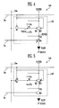
- FIGS. 4 and 5 are circuit diagrams of operational states in a method of driving the pixel circuit shown in FIG. 2; and
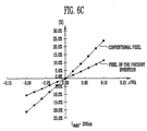
- FIGS. 6A-6C are graphs showing variations of electric current flowing through a pixel circuit according to a variation of a threshold voltage for a pixel circuit according to an embodiment of the present invention and a conventional pixel circuit.
- The present invention will now be described more fully hereinafter with reference to the accompanying drawings, in which exemplary embodiments of the invention are illustrated. The invention may, however, be embodied in different forms and should not be construed as limited to the embodiments set forth herein. Rather, these embodiments are provided so that this disclosure will be thorough and complete, and will fully convey the scope of the invention to those skilled in the art.
- Where an element is shown connected or coupled to a second element, the element may be directly connected or coupled to second element, or may be indirectly connected or coupled to second element via one or more other elements. In the drawings, elements may be omitted for clarity. Like reference numerals refer to like elements throughout.
- FIG. 1 illustrates a display according to an embodiment of the present invention. Referring to FIG. 1, the display according to a first embodiment of the present invention includes a
pixel portion 130, ascan driver 110, adata driver 120, and atiming control unit 150. Thepixel portion 130 includes a plurality ofpixels 140, which are coupled to scan lines S1 to Sn, emission control lines E1 to En, and data lines D1 to Dm. Thescan driver 110 drives the scan lines S1 to Sn and the emission control lines E1 to En. Thedata driver 120 drives the data lines D1 to Dm. Thetiming control unit 150 controls thescan driver 110 and thedata driver 120. - The
scan driver 110 receives a scan driving control signal SCS from thetiming control unit 150. Thescan driver 110 sequentially provides scan signals to the scan lines S1 through Sn. Further, thescan driver 110 sequentially provides emission control signals to the emission control lines E1 through En. - The
data driver 120 receives a data driving signal DCS from thetiming control unit 150. Further, thedata driver 120 provides data signals to the data lines D1 through Dm in synchronization with the scan signals. - The
timing control unit 150 provides the data driving signal DCS and the scan driving signal SCS corresponding to synchronizing signals supplied from an external source (not shown). Further, thetiming control unit 150 provides externally supplied data DATA to thedata driver 120. - The
pixel portion 130 receives external power from first and second power supplies ELVDD and ELVSS, respectively, and provides the power to thepixels 140. A voltage of the first power supply ELVDD is higher than that of the second power supply ELVSS. Thepixels 140 receives the power of the first power supply ELVDD and the power of the second power supply ELVSS, and generates light corresponding to a data signal. Emission times of thepixels 140 are controlled by an emission control signal. - FIG. 2 is a circuit diagram of a pixel circuit according to an embodiment of the present invention. In FIG. 2, a
pixel 140 is connected to an nth scan line Sn and an mth data line Dm. Referring to FIG. 2, thepixel 140 of the present invention includes an OLED and apixel circuit 142. Thepixel circuit 142 is connected to the data line Dm, the scan line Sn, and an nth emission control line En, and controls the OLED. - An anode electrode of the OLED is connected to the
pixel circuit 142, and a cathode electrode of the OLED may be connected to the second power supply ELVSS. The OLED generates light having a predetermined luminance corresponding to an electric current from thepixel circuit 142. - When the scan signal at a first level is supplied to the scan line Sn, the
pixel circuit 142 controls an amount of an electric current supplied to the OLED corresponding to a data signal, which is supplied to the data line Dm. A predetermined electric current from a drive transistor included in thepixel circuit 142 is supplied to the OLED, and a predetermined voltage is applied to the OLED. - As shown in FIG. 2, in the
pixel circuit 142 according to an embodiment of the present invention, thepixel circuit 142 provides a negative feedback of the predetermined voltage applied to the OLED to a gate electrode of a drive transistor. Thus, thepixel circuit 142 compensates for a threshold voltage and mobility of the drive transistor. - In detail, the
pixel circuit 142 includes first to fourth transistors M1 to M4, a storage capacitor Cst, and a feedback capacitor Cfb. A gate electrode of the first transistor M1 is coupled to the scan line Sn, and a first electrode thereof may be coupled to the data line Dm. Further, a second electrode of the first transistor M1 is coupled to a gate electrode of the second transistor M2, which is the drive transistor. - A gate electrode of the second transistor M2 is coupled to a second electrode of the first transistor M1, and a first electrode of the second transistor M2 is coupled to the first power supply ELVDD. Further, a second electrode of the second transistor M2 is coupled to a first electrode of the fourth transistor M4.
- A gate electrode of the third transistor M3 is coupled to the scan line Sn, and a first electrode of the third transistor M3 is coupled to the first power supply ELVDD. Further, a second electrode of the third transistor M3 is coupled to a first electrode of the fourth transistor M4.
- The first electrode of the fourth transistor M4 is coupled to the second electrode of the second transistor M2, and a second electrode of the fourth transistor M4 is coupled to the OLED. Further, a gate electrode of the fourth transistor M4 is coupled to the emission control line En. In other embodiments the fourth transistor M4 may be omitted, in which case the second electrode of the second transistor M2 is directly coupled to the anode electrode of the OLED.
- One electrode of the storage capacitor Cst is coupled to the gate electrode of the second transistor M2, and another electrode of the storage capacitor Cst is coupled to the first electrode of the second transistor M2. One electrode of the feedback capacitor Cfb is coupled to the gate electrode of the second transistor M2, and another electrode of the feedback capacitor Cfb is coupled to the second electrode of the second transistor M2.
- In operation of the
pixel circuit 142, when the scan signal at a first level is supplied to the scan line Sn, the first transistor M1 is turned on and transfers the data signal supplied to the data line Dm to the gate electrode of the second transistor M2. Also, when the first transistor M1 is turned-on, the storage capacitor Cst is charged with a voltage corresponding to the data signal. The second transistor M2 controls the amount of electric current from the first power supply ELVDD to the second power supply ELVSS through the OLED corresponding to the voltage applied to the gate electrode of the second transistor M2. The scan signal at the first level is also be supplied to the gate electrode of the third transistor M3, which transfers a voltage of the first power supply ELVDD to the first electrode of the fourth transistor M4. When the emission control signal at a second level is provided to the emission control line En, the fourth transistor M4 is turned-off, whereas, when the emission control signal at a first level is provided, the fourth transistor M4 is turned-on. The feedback capacitor Cfb is feeds back a voltage variation amount in the second electrode of the second transistor M2 to the gate electrode of the second transistor M2. - FIG. 3 is a waveform diagram in a method of driving the pixel circuit shown in FIG. 2. Referring to FIG. 3, an emission control signal applied to the emission control line En has a pulse width that is greater than the pulse width of a scan signal applied to the scan line Sn. For an emission control signal supplied to an ith emission control line Ei and a scan signal supplied to a corresponding ith scan line Si, the emission control signal can be at the first level when the scan signal is not at the first level. In other words, in this embodiment the emission control signal at the first level and the scan signal at the first level do not completely overlap.
- Referring to FIGS. 2 and 3, before the scan signal at the first level is supplied to the scan line Sn, the emission control signal at the first level is supplied to an emission control line En, which turns on the fourth transistor M4. Next, the scan signal at the first level is supplied to the scan line Sn, which turns on the first transistor M1 and the third transistor M3.
- FIGS. 4 and 5 are circuit diagrams of operational states in a method of driving the pixel circuit shown in FIG. 2. Referring to FIGS. 2-4, when the scan signal at the first level is provided to the scan line Sn and the first transistor M1 is turned-on, as shown in FIG. 4, a data voltage Vdata corresponding to a data signal is applied to a first node N1. Accordingly, the storage capacitor Cst is charged with a voltage corresponding to a difference between the data voltage Vdata and a first power supply ELVDD. Further, when the third transistor M3 is turned-on, a voltage of the first power supply ELVDD may be supplied to a second node N2.
- Thereafter, the scan signal is at the second level and the emission control signal may be at the first level. Accordingly, as shown in FIG. 5, the first transistor M1 and the third transistor M3 are turned-off, and the fourth transistor M4 is turned-on.
- At this time, the second transistor M2 transfers an electric current, corresponding to the voltage applied to the first node N1, to the OLED. In this case, a voltage of the second node N2 may change as expressed by equation 1 below.
-

- In Equation 1, VOLED represents a voltage applied to the OLED corresponding to an electric current flowing through the OLED. The voltage VOLED is increased in proportion to an amount of an electric current flowing through the OLED.
- With reference to the Equation 1, a voltage of the second node N2 decreases from the voltage of the first power supply ELVDD by a voltage applied to the OLED. Accordingly, a voltage of the first node N1 set in a floating state by the feedback capacitor Cfb can be varied. In practice, a voltage variation amount of the first node N1 may be as expressed by Equation 2 below.
-

- Thus, the voltage of the first node N1 may vary corresponding to a voltage variation amount of the second node N2. Because the voltage variation amount of the second node N2 may be associated with a threshold voltage of the second transistor M2, a voltage variation amount of the first node N1 changes corresponding to a threshold voltage of the second transistor M2.
- Next, the second transistor M2 transfers an electric current corresponding to a voltage applied to the first node N1 to the OLED, and the OLED generates light of a predetermined luminance corresponding to the electric current supplied thereto.
- As described above, the
pixel circuit 142 according to an embodiment of the present invention transfers the voltage applied to the OLED to a gate electrode of the second transistor M2, in correspondence with an amount of electric current supplied to the OLED from the second transistor M2, using a feedback capacitor Cfb. The electric current supplied to the OLED from the second transistor M2 may be affected by the threshold voltage of the second transistor M2. Thus, a non-uniformity in the threshold voltage of the second transistor M2 may be partially or fully compensated. This aspect of thepixel circuit 142 will be explained in additional detail with reference to Table 1 below.Table 1 Vth of M2 is small Vth of M2 is large IOLED large small VOLED large small ΔVN1 small large ΔVN2 small large ΔIOLED small large Final emission current IOLED(large)+ΔIOLED(small) IOLED(small)+ΔIOLED(large) - Table 1 presents a comparison of a smaller threshold voltage of the second transistor M2 and a larger threshold voltage thereof, for a same applied data signal. Referring to Table 1, when the threshold voltage Vth of the second transistor M2 is relatively small, a relatively large current is supplied to the OLED corresponding to a data signal, i.e., IOLED is large. In this case, a large voltage is applied to the OLED corresponding to an electric current supplied thereto, i.e., VOLED is large.
- In operation of the
pixel circuit 142, because the second node N2 changes to the voltage VOLED applied to the OLED from the first power supply ELVDD, a voltage variation amount is small, i.e., ΔVN2 is small. In the same manner, a voltage variation amount of the first node N1 is determined corresponding to a voltage variation amount of the second node N2, and is a small value, i.e., ΔVN1 is small. - When the voltage variation amount of the first node N1 is small, the amount of an electric current flowing through the OLED varies within a small range, i.e., ΔIOLED is small. As a result, the electric current flowing through the OLED only varies by a small current amount from the electric current IOLED corresponding to the data signal.
- By comparison, when the threshold voltage Vth of the second transistor M2 is relatively large, a small current is supplied to the OLED corresponding to the data signal, i.e., ΔIOLED is small. In this case, a lower voltage is supplied to the OLED, corresponding to the electric current supplied thereto, i.e., VOLED is small.
- In operation of the
pixel circuit 142, because the second node N2 changes to the voltage VOLED applied to the OLED from the first power supply ELVDD, a voltage variation amount may be large, i.e., ΔVN2 is large. In the same manner, a voltage variation amount of the first node N1 is determined corresponding to a voltage variation amount of the second node N2, which is a large value, i.e., ΔVN1 is large. - When the voltage variation amount of the first node N1 is large, the amount of electric current flowing through the OLED varies within a large range, i.e., ΔIOLED is large. As a result, the electric current flowing through the OLED varies by a large current amount from the electric current IOLED corresponding to the data signal.
- Thus, the
pixel circuit 142 according to an embodiment of the present invention changes an amount of electric current flowing into the OLED in correspondence with the threshold voltage of the second transistor M2. Accordingly, a display according to an embodiment of the present invention displays an image of uniform luminance. Moreover, thepixel circuit 142 according to an embodiment of the present invention may be used for apixel 140 having a relatively simple circuit of four transistors and two capacitors. - Another approach to providing a feedback voltage corresponding to an amount of an electric current flowing to the OLED is involves forming a pixel that includes a resistor having predetermined characteristics (not shown). However, it is difficult or impossible to form such a resistor having the same characteristics in every pixel using known manufacturing techniques. For example, a significant resistance deviation may occur among the pixel resistors, which may render such an approach unsuitable. In contrast, the
pixel circuit 142 according to an embodiment of the present invention feeds back the voltage applied to the OLED to the gate electrode of the second transistor M2 using a feedback capacitor Cfb. - FIGS. 6A-6C illustrate graphs showing variations of electric current flowing through a pixel circuit according to a variation of a threshold voltage for a pixel circuit according to an embodiment of the present invention and a conventional pixel circuit. Referring to FIG. 6A, when an electric current IOLED of 10 nA is supplied to the OLED, a large current (about 80 % of 10 nA) varies in a conventional pixel shown in FIG. 1, corresponding to a variation in the threshold voltage of the drive transistor. In contrast, in the
pixel circuit 142 according to an embodiment of the present invention, a small current (about 30 % of 10 nA) varies corresponding to a variation in the threshold voltage of the drive transistor. - Referring to FIG. 6B, when an electric current IOLED of 100 nA is supplied to the OLED, an electric current having a variation of about 35 % of 100 nA varies in a conventional pixel corresponding to a variation in the threshold voltage of the drive transistor. In contrast, an electric current having a variation of about 15 % of 100 nA varies corresponding to a variation in the threshold voltage of the drive transistor in the
pixel circuit 142 according to an embodiment of the present invention. - Referring to FIG. 6C, when an electric current IOLED of 200 nA is supplied to the OLED, an electric current having a variation of about 25 % of 200 nA varies in a conventional pixel corresponding to a variation in the threshold voltage of the drive transistor. In contrast, an electric current having a variation of about 12 % of 200 nA varies in the
pixel circuit 142 according to an embodiment of the present invention, corresponding to a variation in the threshold voltage of the drive transistor. Thus, in thepixel circuit 142 according to an embodiment of the present invention, a non-uniformity of the threshold voltage in the drive transistor may be partially or fully compensated. - As described above, since a pixel circuit, a display including the same, and a method for driving the display according to an embodiment of the present invention may provide a negative feedback of a voltage variation amount in a second electrode of a drive transistor to a gate electrode thereof, they may partially or fully compensate for non-uniformity of the threshold voltage in the drive transistor. Further, because the voltage feedback to the gate electrode of the drive transistor is determined according to an amount of an electric current flowing through the drive transistor, the mobility of the drive transistor may be partially or fully compensated. In addition, the pixel circuit according to an embodiment of the present invention compensates for variations in the threshold voltage of the drive transistor using only four transistors and two capacitors. Moreover, because each pixel may be coupled to one scan line, the need for additional wiring may be reduced.
- Exemplary embodiments of the present invention have been disclosed herein, and although specific terms are employed, they are used and are to be interpreted in a generic and descriptive sense only and not for purpose of limitation. For example, particular embodiments of the present invention have been described as being implemented using PMOS transistors. However, it will be understood that embodiments of the present invention may also be implemented using NMOS transistors and driving signals having levels corresponding to the NMOS transistors. Accordingly, it will be understood by those of ordinary skill in the art that various changes in form and details may be made without departing from the scope of the present invention as set forth in the following claims.
Claims (15)
- A pixel circuit, comprising:first, second, and third transistors, and first and second capacitors, wherein:the first transistor is controlled by a scan line and is configured to controllably couple a data line to the first capacitor and a gate electrode of the second transistor,the second transistor is further controlled by a voltage provided by the first and second capacitors,the third transistor is controlled by the scan line and is configured to controllably couple a first power supply to the second capacitor, andthe first power supply is controllably coupled to a light source by the second transistor.
- A pixel circuit according to claim 1, wherein the light source is an organic light emitting diode.
- A pixel circuit according to claim 1 or 2, wherein the first, second and third transistors are PMOS transistors.
- A pixel circuit according to any one of claims 1 to 3, wherein:the first transistor is configured to be turned-on when a scan signal at a first level is supplied to the scan line,the second transistor is configured to control an electric current flowing from the first power supply to a second power supply through the light source,the third transistor is configured to transfer a voltage of the first power supply to the second capacitor when the scan signal at the first level is supplied to the scan line,the first capacitor is coupled between the first transistor and the first power supply and is configured to be charged with a voltage corresponding to a data signal when the first transistor is turned on, andthe second capacitor is configured to regulate a voltage applied to a gate electrode of the second transistor based on a voltage output by the second transistor when an electric current is supplied to the light source.
- A pixel circuit according to any one of claims 1 to 4, wherein the first and second capacitors are both coupled to the gate electrode of the second transistor.
- A pixel circuit according to claim 5, wherein:a gate electrode of the first transistor is coupled to the scan line, and a first electrode of the first transistor is coupled to the data line,the gate electrode of the second transistor is coupled to a second electrode of the first transistor, and a first electrode of the second transistor is coupled to the first power supply,a gate electrode of the third transistor is coupled to the scan line, a first electrode of the third transistor is coupled to the first power supply, and a second electrode of the third transistor is coupled to a second electrode of the second transistor,a first electrode of the light source is coupled to the second electrode of the second transistor, and a second electrode of the light source is coupled to a second power supply,the first capacitor is coupled between the gate electrode and the first electrode of the second transistor, andthe second capacitor is coupled between the gate electrode and the second electrode of the second transistor.
- A pixel circuit according to claim 6, wherein a voltage provided by the first power supply is higher than a voltage provided by the second power supply.
- A pixel circuit according to any one of claims 1 to 7, further comprising a fourth transistor, wherein the fourth transistor is controlled by an emission control line and is configured to controllably couple the second transistor to the light source.
- A display, comprising:a scan driver configured to sequentially provide a scan signal to scan lines; a data driver configured to provide a data signal to data lines; andpixels coupled to respective scan and data lines, each of the pixels having a pixel circuit, wherein the pixel unit is according to any one of claims 1 to 8.
- A display according to claim 9, wherein:the scan driver is further configured to sequentially provide an emission control signal to emission control lines,the pixel circuit further includes a fourth transistor, wherein the fourth transistor is controlled by an emission control line and is configured to controllably couple the second transistor to the light source, andthe fourth transistor is configured to be turned-on when the emission control signal at a first level is supplied to the emission control line.
- A display according to claim 10, wherein the emission control signal at the first level does not overlap the scan signal at the first level for a given pixel.
- A method of driving a display, comprising:supplying a scan signal at a first level to a scan line to charge a first capacitor with a voltage corresponding to a data signal, and providing a voltage of a first power supply to an electrode of a drive transistor while the first capacitor is charged with the voltage corresponding to the data signal; andsupplying an electric current from the first power supply to a light source through the drive transistor, the electric current corresponding to the voltage charged in the first capacitor, and controlling a voltage of a gate electrode of the drive transistor according to a voltage variation between a voltage applied to the light source and the voltage of the first power supply while the electric current is supplied to the light source.
- A method according to claim 12, wherein:a second capacitor is coupled between the electrode of the drive transistor and the gate electrode of the drive transistor, andthe first capacitor is coupled between another electrode of the drive transistor and the gate electrode of the drive transistor.
- A method according to claim 13 or 14, wherein supplying the electric current from the first power supply to the light source through the drive transistor further includes transferring the current through an emission control transistor that is controlled by an emission control signal.
- A method according to claim 14, wherein the emission control signal at a first level does not overlap the scan signal at the first level for a given pixel.
Applications Claiming Priority (1)
| Application Number | Priority Date | Filing Date | Title |
|---|---|---|---|
| KR1020060083146A KR100805597B1 (en) | 2006-08-30 | 2006-08-30 | Pixel and organic light emitting display device using same and driving method thereof |
Publications (2)
| Publication Number | Publication Date |
|---|---|
| EP1895498A2 true EP1895498A2 (en) | 2008-03-05 |
| EP1895498A3 EP1895498A3 (en) | 2009-05-27 |
Family
ID=38752509
Family Applications (1)
| Application Number | Title | Priority Date | Filing Date |
|---|---|---|---|
| EP07253427A Withdrawn EP1895498A3 (en) | 2006-08-30 | 2007-08-30 | Pixel circuit, display including the same, and driving method thereof |
Country Status (5)
| Country | Link |
|---|---|
| US (1) | US8242980B2 (en) |
| EP (1) | EP1895498A3 (en) |
| JP (1) | JP4825638B2 (en) |
| KR (1) | KR100805597B1 (en) |
| CN (1) | CN101136171B (en) |
Cited By (2)
| Publication number | Priority date | Publication date | Assignee | Title |
|---|---|---|---|---|
| EP2104091B1 (en) * | 2008-03-10 | 2011-10-26 | Samsung Mobile Display Co., Ltd. | Pixel circuit for OLED display with compensation for OLED aging |
| EP3493191A1 (en) * | 2017-11-29 | 2019-06-05 | Samsung Display Co., Ltd. | Pixel and display device having the same |
Families Citing this family (15)
| Publication number | Priority date | Publication date | Assignee | Title |
|---|---|---|---|---|
| JP2009109521A (en) * | 2007-10-26 | 2009-05-21 | Sony Corp | Display device, display device driving method, and electronic apparatus |
| US8264482B2 (en) * | 2007-12-19 | 2012-09-11 | Global Oled Technology Llc | Interleaving drive circuit and electro-luminescent display system utilizing a multiplexer |
| JP5260230B2 (en) * | 2008-10-16 | 2013-08-14 | グローバル・オーエルイーディー・テクノロジー・リミテッド・ライアビリティ・カンパニー | Display device |
| KR20100064620A (en) * | 2008-12-05 | 2010-06-15 | 삼성모바일디스플레이주식회사 | Pixel and organic light emitting display device using the same |
| JP5449785B2 (en) * | 2009-01-06 | 2014-03-19 | 株式会社ジャパンディスプレイ | Active matrix organic light emitting display |
| KR101699045B1 (en) * | 2010-08-10 | 2017-01-24 | 삼성디스플레이 주식회사 | Organic Light Emitting Display and Driving Method Thereof |
| KR101882297B1 (en) * | 2012-02-03 | 2018-07-30 | 삼성디스플레이 주식회사 | Pixel and Organic Light Emitting Display Using the same |
| US9747834B2 (en) * | 2012-05-11 | 2017-08-29 | Ignis Innovation Inc. | Pixel circuits including feedback capacitors and reset capacitors, and display systems therefore |
| KR20140096862A (en) | 2013-01-29 | 2014-08-06 | 삼성디스플레이 주식회사 | Pixel, organic light emitting diplay including the same, and method for driving the same |
| JP2015025978A (en) * | 2013-07-26 | 2015-02-05 | 株式会社ジャパンディスプレイ | Drive circuit, display device, and drive method |
| CN104715712B (en) * | 2013-12-11 | 2018-05-25 | 昆山工研院新型平板显示技术中心有限公司 | A kind of pixel circuit and its driving method and application |
| KR20170074618A (en) * | 2015-12-22 | 2017-06-30 | 엘지디스플레이 주식회사 | Sub-pixel of organic light emitting display device and organic light emitting display device including the same |
| CN105741779B (en) * | 2016-03-24 | 2018-03-20 | 北京大学深圳研究生院 | A kind of image element circuit and its driving method based on double-gated transistor |
| CN109119029B (en) * | 2018-06-19 | 2020-06-30 | 北京大学深圳研究生院 | Pixel circuit, driving method thereof, display device and electronic equipment |
| CN110796984B (en) * | 2019-11-21 | 2021-03-02 | 福州京东方光电科技有限公司 | Pixel circuit, driving method and display device |
Citations (2)
| Publication number | Priority date | Publication date | Assignee | Title |
|---|---|---|---|---|
| WO2004097782A1 (en) * | 2003-05-02 | 2004-11-11 | Koninklijke Philips Electronics N.V. | Active matrix oled display device with threshold voltage drift compensation |
| US20060138420A1 (en) * | 2004-12-27 | 2006-06-29 | Makoto Shibusawa | Display, array substrate, and display manufacturing method |
Family Cites Families (26)
| Publication number | Priority date | Publication date | Assignee | Title |
|---|---|---|---|---|
| JPH06270462A (en) | 1993-03-24 | 1994-09-27 | Canon Inc | Quantity-of-light control device of image forming apparatus |
| KR19980060018A (en) | 1996-12-31 | 1998-10-07 | 김광호 | Thin film transistor liquid crystal display including waveform generator using negative feedback amplification of operational amplifier |
| TW463393B (en) | 2000-08-25 | 2001-11-11 | Ind Tech Res Inst | Structure of organic light emitting diode display |
| JP4869497B2 (en) | 2001-05-30 | 2012-02-08 | 株式会社半導体エネルギー研究所 | Display device |
| JP2003195806A (en) * | 2001-12-06 | 2003-07-09 | Pioneer Electronic Corp | Light emitting circuit of organic electroluminescence element and display device |
| JP2003224437A (en) | 2002-01-30 | 2003-08-08 | Sanyo Electric Co Ltd | Current drive circuit and display device equipped with the current drive circuit |
| JP4195337B2 (en) | 2002-06-11 | 2008-12-10 | 三星エスディアイ株式会社 | Light emitting display device, display panel and driving method thereof |
| KR100502926B1 (en) * | 2002-06-11 | 2005-07-21 | 삼성에스디아이 주식회사 | Light emitting display device and display panel and driving method thereof |
| JP3953383B2 (en) * | 2002-08-07 | 2007-08-08 | 東北パイオニア株式会社 | Driving device and driving method of light emitting display panel |
| JP2004145300A (en) * | 2002-10-03 | 2004-05-20 | Seiko Epson Corp | Electronic circuit, method of driving electronic circuit, electronic device, electro-optical device, method of driving electro-optical device, and electronic apparatus |
| KR100497246B1 (en) * | 2003-04-01 | 2005-06-23 | 삼성에스디아이 주식회사 | Light emitting display device and display panel and driving method thereof |
| JP4467910B2 (en) | 2003-05-16 | 2010-05-26 | 東芝モバイルディスプレイ株式会社 | Active matrix display device |
| JP4338131B2 (en) * | 2003-09-30 | 2009-10-07 | インターナショナル・ビジネス・マシーンズ・コーポレーション | TFT array, display panel, and inspection method of TFT array |
| JP2005215102A (en) * | 2004-01-28 | 2005-08-11 | Sony Corp | Pixel circuit, display device and driving method thereof |
| KR101080350B1 (en) * | 2004-04-07 | 2011-11-04 | 삼성전자주식회사 | Display device and method of driving thereof |
| JP4103851B2 (en) * | 2004-06-02 | 2008-06-18 | ソニー株式会社 | Pixel circuit, active matrix device, and display device |
| US7173590B2 (en) | 2004-06-02 | 2007-02-06 | Sony Corporation | Pixel circuit, active matrix apparatus and display apparatus |
| JP5207581B2 (en) | 2004-07-16 | 2013-06-12 | 三洋電機株式会社 | Driving method of semiconductor device or display device |
| JP4687044B2 (en) * | 2004-09-13 | 2011-05-25 | ソニー株式会社 | Display device and driving method of display device |
| KR100583519B1 (en) * | 2004-10-28 | 2006-05-25 | 삼성에스디아이 주식회사 | Scan driver and light emitting display device using same |
| KR100600345B1 (en) | 2004-11-22 | 2006-07-18 | 삼성에스디아이 주식회사 | Pixel circuit and light emitting display device using the same |
| KR100611660B1 (en) * | 2004-12-01 | 2006-08-10 | 삼성에스디아이 주식회사 | Organic electroluminescent device and operation method |
| US7317434B2 (en) * | 2004-12-03 | 2008-01-08 | Dupont Displays, Inc. | Circuits including switches for electronic devices and methods of using the electronic devices |
| JP4923410B2 (en) | 2005-02-02 | 2012-04-25 | ソニー株式会社 | Pixel circuit and display device |
| TWI282537B (en) * | 2005-04-21 | 2007-06-11 | Au Optronics Corp | Display units |
| WO2007018006A1 (en) * | 2005-08-05 | 2007-02-15 | Sharp Kabushiki Kaisha | Display apparatus |
-
2006
- 2006-08-30 KR KR1020060083146A patent/KR100805597B1/en not_active Expired - Fee Related
- 2006-11-01 JP JP2006298086A patent/JP4825638B2/en not_active Expired - Fee Related
-
2007
- 2007-07-19 US US11/826,909 patent/US8242980B2/en not_active Expired - Fee Related
- 2007-08-29 CN CN2007101472226A patent/CN101136171B/en not_active Expired - Fee Related
- 2007-08-30 EP EP07253427A patent/EP1895498A3/en not_active Withdrawn
Patent Citations (2)
| Publication number | Priority date | Publication date | Assignee | Title |
|---|---|---|---|---|
| WO2004097782A1 (en) * | 2003-05-02 | 2004-11-11 | Koninklijke Philips Electronics N.V. | Active matrix oled display device with threshold voltage drift compensation |
| US20060138420A1 (en) * | 2004-12-27 | 2006-06-29 | Makoto Shibusawa | Display, array substrate, and display manufacturing method |
Cited By (4)
| Publication number | Priority date | Publication date | Assignee | Title |
|---|---|---|---|---|
| EP2104091B1 (en) * | 2008-03-10 | 2011-10-26 | Samsung Mobile Display Co., Ltd. | Pixel circuit for OLED display with compensation for OLED aging |
| US8310417B2 (en) | 2008-03-10 | 2012-11-13 | Samsung Display Co., Ltd. | Pixel and organic light emitting display using the same |
| EP3493191A1 (en) * | 2017-11-29 | 2019-06-05 | Samsung Display Co., Ltd. | Pixel and display device having the same |
| US10733941B2 (en) | 2017-11-29 | 2020-08-04 | Samsung Display Co., Ltd. | Pixel and display device having the same |
Also Published As
| Publication number | Publication date |
|---|---|
| EP1895498A3 (en) | 2009-05-27 |
| US8242980B2 (en) | 2012-08-14 |
| KR100805597B1 (en) | 2008-02-20 |
| CN101136171A (en) | 2008-03-05 |
| CN101136171B (en) | 2010-10-20 |
| JP4825638B2 (en) | 2011-11-30 |
| US20080055299A1 (en) | 2008-03-06 |
| JP2008058923A (en) | 2008-03-13 |
Similar Documents
| Publication | Publication Date | Title |
|---|---|---|
| US8242980B2 (en) | Pixel circuit configured to provide feedback to a drive transistor, display including the same, and driving method thereof | |
| EP1887552B1 (en) | Organic light emitting display | |
| US8111218B2 (en) | Pixel, organic light emitting display using the same, and driving method thereof | |
| US8354984B2 (en) | Organic light emitting display and driving method thereof | |
| EP2410508B1 (en) | Pixel and organic light emitting display using the same | |
| EP1646032B1 (en) | Pixel circuit for OLED display with self-compensation of the threshold voltage | |
| EP2219174B1 (en) | Pixel and organic light emitting display device using the same | |
| KR100666640B1 (en) | Organic electroluminescent display | |
| KR100768047B1 (en) | Organic light emitting diode display device and driving method thereof | |
| JP4887203B2 (en) | Pixel, organic electroluminescent display device, and driving method of organic electroluminescent display device | |
| US8937615B2 (en) | Pixel and organic light emitting display using the same | |
| US8289234B2 (en) | Organic light emitting display (OLED) | |
| US8633876B2 (en) | Pixel and organic light emitting display using the same | |
| EP2261884B1 (en) | Pixel of an OLED display and the corresponding display | |
| KR101987933B1 (en) | Pixel and Organic Light Emitting Display Device Using the same | |
| US9262962B2 (en) | Pixel and organic light emitting display device using the same | |
| EP2806421A1 (en) | Pixel and organic light emitting display using the same | |
| EP1936595A2 (en) | Pixel, display using the same, and driving method for the same | |
| KR20100082933A (en) | Organic light emitting display device | |
| EP1895497A1 (en) | Pixel and electroluminescent displays using the same | |
| US7847760B2 (en) | Pixel circuit, organic light emitting display using the pixel circuit and driving method for the display | |
| KR102042192B1 (en) | Pixel and Organic Light Emitting Display Device Using the same | |
| KR100667083B1 (en) | Organic electroluminescent display |
Legal Events
| Date | Code | Title | Description |
|---|---|---|---|
| PUAI | Public reference made under article 153(3) epc to a published international application that has entered the european phase |
Free format text: ORIGINAL CODE: 0009012 |
|
| 17P | Request for examination filed |
Effective date: 20070906 |
|
| AK | Designated contracting states |
Kind code of ref document: A2 Designated state(s): AT BE BG CH CY CZ DE DK EE ES FI FR GB GR HU IE IS IT LI LT LU LV MC MT NL PL PT RO SE SI SK TR |
|
| AX | Request for extension of the european patent |
Extension state: AL BA HR MK YU |
|
| RIN1 | Information on inventor provided before grant (corrected) |
Inventor name: CHOI, SANG-MOO Inventor name: LEE, WANG-JO |
|
| RAP1 | Party data changed (applicant data changed or rights of an application transferred) |
Owner name: SAMSUNG MOBILE DISPLAY CO., LTD. |
|
| PUAL | Search report despatched |
Free format text: ORIGINAL CODE: 0009013 |
|
| AK | Designated contracting states |
Kind code of ref document: A3 Designated state(s): AT BE BG CH CY CZ DE DK EE ES FI FR GB GR HU IE IS IT LI LT LU LV MC MT NL PL PT RO SE SI SK TR |
|
| AX | Request for extension of the european patent |
Extension state: AL BA HR MK RS |
|
| AKX | Designation fees paid |
Designated state(s): DE FR GB HU |
|
| 17Q | First examination report despatched |
Effective date: 20110624 |
|
| RAP1 | Party data changed (applicant data changed or rights of an application transferred) |
Owner name: SAMSUNG DISPLAY CO., LTD. |
|
| STAA | Information on the status of an ep patent application or granted ep patent |
Free format text: STATUS: THE APPLICATION HAS BEEN WITHDRAWN |
|
| 18W | Application withdrawn |
Effective date: 20140416 |