EP1894026B1 - Capacitance-to-voltage conversion method and apparatus - Google Patents
Capacitance-to-voltage conversion method and apparatus Download PDFInfo
- Publication number
- EP1894026B1 EP1894026B1 EP06763777.7A EP06763777A EP1894026B1 EP 1894026 B1 EP1894026 B1 EP 1894026B1 EP 06763777 A EP06763777 A EP 06763777A EP 1894026 B1 EP1894026 B1 EP 1894026B1
- Authority
- EP
- European Patent Office
- Prior art keywords
- capacitor
- sampling
- sensor
- capacitance
- voltage
- Prior art date
- Legal status (The legal status is an assumption and is not a legal conclusion. Google has not performed a legal analysis and makes no representation as to the accuracy of the status listed.)
- Ceased
Links
- 238000000034 method Methods 0.000 title claims description 11
- 238000006243 chemical reaction Methods 0.000 title claims description 8
- 239000003990 capacitor Substances 0.000 claims description 181
- 238000005070 sampling Methods 0.000 claims description 94
- 238000012544 monitoring process Methods 0.000 claims description 4
- 230000001133 acceleration Effects 0.000 claims description 2
- 238000012546 transfer Methods 0.000 description 18
- 239000013256 coordination polymer Substances 0.000 description 12
- 230000000694 effects Effects 0.000 description 6
- 238000005259 measurement Methods 0.000 description 5
- 230000003071 parasitic effect Effects 0.000 description 3
- 238000013459 approach Methods 0.000 description 2
- 238000012545 processing Methods 0.000 description 2
- 238000012935 Averaging Methods 0.000 description 1
- 238000009530 blood pressure measurement Methods 0.000 description 1
- 230000003247 decreasing effect Effects 0.000 description 1
- 230000001419 dependent effect Effects 0.000 description 1
- 239000000758 substrate Substances 0.000 description 1
Images


Classifications
-
- G—PHYSICS
- G01—MEASURING; TESTING
- G01R—MEASURING ELECTRIC VARIABLES; MEASURING MAGNETIC VARIABLES
- G01R27/00—Arrangements for measuring resistance, reactance, impedance, or electric characteristics derived therefrom
- G01R27/02—Measuring real or complex resistance, reactance, impedance, or other two-pole characteristics derived therefrom, e.g. time constant
- G01R27/26—Measuring inductance or capacitance; Measuring quality factor, e.g. by using the resonance method; Measuring loss factor; Measuring dielectric constants ; Measuring impedance or related variables
- G01R27/2605—Measuring capacitance
-
- G—PHYSICS
- G01—MEASURING; TESTING
- G01D—MEASURING NOT SPECIALLY ADAPTED FOR A SPECIFIC VARIABLE; ARRANGEMENTS FOR MEASURING TWO OR MORE VARIABLES NOT COVERED IN A SINGLE OTHER SUBCLASS; TARIFF METERING APPARATUS; MEASURING OR TESTING NOT OTHERWISE PROVIDED FOR
- G01D5/00—Mechanical means for transferring the output of a sensing member; Means for converting the output of a sensing member to another variable where the form or nature of the sensing member does not constrain the means for converting; Transducers not specially adapted for a specific variable
- G01D5/12—Mechanical means for transferring the output of a sensing member; Means for converting the output of a sensing member to another variable where the form or nature of the sensing member does not constrain the means for converting; Transducers not specially adapted for a specific variable using electric or magnetic means
- G01D5/14—Mechanical means for transferring the output of a sensing member; Means for converting the output of a sensing member to another variable where the form or nature of the sensing member does not constrain the means for converting; Transducers not specially adapted for a specific variable using electric or magnetic means influencing the magnitude of a current or voltage
- G01D5/24—Mechanical means for transferring the output of a sensing member; Means for converting the output of a sensing member to another variable where the form or nature of the sensing member does not constrain the means for converting; Transducers not specially adapted for a specific variable using electric or magnetic means influencing the magnitude of a current or voltage by varying capacitance
-
- G—PHYSICS
- G01—MEASURING; TESTING
- G01L—MEASURING FORCE, STRESS, TORQUE, WORK, MECHANICAL POWER, MECHANICAL EFFICIENCY, OR FLUID PRESSURE
- G01L9/00—Measuring steady of quasi-steady pressure of fluid or fluent solid material by electric or magnetic pressure-sensitive elements; Transmitting or indicating the displacement of mechanical pressure-sensitive elements, used to measure the steady or quasi-steady pressure of a fluid or fluent solid material, by electric or magnetic means
- G01L9/12—Measuring steady of quasi-steady pressure of fluid or fluent solid material by electric or magnetic pressure-sensitive elements; Transmitting or indicating the displacement of mechanical pressure-sensitive elements, used to measure the steady or quasi-steady pressure of a fluid or fluent solid material, by electric or magnetic means by making use of variations in capacitance, i.e. electric circuits therefor
-
- G—PHYSICS
- G01—MEASURING; TESTING
- G01R—MEASURING ELECTRIC VARIABLES; MEASURING MAGNETIC VARIABLES
- G01R31/00—Arrangements for testing electric properties; Arrangements for locating electric faults; Arrangements for electrical testing characterised by what is being tested not provided for elsewhere
- G01R31/001—Measuring interference from external sources to, or emission from, the device under test, e.g. EMC, EMI, EMP or ESD testing
-
- H—ELECTRICITY
- H03—ELECTRONIC CIRCUITRY
- H03M—CODING; DECODING; CODE CONVERSION IN GENERAL
- H03M1/00—Analogue/digital conversion; Digital/analogue conversion
- H03M1/001—Analogue/digital/analogue conversion
Definitions
- the invention relates to a method of capacitance-to-voltage conversion with an external sensor capacitor and a capacitance-to-voltage converter implemented on an integrated readout circuit that includes a reference capacitor, a sampling capacitor and a sampling amplifier and which has input terminals to which the sensor capacitor is connected.
- the invention further relates to a capacitance-to-voltage converter implemented on an integrated readout circuit for reading out an external sensor capacitor and including a reference capacitor, a sampling capacitor and a sampling amplifier and input terminals to which the sensor capacitor is connected.
- the invention further relates to a tire pressure monitoring automotive system, including for each tire to be monitored a pressure sensor with a sensor capacitor and a capacitance-to-voltage converter.
- Capacitor-to-voltage converters are needed in applications which use a capacitive sensor element. These applications include tire pressure measurement systems, acceleration measurement systems or others. These systems usually include an external capacitive sensor which is outside an integrated circuit that includes readout circuitry. The capacitance of the capacitive sensor changes, for example, with pressure. For further processing, such as digitizing with an analog-to-digital converter, this capacitance is changed into a capacitance dependent voltage by a capacitance-to-voltage converter.
- a capacitance-to-voltage converter is disclosed in US2004004488 A1 . Usually, the capacitive sensor element and the readout circuitry are assembled together on a printed circuit board.
- ESD electrostatic discharge
- the invention provides a method of capacitance-to-voltage conversion as defined in claim 1 with an external sensor capacitor and a capacitance-to-voltage converter implemented on an integrated readout circuit that includes a reference capacitor, a sampling capacitor and a sampling amplifier which cancels out any leakage currents.
- the integrated readout circuit has input terminals to which the sensor capacitor is connected.
- the method comprises the steps of: a) applying a reference voltage to the series connected sensor capacitor and reference capacitor, and charging the sampling capacitor to the potential at the interconnection node between the sensor capacitor and the reference capacitor; b) connecting the sampling capacitor to inputs of the sampling amplifier; and c) applying the reference voltage to the series connected sensor capacitor and reference capacitor with a polarity opposite to that in the step a); whereby the sampling capacitor is charged to the potential at the interconnection node between the sensor capacitor and the reference capacitor and, in a step d), the sampling capacitor is connected to the inputs of the sampling amplifier in a polarity opposite to that in step b).
- the reference voltage is applied twice to the series connected sensor capacitor and reference capacitor but with opposite polarity.
- the sampling capacitor is also charged twice and connected twice to the sampling amplifier, also with opposite polarity.
- these alternating steps are repeated multiple times. Applying the steps a) to d) multiple times improves the leakage cancellation effect by averaging out a jitter of the sampling time.
- sampling capacitor is connected to differential inputs of the sampling amplifier and a differential output voltage is generated by the sampling amplifier.
- the sampling capacitor is connected floating so that no precise common mode regulation is needed. So a precise measurement is possible in a cost effective way, delivering a differential output voltage.
- a differential approach of the processing circuit is necessary for a signal to noise ratio of 50 dB or better.
- the invention further provides a capacitance-to-voltage converter as defined in claim 4.
- the converter is on an integrated readout circuit for reading out an external sensor capacitor and including a reference capacitor, a sampling capacitor and a sampling amplifier and which has input terminals to which the sensor capacitor is connected, further comprising a switching arrangement for selectively a) connecting the series connected sensor capacitor and reference capacitor to a reference voltage source and connecting the sampling capacitor to the interconnection node between the sensor capacitor and the reference capacitor.
- the switching arrangement allows to b) connect the sampling capacitor to inputs of the sampling amplifier and then c) to connect the series connected sensor capacitor and reference capacitor to the reference voltage source with a polarity opposite to that in feature a) and to connect the sampling capacitor to the interconnection node between the sensor capacitor and the reference capacitor and further allows d) connecting the sampling capacitor to the inputs of the sampling amplifier with a polarity opposite to that in feature b).
- the sampling amplifier has differential in- and outputs, thus being insensitive for power supply and ground noise.
- each output of the sampling amplifier is looped back to a different one of the differential inputs by a feedback capacitor.
- the invention further provides a tire pressure monitoring automotive system including for each tire to be monitored a pressure sensor with a sensor capacitor and an inventive capacitance-to-voltage converter.
- FIG. 1 shows schematically a capacitance-to-voltage converter 14 and a sensor capacitor Cp connected thereto at input terminals 16.
- the capacitance-to-voltage converter 14 is implemented on an integrated readout circuit.
- Sensor capacitor Cp and the capacitance-to-voltage converter 14 are usually mounted together on a circuit board.
- the integrated readout circuit includes two ESD protection circuits 18 which are connected between the input terminals 16 and ground, a sampling capacitor Cs, a reference capacitor C R and further readout circuitry 20.
- a resistor R which is shown to be connected between one of the input terminals 16 and ground is a parasitic resistor which may be formed e.g. by dirt or humidity on the circuit board.
- the readout circuitry 20 includes a sampling amplifier and reference voltage sources which are not shown in FIG.
- the two ESD protection circuits 18 protect readout circuitry 20 from electrostatic discharges.
- One of the input terminals 16 is connected directly to the readout circuitry 20 while the other input terminal is connected to an interconnection node A which interconnects the sampling capacitor Cs and the reference capacitor C R .
- Both capacitors Cs and C R are connected with their other plate to the readout circuitry 20. In operation, there is a leakage current passing through the ESD protection circuits 18 and also through the parasitic resistor R.
- FIG. 2a shows the interconnection of the sensor capacitor Cp, the reference capacitor C R and the sampling capacitor C S in a first sample phase.
- Sensor capacitor C P and reference capacitor C R are connected in series with each other.
- One plate of sensor capacitor C P is connected to a voltage potential V refp while one plate of reference capacitor C R is connected to a potential V refm .
- the voltage at interconnection node A depends on the ratio between the capacitances of the reference capacitor C R and the sensor capacitor C P . As the capacitance of reference capacitor C R is constant, the voltage at interconnection node A varies with the capacitance change of sensor capacitor Cp. In the sample phase the sampling capacitor C S is connected between the interconnection node A and a potential V m , so that the sampling capacitor C S is charged depending on the potential at the interconnection node A.
- FIG. 2b shows the transfer phase which follows the first sample phase when the sampling capacitor C S is charged.
- the sampling capacitor C S is connected to differential inputs of a sampling amplifier 22, which is included on the integrated readout circuitry 20.
- the charge on sampling capacitor C S is transferred to the sampling amplifier.
- On the differential output terminals of sampling amplifier 22 appears an output voltage Vout.
- Each output of the sampling amplifier 22 is looped back to a different one of the differential inputs by a feedback capacitor C f .
- the output voltage Vout of the sampling amplifier 22 is proportional to the charge stored on sampling capacitor C S .
- FIG. 3 symbolizes the leakage by a leakage resistor R L through which a leakage current I V passes.
- I V is the leakage current which occurs through the ESD protection circuit and through parasitic resistor R shown in FIG. 1 .
- the charge Q S which is stored on sampling capacitor C S is decreased by a charge ⁇ Q which is transferred by the leakage current I V to ground during the sample phase.
- FIG. 4a shows the capacitors' configuration during the second sample phase.
- Sensor capacitor C P and reference capacitor C R are interconnected at interconnection node A. They are connected in series but contrary to sample phase 1 reference capacitor C R is now connected to the potential V ref while sensor capacitor C P is now connected to the voltage potential V refm .
- As in the first sample phase sampling capacitor C S is connected between the interconnection node A and potential V m and charged.
- the leakage current I V shown in FIG. 3 always flows to chip ground.
- FIG. 4b shows the second transfer phase.
- the plate of sampling capacitor C S which was in the first transfer phase connected to the negative input terminal of sampling amplifier 22 is now connected to the positive input terminal of sampling amplifier 22.
- the sampling capacitor C S is connected to the inputs of the sampling amplifier 22 with a polarity opposite to this in transfer phase 1. Therefore, the polarity change effectuated in the sample phase is compensated.
- the output voltages of the two transfer phases are averaged which cancels out the effect of the leakage current I V .
- Connecting the sampling capacitor C S floating to the differential inputs of the amplifier during the transfer phases has the advantage that no precise common mode regulation for the fully differential amplifier is needed. This allows a cheaper implementation of this fully differential amplifier.
- V out 2 ⁇ Q S I ⁇ Q S H C f
- FIGS. 5 to 8 show a realization in a preferred embodiment. Voltages V refp , V refm and V m are applied to the circuit and a differential output voltage V outp , V outm is output. Included are a sampling capacitor C S , a reference capacitor C R , a sensor capacitor C P and feedback capacitors C f as well as a sampling amplifier 22 and a switching arrangement with a plurality of switches which allow change between the different phases.
- FIG. 5 shows a capacitance-to-voltage converter in a state for the first sample phase. The sampling capacitor C S is connected to an interconnection node of reference capacitor C R and sensor capacitor C S .
- FIG. 6 shows the capacitance-to-voltage converter in a state for the first transfer phase
- the sampling capacitor C S is now disconnected from capacitors C R , C P and connected to the input terminals of sampling amplifier 22.
- FIG. 7 shows the capacitance-to-voltage converter in a state for the second sample phase. Compared to the state in FIG. 5 the reference voltage is inversed, sensor capacitor C P is now connected to V refp , and reference capacitor C R is now connected to V refp .
- FIG. 8 shows the capacitance-to-voltage converter in a state for the second transfer phase. Compared to the state shown in FIG. 6 the polarity of the sampling capacitor Cs on the input terminals of sampling amplifier 22 is inversed.
- the described inventive capacitance-to-voltage converter delivers a precise measurement even when using a cheap sensor capacitor and with temperatures up to 125°C. Therefore it is advantageously used in a tire pressure monitoring system with a sensor capacitor in a range of about 5 to 20 pF and a capacitance-to-voltage converter for each tire.
Landscapes
- Physics & Mathematics (AREA)
- General Physics & Mathematics (AREA)
- Electromagnetism (AREA)
- Engineering & Computer Science (AREA)
- Theoretical Computer Science (AREA)
- Analogue/Digital Conversion (AREA)
- Measurement Of Resistance Or Impedance (AREA)
- Measuring Fluid Pressure (AREA)
Description
- The invention relates to a method of capacitance-to-voltage conversion with an external sensor capacitor and a capacitance-to-voltage converter implemented on an integrated readout circuit that includes a reference capacitor, a sampling capacitor and a sampling amplifier and which has input terminals to which the sensor capacitor is connected. The invention further relates to a capacitance-to-voltage converter implemented on an integrated readout circuit for reading out an external sensor capacitor and including a reference capacitor, a sampling capacitor and a sampling amplifier and input terminals to which the sensor capacitor is connected. The invention further relates to a tire pressure monitoring automotive system, including for each tire to be monitored a pressure sensor with a sensor capacitor and a capacitance-to-voltage converter.
- Capacitor-to-voltage converters are needed in applications which use a capacitive sensor element. These applications include tire pressure measurement systems, acceleration measurement systems or others. These systems usually include an external capacitive sensor which is outside an integrated circuit that includes readout circuitry. The capacitance of the capacitive sensor changes, for example, with pressure. For further processing, such as digitizing with an analog-to-digital converter, this capacitance is changed into a capacitance dependent voltage by a capacitance-to-voltage converter. One example of a capacitance-to-voltage converter is disclosed in
US2004004488 A1 . Usually, the capacitive sensor element and the readout circuitry are assembled together on a printed circuit board. One requirement is that the input pins of the readout circuitry must withstand electrostatic discharges, for example, with voltages up to 2 kV according to the human body model. This protection is achieved by ESD (electrostatic discharge) protection circuits. Unfortunately, these ESD protection circuits cause substrate leakage currents which increase with temperature. In an automotive environment, the temperature ranges up to 125° Celsius. At this high temperature, conventional ESD protection circuits lead to a leakage current of typically 50 nA. This leakage current falsifies the readout of the capacitance; thus, falsifying the voltage to be digitized. Especially, the temperature dependency of the leakage causes problems. - One approach to increase the precision of capacitance measurement is to minimize the leakage current. Therefore, the use of special ESD protection circuits is necessary, but this leads to an increase of costs of the integrated readout circuitry and reduced ESD protection performance. Furthermore, leakage currents may also occur independent of the ESD protection circuit due to dirt or humidity on the printed circuit board or due to assembly problems, as well as due to chip internal resistive elements.
US2004008040 A1 discloses a method to account for leakage currents in capacitance-to-voltage during conversion. Therefore, there is a need for a method of capacitance-to-voltage conversion which cancels out the effect of any leakage currents, even when using standard ESD protection circuits. - The invention provides a method of capacitance-to-voltage conversion as defined in claim 1 with an external sensor capacitor and a capacitance-to-voltage converter implemented on an integrated readout circuit that includes a reference capacitor, a sampling capacitor and a sampling amplifier which cancels out any leakage currents. The integrated readout circuit has input terminals to which the sensor capacitor is connected. The method comprises the steps of: a) applying a reference voltage to the series connected sensor capacitor and reference capacitor, and charging the sampling capacitor to the potential at the interconnection node between the sensor capacitor and the reference capacitor; b) connecting the sampling capacitor to inputs of the sampling amplifier; and c) applying the reference voltage to the series connected sensor capacitor and reference capacitor with a polarity opposite to that in the step a); whereby the sampling capacitor is charged to the potential at the interconnection node between the sensor capacitor and the reference capacitor and, in a step d), the sampling capacitor is connected to the inputs of the sampling amplifier in a polarity opposite to that in step b).
- Thus, the reference voltage is applied twice to the series connected sensor capacitor and reference capacitor but with opposite polarity. The sampling capacitor is also charged twice and connected twice to the sampling amplifier, also with opposite polarity. As a result, any contribution to the measured voltage due to leakage current is cancelled out. In a preferred embodiment these alternating steps are repeated multiple times. Applying the steps a) to d) multiple times improves the leakage cancellation effect by averaging out a jitter of the sampling time.
- A problem encountered when reading out a cheap capacitive sensor with simply two terminals is to deliver a differential output voltage which is necessary for insensitivity to power supply and ground noise. In a preferred embodiment the sampling capacitor is connected to differential inputs of the sampling amplifier and a differential output voltage is generated by the sampling amplifier. Preferably the sampling capacitor is connected floating so that no precise common mode regulation is needed. So a precise measurement is possible in a cost effective way, delivering a differential output voltage. A differential approach of the processing circuit is necessary for a signal to noise ratio of 50 dB or better.
- The invention further provides a capacitance-to-voltage converter as defined in claim 4. The converter is on an integrated readout circuit for reading out an external sensor capacitor and including a reference capacitor, a sampling capacitor and a sampling amplifier and which has input terminals to which the sensor capacitor is connected, further comprising a switching arrangement for selectively a) connecting the series connected sensor capacitor and reference capacitor to a reference voltage source and connecting the sampling capacitor to the interconnection node between the sensor capacitor and the reference capacitor. The switching arrangement allows to b) connect the sampling capacitor to inputs of the sampling amplifier and then c) to connect the series connected sensor capacitor and reference capacitor to the reference voltage source with a polarity opposite to that in feature a) and to connect the sampling capacitor to the interconnection node between the sensor capacitor and the reference capacitor and further allows d) connecting the sampling capacitor to the inputs of the sampling amplifier with a polarity opposite to that in feature b).
- Preferably the sampling amplifier has differential in- and outputs, thus being insensitive for power supply and ground noise. In a preferred embodiment each output of the sampling amplifier is looped back to a different one of the differential inputs by a feedback capacitor.
- The invention further provides a tire pressure monitoring automotive system including for each tire to be monitored a pressure sensor with a sensor capacitor and an inventive capacitance-to-voltage converter.
-
-
FIG. 1 shows schematically a capacitance-to-voltage converter with a capacitive sensor connected to; -
FIG. 2a shows schematically the interconnection of a sensor capacitor, a reference capacitor and a sampling capacitor in a first sample phase; -
FIG. 2b shows schematically the connection of the sampling capacitor to a sampling amplifier in a first transfer phase; -
FIG. 3 shows schematically the influence of a leakage current in a sample phase; -
FIG. 4a shows schematically the interconnection of a sensor capacitor, a reference capacitor and a sampling capacitor in a second sample phase; -
FIG. 4b shows schematically the connection of the sampling capacitor to the sampling amplifier in a second transfer phase; and -
FIGS. 5 to 8 show the preferred embodiment of the inventive capacitance-to-voltage converter with the switching arrangement in a state for a first sample phase, a first transfer phase, a second sample phase and a second transfer phase. -
FIG. 1 shows schematically a capacitance-to-voltage converter 14 and a sensor capacitor Cp connected thereto atinput terminals 16. The capacitance-to-voltage converter 14 is implemented on an integrated readout circuit. Sensor capacitor Cp and the capacitance-to-voltage converter 14 are usually mounted together on a circuit board. The integrated readout circuit includes twoESD protection circuits 18 which are connected between theinput terminals 16 and ground, a sampling capacitor Cs, a reference capacitor CR andfurther readout circuitry 20. A resistor R which is shown to be connected between one of theinput terminals 16 and ground is a parasitic resistor which may be formed e.g. by dirt or humidity on the circuit board. Thereadout circuitry 20 includes a sampling amplifier and reference voltage sources which are not shown inFIG. 1 . The twoESD protection circuits 18 protectreadout circuitry 20 from electrostatic discharges. One of theinput terminals 16 is connected directly to thereadout circuitry 20 while the other input terminal is connected to an interconnection node A which interconnects the sampling capacitor Cs and the reference capacitor CR. Both capacitors Cs and CR are connected with their other plate to thereadout circuitry 20. In operation, there is a leakage current passing through theESD protection circuits 18 and also through the parasitic resistor R. - The inventive method of capacitance-to-voltage conversion will now be explained in more detail with reference to
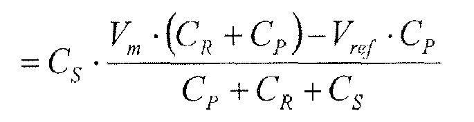
FIGS. 2a to 4b. FIG. 2a shows the interconnection of the sensor capacitor Cp, the reference capacitor CR and the sampling capacitor CS in a first sample phase. Sensor capacitor CP and reference capacitor CR are connected in series with each other. One plate of sensor capacitor CP is connected to a voltage potential Vrefp while one plate of reference capacitor CR is connected to a potential Vrefm. Thus, a reference voltage Vref =Vrefp - Vrefm is divided by a capacitive voltage divider which is formed by the two capacitors CP, CR. The voltage at interconnection node A depends on the ratio between the capacitances of the reference capacitor CR and the sensor capacitor CP. As the capacitance of reference capacitor CR is constant, the voltage at interconnection node A varies with the capacitance change of sensor capacitor Cp. In the sample phase the sampling capacitor CS is connected between the interconnection node A and a potential Vm, so that the sampling capacitor CS is charged depending on the potential at the interconnection node A. The charge QS stored on CS is defined by:
-
FIG. 2b shows the transfer phase which follows the first sample phase when the sampling capacitor CS is charged. The sampling capacitor CS is connected to differential inputs of asampling amplifier 22, which is included on theintegrated readout circuitry 20. In the transfer phase the charge on sampling capacitor CS is transferred to the sampling amplifier. On the differential output terminals ofsampling amplifier 22 appears an output voltage Vout. Each output of thesampling amplifier 22 is looped back to a different one of the differential inputs by a feedback capacitor Cf. The output voltage Vout of thesampling amplifier 22 is proportional to the charge stored on sampling capacitor CS. The output voltage Vout is defined to:
- So far, the sampling and transfer phases have been discussed for ideal circuitry. But the sensor capacitor CP is external to the integrated readout circuit and there are leakage currents. Leakage occurs at both plates of sensor capacitor CP but relevant is only the leakage at the high impedance interconnection node A.
FIG. 3 symbolizes the leakage by a leakage resistor RL through which a leakage current IV passes. IV is the leakage current which occurs through the ESD protection circuit and through parasitic resistor R shown inFIG. 1 . Thus, the charge QS which is stored on sampling capacitor CS is decreased by a charge ΔQ which is transferred by the leakage current IV to ground during the sample phase. When taking this leakage current into consideration the charge QS stored on the sampling capacitor CS at the end of the sample phase is:
- This leakage current leads to the aforementioned measurement errors.
- In the inventive method the capacitive voltage divider is switched on a second time but with a different polarity to cancel out the effect of the leakage current.
FIG. 4a shows the capacitors' configuration during the second sample phase. Sensor capacitor CP and reference capacitor CR are interconnected at interconnection node A. They are connected in series but contrary to sample phase 1 reference capacitor CR is now connected to the potential Vref while sensor capacitor CP is now connected to the voltage potential Vrefm. As in the first sample phase sampling capacitor CS is connected between the interconnection node A and potential Vm and charged. The leakage current IV shown inFIG. 3 always flows to chip ground. As the polarity of the reference voltage is inversed during the second sample phase compared to the first sample phase, the voltage VS over sampling capacitor CS also changes polarity while the leakage current IV does not.FIG. 4b shows the second transfer phase. The plate of sampling capacitor CS which was in the first transfer phase connected to the negative input terminal ofsampling amplifier 22 is now connected to the positive input terminal ofsampling amplifier 22. Thus, the sampling capacitor CS is connected to the inputs of thesampling amplifier 22 with a polarity opposite to this in transfer phase 1. Therefore, the polarity change effectuated in the sample phase is compensated. As the charge in the feedback capacitors Cf is preserved over the two transfer phases, the output voltages of the two transfer phases are averaged which cancels out the effect of the leakage current IV. Connecting the sampling capacitor CS floating to the differential inputs of the amplifier during the transfer phases has the advantage that no precise common mode regulation for the fully differential amplifier is needed. This allows a cheaper implementation of this fully differential amplifier. - Regarding the two sampling and the two transfer phases together leads to the following calculation which demonstrates that the effect of the leakage current IV, is cancelled out.
- During the first sample phase the charge is:

- In the second sample phase the polarity is changed, so the charge is:

- As the feedback capacitors Cf preserve the charge collected during the first transfer phase there is an output voltage at the output terminals of
sampling amplifier 22 which is an addition of the output voltages of the two transfer phases:



- The effect of leakage current is cancelled out; the output voltage only depends on the applied reference voltage Vref and the values of the capacitances of the sampling capacitor CS, reference capacitor CR, sensor capacitor CP and feedback capacitors Cf.
-
FIGS. 5 to 8 show a realization in a preferred embodiment. Voltages Vrefp, Vrefm and Vm are applied to the circuit and a differential output voltage Voutp, Voutm is output. Included are a sampling capacitor CS, a reference capacitor CR, a sensor capacitor CP and feedback capacitors Cf as well as asampling amplifier 22 and a switching arrangement with a plurality of switches which allow change between the different phases.FIG. 5 shows a capacitance-to-voltage converter in a state for the first sample phase. The sampling capacitor CS is connected to an interconnection node of reference capacitor CR and sensor capacitor CS.FIG. 6 shows the capacitance-to-voltage converter in a state for the first transfer phase, the sampling capacitor CS is now disconnected from capacitors CR, CP and connected to the input terminals ofsampling amplifier 22.FIG. 7 shows the capacitance-to-voltage converter in a state for the second sample phase. Compared to the state inFIG. 5 the reference voltage is inversed, sensor capacitor CP is now connected to Vrefp, and reference capacitor CR is now connected to Vrefp.FIG. 8 shows the capacitance-to-voltage converter in a state for the second transfer phase. Compared to the state shown inFIG. 6 the polarity of the sampling capacitor Cs on the input terminals ofsampling amplifier 22 is inversed. - The described inventive capacitance-to-voltage converter delivers a precise measurement even when using a cheap sensor capacitor and with temperatures up to 125°C. Therefore it is advantageously used in a tire pressure monitoring system with a sensor capacitor in a range of about 5 to 20 pF and a capacitance-to-voltage converter for each tire.
Claims (10)
- A method of capacitance-to-voltage conversion with an external sensor capacitor (CP) and a capacitance-to-voltage converter (14) implemented on an integrated readout circuit that includes a reference capacitor (CR), a sampling capacitor (CS) and a sampling amplifier (22) and has input terminals (16) to which the sensor capacitor (CP) is connected, comprising the following sequence of steps:a) applying a reference voltage (Vref) to the series connected sensor capacitor (CP) and reference capacitor (CR) and charging the sampling capacitor (CS) to the potential at the interconnection node (A) between the sensor capacitor (CP) and the reference capacitor (CR);b) connecting the sampling capacitor (CS) to inputs of the sampling amplifier (22);c) applying the reference voltage (Vref) to the series connected sensor capacitor (CP) and reference capacitor (CR) with a polarity opposite to that in step a) and charging the sampling capacitor (CS) to the potential at the interconnection node (A) between the sensor capacitor (CP) and the reference capacitor (CR); andd) connecting the sampling capacitor (CS) to the inputs of the sampling amplifier (22) in a polarity opposite to that in step b).
- The method of Claim 1, wherein steps a) to d) are repeated multiple times.
- The method of Claim 1 or Claim 2, wherein the sampling capacitor (CS) is connected in steps b) and d) to differential inputs of the sampling amplifier (22) and a differential output is generated by the sampling amplifier (22).
- A capacitance-to-voltage converter (14) implemented on an integrated readout circuit for reading out an external sensor capacitor (CP) and including a reference capacitor (CR), a sampling capacitor (CS) and a sampling amplifier (22) and which has input terminals (16) to which the sensor capacitor (CP) is connected, further comprising a switching arrangement which during capacitance-to-voltage conversion carries out the sequence of steps of selectivelya) connecting the series connected sensor capacitor (CP) and reference capacitor (CR) to a reference voltage source and connecting the sampling capacitor (CS) to the interconnection node (A) between the sensor capacitor (CP) and the reference capacitor (CR);b) connecting the sampling capacitor (CS) to inputs of the sampling amplifier (22);c) connecting the series connected sensor capacitor (CP) and reference capacitor (CR) to the reference voltage source with a polarity opposite to that in feature a) and connecting the sampling capacitor (CS) to the interconnection node (A) between the sensor capacitor (CP) and the reference capacitor (CR);d) connecting the sampling capacitor (CS) to the inputs of the sampling amplifier (22) with a polarity opposite to that in feature b).
- The capacitance-to-voltage converter (14) of Claim 4, wherein the sampling amplifier (22) has differential inputs.
- The capacitance-to-voltage converter (14) of Claim 5, wherein each output of the sampling amplifier (22) comprises a feedback loop to a different one of the differential inputs with a feedback capacitor (CF).
- The capacitance-to-voltage converter (14) according to any of Claims 4 to 6, wherein the integrated readout circuit includes ESD protection circuits (18) associated with the input terminals (16).
- The capacitance-to-voltage converter (14) according to any of Claims 4 to 7, wherein the sensor capacitor (CP) is associated with a pneumatic pressure sensor.
- The capacitance-to-voltage converter (14) according to any of Claims 4 to 7, wherein the sensor capacitor (CP) is associated with an acceleration sensor.
- A tire pressure monitoring automotive system including for each tire to be monitored a pressure sensor with a sensor capacitor (CP) and a capacitance-to-voltage converter (14) according to any of Claims 4 to 8, to the input terminals of which the sensor capacitor (CP) is connected.
Applications Claiming Priority (2)
| Application Number | Priority Date | Filing Date | Title |
|---|---|---|---|
| DE102005028507A DE102005028507B3 (en) | 2005-06-17 | 2005-06-17 | Method for capacitance-voltage conversion and capacitance-voltage converter |
| PCT/EP2006/063321 WO2006134176A1 (en) | 2005-06-17 | 2006-06-19 | Capacitance-to-voltage conversion method and apparatus |
Publications (2)
| Publication Number | Publication Date |
|---|---|
| EP1894026A1 EP1894026A1 (en) | 2008-03-05 |
| EP1894026B1 true EP1894026B1 (en) | 2017-05-31 |
Family
ID=36950378
Family Applications (1)
| Application Number | Title | Priority Date | Filing Date |
|---|---|---|---|
| EP06763777.7A Ceased EP1894026B1 (en) | 2005-06-17 | 2006-06-19 | Capacitance-to-voltage conversion method and apparatus |
Country Status (7)
| Country | Link |
|---|---|
| US (1) | US7663379B2 (en) |
| EP (1) | EP1894026B1 (en) |
| JP (1) | JP2008546994A (en) |
| KR (1) | KR20080021143A (en) |
| CN (1) | CN101198876B (en) |
| DE (1) | DE102005028507B3 (en) |
| WO (1) | WO2006134176A1 (en) |
Cited By (1)
| Publication number | Priority date | Publication date | Assignee | Title |
|---|---|---|---|---|
| US11733060B2 (en) | 2021-02-09 | 2023-08-22 | Infineon Technologies Ag | Diagnosis of electrical failures in capacitive sensors |
Families Citing this family (22)
| Publication number | Priority date | Publication date | Assignee | Title |
|---|---|---|---|---|
| TWI402513B (en) * | 2008-08-18 | 2013-07-21 | Raydium Semiconductor Corp | Capacitance evaluation circuit |
| US8125231B2 (en) * | 2009-01-28 | 2012-02-28 | Freescale Semiconductor, Inc. | Capacitance-to-voltage interface circuit, and related operating methods |
| CH700376A2 (en) * | 2009-02-11 | 2010-08-13 | Baumer Innotec Ag | Capacitive sensor and method for capacitive sensing an object distance. |
| EP2795350B1 (en) | 2011-12-23 | 2015-11-25 | Imec | Method and system for measuring capacitance difference between capacitive elements |
| US9164133B2 (en) * | 2012-11-02 | 2015-10-20 | Power Integrations, Inc. | Switched averaging error amplifier |
| US9310269B2 (en) * | 2012-11-30 | 2016-04-12 | Sensata Technologies, Inc. | Analog front-end compensation |
| CN103036511B (en) * | 2012-12-14 | 2015-06-03 | 电子科技大学 | ADC (analog-to-digital converter) allowance amplifying circuit of infrared focal plane array detector readout circuit |
| US9236012B2 (en) * | 2014-05-15 | 2016-01-12 | Himax Technologies Limited | Sensing apparatus of display panel |
| CN104101368B (en) * | 2014-07-07 | 2016-08-17 | 湘潭大学 | Test using capacitance sensor reading circuit based on fully differential switching capacity principle |
| CN105656458A (en) * | 2015-12-28 | 2016-06-08 | 芜湖国睿兆伏电子有限公司 | Discharging automatic inhibit signal generation circuit of capacitor charging power supply |
| US20190067962A1 (en) * | 2016-03-15 | 2019-02-28 | Sanyo Electric Co., Ltd. | Management device and power supply device |
| DE102017209096A1 (en) * | 2017-05-31 | 2018-12-06 | Robert Bosch Gmbh | Evaluation circuit for a capacitive acceleration sensor and device for detecting an acceleration |
| TWI644107B (en) | 2017-11-23 | 2018-12-11 | 財團法人工業技術研究院 | Readout circuit for sensor and readout method therefor |
| US11079881B2 (en) * | 2018-01-10 | 2021-08-03 | Novatek Microelectronics Corp. | Signal processing circuit and system |
| US10901552B2 (en) | 2018-01-10 | 2021-01-26 | Novatek Microelectronics Corp. | Signal processing circuit and related method of processing sensing signal |
| CN110598515B (en) * | 2018-06-13 | 2023-12-26 | 联咏科技股份有限公司 | Signal processing circuit and system |
| CN109669054B (en) * | 2019-02-20 | 2021-01-05 | 哈尔滨工程大学 | A High Precision Fully Differential Capacitance-Voltage Conversion Circuit System |
| US10873299B2 (en) | 2019-03-27 | 2020-12-22 | Intel Corporation | Trans-impedance amplifier transfer function compensation |
| CN113452368B (en) * | 2021-07-15 | 2022-06-10 | 上海芯问科技有限公司 | Capacitance-voltage conversion circuit and application system |
| CN116380135B (en) * | 2023-06-06 | 2023-08-11 | 成都市晶蓉微电子有限公司 | Charge transfer balance type capacitor-to-voltage conversion circuit |
| CN116545428B (en) * | 2023-07-05 | 2023-09-26 | 成都市晶蓉微电子有限公司 | High-precision capacitance-to-voltage conversion error trimming circuit and method |
| CN119356460A (en) * | 2024-10-24 | 2025-01-24 | 中山大学·深圳 | A low power pseudo-continuous capacitance-voltage conversion circuit |
Family Cites Families (16)
| Publication number | Priority date | Publication date | Assignee | Title |
|---|---|---|---|---|
| US577802A (en) * | 1897-02-23 | Gustaf m | ||
| US4054833A (en) * | 1976-06-11 | 1977-10-18 | Setra Systems, Inc. | Capacitance measuring system |
| US4149231A (en) * | 1977-05-04 | 1979-04-10 | Bunker Ramo Corporation | Capacitance-to-voltage transformation circuit |
| US4404481A (en) * | 1980-10-20 | 1983-09-13 | Matsushita Electric Industrial Co., Ltd. | Capacitance to voltage conversion apparatus |
| JP3125675B2 (en) * | 1996-03-29 | 2001-01-22 | 三菱電機株式会社 | Capacitive sensor interface circuit |
| US5770802A (en) * | 1997-04-16 | 1998-06-23 | Texas Instruments Incorporated | Sensor with improved capacitive to voltage converter integrated circuit |
| US20010020850A1 (en) * | 1998-03-10 | 2001-09-13 | Mcintosh Robert B. | Capacitance measurement circuit with digital output |
| JP2000065664A (en) * | 1998-08-26 | 2000-03-03 | Hitachi Ltd | Capacitance type dynamic quantity sensor |
| CN2411482Y (en) * | 1999-04-23 | 2000-12-20 | 浙江大学 | Procedure chromatographic analysis imaging device base on capacitance sensor |
| JP4352562B2 (en) * | 2000-03-02 | 2009-10-28 | 株式会社デンソー | Signal processing device |
| DE10010888B4 (en) * | 2000-03-06 | 2004-02-12 | Infineon Technologies Ag | Circuit arrangement and method for evaluating capacities in matrices |
| US20040004488A1 (en) * | 2002-07-02 | 2004-01-08 | Baxter Larry K. | Capacitive sensor circuit with good noise rejection |
| US7129714B2 (en) * | 2002-07-02 | 2006-10-31 | Baxter Larry K | Capacitive measurement system |
| US6768319B2 (en) * | 2002-07-10 | 2004-07-27 | Rosemount Inc. | Adaptive compensation of measurement error for industrial process control transmitters |
| JP4036798B2 (en) * | 2003-07-29 | 2008-01-23 | アルプス電気株式会社 | Capacitance detection circuit, detection method, and fingerprint sensor |
| JP2005140657A (en) * | 2003-11-07 | 2005-06-02 | Denso Corp | Capacitance sensor capacitance change detection circuit |
-
2005
- 2005-06-17 DE DE102005028507A patent/DE102005028507B3/en not_active Expired - Fee Related
-
2006
- 2006-06-19 CN CN2006800214061A patent/CN101198876B/en not_active Expired - Fee Related
- 2006-06-19 WO PCT/EP2006/063321 patent/WO2006134176A1/en not_active Ceased
- 2006-06-19 JP JP2008516341A patent/JP2008546994A/en not_active Abandoned
- 2006-06-19 EP EP06763777.7A patent/EP1894026B1/en not_active Ceased
- 2006-06-19 US US11/425,013 patent/US7663379B2/en active Active
- 2006-06-19 KR KR1020087001237A patent/KR20080021143A/en not_active Ceased
Cited By (1)
| Publication number | Priority date | Publication date | Assignee | Title |
|---|---|---|---|---|
| US11733060B2 (en) | 2021-02-09 | 2023-08-22 | Infineon Technologies Ag | Diagnosis of electrical failures in capacitive sensors |
Also Published As
| Publication number | Publication date |
|---|---|
| JP2008546994A (en) | 2008-12-25 |
| DE102005028507B3 (en) | 2006-11-30 |
| US7663379B2 (en) | 2010-02-16 |
| KR20080021143A (en) | 2008-03-06 |
| CN101198876B (en) | 2010-09-29 |
| EP1894026A1 (en) | 2008-03-05 |
| WO2006134176A1 (en) | 2006-12-21 |
| US20060284603A1 (en) | 2006-12-21 |
| CN101198876A (en) | 2008-06-11 |
Similar Documents
| Publication | Publication Date | Title |
|---|---|---|
| US7663379B2 (en) | Capacitance-to-voltage conversion method and apparatus | |
| EP0975983B1 (en) | Capacitance detection system and method | |
| EP2751579B1 (en) | Linear capacitance-to-voltage converter using a single amplifier for transducer front ends with cancellation of spurious forces contributed by sensor circuitry | |
| CN103890593B (en) | Strengthen by using the linearity of neutralizing capacitor and the linear activated capacitive transducer of calibration automatically on sheet | |
| US10564186B2 (en) | Current sense amplifier architecture and level shifter | |
| US8508217B2 (en) | Output circuit of charge mode sensor | |
| US10768020B2 (en) | Capacitive sensor | |
| US10088497B2 (en) | Acceleration sensor | |
| US6357298B1 (en) | Micromechanical sensor and method for operating the sensor | |
| KR20150058403A (en) | Capacitance measurement of high voltage device | |
| EP0835453B1 (en) | Ratiometric circuit | |
| US20060162454A1 (en) | Capacitive acceleration sensor arrangement | |
| US7055387B2 (en) | Apparatus for and method of sensing a measured input | |
| JP4069158B1 (en) | Charge amplifier, charge amplifier device, and bias current compensation method | |
| US7112950B2 (en) | Integrated circuit for use with an external hall sensor, and hall sensor module | |
| JP2017096886A (en) | Piezoelectric sensor | |
| KR100738692B1 (en) | Potential holding device, capacity measuring device and potential fixing method | |
| KR100296979B1 (en) | Sensor circuit | |
| US8030915B2 (en) | Integrated sensor with capacitive coupling rejection to the mechanical ground | |
| CN108982991B (en) | Evaluation circuit for a capacitive acceleration sensor and device for detecting acceleration | |
| Custodio et al. | A novel sensor-bridge-to-microcontroller interface | |
| JPH11132787A (en) | Electric quantity detection circuit |
Legal Events
| Date | Code | Title | Description |
|---|---|---|---|
| PUAI | Public reference made under article 153(3) epc to a published international application that has entered the european phase |
Free format text: ORIGINAL CODE: 0009012 |
|
| 17P | Request for examination filed |
Effective date: 20080117 |
|
| AK | Designated contracting states |
Kind code of ref document: A1 Designated state(s): DE FR GB |
|
| DAX | Request for extension of the european patent (deleted) | ||
| RBV | Designated contracting states (corrected) |
Designated state(s): DE FR GB |
|
| DAX | Request for extension of the european patent (deleted) | ||
| GRAP | Despatch of communication of intention to grant a patent |
Free format text: ORIGINAL CODE: EPIDOSNIGR1 |
|
| INTG | Intention to grant announced |
Effective date: 20161222 |
|
| GRAS | Grant fee paid |
Free format text: ORIGINAL CODE: EPIDOSNIGR3 |
|
| GRAA | (expected) grant |
Free format text: ORIGINAL CODE: 0009210 |
|
| AK | Designated contracting states |
Kind code of ref document: B1 Designated state(s): DE FR GB |
|
| REG | Reference to a national code |
Ref country code: GB Ref legal event code: FG4D |
|
| REG | Reference to a national code |
Ref country code: FR Ref legal event code: PLFP Year of fee payment: 12 |
|
| REG | Reference to a national code |
Ref country code: DE Ref legal event code: R096 Ref document number: 602006052686 Country of ref document: DE |
|
| REG | Reference to a national code |
Ref country code: DE Ref legal event code: R097 Ref document number: 602006052686 Country of ref document: DE |
|
| PLBE | No opposition filed within time limit |
Free format text: ORIGINAL CODE: 0009261 |
|
| STAA | Information on the status of an ep patent application or granted ep patent |
Free format text: STATUS: NO OPPOSITION FILED WITHIN TIME LIMIT |
|
| 26N | No opposition filed |
Effective date: 20180301 |
|
| REG | Reference to a national code |
Ref country code: FR Ref legal event code: PLFP Year of fee payment: 13 |
|
| PGFP | Annual fee paid to national office [announced via postgrant information from national office to epo] |
Ref country code: DE Payment date: 20210519 Year of fee payment: 16 Ref country code: FR Payment date: 20210519 Year of fee payment: 16 |
|
| PGFP | Annual fee paid to national office [announced via postgrant information from national office to epo] |
Ref country code: GB Payment date: 20210519 Year of fee payment: 16 |
|
| REG | Reference to a national code |
Ref country code: DE Ref legal event code: R119 Ref document number: 602006052686 Country of ref document: DE |
|
| GBPC | Gb: european patent ceased through non-payment of renewal fee |
Effective date: 20220619 |
|
| PG25 | Lapsed in a contracting state [announced via postgrant information from national office to epo] |
Ref country code: FR Free format text: LAPSE BECAUSE OF NON-PAYMENT OF DUE FEES Effective date: 20220630 |
|
| PG25 | Lapsed in a contracting state [announced via postgrant information from national office to epo] |
Ref country code: GB Free format text: LAPSE BECAUSE OF NON-PAYMENT OF DUE FEES Effective date: 20220619 Ref country code: DE Free format text: LAPSE BECAUSE OF NON-PAYMENT OF DUE FEES Effective date: 20230103 |