EP1890478A2 - Image pickup apparatus, defect compensation device, and defect-compensating method - Google Patents
Image pickup apparatus, defect compensation device, and defect-compensating method Download PDFInfo
- Publication number
- EP1890478A2 EP1890478A2 EP07253162A EP07253162A EP1890478A2 EP 1890478 A2 EP1890478 A2 EP 1890478A2 EP 07253162 A EP07253162 A EP 07253162A EP 07253162 A EP07253162 A EP 07253162A EP 1890478 A2 EP1890478 A2 EP 1890478A2
- Authority
- EP
- European Patent Office
- Prior art keywords
- signal
- compensation
- pixel
- defect
- defective pixel
- Prior art date
- Legal status (The legal status is an assumption and is not a legal conclusion. Google has not performed a legal analysis and makes no representation as to the accuracy of the status listed.)
- Withdrawn
Links
Images



Classifications
-
- H—ELECTRICITY
- H04—ELECTRIC COMMUNICATION TECHNIQUE
- H04N—PICTORIAL COMMUNICATION, e.g. TELEVISION
- H04N25/00—Circuitry of solid-state image sensors [SSIS]; Control thereof
- H04N25/60—Noise processing, e.g. detecting, correcting, reducing or removing noise
- H04N25/68—Noise processing, e.g. detecting, correcting, reducing or removing noise applied to defects
- H04N25/683—Noise processing, e.g. detecting, correcting, reducing or removing noise applied to defects by defect estimation performed on the scene signal, e.g. real time or on the fly detection
-
- H—ELECTRICITY
- H04—ELECTRIC COMMUNICATION TECHNIQUE
- H04N—PICTORIAL COMMUNICATION, e.g. TELEVISION
- H04N23/00—Cameras or camera modules comprising electronic image sensors; Control thereof
- H04N23/80—Camera processing pipelines; Components thereof
- H04N23/84—Camera processing pipelines; Components thereof for processing colour signals
-
- H—ELECTRICITY
- H04—ELECTRIC COMMUNICATION TECHNIQUE
- H04N—PICTORIAL COMMUNICATION, e.g. TELEVISION
- H04N25/00—Circuitry of solid-state image sensors [SSIS]; Control thereof
- H04N25/60—Noise processing, e.g. detecting, correcting, reducing or removing noise
- H04N25/68—Noise processing, e.g. detecting, correcting, reducing or removing noise applied to defects
Definitions
- a signal level of the pixel signal relative to a defective pixel may be compensated to a different signal level from the signal level of the image signal constituted of only signal component by the incident beam, thereby resulting in deterioration in reliability of the defect compensation.
- the compensation signal is generated for each defective pixel based on the offset of the pixel signal relative to the defective pixel indicated by the defect information relative to the defective pixel in the image pickup element, which results in the offset of the pixel signal generated for each pixel.
- the first signal obtained by compensation of the pixel signal- relative to the defective pixel with using the compensation signal and the second signal obtained by compensation of the pixel signal relative to the defective pixel without using the compensation signal are switched based on a comparison result of a signal level of the compensation signal with a signal level of a predetermined compensation-switching reference signal.
- the switched signal is set as an image signal in which the pixel signal relative to the defective pixel is compensated.
- a defect compensation section 31 in the image-signal-processing device 30 performs any defect compensation on the image signals DRa, DGa, DBa of the three primary colors received from the image pickup device 20 to compensate for a signal level of a pixel signal relative to any defective pixel(s) so that the defective pixel(s) can be inconspicuous.
- the defect compensation section 31 then generates image signals DRb, DGb, DBb and supplies a level adjustment section 32 with these compensated image signals DRb, DGb, DBb.
- the defect-compensation-processing part 31R when a signal relative to the first defective pixel is supplied to the defect-compensation-processing part 31R, the data indicating an amount of offset thereof is supplied to the defect-compensation-processing part 31R as the defect information RPR Alternatively, when a signal relative to the second defective pixel is supplied to the defect-compensation-processing part 31R, the data, which is peculiar to the second defective pixel, indicating the second defective pixel is supplied to the defect-compensation-processing part 31R as the defect information RPR
- the second compensation unit 314 compensates for the pixel signal relative to the first defective pixel(s) without using the compensation signal, so that any over-compensation-free defect compensation can be performed.
- An image signal DRa is supplied to both of the first and second compensation units 312, 314 in the defect-compensation-processing part 131R
- the first compensation unit 312 performs any compensation on the image signal DRa so that a pixel signal relative to the first defective pixel(s) can be compensated.
- the first compensation unit 312 then generates a compensated image signal DRah and supplies a fixed terminal Pa of a signal changeover switch 315 with the compensated image signal DRah.
- the second compensation unit 314 performs any compensation on the image signal DRa so that the pixel signal relative to the second defective pixel(s) can be compensated.
Landscapes
- Engineering & Computer Science (AREA)
- Multimedia (AREA)
- Signal Processing (AREA)
- Transforming Light Signals Into Electric Signals (AREA)
Abstract
Description
- The present invention relates to an image pickup apparatus, and a defect compensation device and a defect-compensating method, which are used in the image pickup apparatus.
- In image pickup elements such as a charge coupled devices (CCD) image sensor or a complementary metal-oxide semiconductor (CMOS) image sensor, a plurality of pixels each for performing photoelectric conversion is provided. An image signal is generated based on a pixel signal that is generated by each of the pixels. In such the image pickup elements, there may be a defective pixel (hereinafter, referred to as "first defective pixel'') in which the pixel signal generated for each pixel results in a greater amount of offset than a level that has been previously set because of lack of uniformity on the element's characteristic. Further, there may be another defective pixel (hereinafter, referred to as "second defective pixel'') in which the pixel signal generated for each pixel results in a signal having a level that is independent on an incident beam because of a lattice defect thereof and the like. Accordingly, in an image pickup apparatus equipped with such the image pickup element, in order to prevent any picture quality from being made poor by these defective pixels, any defect compensation to compensate for a pixel signal corresponding to each of these defective pixels is performed in the image signal so that these defective pixels can be very little visible in an image.
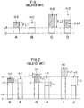
- In a case of the defect compensation of the pixel signal relative to the first defective pixel, an amount of the offset of the pixel signal relative to the first defective pixel is deleted from the pixel signal by using the compensation signal corresponding to the offset of the pixel signal relative to the first defective pixel. For example, if the pixel signal relative to the first defective pixel results in an offset OS of the pixel signal A (illustrated by oblique lines in FIG. 1) generated by the image pickup element, the offset OS can be deleted from the pixel signal A by subtracting a compensation signal HC having a same level as an amount of offset FL1 of the offset OS from the pixel signal A so that a pixel signal B shown in FIG. 1 can be generated. If, however, the offset OS of the pixel signal relative to the first defective pixel increases from the amount of offset FL1 to an amount of offset FL2 as a pixel signal C shown in FIG. 1 based on any fluctuation in temperature characteristic of the image pickup element, an offset OSR remains in a pixel signal D shown in FIG. 1 even when subtracting the compensation signal HC having the same level as an amount of offset FL1 of the offset OS from the pixel signal C. It is to be noted that signal levels LB shown in FIG. 1 and FIG. 2, which will be described in later, indicate a black level.
-
Japanese Patent No. 3104098 Japanese Patent No. 3104098 Japanese Patent Application Publication No. H06-113211 - The image pickup apparatus has video amplifier(s) for amplifying an image signal output from image pickup elements, in order to be able to acquire an image signal having a desired signal level even under low-luminous intensity. When setting gain of the video amplifier(s) to a higher level in addition to the increase in the amount of the offset based on any fluctuation in the temperature characteristics of the image pickup element, it is difficult to perform any higher accurate defect compensation if a signal level of the compensation signal is also increased.
- If, however, the signal level of the compensation signal is increased, it may be easy to result in over-compensation and be obviously influenced by this over-compensation. For example, when a pixel signal E shown in FIG. 2 has a small amount of the offset OS (i.e., when the compensation signal HC has a low signal level), it is possible to perform any defect compensation on the pixel signal E until the signal level of the pixel signal E reaches its saturation level LS so that a compensated pixel signal F shown in FIG. 2 can be acquired. It is to be noted that a signal level LC is a signal level when no offset result in a pixel signal. If any defect compensation is performed on a pixel signal G shown in FIG. 2 when its offset OS has a larger amount of the offset FL2 than the amount of the offset FL1 of the pixel signal E, this results in over-compensation by subtracting the compensation signal HC having the amount FL2 of the offset from the saturation level LS of the pixel signal G, so that a pixel signal H, shown in FIG. 2, having a signal level that is less than the signal level LC by an amount of offset FLv, which exceeds the saturation level LS in the pixel signal G, can be acquired. Further, If any defect compensation is performed on a pixel signal I shown in FIG. 2 when the signal level of the image signal I excluding the offset exceeds its saturation level LS, a pixel signal J shown in FIG. 2 having a level that is less than the saturation level LS by an amount of offset FL2, which exceeds the saturation level LS in the pixel signal I, can be acquired. Thus, the signal level of the compensated pixel signal J is very different from a signal level of the pixel that has no offset, so that the compensated pixel signal J can be obviously influenced by the over-compensation.
- If there is a large amount of an offset, a signal component of the offset is predominant in the image signal as compared with a signal component by incident beam. Accordingly, it is difficult to compensate for a pixel signal to generate an image signal constituted of only signal component by the incident beam unless the offset is deleted with a high accuracy. Namely, if the compensation signal has a lower signal level than that of the image signal constituted of only signal component by the incident beam, even when a compensation signal contains any errors, any influence by the errors may be ignored. If, however, the compensation signal has a higher signal level than that of the image signal constituted of only signal component by the incident beam, it is difficult for any influence by the errors contained in the compensation signal to be ignored. If the image signal constituted of only signal component by the incident beam has a lower signal level than that of any errors contained in the compensation signal so that a subject is imaged under low luminous intensity, a signal level of the pixel signal relative to a defective pixel may be compensated to a different signal level from the signal level of the image signal constituted of only signal component by the incident beam, thereby resulting in deterioration in reliability of the defect compensation.
- It is desirable to provide an image pickup apparatus, a defect compensation device, and defect-compensating method, which are capable of performing the defect compensation satisfactorily.
- Various respective aspects and features of the invention are defined in the appended claims. Combinations of features from the dependent claims may be combined with features of the independent claims as appropriate and not merely as explicitly set out in the claims.
- According to an embodiment of the present invention, there is provided an image pickup apparatus. The image pickup apparatus includes an image pickup device that contains an image pickup element The image pickup device generates an image signal by using the image pickup element The image pickup apparatus also has a defect-information-storing unit that stores defect information relative to a defective pixel in the image pickup element The defective pixel results in an offset of a pixel signal generated for each pixel. The offset has a larger amount thereof than a predetermined amount The image pickup apparatus further has a compensation-signal-generating unit that generates a compensation signal for each defective pixel based on the offset of the pixel signal relative to the defective pixel indicated by the defect information. The image pickup apparatus additionally has a first compensation unit that compensates for the pixel signal relative to the defective pixel indicated by the defect information with applying the compensation signal to the pixel signal and a second compensation unit that compensates for the pixel signal relative to the defective pixel indicated by the defect information without applying the compensation signal to the pixel signal. The image pickup apparatus still further has a compensation-switching unit that switches between a first signal compensated by the first compensation unit and a second signal compensated by the second compensation unit based on a comparison result of a signal level of the compensation signal with a signal level of a predetermined compensation-switching reference signal and sets the switched signal as the image signal in which the pixel signal relative to the defective pixel is compensated.
- According to another embodiment of the invention, there is provided a defect compensation device. The defect compensation device also includes a defect-information-storing unit that stores defect information relative to a defective pixel that results in an offset of a pixel signal. The offset has a larger amount thereof than a predetermined amount The defect compensation device includes a compensation-signal-generating unit that generates a compensation signal for each defective pixel based on the offset of the pixel signal relative to the defective pixel indicated by the defect information. The defect compensation device further includes a first compensation unit that compensates for the pixel signal relative to the defective pixel indicated by the defect information with applying the compensation signal to the pixel signal and a second compensation unit that compensates for the pixel signal relative to the defective pixel indicated by the defect information without applying the compensation signal to the image signal. The defect compensation device additionally includes a compensation-switching unit that switches between a first signal compensated by the first compensation unit and a second signal compensated by the second compensation unit based on a comparison result of a signal level of the compensation signal with a signal level of a predetermined compensation-switching reference signal and sets the switched signal as an image signal in which the pixel signal relative to the defective pixel is compensated.
- According to further embodiment of the invention, there is provided a defect-compensating method that compensates for a pixel signal relative to a defective pixel in an image pickup element, which results in a larger offset of the pixel signal generated by the image pickup element for each pixel than a predetermined value by using defect information relative to the defective pixel, to obtain an image signal in which the pixel signal relative to the defective pixel is compensated. The method contains a compensation-signal-generating step of generating a compensation signal for each defective pixel based on the offset of the pixel signal relative to the defective pixel indicated by the defect information. The method also contains a first compensating step of compensating for the pixel signal relative to the defective pixel indicated by the defect information with applying the compensation signal to the pixel signal generated by the image pickup element and a second compensating step of compensating for the pixel signal relative to the defective pixel indicated by the defect information without applying the compensation signal to the pixel signal generated by the image pickup element The method further contains a compensation-switching step of switching between a first signal compensated in the first compensating step and a second signal compensated by the second compensating step based on a comparison result of a signal level of the compensation signal with a signal level of a predetermined compensation-switching reference signal and setting the switched signal as the image signal in which the pixel signal relative to the defective pixel is compensated.
- In the above embodiments, the compensation signal is generated for each defective pixel based on the offset of the pixel signal relative to the defective pixel indicated by the defect information relative to the defective pixel in the image pickup element, which results in the offset of the pixel signal generated for each pixel. The first signal obtained by compensation of the pixel signal- relative to the defective pixel with using the compensation signal and the second signal obtained by compensation of the pixel signal relative to the defective pixel without using the compensation signal are switched based on a comparison result of a signal level of the compensation signal with a signal level of a predetermined compensation-switching reference signal. The switched signal is set as an image signal in which the pixel signal relative to the defective pixel is compensated.
- It is to be noted that the defect information is referred to information that is used to compensate for a pixel signal relative to a defective pixel or defective pixels that results or result in the offset having a larger amount thereof than a predetermined level. The defect information contains a location of the defective pixel(s) and an amount of its (their) offset It is also to be noted that the compensation is referred to any compensation of a pixel signal relative to defective pixel(s) and includes replacement of compensation generating any over-compensation with another and concealment of the compensation generating any over-compensation from another.
- When the pixel signal relative to the defective pixel is compensated by using the compensation signal, the compensation signal is added or subtracted to or from the pixel signal relative to the defective pixel(s), which is generated by using the image pickup element, indicated by the defect information so that the offset of the pixel signal relative to the defective pixel indicated by the defect information can be deleted from the pixel signal.
- When the pixel signal relative to the defective pixel is compensated by using no compensation signal, the pixel signal relative to the defective pixel having a signal level of the pixel signal generated for each pixel, which is independent on any incident beam, is compensated by using, for example, the fourth signal of peripheral pixels around the defective pixel. The compensation signal compensates for the signal level of the pixel signal based on temperature of the image pickup element and a gain when the image pickup device generates the pixel signal.
- If a signal level of the compensation signal does not exceed a signal level of the predetermined compensation-switching reference signal, the first signal obtained by the compensation of the pixel signal relative to the defective pixel with using the compensation signal is set as the image signal in which the pixel signal relative to the defective pixel is compensated. If a signal level of the compensation signal exceeds a signal level of the predetermined compensation-switching reference signal, the second signal obtained by the compensation of the pixel signal relative to the defective pixel without using the compensation signal is set as the image signal in which the pixel signal relative to the defective pixel is compensated.
- Thus, when the signal level of the compensation signal exceeds a signal level of the predetermined compensation-switching reference signal so that any over-compensation can occur, the second signal obtained by the compensation of the pixel signal relative to the defective pixel without using the compensation signal is set as the image signal in which the pixel signal relative to the defective pixel is compensated. This prevents the over-compensation from occurring, thereby enabling any defect compensation to be suitably performed.
- Embodiments of the invention will now be described with reference to the accompanying drawings, throughout which like parts are referred to by like references, and in which:
- FIG. 1 is a diagram for illustrating an operation for a defect compensation relative to related art;
- FIG. 2 is a diagram for illustrating an over-compensation in the defect compensation operation;
- FIG. 3 is a block diagram for showing a configuration of an embodiment of an image pickup apparatus;
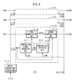
- FIG. 4 is a block diagram for showing a configuration of an embodiment of a defect compensation section;
- FIG. 5 is a block diagram for showing a configuration of another embodiment of the defect compensation section; and
- FIG. 6 is a block diagram for showing a configuration of further embodiment of the defect compensation section.
- The following will describe embodiments of the present invention with reference to the accompanied drawings.
- FIG. 3 shows a configuration of an embodiment of an
image pickup apparatus 10, to which a defect compensation device that compensates for a pixel signal relative to defective pixel(s) in the image pickup element is applied. It is to be noted that in FIG. 3, 3-chipsimage pickup apparatus 10 is shown in which an incident beam of a subject that is incident through an optical system, not shown, constituted of lens, iris or the like is separated into three primary colors by a color separation prism so that the separated beams are incident on each of the image pickup elements provided for the primary colors. - An
image pickup device 20 in theimage pickup apparatus 10 containsimage pickup elements video amplifiers converters 23R, 23G and 23B. - The
image pickup element 21R is constituted of a plurality of pixels each for performing photoelectric conversion. In theimage pickup element 21R, each pixel generates a pixel signal based on red component of the beam separated by the color separation prism. Theimage pickup element 21R generates an image signal SR based on the pixel signal and supplies thevideo amplifier 22R with such the image signal SR. - The
video amplifier 22R receives and amplifies the image signal SR to generate an image signal SRa with its gain being changed based on the gain-changing signal GC received from acontrol section 50, which will be described later. Thevideo amplifier 22R then supplies the A/D converter 23R with the amplified image signal SRa. For example, even when imaging a subject under low-luminous intensity, it is possible to generate the image signal SRa having a desired signal level by increasing a gain in thevideo amplifier 22R based on the gain-changing signal GC. When imaging a subject under satisfactory luminous intensity, thevideo amplifier 22R supplies the A/D converter 23R with the image signal SR as the amplified image signal SRa. - The A/
D converter 23R receives the image signal SRa from thevideo amplifier 22R and converts it to a digital image signal DRa. The A/D converter 23R then supplies the image-signal-processingdevice 30 with the digital image signal DRa. - The
image pickup elements 21G, 21B are respectively constituted of a plurality of pixels each for performing photoelectric conversion, similar to theimage pickup element 21R. In theimage pickup element 21G, each pixel generates a pixel signal based on green component of the beam separated by the color separation prism. Theimage pickup element 21G generates an image signal SG based on the pixel signal and supplies the video amplifier 22G with such the image signal SG. - In the image pickup element 21B, each pixel generates a pixel signal based on blue component of the beam separated by the color separation prism. The image pickup element 21B generates an image signal SB based on the pixel signal and supplies the
video amplifier 22B with such the image signal SB. - The
video amplifiers 22G, 22B respectively have same configurations as that of thevideo amplifier 22R The video amplifier 22G receives and amplifies the image signal SG to generate an image signal SGa with its gain being changed based on the gain-changing signal GC received from thecontrol section 50, which will be described later. The video amplifier 22G then supplies the A/D converter 23G with the amplified image signal SGa. - The
video amplifier 22B receives and amplifies the image signal SB to generate an image signal SBa with its gain being changed based on the gain-changing signal GC received from thecontrol section 50, which will be described later. Thevideo amplifier 22B then supplies the A/D converter 23B with the amplified image signal SBa - The A/D converter 23G receives the image signal SGa from the video amplifier 22G and converts it to a digital image signal DGa. The A/
D converter 23R then supplies the image-signal-processingdevice 30 with the digital image signal DGa. - The A/D converter 23B receives the image signal SBa from the
video amplifier 22B and converts it to a digital image signal DBa. The A/D converter 23B then supplies the image-signal-processingdevice 30 with the digital image signal DBa. - The
image pickup device 20 is also provided with a temperature sensor 24R for detecting temperature of theimage pickup element 21R, atemperature sensor 24G for detecting temperature of theimage pickup element 21G, and a temperature sensor 24B for detecting temperature of the image pickup element 21B. The temperature sensor 24R detects temperature of theimage pickup element 21R and generates a sensor signal TPR indicating the detected temperature. The temperature sensor 24R then supplies thecontrol section 50, which will be described later, with the sensor signal TPR. Similarly, thetemperature sensors 24G, 24B detect temperature of theimage pickup elements 21G, 21B, respectively, and generate sensor signals TPG, TPB indicating the detected temperatures. Thetemperature sensors 24G, 24B then supply thecontrol section 50, which will be described later, with the sensor signals TPG, TRB, respectively. - It is to be noted that, base on a timing signal SYG received from a timing-signal-generating
section 40, which will be described later, and a control signal CT received from thecontrol section 50, theimage pickup elements D converters 23R, 23G, 23B perform A/D conversion processing. - A
defect compensation section 31 in the image-signal-processingdevice 30 performs any defect compensation on the image signals DRa, DGa, DBa of the three primary colors received from theimage pickup device 20 to compensate for a signal level of a pixel signal relative to any defective pixel(s) so that the defective pixel(s) can be inconspicuous. Thedefect compensation section 31 then generates image signals DRb, DGb, DBb and supplies alevel adjustment section 32 with these compensated image signals DRb, DGb, DBb. - The
level adjustment section 32 receives the image signals DRb, DGb, DBb and performs a black level adjustment on them to adjust a black level to hold its fluctuation by dark current on the image signals DRb, DGb, DBb. Thelevel adjustment section 32 also performs a white level adjustment and the like on the image signals DRb, DGb, DBb to adjust their dynamic ranges. Thelevel adjustment section 32 then generates image signals DRc, DGc, DBc and supplies a linear-matrix-processing section 33 with the adjusted image signals DRc, DGc, DBc. - The linear-matrix-
processing section 33 receives the image signals DRc, DGc, DBc and performs any matrix operation on the image signals DRc, DGc, DBc using a predetermined matrix constant, in order to improve color reproducibility, to generate image signals DRd, DGd, DBd as its operation results. The linear-matrix-processing section 33 then supplies aKnee compensation section 34 with the image signals DRd, DGd, DBd. - The
Knee compensation section 34 receives the image signals DRd, DGd, DBd and performs any compression processing on the image signals DRd, DGd, DBd to compress their high-luminance components so that the image signals DRe, DGe, DBe can be generated. TheKnee compensation section 34 then supplies agamma compensation section 35 with the image signals DRe, DGe, DBe. - The
gamma compensation section 35 receives the image signals DRe, DGe, DBe and performs any nonlinear compensation on the image signals DRe, DGe, DBe, in order to establish their true gradation representations when displaying a shot image, to generate nonlinear-compensated image signals DRf, DGf, DBf. Thegamma compensation section 35 then supplies anoutput section 36 with the image signals DRf; DGf, DBf. - The
output section 36 receives the image signals DRf, DGf, DBf and generates an output signal Vout having a predetermined format from the image signals DRf, DGf, DBf and outputs it For example, theoutput section 36 generates a composite signal from the image signals DRf, DGf, DBf and outputs it Theoutput section 36 also generates a luminance signal and a color-difference signal from the image signals DRf, DGf, DBf and outputs them as the output signal V out - The image-signal-processing
device 30 also performs any detail processing or the like to enhance a profile of the shot image. In the image-signal-processingdevice 30, each processing is in synchronism with any image signals by using the timing signals SYG received from the timing-signal-generatingsection 40. - The timing-signal-generating
section 40 generates the timing signal SYG constituted of a clock signal, a horizontal synchronization signal, a vertical synchronization signal and the like. The timing-signal-generatingsection 40 then supplies theimage pickup device 20, the image-signal-processingdevice 30, and thecontrol section 50 with the timing signal SYG. - The
control section 50 is connected with a user interface section 51. The user interface section 51 contains an interface for connecting any external equipment such as a camera control unit and an operation switch that a user manipulates. The user interface section 51 also supplies thecontrol section 50 with an operation signal US such as a signal that is supplied from the external equipment to control operations of theimage pickup apparatus 10 and a signal generated when the user manipulates the switch. - The
control section 50 generates a control signal CT based on the operation signal US and supplies theimage pickup device 20 and the image-signal-processingdevice 30 with the control signal CT to control the operations of theimage pickup apparatus 10 so that theimage pickup apparatus 10 can operate according to any instructions from the external equipment or any user's switch manipulations. - The
control section 50 also generates an offset adjustment signal OG based on the sensor signals TPR, TPG, TPB received from thetemperature sensors 24R, 24G, 24B and the gains of thevideo amplifiers defect compensation section 31. Thecontrol section 50 then supplies thedefect compensation section 31 with the offset adjustment signal OG. Thecontrol section 50 further generates a compensation-switching reference signal CR that is a reference signal for switching the defect-compensating methods based on a signal level of the compensation signal generated according to an offset of a pixel signal relative to the defective pixel(s), which will be described later. Thecontrol section 50 then supplies thedefect compensation section 31 with the compensation-switching reference signal CR - FIG. 4 shows a configuration of the
defect compensation section 31 as an embodiment of a defect compensation device. Thedefect compensation section 31 contains defect-compensation-processing parts processing part 31G performs any defect compensation on the image signal DGa generated based on the green component of the beam. The defect-compensation-processing part 3 1 B performs any defect compensation on the image signal DBa generated based on the blue component of the beam. Thedefect compensation section 31 also contains a defect-information-storingunit 310 that stores defect information relative to the defective pixels in the image pickup elements. - The defect-compensation-
processing parts processing parts - The defect-information-storing
unit 310 is constituted of a nonvolatile memory and a memory controller, both not shown. The nonvolatile memory stores the defect information relative to the first defective pixel in which the pixel signal, which is generated for each pixel, relative to the defective pixel in theimage pickup element 21R results in a greater offset than a level that has been previously set. The nonvolatile memory also stores the defect information relative to the second defective pixel in which the pixel signal relative to the defective pixel results in a signal having a level that is independent on an incident beam. The memory controller supplies the defect-compensation-processing part 31R with the above-mentioned defect information with it being in synchronism with the image signal DRa supplied to the defect-compensation-processing part 31R by utilizing the timing signal SYG received from the timing-signal-generatingsection 40. - This defect information contains information relative to a location and an amount of offset of the first defective pixel(s) and a location of the second defective pixel(s). If it is supposed that each of the pixels in the image pickup element corresponds to any memory address, each of the pieces of the defect information can be stored in a memory address corresponding to the defective pixel. For example, if the defective pixel is the first defective pixel, data indicating an amount of offset thereof is stored in a memory address corresponding to this first defective pixel. If the defective pixel is the second defective pixel, data peculiar to the second defective pixel, which is not used as the data for the first defective pixel, is stored in a memory address corresponding to this second defective pixel.
- Thus, if each pixel corresponds to a memory address, the
image pickup element 21R transmits the pixel signal in order to generate the image signal SR and the memory controller in the defect-information-storingunit 310 reads the data out of its nonvolatile memory with, for example, a memory address being incremented for each reading of the pixel signal based on the timing signal SYG, thereby enabling the defect information to be supplied to the defect-compensation-processing part 31R with the defect information being in synchronism with the image signal DRa supplied to the defect-compensation-processing part 31R. In other words, when a signal relative to the first defective pixel is supplied to the defect-compensation-processing part 31R, the data indicating an amount of offset thereof is supplied to the defect-compensation-processing part 31R as the defect information RPR Alternatively, when a signal relative to the second defective pixel is supplied to the defect-compensation-processing part 31R, the data, which is peculiar to the second defective pixel, indicating the second defective pixel is supplied to the defect-compensation-processing part 31R as the defect information RPR - The defect-information-storing
unit 310 may store location data and the amount of offset of the first defective pixel and location data of the second defective pixel as the defect information. In this case, the memory controller in the defect-information-storingunit 310 finds a location of a pixel by the image signal DRa supplied to the defect-compensation-processing part 31R based on the timing signal SYG. If this pixel location agrees with a location of the first defective pixel in the pixel location data stored in the nonvolatile memory, the memory controller supplies the defect-compensation-processing part 31R with the amount of offset of the first defective pixel as the defect information RPR If this pixel location agrees with a location of the second defective pixel in the pixel location data stored in the nonvolatile memory, the memory controller supplies the defect-compensation-processing part 31R with a flag or the like indicating the second defective pixel as the defect information RPR. - This defect information is generated so that, for example, a prescribed subject is imaged by an image pickup apparatus at a manufacture of the image pickup apparatus to determine the first and second defective pixels automatically based on a signal level of a pixel signal relative to each of the pixels. Such the defect information is stored in the nonvolatile memory in the defect-information-storing
unit 310 based on a determination result A user may determine the first and second defective pixels automatically according to his or her operation. If the defect information stored in the defect-information-storingunit 310 can be updated based on the determination result, the defect information relative to the defective pixel(s) can be stored in the defect-information-storingunit 310 even when any defective pixel occurs after a use of the image pickup apparatus starts. This enables to be compensated the defective pixel(s) that occurs or occur after a use of the image pickup apparatus starts. - A compensation-signal-generating
unit 311 in the defect-compensation-processing part 31R receives an offset adjustment signal OGR from thecontrol section 50. The compensation-signal-generatingunit 311 performs any operation processing on the amount of offset indicated by the defect information RPR by using the offset adjustment signal OGR to generate a compensation signal DHR for deleting the offset from a pixel signal relative to the first defective pixel. The compensation-signal-generatingunit 311 then supplies the compensation signal DHR to afirst compensation unit 312 and a compensation-switchingunit 313. For example, if the offset adjustment signal OGR relates to a temperature factor of theimage pickup element 21R relative to the offset of a pixel signal of the first defective pixel or a rate of offset fluctuation based on the gain in thevideo amplifier 22R, the compensation-signal-generatingunit 311 multiplies the amount of offset indicated by the defect information RPR by the offset adjustment signal OGR to generate the compensation signal DHR. - If the offset adjustment signal OGR relates to an amount of offset fluctuation owing to any temperature changes or an amount of offset fluctuation on the change of gain in the
video amplifier 22R, the compensation-signal-generatingunit 311 adds the offset adjustment signal OGR to the amount of offset indicated by the defect information RPR to generate the compensation signal DHR. - The
first compensation unit 312 receives the image signal DRa from theimage pickup device 20. Thefirst compensation unit 312, for example, subtracts the compensation signal DHR corresponding to the first defective pixel(s) from the pixel signal relative to the first defective pixel in the image signal DRa to delete the offset from the pixel signal relative to the first defective pixel. Thus, thefirst compensation unit 312 generates the image signal DRah from which the offset has been deleted and supplies asecond compensation unit 314 with the image signal DRah. - The compensation-switching
unit 313 receives the compensation-switching reference signal CRR from thecontrol section 50. The compensation-switchingunit 313 compares a signal level of the compensation signal DHR with that of the compensation-switching reference signal CRR. Based on this comparison result thereof, the compensation-switchingunit 313 generates the compensation-switching signal CCR to switch the defect-compensating method and supplies thesecond compensation unit 314 with the compensation-switching signal CCR It is to be noted that the compensation-switching signal CCR also indicates information on whether or not the compensation-switchingunit 313 has received the compensation signal DHR. - The
second compensation unit 314 compensates for a pixel signal relative to the defective pixel(s) without using the compensation signal if the defect information RPR received from the defect-information-storingunit 310 indicates that the image signal DRah received from thefirst compensation unit 312 relates to a pixel signal relative to the second defective pixel. For example, thesecond compensation unit 314 compensates for the pixel signal relative to the defective pixel(s) by replacing or concealing the compensation signal with of from a replacement (concealment) signal that is generated by using a signal relative to peripheral pixels around the defective pixel, to generate a compensated image signal DRb. Further, if the compensation-switching signal CCR also indicates that the signal level of the compensation signal DHR exceeds that of the compensation-switching reference signal CRR, a pixel signal relative to the first defective pixel(s) to be compensated by using this compensation signal DHR may be compensated by using the signal relative to the peripheral pixels around the defective pixel, similar to the above, to generate the compensated image signal DRb. Thesecond compensation unit 314 supplies thelevel adjustment section 32 with this compensated image signal DRb. - The defect-compensation-
processing part 31G performs any defect compensation similar to that of the defect-compensation-processing part 31R on the image signal DGa based on the defect information RPG relative to theimage pickup element 21 G stored in the defect-information-storingunit 310 to generate a compensated image signal DGb. The defect-compensation-processing part 31G then supplies thelevel adjustment section 32 with the compensated image signal DGb. It is to be noted that a compensation-signal-generatingunit 311 in the defect-compensation-processing part 31G adjusts a signal level of the compensation signal according to temperature of theimage pickup element 21G and a gain of the video amplifier 22G based on the offset adjustment signal OGG received from thecontrol section 50. A compensation-switchingunit 313 in the defect-compensation-processing part 31G performs compensation switching by using a compensation-switching reference signal CRG. - The defect-compensation-
processing part 31B performs any defect compensation similar to that of the defect-compensation-processing part 31R on the image signal DBa based on the defect information RPB relative to the image pickup element 21B stored in the defect-information-storingunit 310 to generate a compensated image signal DBb. The defect-compensation-processing part 31B then supplies thelevel adjustment section 32 with the compensated image signal DBb. It is to be noted that a compensation-signal-generatingunit 311 in the defect-compensation-processing part 31B adjusts a signal level of the compensation signal according to temperature of the image pickup element 21B and a gain of thevideo amplifier 22B based on the offset adjustment signal OBG received from thecontrol section 50. A compensation-switchingunit 313 in the defect-compensation-processing part 31B performs compensation switching by using a compensation-switching reference signal CRB. - The following will describe operations of the defect compensation. When the image signal DRa supplied to the defect-compensation-processing part 31R relates to a pixel signal relative to the first defective pixel, the defect-compensation-processing part 31R receives the defect information RPR from the defect-information-storing
unit 310. The compensation-signal-generatingunit 311 of the defect-compensation-processing part 31R performs operation processing on the amount of offset indicated by the defect information RPR by using the offset adjustment signal OGR to generate the compensation signal DHR. The compensation-signal-generatingunit 311 then supplies the compensation signal DHR to thefirst compensation unit 312 and the compensation-switchingunit 313. - The
first compensation unit 312 adds the compensation signal DHR generated in the compensation-signal-generatingunit 311 to the image signal DRa to delete the offset occurred in the first defective pixel from the pixel signal relative to the first defective pixel. Thefirst compensation unit 312 then generates the compensated image signal DRah and supplies thesecond compensation unit 314 with it - The compensation-switching
unit 313 compares the compensation signal DHR with the compensation-switching reference signal CRR received from thecontrol section 50 to generate the compensation-switching signal CCR indicating the comparison result thereof The compensation-switchingunit 313 then supplies thesecond compensation unit 314 with the compensation-switching signal CCR - The
second compensation unit 314 performs any compensation on the image signal DRah received from thefirst compensation unit 312 so that a pixel signal relative-to the second defective pixel indicated by the defect information RPR can be compensated. When the compensation-switching signal CCR indicates that the signal level of the compensation signal DHR exceeds that of the compensation-switching reference signal CRR, thesecond compensation unit 314 compensates for a pixel signal relative to the first defective pixel(s) to be compensated by using the compensation signal DHR by means of using the signal relative to the peripheral pixels around the first defective pixel. The pixel signal in the image signal DRah is compensated in the first andsecond compensation units level adjustment section 32. - Further, the defect-compensation-
processing parts processing parts level adjustment section 32 with the compensated image signals DGb, DBb. - Thus, such the defect compensation operations in the defect-compensation-
processing parts first compensation unit 312 to compensate for the pixel signal relative to the first defective pixel suitably even if the amount of offset of pixel signal relative to the first defective pixel in the image signals DRa, DGa, DBa is changed based on the temperature of the image pickup element and the gain in the video amplifier. When the signal level of the compensation signal exceeds that of the compensation-switching reference signal CR, thesecond compensation unit 314 compensates for the pixel signal relative to the first defective pixel(s). If, thus, any over-compensation may occur when the defect compensation is performed in thefirst compensation unit 312, thesecond compensation unit 314 compensates for the pixel signal relative to the first defective pixel(s) without using the compensation signal, so that any over-compensation-free defect compensation can be performed. - Although the first and
second compensation units defect compensation section 31 shown in FIG. 4, the first andsecond compensation units - FIG. 5 shows a configuration of a
defect compensation section 131 as another embodiment of a defect compensation device, in which the first andsecond compensation units parts defect compensation section 131 have configurations similar to each other. The following will describe only the defect-compensation-processing part 131R and detailed description of the defect-compensation-processingparts 131G, 131B will be omitted. Like reference characters in FIG. 5 refer to like elements shown in FIG. 4, detailed description of which will be omitted. - An image signal DRa is supplied to both of the first and
second compensation units processing part 131R Thefirst compensation unit 312 performs any compensation on the image signal DRa so that a pixel signal relative to the first defective pixel(s) can be compensated. Thefirst compensation unit 312 then generates a compensated image signal DRah and supplies a fixed terminal Pa of asignal changeover switch 315 with the compensated image signal DRah. Thesecond compensation unit 314 performs any compensation on the image signal DRa so that the pixel signal relative to the second defective pixel(s) can be compensated. Thesecond compensation unit 314 then generates a compensated image signal DRaj and supplies a fixed terminal Pb of thesignal changeover switch 315 with the compensated image signal DRaj. When the compensation-switching signal CCR indicates that the signal level of the compensation signal DHR exceeds that of the compensation-switching reference signal CRR, thesecond compensation unit 314 performs any compensation on the pixel signal relative to the first defective pixel, the offset of which is to be compensated by using the compensation signal DHR. - A moving (common) terminal Pc in the
signal changeover switch 315 is connected either to the fixed terminal Pa or the fixed terminal Pb to change its connection over so that the image signal DRah or DRaj can be selected. Thesignal changeover switch 315 supplies thelevel adjustment section 32 with the selected image signal as the image signal DRb. - In this
signal changeover switch 315, for example, the moving (common) terminal Pc is first connected to the fixed terminal Pb. When the compensation-switching signal CCR received from the compensation-switchingunit 313 indicates that the compensation signal DHR is supplied to the compensation-switchingunit 313 and the signal level of the compensation signal DHR does not exceed that of the compensation-switching reference signal CRR, thesignal changeover switch 315 switches the connection of the moving (common) terminal Pc to the fixed terminal Pa so that the image signal DRah in which the pixel signal relative to the first defective pixel(s) has been compensated can be selected. - Such the configuration allows the image signal DRah, the offset of which has been deleted by using the compensation signal DHR, to be selected relative to the first defective pixel(s) for which the compensation signal DHR has a signal level that does not exceed that of the compensation-switching reference signal CRR The selected image signal DRah is then supplied to the
level adjustment section 32 as the image signal DRb. Alternatively, such the configuration allows the image signal DRaj, the defect compensation of which has been performed by using the signal relative to the peripheral pixels, to be selected relative to the first defective pixel(s) for which the compensation signal DHR has a signal level that exceeds that of the compensation-switching reference signal CRR and the second defective pixel(s). The selected image signal DRaj is then supplied to thelevel adjustment section 32 as the image signal DRb. It is to be noted that if there is no defective pixel, the image signal DRa supplied from theimage pickup device 20 is supplied to thelevel adjustment section 32 through thesecond compensation unit 314 and thesignal changeover switch 315 as the image signal DRb. - Further, the defect-compensation-processing
parts 131G, 131B have the same configurations as that of the defect-compensation-processing part 131R, so that the defect-compensation-processingparts 131G, 131B can supplies thelevel adjustment section 32 with the image signals DGb, DBb in which the defect compensation has been performed, similar to the defect-compensation-processing part 131R. Thus, thedefect compensation section 131 supplies thelevel adjustment section 32 with the image signals DRb, DGb, DBb, similar to thedefect compensation section 31 shown in FIG. 3. - Thus, similar to the
defect compensation section 31 shown in FIG. 3, such thedefect compensation section 131 having the above-mentioned configuration enables thefirst compensation unit 312 to compensate for the pixel signal relative to the first defective pixel suitably even if the amount of offset of the pixel signal relative to the first defective pixel in the image signals DRa, DGa, DBa is changed based on the temperature of the image pickup element and the gain in the video amplifier. If any over-compensation may occur when thefirst compensation unit 312 performs any defect compensation, thesecond compensation unit 314 compensates for the pixel signal relative to the first defective pixel(s), thereby allowing over-compensation-free defect compensation to be performed. - According to the above embodiments, when a signal level of the compensation signal exceeds that of the compensation-switching reference signal, the
second compensation unit 314 has compensated for a pixel signal relative to the first defective pixel(s), any defect of which has been to be compensated by using this compensation signal, in thedefect compensation sections first compensation unit 312 and a defect compensation result when thesecond compensation unit 314 compensates for the pixel signal relative to the first defective pixel(s). - FIG. 6 shows a configuration of a
defect compensation section 231 as further embodiment of a defect compensation device, in which an image signal on the compensated pixel signal relative to the first defective pixel(s) is generated by using a defect compensation result relative to the first defective pixel(s) obtained by thefirst compensation unit 312 and a defect compensation result when thesecond compensation unit 314 compensates for the pixel signal relative to the first defective pixel(s). - Defect-compensation-processing
parts defect compensation section 231 have configurations similar to each other. The following will describe only the defect-compensation-processing part 131R in detail and detailed description of the defect-compensation-processingparts - The
first compensation unit 312 supplies an image signal DRah after compensation to an operation-processing unit 316. Thesecond compensation unit 314 supplies an image signal DRaj after compensation to the operation-processing unit 316. - The compensation-switching
unit 313 compares a signal level of the compensation signal DHR with that of the compensation-switching reference signal CRR to generate a compensation-switching signal CCR indicating this comparison result The compensation-switchingunit 313 then supplies thesecond compensation unit 314 and the operation-processing unit 316 with the compensation-switching signal CCR - The operation-processing unit 316 performs any operation processing on the image signal DRah received from the
first compensation unit 312 and the image signal DRaj received from thesecond compensation unit 314. The operation-processing unit 316 then supplies thelevel adjustment section 32 with this operation result In this operation processing, the image signals DRah, DRaj are respectively multiplied by factors and the multiplied results are added to each other. - For example, the operation-processing unit 316 multiplies the image signals DRah, DRaj, respectively, by a factor Kh (=0.5) and a factor Kj (=0.5) when the compensation-switching signal CCR received from the compensation-switching
unit 313 indicates that the signal level of the compensation signal DHR exceeds that of the compensation-switching reference signal CRR The operation-processing unit 316 then adds them to each other. In this moment, the operation result indicates an average value of the image signals DRah, DRaj. The operation-processing unit 316 then supplies thelevel adjustment section 32 with a signal relative to such the average values as the image signal DRb. - When the compensation-switching signal CCR indicates that the signal level of the compensation signal DHR does not exceed that of the compensation-switching reference signal CRR, the factor Kh is set to one and the factor Kj is set to zero. In this moment, the operation result indicates the image signal DRah received from the
first compensation unit 312. The operation-processing unit 316 then supplies thelevel adjustment section 32 with a signal relative to such the operation result as the image signal DRb. - When the compensation-switching signal CCR indicates that the compensation signal DHR is not supplied, namely, that it is not a defective pixel, the image signals DRah, DRaj are identical to each other. Accordingly, the factors are set to any one among them such as "Kh=1, Kj=0", "Kh=0, Kj=1" and "Kh=0.5, Kj=0.5". In other words, the image signal DRa received from the
image pickup device 20 is supplied to thelevel adjustment section 32 as the image signal DRb. - Thus, if the signal level of the compensation signal DHR exceeds that of the compensation-switching reference signal CRR, the signal operated by using the pixel signal compensated in the
first compensation unit 312 and the pixel signal compensated in thesecond compensation unit 314 is used as the compensated image signal thereof - Further, the defect-compensation-processing
parts processing part 231R to generate the compensated image signals DGb, DBb, so that the defect-compensation-processingparts level adjustment section 32 with the image signals DGb, DBb. - Thus, for example, even if any considerable deterioration in frequency characteristics of the image signal occurs when the
second compensation unit 314 compensates for the pixel signal relative to the first defective pixel(s), the signal after compensation may contain a pixel signal relative to the first defective pixel(s) when the pixel signal compensated in thefirst compensation unit 312 is used. This enables the deterioration in frequency characteristics thereof to be reduced. - Although the
control section 50 has supplied thedefect compensation sections image pickup element video amplifiers unit 311 with any information indicating the sensor signals TPR, TPG, TPB and gains of thevideo amplifiers - Further, each of the
defect compensation sections unit 310, the defect-information-storingunit 310 may be separately prepared from each of thedefect compensation sections defect compensation sections image pickup device 20 is provided with the defect-information-storingunit 310, it is possible to adjust the defect information stored in the defect-information-storing unit to the image pickup element easily. This allows administration of theimage pickup device 20 and the image-signal-processingdevice 30 to be facilitated as compared with a case where each of thedefect compensation sections unit 310. - Although, in the above embodiments, the compensation has been referred to any compensation of a pixel signal relative to defective pixel(s), the compensation may include replacement of compensation generating any over-compensation with another and concealment of the compensation generating any over-compensation from another.
- It should be understood by those skilled in the art that various modifications, combinations, sub-combinations and alternations may occur depending on design requirements and other factors insofar as they are within the scope of the appended claims or the equivalents thereof
- In so far as the embodiments of the invention described above are implemented, at least in part, using software-controlled data processing apparatus, it will be appreciated that a computer program providing such software control and a transmission, storage or other medium by which such a computer program is provided are envisaged as aspects of the present invention.
Claims (10)
- An image pickup apparatus comprising:an image pickup device that contains an image pickup element, said image pickup device generating an image signal by using the image pickup element;a defect-information-storing unit that stores defect information relative to a defective pixel in the image pickup element, said defective pixel resulting in an offset of a pixel signal generated for each pixel, said offset having a larger amount thereof than a predetermined amount;a compensation-signal-generating unit that generates a compensation signal for each defective pixel based on the offset of the pixel signal relative to the defective pixel indicated by the defect information;a first compensation unit that compensates for the pixel signal relative to the defective pixel indicated by the defect information with applying the compensation signal to the pixel signal;a second compensation unit that compensates for the pixel signal relative to the defective pixel indicated by the defect information without applying the compensation signal to the pixel signal; anda compensation-switching unit that switches between a first signal compensated by the first compensation unit and a second signal compensated by the second compensation unit based on a comparison result of a signal level of the compensation signal with a signal level of a predetermined compensation-switching reference signal and sets the switched signal as the image signal in which the pixel signal relative to the defective pixel is compensated.
- The image pickup apparatus according to Claim 1, wherein the compensation-switching unit sets the first signal compensated by the first compensation unit as the image signal in which the pixel signal relative to the defective pixel is compensated when a signal level of the compensation signal does not exceed a signal level of the predetermined compensation-switching reference signal and the compensation-switching unit sets the second signal compensated by the second compensation unit as the image signal in which the pixel signal relative to the defective pixel is compensated when a signal level of the compensation signal exceeds a signal level of the predetermined compensation-switching reference signal.
- The image pickup apparatus according to Claim 1 further comprising an operation-processing unit that receives the first signal compensated by the first compensation unit and the second signal compensated by the second compensation unit and performs operation processing on the first and second signals,
wherein the compensation-switching unit switches an output of the operation-processing unit to output the first signal compensated by the first compensation unit therefrom as an operation result when a signal level of the compensation signal does not exceed a signal level of the predetermined compensation-switching reference signal, and to output a third signal obtained by the operation using the first signal compensated by the first compensation unit and the second signal compensated by the second compensation unit therefrom as the operation result when the signal level of the compensation signal exceeds the signal level of the predetermined compensation-switching reference signal, and the operation-processing unit sets any one of the first and third signals as the image signal in which pixel signal relative to the defective pixel is compensated. - The image pickup apparatus according to Claim 1 wherein the defect-information-storing unit stores defect information relative to a defective pixel having a signal level of the pixel signal generated for each pixel, said signal level being independent on incident beam; and
wherein the second compensation unit compensates for the pixel signal relative to the defective pixel having the signal level that is independent on the incident beam. - The image pickup apparatus according to Claim 1 wherein the second compensation unit compensates for the pixel signal relative to the defective pixel indicated by the defect information by using a fourth signal of peripheral pixels around the defective pixel.
- The image pickup apparatus according to Claim 1 wherein the compensation-signal-generating unit compensates for a signal level of the compensation signal based on at least one of temperature of the image pickup element and a gain when the image pickup device generates the image signal.
- The image pickup apparatus according to Claim 1 wherein the image pickup device generates a digital image signal.
- The image pickup apparatus according to Claim 1 wherein the defect information contains information relative to a location of the defective pixel and an amount of the offset.
- A defect compensation device comprising:a defect-information-storing unit that stores defect information relative to a defective pixel that results in an offset of a pixel signal, said offset having a larger amount thereof than a predetermined amount;a compensation-signal-generating unit that generates a compensation signal for each defective pixel based on the offset of the pixel signal relative to the defective pixel indicated by the defect information;a first compensation unit that compensates for the pixel signal relative to the defective pixel indicated by the defect information with applying the compensation signal to the pixel signal;a second compensation unit that compensates for the pixel signal relative to the defective pixel indicated by the defect information without applying the compensation signal to the image signal; anda compensation-switching unit that switches between a first signal compensated by the first compensation unit and a second signal compensated by the second compensation unit based on a comparison result of a signal level of the compensation signal with a signal level of a predetermined compensation-switching reference signal and sets the switched signal as an image signal in which the pixel signal relative to the defective pixel is compensated.
- A defect-compensating method that compensates for a pixel signal relative to a defective pixel in an image pickup element, said defective pixel resulting in a larger offset of the pixel signal generated by the image pickup element for each pixel than a predetermined value by using defect information relative to the defective pixel, to obtain an image signal in which the pixel signal relative to the defective pixel is compensated, said method comprising:a compensation-signal-generating step of generating a compensation signal for each defective pixel based on the offset of the pixel signal relative to the defective pixel indicated by the defect information;a first compensating step of compensating for the pixel signal relative to the defective pixel indicated by the defect information with applying the compensation signal to the pixel signal generated by the image pickup element;a second compensating step of compensating for the pixel signal relative to the defective pixel indicated by the defect information without applying the compensation signal to the pixel signal generated by the image pickup element; anda compensation-switching step of switching between a first signal compensated in the first compensating step and a second signal compensated by the second compensating step based on a comparison result of a signal level of the compensation signal with a signal level of a predetermined compensation-switching reference signal and setting the switched signal as the image signal in which the pixel signal relative to the defective pixel is compensated.
Applications Claiming Priority (1)
| Application Number | Priority Date | Filing Date | Title |
|---|---|---|---|
| JP2006221226A JP2008048104A (en) | 2006-08-14 | 2006-08-14 | Imaging apparatus, defect correction circuit, and defect correction method |
Publications (2)
| Publication Number | Publication Date |
|---|---|
| EP1890478A2 true EP1890478A2 (en) | 2008-02-20 |
| EP1890478A3 EP1890478A3 (en) | 2010-08-18 |
Family
ID=38530942
Family Applications (1)
| Application Number | Title | Priority Date | Filing Date |
|---|---|---|---|
| EP07253162A Withdrawn EP1890478A3 (en) | 2006-08-14 | 2007-08-10 | Image pickup apparatus, defect compensation device, and defect-compensating method |
Country Status (6)
| Country | Link |
|---|---|
| US (1) | US7872679B2 (en) |
| EP (1) | EP1890478A3 (en) |
| JP (1) | JP2008048104A (en) |
| KR (1) | KR101399011B1 (en) |
| CN (1) | CN101127840B (en) |
| TW (1) | TWI346503B (en) |
Families Citing this family (12)
| Publication number | Priority date | Publication date | Assignee | Title |
|---|---|---|---|---|
| JP5563283B2 (en) * | 2009-12-09 | 2014-07-30 | キヤノン株式会社 | Image processing device |
| JP5616442B2 (en) * | 2010-06-09 | 2014-10-29 | 富士フイルム株式会社 | Imaging apparatus and image processing method |
| EP2613452B1 (en) * | 2010-09-01 | 2022-12-28 | Nec Corporation | Digital filter device, digital filtering method, and control program for digital filter device |
| JP5943596B2 (en) | 2011-12-19 | 2016-07-05 | キヤノン株式会社 | Imaging device |
| CN104254871B (en) * | 2012-04-23 | 2017-10-27 | 英派尔科技开发有限公司 | Skew control deformable display |
| JP6004768B2 (en) * | 2012-06-14 | 2016-10-12 | キヤノン株式会社 | Signal processing apparatus, signal processing method and program for focus detection, and imaging apparatus having focus detection apparatus |
| US8873615B2 (en) * | 2012-09-19 | 2014-10-28 | Avago Technologies General Ip (Singapore) Pte. Ltd. | Method and controller for equalizing a received serial data stream |
| JP6225328B2 (en) * | 2013-02-18 | 2017-11-08 | パナソニックIpマネジメント株式会社 | Defective pixel correction apparatus and correction method |
| JP2015177256A (en) * | 2014-03-13 | 2015-10-05 | 株式会社東芝 | Solid-state imaging apparatus |
| KR102321110B1 (en) * | 2015-04-17 | 2021-11-03 | 엘지전자 주식회사 | Photographing device and method for controlling the same |
| US9876996B2 (en) * | 2015-12-30 | 2018-01-23 | Gopro, Inc. | Focal compensation for thermal expansion of camera optics using chromatic aberration |
| CN107991310B (en) * | 2017-11-27 | 2020-11-06 | 上海卫星装备研究所 | Method and system for detecting defects of OSR adhesive layer applied to spacecraft surface |
Citations (2)
| Publication number | Priority date | Publication date | Assignee | Title |
|---|---|---|---|---|
| JP2000209506A (en) | 1999-01-14 | 2000-07-28 | Toshiba Corp | Imaging device and imaging method |
| EP1130907A2 (en) | 2000-03-03 | 2001-09-05 | The Boeing Company | Infrared sensor temperature compensated response and offset correction |
Family Cites Families (13)
| Publication number | Priority date | Publication date | Assignee | Title |
|---|---|---|---|---|
| US5047863A (en) | 1990-05-24 | 1991-09-10 | Polaroid Corporation | Defect correction apparatus for solid state imaging devices including inoperative pixel detection |
| JP3104098B2 (en) | 1992-03-18 | 2000-10-30 | ソニー株式会社 | Automatic defect correction circuit for solid-state imaging device |
| JPH06113211A (en) | 1992-09-28 | 1994-04-22 | Sony Corp | Defect correction device for solid-state image sensor |
| JPH06303531A (en) | 1993-04-09 | 1994-10-28 | Olympus Optical Co Ltd | Picture element defect correcting device for solid-state image pickup element |
| JP3014895B2 (en) | 1993-06-02 | 2000-02-28 | 株式会社日立製作所 | Video camera |
| JPH07236093A (en) * | 1994-02-21 | 1995-09-05 | Toshiba Medical Eng Co Ltd | Imaging device |
| JPH08251484A (en) | 1995-03-13 | 1996-09-27 | Canon Inc | Image pickup device |
| GB9825086D0 (en) * | 1998-11-17 | 1999-01-13 | Vision Group Plc | Defect correction in electronic imaging systems |
| JP2002354340A (en) * | 2001-05-24 | 2002-12-06 | Olympus Optical Co Ltd | Imaging device |
| US6985180B2 (en) * | 2001-06-19 | 2006-01-10 | Ess Technology, Inc. | Intelligent blemish control algorithm and apparatus |
| US7092017B2 (en) * | 2002-09-13 | 2006-08-15 | Eastman Kodak Company | Fixed pattern noise removal in CMOS imagers across various operational conditions |
| JP4346968B2 (en) | 2003-06-13 | 2009-10-21 | キヤノン株式会社 | Radiation imaging method, radiation imaging apparatus, and computer program |
| JP4754939B2 (en) * | 2005-11-01 | 2011-08-24 | オリンパス株式会社 | Image processing device |
-
2006
- 2006-08-14 JP JP2006221226A patent/JP2008048104A/en active Pending
-
2007
- 2007-08-07 TW TW096129054A patent/TWI346503B/en not_active IP Right Cessation
- 2007-08-09 KR KR1020070080263A patent/KR101399011B1/en not_active Expired - Fee Related
- 2007-08-10 EP EP07253162A patent/EP1890478A3/en not_active Withdrawn
- 2007-08-13 US US11/891,872 patent/US7872679B2/en not_active Expired - Fee Related
- 2007-08-14 CN CN2007101404498A patent/CN101127840B/en not_active Expired - Fee Related
Patent Citations (2)
| Publication number | Priority date | Publication date | Assignee | Title |
|---|---|---|---|---|
| JP2000209506A (en) | 1999-01-14 | 2000-07-28 | Toshiba Corp | Imaging device and imaging method |
| EP1130907A2 (en) | 2000-03-03 | 2001-09-05 | The Boeing Company | Infrared sensor temperature compensated response and offset correction |
Also Published As
| Publication number | Publication date |
|---|---|
| TW200828998A (en) | 2008-07-01 |
| TWI346503B (en) | 2011-08-01 |
| CN101127840B (en) | 2011-10-26 |
| US20080036883A1 (en) | 2008-02-14 |
| KR20080015365A (en) | 2008-02-19 |
| KR101399011B1 (en) | 2014-05-26 |
| EP1890478A3 (en) | 2010-08-18 |
| JP2008048104A (en) | 2008-02-28 |
| US7872679B2 (en) | 2011-01-18 |
| CN101127840A (en) | 2008-02-20 |
Similar Documents
| Publication | Publication Date | Title |
|---|---|---|
| US7872679B2 (en) | Image pickup apparatus, defect compensation device, and defect-compensating method | |
| KR100363827B1 (en) | Television signal processor for generating video signal of wide dynamic range, television camera using the same, and method for television signal processing | |
| US6593970B1 (en) | Imaging apparatus with dynamic range expanded, a video camera including the same, and a method of generating a dynamic range expanded video signal | |
| JP3709566B2 (en) | Video signal processing apparatus, color video camera, and video signal processing method | |
| CN102170530B (en) | Signal processing device and method, solid image capture device and electronic information device | |
| US20020071041A1 (en) | Enhanced resolution mode using color image capture device | |
| US20110205392A1 (en) | Image capture device | |
| US7830420B2 (en) | Composite image data generating apparatus, method of controlling the same, and program for controlling the same | |
| US8144216B2 (en) | Imaging apparatus and imaging method | |
| JPS62111590A (en) | Image pickup device | |
| US6563534B1 (en) | High definition television camera apparatus for correcting a characteristic value of a video signal | |
| US8885062B2 (en) | Auto white balance adjustment system, auto white balance adjustment method, and camera module | |
| US7466352B2 (en) | Gamma correction device in image capturing apparatus | |
| JP2557620B2 (en) | Imaging device | |
| JPH0461558B2 (en) | ||
| JP4145704B2 (en) | White balance circuit | |
| JPH04140992A (en) | Imaging device | |
| JP5597124B2 (en) | Image signal processing device | |
| KR19980014689A (en) | Gamma correction device using histogram | |
| JPH04142177A (en) | Video camera | |
| JP2003037775A (en) | Imaging device | |
| JP2004357238A (en) | Imaging device and image processing method thereof | |
| JPH0746605A (en) | Signal processing circuit | |
| JP2007124533A (en) | Image capturing apparatus and captured image processing method | |
| JPH02132987A (en) | 3-plate type color television camera |
Legal Events
| Date | Code | Title | Description |
|---|---|---|---|
| PUAI | Public reference made under article 153(3) epc to a published international application that has entered the european phase |
Free format text: ORIGINAL CODE: 0009012 |
|
| AK | Designated contracting states |
Kind code of ref document: A2 Designated state(s): AT BE BG CH CY CZ DE DK EE ES FI FR GB GR HU IE IS IT LI LT LU LV MC MT NL PL PT RO SE SI SK TR |
|
| AX | Request for extension of the european patent |
Extension state: AL BA HR MK YU |
|
| PUAL | Search report despatched |
Free format text: ORIGINAL CODE: 0009013 |
|
| AK | Designated contracting states |
Kind code of ref document: A3 Designated state(s): AT BE BG CH CY CZ DE DK EE ES FI FR GB GR HU IE IS IT LI LT LU LV MC MT NL PL PT RO SE SI SK TR |
|
| AX | Request for extension of the european patent |
Extension state: AL BA HR MK RS |
|
| 17P | Request for examination filed |
Effective date: 20110214 |
|
| AKX | Designation fees paid |
Designated state(s): DE FR GB |
|
| STAA | Information on the status of an ep patent application or granted ep patent |
Free format text: STATUS: THE APPLICATION HAS BEEN WITHDRAWN |
|
| 18W | Application withdrawn |
Effective date: 20150108 |