EP1890335A1 - Lateral DMOS device and method of making the same - Google Patents
Lateral DMOS device and method of making the same Download PDFInfo
- Publication number
- EP1890335A1 EP1890335A1 EP06017058A EP06017058A EP1890335A1 EP 1890335 A1 EP1890335 A1 EP 1890335A1 EP 06017058 A EP06017058 A EP 06017058A EP 06017058 A EP06017058 A EP 06017058A EP 1890335 A1 EP1890335 A1 EP 1890335A1
- Authority
- EP
- European Patent Office
- Prior art keywords
- region
- well
- conductivity type
- edge
- isolation
- Prior art date
- Legal status (The legal status is an assumption and is not a legal conclusion. Google has not performed a legal analysis and makes no representation as to the accuracy of the status listed.)
- Granted
Links
- 238000004519 manufacturing process Methods 0.000 title claims description 6
- 238000002955 isolation Methods 0.000 claims abstract description 38
- 239000004065 semiconductor Substances 0.000 claims abstract description 15
- 239000000758 substrate Substances 0.000 claims abstract description 10
- 239000000463 material Substances 0.000 claims description 22
- 238000002513 implantation Methods 0.000 claims description 11
- 238000000034 method Methods 0.000 claims description 9
- 239000002019 doping agent Substances 0.000 claims description 7
- 238000005530 etching Methods 0.000 claims description 3
- 239000004020 conductor Substances 0.000 claims 1
- 239000000969 carrier Substances 0.000 abstract description 9
- 238000002347 injection Methods 0.000 abstract description 2
- 239000007924 injection Substances 0.000 abstract description 2
- 230000005684 electric field Effects 0.000 description 8
- 239000013067 intermediate product Substances 0.000 description 7
- VYPSYNLAJGMNEJ-UHFFFAOYSA-N Silicium dioxide Chemical compound O=[Si]=O VYPSYNLAJGMNEJ-UHFFFAOYSA-N 0.000 description 4
- 230000015572 biosynthetic process Effects 0.000 description 4
- 239000002800 charge carrier Substances 0.000 description 4
- 239000003989 dielectric material Substances 0.000 description 4
- 230000000903 blocking effect Effects 0.000 description 2
- 230000000694 effects Effects 0.000 description 2
- 239000011810 insulating material Substances 0.000 description 2
- 230000004048 modification Effects 0.000 description 2
- 238000012986 modification Methods 0.000 description 2
- 235000012239 silicon dioxide Nutrition 0.000 description 2
- 239000000377 silicon dioxide Substances 0.000 description 2
- XUIMIQQOPSSXEZ-UHFFFAOYSA-N Silicon Chemical compound [Si] XUIMIQQOPSSXEZ-UHFFFAOYSA-N 0.000 description 1
- 230000001133 acceleration Effects 0.000 description 1
- 230000004075 alteration Effects 0.000 description 1
- 210000000746 body region Anatomy 0.000 description 1
- 230000015556 catabolic process Effects 0.000 description 1
- 230000007547 defect Effects 0.000 description 1
- 238000006731 degradation reaction Methods 0.000 description 1
- 230000000593 degrading effect Effects 0.000 description 1
- 230000001419 dependent effect Effects 0.000 description 1
- 230000006866 deterioration Effects 0.000 description 1
- 230000001627 detrimental effect Effects 0.000 description 1
- 238000005516 engineering process Methods 0.000 description 1
- 230000002349 favourable effect Effects 0.000 description 1
- 239000007943 implant Substances 0.000 description 1
- 239000012212 insulator Substances 0.000 description 1
- 230000007774 longterm Effects 0.000 description 1
- 230000003071 parasitic effect Effects 0.000 description 1
- 238000012216 screening Methods 0.000 description 1
- 239000010703 silicon Substances 0.000 description 1
- 229910052814 silicon oxide Inorganic materials 0.000 description 1
- 238000006467 substitution reaction Methods 0.000 description 1
Images

Classifications
-
- H—ELECTRICITY
- H10—SEMICONDUCTOR DEVICES; ELECTRIC SOLID-STATE DEVICES NOT OTHERWISE PROVIDED FOR
- H10D—INORGANIC ELECTRIC SEMICONDUCTOR DEVICES
- H10D30/00—Field-effect transistors [FET]
- H10D30/60—Insulated-gate field-effect transistors [IGFET]
- H10D30/64—Double-diffused metal-oxide semiconductor [DMOS] FETs
- H10D30/65—Lateral DMOS [LDMOS] FETs
-
- H—ELECTRICITY
- H10—SEMICONDUCTOR DEVICES; ELECTRIC SOLID-STATE DEVICES NOT OTHERWISE PROVIDED FOR
- H10D—INORGANIC ELECTRIC SEMICONDUCTOR DEVICES
- H10D30/00—Field-effect transistors [FET]
- H10D30/01—Manufacture or treatment
- H10D30/021—Manufacture or treatment of FETs having insulated gates [IGFET]
- H10D30/028—Manufacture or treatment of FETs having insulated gates [IGFET] of double-diffused metal oxide semiconductor [DMOS] FETs
- H10D30/0281—Manufacture or treatment of FETs having insulated gates [IGFET] of double-diffused metal oxide semiconductor [DMOS] FETs of lateral DMOS [LDMOS] FETs
-
- H—ELECTRICITY
- H10—SEMICONDUCTOR DEVICES; ELECTRIC SOLID-STATE DEVICES NOT OTHERWISE PROVIDED FOR
- H10D—INORGANIC ELECTRIC SEMICONDUCTOR DEVICES
- H10D30/00—Field-effect transistors [FET]
- H10D30/01—Manufacture or treatment
- H10D30/021—Manufacture or treatment of FETs having insulated gates [IGFET]
- H10D30/028—Manufacture or treatment of FETs having insulated gates [IGFET] of double-diffused metal oxide semiconductor [DMOS] FETs
- H10D30/0281—Manufacture or treatment of FETs having insulated gates [IGFET] of double-diffused metal oxide semiconductor [DMOS] FETs of lateral DMOS [LDMOS] FETs
- H10D30/0285—Manufacture or treatment of FETs having insulated gates [IGFET] of double-diffused metal oxide semiconductor [DMOS] FETs of lateral DMOS [LDMOS] FETs using formation of insulating sidewall spacers
-
- H—ELECTRICITY
- H10—SEMICONDUCTOR DEVICES; ELECTRIC SOLID-STATE DEVICES NOT OTHERWISE PROVIDED FOR
- H10D—INORGANIC ELECTRIC SEMICONDUCTOR DEVICES
- H10D62/00—Semiconductor bodies, or regions thereof, of devices having potential barriers
- H10D62/10—Shapes, relative sizes or dispositions of the regions of the semiconductor bodies; Shapes of the semiconductor bodies
- H10D62/102—Constructional design considerations for preventing surface leakage or controlling electric field concentration
- H10D62/103—Constructional design considerations for preventing surface leakage or controlling electric field concentration for increasing or controlling the breakdown voltage of reverse-biased devices
- H10D62/105—Constructional design considerations for preventing surface leakage or controlling electric field concentration for increasing or controlling the breakdown voltage of reverse-biased devices by having particular doping profiles, shapes or arrangements of PN junctions; by having supplementary regions, e.g. junction termination extension [JTE]
- H10D62/106—Constructional design considerations for preventing surface leakage or controlling electric field concentration for increasing or controlling the breakdown voltage of reverse-biased devices by having particular doping profiles, shapes or arrangements of PN junctions; by having supplementary regions, e.g. junction termination extension [JTE] having supplementary regions doped oppositely to or in rectifying contact with regions of the semiconductor bodies, e.g. guard rings with PN or Schottky junctions
-
- H—ELECTRICITY
- H10—SEMICONDUCTOR DEVICES; ELECTRIC SOLID-STATE DEVICES NOT OTHERWISE PROVIDED FOR
- H10D—INORGANIC ELECTRIC SEMICONDUCTOR DEVICES
- H10D62/00—Semiconductor bodies, or regions thereof, of devices having potential barriers
- H10D62/10—Shapes, relative sizes or dispositions of the regions of the semiconductor bodies; Shapes of the semiconductor bodies
- H10D62/102—Constructional design considerations for preventing surface leakage or controlling electric field concentration
- H10D62/103—Constructional design considerations for preventing surface leakage or controlling electric field concentration for increasing or controlling the breakdown voltage of reverse-biased devices
- H10D62/105—Constructional design considerations for preventing surface leakage or controlling electric field concentration for increasing or controlling the breakdown voltage of reverse-biased devices by having particular doping profiles, shapes or arrangements of PN junctions; by having supplementary regions, e.g. junction termination extension [JTE]
- H10D62/106—Constructional design considerations for preventing surface leakage or controlling electric field concentration for increasing or controlling the breakdown voltage of reverse-biased devices by having particular doping profiles, shapes or arrangements of PN junctions; by having supplementary regions, e.g. junction termination extension [JTE] having supplementary regions doped oppositely to or in rectifying contact with regions of the semiconductor bodies, e.g. guard rings with PN or Schottky junctions
- H10D62/107—Buried supplementary regions, e.g. buried guard rings
-
- H—ELECTRICITY
- H10—SEMICONDUCTOR DEVICES; ELECTRIC SOLID-STATE DEVICES NOT OTHERWISE PROVIDED FOR
- H10D—INORGANIC ELECTRIC SEMICONDUCTOR DEVICES
- H10D62/00—Semiconductor bodies, or regions thereof, of devices having potential barriers
- H10D62/10—Shapes, relative sizes or dispositions of the regions of the semiconductor bodies; Shapes of the semiconductor bodies
- H10D62/13—Semiconductor regions connected to electrodes carrying current to be rectified, amplified or switched, e.g. source or drain regions
- H10D62/149—Source or drain regions of field-effect devices
- H10D62/151—Source or drain regions of field-effect devices of IGFETs
- H10D62/156—Drain regions of DMOS transistors
- H10D62/157—Impurity concentrations or distributions
-
- H—ELECTRICITY
- H10—SEMICONDUCTOR DEVICES; ELECTRIC SOLID-STATE DEVICES NOT OTHERWISE PROVIDED FOR
- H10D—INORGANIC ELECTRIC SEMICONDUCTOR DEVICES
- H10D62/00—Semiconductor bodies, or regions thereof, of devices having potential barriers
- H10D62/10—Shapes, relative sizes or dispositions of the regions of the semiconductor bodies; Shapes of the semiconductor bodies
- H10D62/113—Isolations within a component, i.e. internal isolations
- H10D62/115—Dielectric isolations, e.g. air gaps
- H10D62/116—Dielectric isolations, e.g. air gaps adjoining the input or output regions of field-effect devices, e.g. adjoining source or drain regions
-
- H—ELECTRICITY
- H10—SEMICONDUCTOR DEVICES; ELECTRIC SOLID-STATE DEVICES NOT OTHERWISE PROVIDED FOR
- H10D—INORGANIC ELECTRIC SEMICONDUCTOR DEVICES
- H10D64/00—Electrodes of devices having potential barriers
- H10D64/20—Electrodes characterised by their shapes, relative sizes or dispositions
- H10D64/27—Electrodes not carrying the current to be rectified, amplified, oscillated or switched, e.g. gates
- H10D64/311—Gate electrodes for field-effect devices
- H10D64/411—Gate electrodes for field-effect devices for FETs
- H10D64/511—Gate electrodes for field-effect devices for FETs for IGFETs
- H10D64/514—Gate electrodes for field-effect devices for FETs for IGFETs characterised by the insulating layers
- H10D64/516—Gate electrodes for field-effect devices for FETs for IGFETs characterised by the insulating layers the thicknesses being non-uniform
Definitions
- This invention concerns a lateral diffused MOS transistor for high-voltage applications and a method of producing such a device.
- High-voltage LDMOS (lateral double-diffused MOS) transistors are widely used for output devices in smart power applications.
- shallow trench isolations (STI) have to be introduced in the HV-LDMOS transistors.
- STI causes reliability problems, especially problems arising from the generation of large numbers of hot carriers and stress related leakage currents in the vicinity of the edges of the STI regions.
- a strong electric field occurs at the edges of the shallow trench isolation. Due to the focusing of the electric field, electrons and holes generated by impact ionization can be sufficiently accelerated to gain enough kinetic energy to be injected into the dielectric material, which is typically oxide.
- carriers that are generated mainly at the STI edges are injected from the drift region into the body region and cause a turn-on of the parasitic bipolar transistor formed by the sequence of doped layers having alternating types of conductivity.
- a strong electric field in the vicinity of the STI edges has therefore to be avoided as much as possible in order to prevent a device degradation due to the induced hot carriers and to improve the electrical safe operation area (SOA).
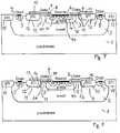
- the appended figure 7 shows a cross-section of a conventional high-voltage lateral diffused MOS device.
- the signs of the conductivity types (p and n conductivity) are inserted giving an example of an n-channel transistor.
- the conductivities are inverted in the case of a p-channel transistor.
- the present invention concerns either type of transistor.
- the signs of the conductivity are therefore only exemplary and do not restrict the scope of the invention.
- a substrate 1 of semiconductor material which may have a basic doping or may be intrinsically doped, is provided with a first well 2, in this example of n-type conductivity, and a second well 3 of the opposite conductivity type.
- the second well 3 is located within the first well 2, and both wells are disposed at an upper main surface of the substrate 1.
- the second well 3 is provided with a source region 4 having the conductivity type of the first well 2.
- the source region is preferably highly doped.
- the arrangement of the components of this device is preferably symmetrical around a vertical axis; and the two areas of the cross-section of the source region 4 in figure 7 show two portions of a single source region.
- a drain region 5 having the same type of conductivity as the source region 4 is arranged at the surface of the first well 2, surrounding the source region 4 and disposed concentrically with respect to the source region 4.
- the upper areas of the source and drain regions 4, 5 can be elliptic or similarly elongated in one direction.
- the geometrical shape is assumed to be a stripe in the following description.
- the space between the source region 4 and the drain region 5 is interrupted by an isolation region 12 formed by a shallow trench isolation, which forms an electrically insulating region. Between the source region 4 and the isolation region 12, the upper surface of the second well 3 forms the channel region 10 of the transistor. It is controlled by a gate electrode 8, which is arranged above the channel region 10 and electrically insulated from the semiconductor material by a thin gate dielectric 9. Between the channel region 10 and the drain region 5, the first well 2 provides a drift region 11 for the charge carriers moving from source to drain during the operation of the device. Preferably, a field plate 13 is disposed above the isolation region 12 and electrically connected to the gate electrode 8. A source contact 6 is applied to the source region 4.
- the source contact 6 is preferably also connected to the second well 3 via a highly doped contact region 14 of the same conductivity type as the second well 3.
- the drain region 5 is supplied with a drain contact 7.
- an optional outer isolation region 15 can be introduced in the device, which is preferably also formed by a shallow trench isolation.
- Figure 8 shows an improved embodiment of the device according to figure 7, which additionally comprises an edge region 26 under the inner edge of the isolation region 12.
- This conventional edge region 26 covers the edge 16 of the isolation region 12 and has the same conductivity type as the first well 2, but is doped with a higher concentration of the doping atoms.
- This embodiment aims at improving the on-state performance of the transistor by the introduction of extra n-type dopant at the STI edge in the drift region 11.
- This favorable approach may give rise to the generation of an extremely large number of hot carriers by further focusing the electric field to the STI edge. Therefore the difficulty of avoiding the electric field near the STI edge while at the same time maintaining the desired blocking voltage cannot be removed by this modification of the device, which is nevertheless an improvement in other respects.
- the lateral diffused MOS device is provided with an additional implanted edge region at the inner edge of the isolation region facing the drift region and the source region.
- the edge region has a conductivity type opposite to the conductivity type of the first well. In this way, the occurrence of a strong electric field at the edge of the isolation region and an acceleration of charge carriers up to an injection of hot carriers into the insulating material are avoided.
- the edge region is preferably produced by a further implantation step through a small mask opening in a layer of a material which fills the shallow trench and is selectively etchable with respect to the semiconductor material.
- a further edge region can be provided under the first edge region on the side opposite to the shallow trench isolation, in order to improve the drifting path of the charge carriers moving from source to drain through the drift region.
- the further edge region is provided with a conductivity type that is the same as the conductivity type of the first well and the drift region. An unfavorable partial bar of the drift region caused by the first edge region is thus compensated.
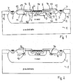
- FIG. 1 shows a cross-section of an embodiment of the LDMOS device.
- the principal structure is similar to the one already explained in connection with FIG. 7 and 8.
- Like reference numerals designate the corresponding device components, which are listed once more for the sake of completeness.
- the substrate 1 of semiconductor material is provided with a first well 2, a second well 3 disposed within the first well, a source region 4, a drain region 5, a source contact 6, a drain contact 7, a gate electrode 8, a gate dielectric 9, a channel region 10 located in the second well 3, a drift region 11 located between the channel region 10 and the drain region 5, and an isolation region 12 formed by a shallow trench isolation, preferably furthermore a field plate 13, a contact region 14 provided for the second well 3, and an outer isolation region 15.
- the edge region 17 is arranged under an inner edge 16 of the isolation region 12.
- the lateral and vertical extensions of the edge region 17 can be adapted to optimize the performance of the device.
- the edge region 17 is arranged in the vicinity of the edge 16 of the isolation region 12 and preferably covers the edge 16.
- the edge region 17 is preferably arranged to be contiguous with to the edge 16 and in contact with the insulating material. Thus, the volume occupied by the edge region 17 is excluded from the drift region 11. Since the drifting path of the charge carriers moving from source to drain is partially barred by the edge region 17, a further edge region can be provided as a compensation.
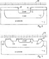
- FIG. 2 shows a second embodiment that is provided with a further edge region 18 to compensate for the effect of the first edge region 17.
- the first edge region 17 is provided with a conductivity type that is opposite to the conductivity of the first well 2 and the drift region 11
- the further edge region 18 is provided with the conductivity type of the drift region.
- the further edge region 18 is preferably doped with a higher concentration of doping atoms than the basic doping of the first well 2.
- the other components of the embodiment according to FIG. 2 correspond to the components of the embodiment of FIG. 1 and need not be specified any further.
- FIG. 3 shows a cross-section of an intermediate product comprising a substrate 1, a first well 2 and a second well 3 for the method step of the implantation 20 of the second well 3, indicated by arrows.
- the implantation is performed by means of a first mask 19, which covers the area surrounding the region provided for the second well 3.
- the substrate 1 is provided with a basic p-doping. Instead, it may be intrinsically doped, or the sign of the conductivities may be interchanged.
- FIG. 4 shows a further intermediate product for the step of the etching 22 of the shallow trenches 23 by means of a second mask 21.
- the shallow trenches 23 are preferably formed to a minor depth as compared to the n-well, which is indicated in an exemplary manner in FIG. 4.
- the depth of the inner shallow trench 23 can be varied according to the embodiment that has to be produced, the inner shallow trench 23 does not intercept the first well vertically. This allows the arrangement of source and drain on opposite sides of the inner shallow trench.
- the drift region is provided under the inner shallow trench.
- the outer shallow trench is optional and provided as an isolation from the adjacent device.
- FIG. 5 shows a further intermediate product in a cross-section according to FIG. 4.
- a third mask 24 is formed by the formation of openings in the material in the areas where the edge regions are to be arranged.
- a further implantation 25 is performed to implant the dopant provided for the edge region 17, as well as, preferably, a second dopant provided for the opposite type of conductivity and provided for the further edge region 18, implanted slightly deeper than the dopant provided for the first edge region 17.
- the signs of conductivity are indicated in FIG. 5 for the example of an n-channel transistor. As has already been mentioned, the conductivity types can be interchanged.
- the openings in the third mask 24 are then filled, preferably with the same material that has already been applied to fill the shallow trenches.
- the material of the third mask 24 can be completely removed and substituted with a dielectric material that is provided for the formation of shallow trench isolations.
- the material that is first applied to fill the trenches is selected to be selectively etchable with respect to the semiconductor material so that the openings can be formed without attacking the semiconductor material, in order to avoid a deterioration of the drift region. It is also possible to leave a thin layer of the material of the third mask 24 on the semiconductor surface, thus slightly screening the subsequent implantation 25.
- FIG. 6 shows the intermediate product according to FIG. 5 for a variant of the production method.
- the openings in the third mask 24 are formed broader in order to uncover marginal areas of the upper substrate surface adjacent to the shallow trench.
- the edge region 17 and, if provided, the further edge region 18 are formed to cover the whole edge of the isolation region 12.
- edge region 17 Since the edge region 17 is surrounded by dielectric material and semiconductor material of opposite type of conductivity, the edge region 17 is kept floating, without being directly connected to any of the applied voltages.
- the device performance on-state is improved by the modification of the drift region by the further edge region 18.
- the described structures of the preferred embodiments of n-channel transistors are, except for the signs of conductivity, equivalent to the structures of p-channel LDMOS transistors according to this invention.
- the peak of the electric field is shifted from the edge of the STI at the side facing the gate to the drain side of the STI.
- the generation of hot carriers is suppressed or at least essentially reduced at the edge of the STI facing the gate without degrading the on-state current handling capability of the transistor.
- This is a significant improvement of the LDMOS device, especially as the blocking voltages of the conventional device is essentially maintained.
Landscapes
- Insulated Gate Type Field-Effect Transistor (AREA)
- Bipolar Transistors (AREA)
Abstract

Description
- This invention concerns a lateral diffused MOS transistor for high-voltage applications and a method of producing such a device.
- High-voltage LDMOS (lateral double-diffused MOS) transistors are widely used for output devices in smart power applications. For a scaling-down of the process technology below dimensions of 0.25 µm, shallow trench isolations (STI) have to be introduced in the HV-LDMOS transistors. However, STI causes reliability problems, especially problems arising from the generation of large numbers of hot carriers and stress related leakage currents in the vicinity of the edges of the STI regions. During high-voltage operations, a strong electric field occurs at the edges of the shallow trench isolation. Due to the focusing of the electric field, electrons and holes generated by impact ionization can be sufficiently accelerated to gain enough kinetic energy to be injected into the dielectric material, which is typically oxide. The electrons and holes having a large kinetic energy, called hot carriers, interact with the dielectric material and can generate defects, especially at the interface between the semiconductor material and the insulator, typically silicon and silicon dioxide, and in the silicon dioxide, thus causing a shift in the electric characteristics of the performance of the semiconductor device. Therefore, the generation of large numbers of hot carriers in the vicinity of the shallow trench isolations is detrimental to the long-term reliability of the device, and these undesirable effects are preferably avoided.
- Furthermore, carriers that are generated mainly at the STI edges are injected from the drift region into the body region and cause a turn-on of the parasitic bipolar transistor formed by the sequence of doped layers having alternating types of conductivity. A strong electric field in the vicinity of the STI edges has therefore to be avoided as much as possible in order to prevent a device degradation due to the induced hot carriers and to improve the electrical safe operation area (SOA).
- The appended figure 7 shows a cross-section of a conventional high-voltage lateral diffused MOS device. The signs of the conductivity types (p and n conductivity) are inserted giving an example of an n-channel transistor. The conductivities are inverted in the case of a p-channel transistor. The present invention concerns either type of transistor. The signs of the conductivity are therefore only exemplary and do not restrict the scope of the invention. A
substrate 1 of semiconductor material, which may have a basic doping or may be intrinsically doped, is provided with afirst well 2, in this example of n-type conductivity, and a second well 3 of the opposite conductivity type. The second well 3 is located within thefirst well 2, and both wells are disposed at an upper main surface of thesubstrate 1. The second well 3 is provided with asource region 4 having the conductivity type of thefirst well 2. The source region is preferably highly doped. The arrangement of the components of this device is preferably symmetrical around a vertical axis; and the two areas of the cross-section of thesource region 4 in figure 7 show two portions of a single source region. Adrain region 5 having the same type of conductivity as thesource region 4 is arranged at the surface of thefirst well 2, surrounding thesource region 4 and disposed concentrically with respect to thesource region 4. Instead of a circular arrangement, the upper areas of the source anddrain regions - The space between the
source region 4 and thedrain region 5 is interrupted by anisolation region 12 formed by a shallow trench isolation, which forms an electrically insulating region. Between thesource region 4 and theisolation region 12, the upper surface of the second well 3 forms thechannel region 10 of the transistor. It is controlled by agate electrode 8, which is arranged above thechannel region 10 and electrically insulated from the semiconductor material by a thin gate dielectric 9. Between thechannel region 10 and thedrain region 5, thefirst well 2 provides adrift region 11 for the charge carriers moving from source to drain during the operation of the device. Preferably, afield plate 13 is disposed above theisolation region 12 and electrically connected to thegate electrode 8. A source contact 6 is applied to thesource region 4. The source contact 6 is preferably also connected to the second well 3 via a highlydoped contact region 14 of the same conductivity type as the second well 3. Thedrain region 5 is supplied with a drain contact 7. For better isolation between adjacent devices, an optionalouter isolation region 15 can be introduced in the device, which is preferably also formed by a shallow trench isolation. - Figure 8 shows an improved embodiment of the device according to figure 7, which additionally comprises an
edge region 26 under the inner edge of theisolation region 12. Thisconventional edge region 26 covers theedge 16 of theisolation region 12 and has the same conductivity type as thefirst well 2, but is doped with a higher concentration of the doping atoms. This embodiment aims at improving the on-state performance of the transistor by the introduction of extra n-type dopant at the STI edge in thedrift region 11. However, especially this favorable approach may give rise to the generation of an extremely large number of hot carriers by further focusing the electric field to the STI edge. Therefore the difficulty of avoiding the electric field near the STI edge while at the same time maintaining the desired blocking voltage cannot be removed by this modification of the device, which is nevertheless an improvement in other respects. - It is an object of this invention to present an improved lateral diffused MOS device that avoids the aforementioned problems. It is a further object to disclose a method for producing such an improved device.
- This object and further objects are achieved by the lateral diffused MOS device having the features according to the limitations of
claim 1 and by the method having the method steps according to the limitations of claim 7, respectively. Further embodiments, alterations or substitutions emerge from the dependent claims. - The lateral diffused MOS device is provided with an additional implanted edge region at the inner edge of the isolation region facing the drift region and the source region. The edge region has a conductivity type opposite to the conductivity type of the first well. In this way, the occurrence of a strong electric field at the edge of the isolation region and an acceleration of charge carriers up to an injection of hot carriers into the insulating material are avoided.
- The edge region is preferably produced by a further implantation step through a small mask opening in a layer of a material which fills the shallow trench and is selectively etchable with respect to the semiconductor material. A further edge region can be provided under the first edge region on the side opposite to the shallow trench isolation, in order to improve the drifting path of the charge carriers moving from source to drain through the drift region. The further edge region is provided with a conductivity type that is the same as the conductivity type of the first well and the drift region. An unfavorable partial bar of the drift region caused by the first edge region is thus compensated.
- A more detailed description of examples of the invention will now be given in connection with the appended figures.
- FIG. 1 shows a cross-section of a first embodiment of the LDMOS.
- FIG. 2 shows a cross-section of a second embodiment of the LDMOS.
- FIG. 3 shows a cross-section of a first intermediate product of a preferred production method.
- FIG. 4 shows a cross-section according to FIG. 3 of a further intermediate product after the formation of shallow trenches.
- FIG. 5 shows a cross-section according to FIG. 4 of a further intermediate product after the formation of an edge region.
- FIG. 6 shows a cross-section according to FIG. 5 for an alternative embodiment.
- FIG. 7 shows a cross-section of a conventional LDMOS device.
- FIG. 8 shows a cross-section of an improved conventional LDMOS device.
- FIG. 1 shows a cross-section of an embodiment of the LDMOS device. The principal structure is similar to the one already explained in connection with FIG. 7 and 8. Like reference numerals designate the corresponding device components, which are listed once more for the sake of completeness. The
substrate 1 of semiconductor material is provided with afirst well 2, a second well 3 disposed within the first well, asource region 4, adrain region 5, a source contact 6, a drain contact 7, agate electrode 8, a gate dielectric 9, achannel region 10 located in the second well 3, adrift region 11 located between thechannel region 10 and thedrain region 5, and anisolation region 12 formed by a shallow trench isolation, preferably furthermore afield plate 13, acontact region 14 provided for the second well 3, and anouter isolation region 15. Theedge region 17 is arranged under aninner edge 16 of theisolation region 12. The lateral and vertical extensions of theedge region 17 can be adapted to optimize the performance of the device. Theedge region 17 is arranged in the vicinity of theedge 16 of theisolation region 12 and preferably covers theedge 16. Theedge region 17 is preferably arranged to be contiguous with to theedge 16 and in contact with the insulating material. Thus, the volume occupied by theedge region 17 is excluded from thedrift region 11. Since the drifting path of the charge carriers moving from source to drain is partially barred by theedge region 17, a further edge region can be provided as a compensation. - FIG. 2 shows a second embodiment that is provided with a
further edge region 18 to compensate for the effect of thefirst edge region 17. Whereas thefirst edge region 17 is provided with a conductivity type that is opposite to the conductivity of thefirst well 2 and thedrift region 11, thefurther edge region 18 is provided with the conductivity type of the drift region. Thefurther edge region 18 is preferably doped with a higher concentration of doping atoms than the basic doping of thefirst well 2. The other components of the embodiment according to FIG. 2 correspond to the components of the embodiment of FIG. 1 and need not be specified any further. - Further preferred embodiments will emerge from the description of a preferred method of production of this device in conjunction with FIGs. 3 to 6. FIG. 3 shows a cross-section of an intermediate product comprising a
substrate 1, afirst well 2 and a second well 3 for the method step of theimplantation 20 of the second well 3, indicated by arrows. The implantation is performed by means of afirst mask 19, which covers the area surrounding the region provided for the second well 3. In this example, thesubstrate 1 is provided with a basic p-doping. Instead, it may be intrinsically doped, or the sign of the conductivities may be interchanged. - FIG. 4 shows a further intermediate product for the step of the
etching 22 of theshallow trenches 23 by means of asecond mask 21. Theshallow trenches 23 are preferably formed to a minor depth as compared to the n-well, which is indicated in an exemplary manner in FIG. 4. Although the depth of the innershallow trench 23 can be varied according to the embodiment that has to be produced, the innershallow trench 23 does not intercept the first well vertically. This allows the arrangement of source and drain on opposite sides of the inner shallow trench. The drift region is provided under the inner shallow trench. The outer shallow trench is optional and provided as an isolation from the adjacent device. - FIG. 5 shows a further intermediate product in a cross-section according to FIG. 4. After the
shallow trenches 23 have been filled with a material that is selectively etchable with respect to the semiconductor material, athird mask 24 is formed by the formation of openings in the material in the areas where the edge regions are to be arranged. Then afurther implantation 25 is performed to implant the dopant provided for theedge region 17, as well as, preferably, a second dopant provided for the opposite type of conductivity and provided for thefurther edge region 18, implanted slightly deeper than the dopant provided for thefirst edge region 17. The signs of conductivity are indicated in FIG. 5 for the example of an n-channel transistor. As has already been mentioned, the conductivity types can be interchanged. The openings in thethird mask 24 are then filled, preferably with the same material that has already been applied to fill the shallow trenches. Alternatively, the material of thethird mask 24 can be completely removed and substituted with a dielectric material that is provided for the formation of shallow trench isolations. In any case, the material that is first applied to fill the trenches is selected to be selectively etchable with respect to the semiconductor material so that the openings can be formed without attacking the semiconductor material, in order to avoid a deterioration of the drift region. It is also possible to leave a thin layer of the material of thethird mask 24 on the semiconductor surface, thus slightly screening thesubsequent implantation 25. - FIG. 6 shows the intermediate product according to FIG. 5 for a variant of the production method. In this embodiment, the openings in the
third mask 24 are formed broader in order to uncover marginal areas of the upper substrate surface adjacent to the shallow trench. In this manner, theedge region 17 and, if provided, thefurther edge region 18 are formed to cover the whole edge of theisolation region 12. - Since the
edge region 17 is surrounded by dielectric material and semiconductor material of opposite type of conductivity, theedge region 17 is kept floating, without being directly connected to any of the applied voltages. The device performance on-state is improved by the modification of the drift region by thefurther edge region 18. The described structures of the preferred embodiments of n-channel transistors are, except for the signs of conductivity, equivalent to the structures of p-channel LDMOS transistors according to this invention. By the introduction of the floating region at the edge of the STI, the electric field at the STI edge can effectively be reduced. An extra doping of the conductivity type of thesecond well 2 compensates for an increase of on-resistance due to the floating edge region. With the inventive structure, the peak of the electric field is shifted from the edge of the STI at the side facing the gate to the drain side of the STI. Thus, the generation of hot carriers is suppressed or at least essentially reduced at the edge of the STI facing the gate without degrading the on-state current handling capability of the transistor. This is a significant improvement of the LDMOS device, especially as the blocking voltages of the conventional device is essentially maintained. - List of reference numerals
- 1
- substrate
- 2
- first well
- 3
- second well
- 4
- source region
- 5
- drain region
- 6
- source contact
- 7
- drain contact
- 8
- gate electrode
- 9
- gate dielectric
- 10
- channel region
- 11
- drift region
- 12
- isolation region (STI, shallow trench isolation)
- 13
- field plate
- 14
- contact region
- 15
- outer isolation region
- 16
- edge of the isolation region
- 17
- edge region
- 18
- further edge region
- 19
- first mask
- 20
- implantation
- 21
- second mask
- 22
- etching
- 23
- shallow trench
- 24
- third mask
- 25
- further implantation
- 26
- conventional diffused edge region
Claims (10)
- Lateral diffused MOS device comprising
a semiconductor substrate (1) with a main surface,
a first well (2) of a first conductivity type at the main surface,
a second well (3) of an opposite second conductivity type at the main surface within the first well (2),
a diffused source region (4) of the first conductivity type in the second well (3),
a diffused drain region (5) of the first conductivity type in the first well (2),
a channel region (10) provided at the main surface in the second well (3) between the source region (4) and the drain region (5),
a drift region (11) provided in the first well (2) between the channel region (10) and the drain region (5),
a gate electrode (8) arranged above the channel region (10) and insulated from the channel region (10) by a gate dielectric (9),
a shallow isolation region (12) arranged at the main surface above the drift region (11), said isolation region (12) having an edge (16) facing the drift region (11) and the source region (4), and
an edge region (17) of the second conductivity type arranged at said edge (16) of the isolation region (12). - Lateral diffused MOS device according to claim 1, further comprising
a further edge region (18) of the first conductivity type arranged in the drift region (11) at said edge region (17). - Lateral diffused MOS device according to claim 2, wherein said further edge region (18) is disposed contiguous to said edge region (17) on the side facing away from the isolation region (12).
- Lateral diffused MOS device according to one of claims 1 to 3, wherein
the isolation region (12) is in the form of a shallow trench isolation. - Lateral diffused MOS device according to one of claims 1 to 4, further comprising
a field plate (13) of electrically conductive material connected to the gate electrode (8) and located on the isolation region (12). - Lateral diffused MOS device according to one of claims 1 to 5, wherein
the isolation region (12) is spaced apart from the second well (3) and
the drift region (11) is partially located between the channel region (10) and the isolation region (12). - Method for production of a lateral diffused MOS device, comprising
providing a substrate (1) of semiconductor material at a main surface with a first well (2) of a first conductivity type and with a second well (3) of an opposite second conductivity type arranged within the first well (2),
etching a shallow trench (23) in a surface area of the first well (2),
filling the shallow trench (23) with a material that is selectively etchable with respect to the semiconductor material,
forming an opening in the material filling the shallow trench (23) above a bottom edge of the trench that faces the second well (3), and,
using the remaining material as a mask (24), performing an implantation (25) of a dopant provided for the second conductivity type. - Method according to claim 7, wherein
the shallow trench (23) is filled with a material that is suitable to form a shallow trench isolation. - Method according to claim 7 or 8, further comprising performing an implantation of a dopant provided for the first conductivity type slightly deeper than the implantation of the dopant provided for the second conductivity type.
- Method according to one of claims 7 to 9, further comprising
performing a subsequent further implantation to form regions of source and drain of the first conductivity type.
Priority Applications (3)
| Application Number | Priority Date | Filing Date | Title |
|---|---|---|---|
| AT06017058T ATE484075T1 (en) | 2006-08-16 | 2006-08-16 | METHOD FOR PRODUCING A LATERAL DMOS ARRANGEMENT |
| EP06017058A EP1890335B1 (en) | 2006-08-16 | 2006-08-16 | Method of making a lateral DMOS device |
| DE602006017364T DE602006017364D1 (en) | 2006-08-16 | 2006-08-16 | Method of making a lateral DMOS device |
Applications Claiming Priority (1)
| Application Number | Priority Date | Filing Date | Title |
|---|---|---|---|
| EP06017058A EP1890335B1 (en) | 2006-08-16 | 2006-08-16 | Method of making a lateral DMOS device |
Publications (2)
| Publication Number | Publication Date |
|---|---|
| EP1890335A1 true EP1890335A1 (en) | 2008-02-20 |
| EP1890335B1 EP1890335B1 (en) | 2010-10-06 |
Family
ID=37564192
Family Applications (1)
| Application Number | Title | Priority Date | Filing Date |
|---|---|---|---|
| EP06017058A Not-in-force EP1890335B1 (en) | 2006-08-16 | 2006-08-16 | Method of making a lateral DMOS device |
Country Status (3)
| Country | Link |
|---|---|
| EP (1) | EP1890335B1 (en) |
| AT (1) | ATE484075T1 (en) |
| DE (1) | DE602006017364D1 (en) |
Cited By (5)
| Publication number | Priority date | Publication date | Assignee | Title |
|---|---|---|---|---|
| CN103077895A (en) * | 2012-12-19 | 2013-05-01 | 上海宏力半导体制造有限公司 | Laterally diffused metal oxide semiconductor (LDMOS) transistor and formation method thereof |
| EP2392028B1 (en) * | 2009-01-30 | 2018-08-22 | Altera Corporation | Integrated circuit with doped substrate and with an inductor |
| CN114068701A (en) * | 2020-07-30 | 2022-02-18 | 中芯北方集成电路制造(北京)有限公司 | Semiconductor structure and forming method thereof |
| US20220384247A1 (en) * | 2021-05-28 | 2022-12-01 | Taiwan Semiconductor Manufacturing Company Ltd. | Semiconductor device and method of manufacturing the same |
| CN115939141A (en) * | 2023-01-19 | 2023-04-07 | 北京智芯微电子科技有限公司 | Fully isolated lateral double diffused semiconductor device and method of manufacture |
Citations (2)
| Publication number | Priority date | Publication date | Assignee | Title |
|---|---|---|---|---|
| US20030001216A1 (en) | 2001-06-27 | 2003-01-02 | Motorola, Inc. | Semiconductor component and method of manufacturing |
| US20050112822A1 (en) | 2003-11-21 | 2005-05-26 | Andrej Litwin | Method in the fabrication of a monolithically integrated high frequency circuit |
-
2006
- 2006-08-16 EP EP06017058A patent/EP1890335B1/en not_active Not-in-force
- 2006-08-16 DE DE602006017364T patent/DE602006017364D1/en active Active
- 2006-08-16 AT AT06017058T patent/ATE484075T1/en not_active IP Right Cessation
Patent Citations (2)
| Publication number | Priority date | Publication date | Assignee | Title |
|---|---|---|---|---|
| US20030001216A1 (en) | 2001-06-27 | 2003-01-02 | Motorola, Inc. | Semiconductor component and method of manufacturing |
| US20050112822A1 (en) | 2003-11-21 | 2005-05-26 | Andrej Litwin | Method in the fabrication of a monolithically integrated high frequency circuit |
Cited By (7)
| Publication number | Priority date | Publication date | Assignee | Title |
|---|---|---|---|---|
| EP2392028B1 (en) * | 2009-01-30 | 2018-08-22 | Altera Corporation | Integrated circuit with doped substrate and with an inductor |
| CN103077895A (en) * | 2012-12-19 | 2013-05-01 | 上海宏力半导体制造有限公司 | Laterally diffused metal oxide semiconductor (LDMOS) transistor and formation method thereof |
| CN114068701A (en) * | 2020-07-30 | 2022-02-18 | 中芯北方集成电路制造(北京)有限公司 | Semiconductor structure and forming method thereof |
| CN114068701B (en) * | 2020-07-30 | 2024-03-19 | 中芯北方集成电路制造(北京)有限公司 | Semiconductor structure and forming method thereof |
| US20220384247A1 (en) * | 2021-05-28 | 2022-12-01 | Taiwan Semiconductor Manufacturing Company Ltd. | Semiconductor device and method of manufacturing the same |
| US11676850B2 (en) * | 2021-05-28 | 2023-06-13 | Taiwan Semiconductor Manufacturing Company Ltd. | Semiconductor device and method of manufacturing the same |
| CN115939141A (en) * | 2023-01-19 | 2023-04-07 | 北京智芯微电子科技有限公司 | Fully isolated lateral double diffused semiconductor device and method of manufacture |
Also Published As
| Publication number | Publication date |
|---|---|
| EP1890335B1 (en) | 2010-10-06 |
| DE602006017364D1 (en) | 2010-11-18 |
| ATE484075T1 (en) | 2010-10-15 |
Similar Documents
| Publication | Publication Date | Title |
|---|---|---|
| US8304329B2 (en) | Power device structures and methods | |
| CN100585875C (en) | LDMOS transistor | |
| US8294235B2 (en) | Edge termination with improved breakdown voltage | |
| US7687851B2 (en) | High density trench MOSFET with reduced on-resistance | |
| CN106887452B (en) | Self-Adjustable Isolation Biasing in Semiconductor Devices | |
| US7928508B2 (en) | Disconnected DPW structures for improving on-state performance of MOS devices | |
| EP2338177B1 (en) | Insulated gate semiconductor device and method of manufacturing the same | |
| KR20170026109A (en) | Semiconductor device and semiconductor device manufacturing method | |
| CN1602544A (en) | Method for making high voltage MOS transistor by ion implantation | |
| US7074681B2 (en) | Semiconductor component and method of manufacturing | |
| US11631763B2 (en) | Termination for trench field plate power MOSFET | |
| EP4228003A1 (en) | Semiconductor device having a current spreading region | |
| KR100825466B1 (en) | High-voltage NMOS-transistor and associated production method | |
| US9735244B2 (en) | Quasi-vertical structure having a sidewall implantation for high voltage MOS device and method of forming the same | |
| JP4232645B2 (en) | Trench lateral semiconductor device and manufacturing method thereof | |
| EP1890335B1 (en) | Method of making a lateral DMOS device | |
| US20250185320A1 (en) | Semiconductor component and method for producing a semiconductor component | |
| US20240234495A1 (en) | Gate trench power semiconductor devices having self-aligned trench shielding regions and related methods | |
| JP4150704B2 (en) | Horizontal short channel DMOS | |
| US20250311361A1 (en) | Semiconductor device | |
| US12396250B2 (en) | Vertical IGBT with complementary channel for hole extraction | |
| EP4394889A1 (en) | Semiconductor device and method for producing a semiconductor device | |
| WO2013163462A2 (en) | Compact tid hardening nmos device and fabrication process | |
| JP2024074426A (en) | Semiconductor device and its manufacturing method | |
| JP2026068823A (en) | Silicon carbide semiconductor device and method for manufacturing a silicon carbide semiconductor device |
Legal Events
| Date | Code | Title | Description |
|---|---|---|---|
| PUAI | Public reference made under article 153(3) epc to a published international application that has entered the european phase |
Free format text: ORIGINAL CODE: 0009012 |
|
| AK | Designated contracting states |
Kind code of ref document: A1 Designated state(s): AT BE BG CH CY CZ DE DK EE ES FI FR GB GR HU IE IS IT LI LT LU LV MC NL PL PT RO SE SI SK TR |
|
| AX | Request for extension of the european patent |
Extension state: AL BA HR MK YU |
|
| 17P | Request for examination filed |
Effective date: 20080818 |
|
| 17Q | First examination report despatched |
Effective date: 20080919 |
|
| AKX | Designation fees paid |
Designated state(s): AT BE BG CH CY CZ DE DK EE ES FI FR GB GR HU IE IS IT LI LT LU LV MC NL PL PT RO SE SI SK TR |
|
| RTI1 | Title (correction) |
Free format text: METHOD OF MAKING A LATERAL DMOS DEVICE |
|
| GRAP | Despatch of communication of intention to grant a patent |
Free format text: ORIGINAL CODE: EPIDOSNIGR1 |
|
| GRAS | Grant fee paid |
Free format text: ORIGINAL CODE: EPIDOSNIGR3 |
|
| GRAA | (expected) grant |
Free format text: ORIGINAL CODE: 0009210 |
|
| AK | Designated contracting states |
Kind code of ref document: B1 Designated state(s): AT BE BG CH CY CZ DE DK EE ES FI FR GB GR HU IE IS IT LI LT LU LV MC NL PL PT RO SE SI SK TR |
|
| REG | Reference to a national code |
Ref country code: GB Ref legal event code: FG4D |
|
| REG | Reference to a national code |
Ref country code: CH Ref legal event code: EP |
|
| REG | Reference to a national code |
Ref country code: IE Ref legal event code: FG4D |
|
| REF | Corresponds to: |
Ref document number: 602006017364 Country of ref document: DE Date of ref document: 20101118 Kind code of ref document: P |
|
| REG | Reference to a national code |
Ref country code: NL Ref legal event code: VDEP Effective date: 20101006 |
|
| PG25 | Lapsed in a contracting state [announced via postgrant information from national office to epo] |
Ref country code: SI Free format text: LAPSE BECAUSE OF FAILURE TO SUBMIT A TRANSLATION OF THE DESCRIPTION OR TO PAY THE FEE WITHIN THE PRESCRIBED TIME-LIMIT Effective date: 20101006 |
|
| LTIE | Lt: invalidation of european patent or patent extension |
Effective date: 20101006 |
|
| PG25 | Lapsed in a contracting state [announced via postgrant information from national office to epo] |
Ref country code: LT Free format text: LAPSE BECAUSE OF FAILURE TO SUBMIT A TRANSLATION OF THE DESCRIPTION OR TO PAY THE FEE WITHIN THE PRESCRIBED TIME-LIMIT Effective date: 20101006 |
|
| PG25 | Lapsed in a contracting state [announced via postgrant information from national office to epo] |
Ref country code: LV Free format text: LAPSE BECAUSE OF FAILURE TO SUBMIT A TRANSLATION OF THE DESCRIPTION OR TO PAY THE FEE WITHIN THE PRESCRIBED TIME-LIMIT Effective date: 20101006 Ref country code: PT Free format text: LAPSE BECAUSE OF FAILURE TO SUBMIT A TRANSLATION OF THE DESCRIPTION OR TO PAY THE FEE WITHIN THE PRESCRIBED TIME-LIMIT Effective date: 20110207 Ref country code: BG Free format text: LAPSE BECAUSE OF FAILURE TO SUBMIT A TRANSLATION OF THE DESCRIPTION OR TO PAY THE FEE WITHIN THE PRESCRIBED TIME-LIMIT Effective date: 20110106 Ref country code: SE Free format text: LAPSE BECAUSE OF FAILURE TO SUBMIT A TRANSLATION OF THE DESCRIPTION OR TO PAY THE FEE WITHIN THE PRESCRIBED TIME-LIMIT Effective date: 20101006 Ref country code: NL Free format text: LAPSE BECAUSE OF FAILURE TO SUBMIT A TRANSLATION OF THE DESCRIPTION OR TO PAY THE FEE WITHIN THE PRESCRIBED TIME-LIMIT Effective date: 20101006 Ref country code: IS Free format text: LAPSE BECAUSE OF FAILURE TO SUBMIT A TRANSLATION OF THE DESCRIPTION OR TO PAY THE FEE WITHIN THE PRESCRIBED TIME-LIMIT Effective date: 20110206 Ref country code: FI Free format text: LAPSE BECAUSE OF FAILURE TO SUBMIT A TRANSLATION OF THE DESCRIPTION OR TO PAY THE FEE WITHIN THE PRESCRIBED TIME-LIMIT Effective date: 20101006 Ref country code: AT Free format text: LAPSE BECAUSE OF FAILURE TO SUBMIT A TRANSLATION OF THE DESCRIPTION OR TO PAY THE FEE WITHIN THE PRESCRIBED TIME-LIMIT Effective date: 20101006 |
|
| PG25 | Lapsed in a contracting state [announced via postgrant information from national office to epo] |
Ref country code: BE Free format text: LAPSE BECAUSE OF FAILURE TO SUBMIT A TRANSLATION OF THE DESCRIPTION OR TO PAY THE FEE WITHIN THE PRESCRIBED TIME-LIMIT Effective date: 20101006 Ref country code: GR Free format text: LAPSE BECAUSE OF FAILURE TO SUBMIT A TRANSLATION OF THE DESCRIPTION OR TO PAY THE FEE WITHIN THE PRESCRIBED TIME-LIMIT Effective date: 20110107 |
|
| PG25 | Lapsed in a contracting state [announced via postgrant information from national office to epo] |
Ref country code: ES Free format text: LAPSE BECAUSE OF FAILURE TO SUBMIT A TRANSLATION OF THE DESCRIPTION OR TO PAY THE FEE WITHIN THE PRESCRIBED TIME-LIMIT Effective date: 20110117 Ref country code: EE Free format text: LAPSE BECAUSE OF FAILURE TO SUBMIT A TRANSLATION OF THE DESCRIPTION OR TO PAY THE FEE WITHIN THE PRESCRIBED TIME-LIMIT Effective date: 20101006 Ref country code: CZ Free format text: LAPSE BECAUSE OF FAILURE TO SUBMIT A TRANSLATION OF THE DESCRIPTION OR TO PAY THE FEE WITHIN THE PRESCRIBED TIME-LIMIT Effective date: 20101006 |
|
| PLBE | No opposition filed within time limit |
Free format text: ORIGINAL CODE: 0009261 |
|
| STAA | Information on the status of an ep patent application or granted ep patent |
Free format text: STATUS: NO OPPOSITION FILED WITHIN TIME LIMIT |
|
| PG25 | Lapsed in a contracting state [announced via postgrant information from national office to epo] |
Ref country code: SK Free format text: LAPSE BECAUSE OF FAILURE TO SUBMIT A TRANSLATION OF THE DESCRIPTION OR TO PAY THE FEE WITHIN THE PRESCRIBED TIME-LIMIT Effective date: 20101006 Ref country code: RO Free format text: LAPSE BECAUSE OF FAILURE TO SUBMIT A TRANSLATION OF THE DESCRIPTION OR TO PAY THE FEE WITHIN THE PRESCRIBED TIME-LIMIT Effective date: 20101006 Ref country code: PL Free format text: LAPSE BECAUSE OF FAILURE TO SUBMIT A TRANSLATION OF THE DESCRIPTION OR TO PAY THE FEE WITHIN THE PRESCRIBED TIME-LIMIT Effective date: 20101006 Ref country code: DK Free format text: LAPSE BECAUSE OF FAILURE TO SUBMIT A TRANSLATION OF THE DESCRIPTION OR TO PAY THE FEE WITHIN THE PRESCRIBED TIME-LIMIT Effective date: 20101006 |
|
| 26N | No opposition filed |
Effective date: 20110707 |
|
| REG | Reference to a national code |
Ref country code: DE Ref legal event code: R097 Ref document number: 602006017364 Country of ref document: DE Effective date: 20110707 |
|
| PG25 | Lapsed in a contracting state [announced via postgrant information from national office to epo] |
Ref country code: IT Free format text: LAPSE BECAUSE OF FAILURE TO SUBMIT A TRANSLATION OF THE DESCRIPTION OR TO PAY THE FEE WITHIN THE PRESCRIBED TIME-LIMIT Effective date: 20101006 |
|
| PG25 | Lapsed in a contracting state [announced via postgrant information from national office to epo] |
Ref country code: MC Free format text: LAPSE BECAUSE OF NON-PAYMENT OF DUE FEES Effective date: 20110831 |
|
| REG | Reference to a national code |
Ref country code: CH Ref legal event code: PL |
|
| GBPC | Gb: european patent ceased through non-payment of renewal fee |
Effective date: 20110816 |
|
| PG25 | Lapsed in a contracting state [announced via postgrant information from national office to epo] |
Ref country code: CH Free format text: LAPSE BECAUSE OF NON-PAYMENT OF DUE FEES Effective date: 20110831 Ref country code: LI Free format text: LAPSE BECAUSE OF NON-PAYMENT OF DUE FEES Effective date: 20110831 |
|
| REG | Reference to a national code |
Ref country code: FR Ref legal event code: ST Effective date: 20120430 |
|
| REG | Reference to a national code |
Ref country code: IE Ref legal event code: MM4A |
|
| PG25 | Lapsed in a contracting state [announced via postgrant information from national office to epo] |
Ref country code: IE Free format text: LAPSE BECAUSE OF NON-PAYMENT OF DUE FEES Effective date: 20110816 |
|
| PG25 | Lapsed in a contracting state [announced via postgrant information from national office to epo] |
Ref country code: FR Free format text: LAPSE BECAUSE OF NON-PAYMENT OF DUE FEES Effective date: 20110831 Ref country code: GB Free format text: LAPSE BECAUSE OF NON-PAYMENT OF DUE FEES Effective date: 20110816 |
|
| PG25 | Lapsed in a contracting state [announced via postgrant information from national office to epo] |
Ref country code: LU Free format text: LAPSE BECAUSE OF NON-PAYMENT OF DUE FEES Effective date: 20110816 Ref country code: CY Free format text: LAPSE BECAUSE OF EXPIRATION OF PROTECTION Effective date: 20101006 |
|
| PG25 | Lapsed in a contracting state [announced via postgrant information from national office to epo] |
Ref country code: TR Free format text: LAPSE BECAUSE OF FAILURE TO SUBMIT A TRANSLATION OF THE DESCRIPTION OR TO PAY THE FEE WITHIN THE PRESCRIBED TIME-LIMIT Effective date: 20101006 |
|
| PG25 | Lapsed in a contracting state [announced via postgrant information from national office to epo] |
Ref country code: HU Free format text: LAPSE BECAUSE OF FAILURE TO SUBMIT A TRANSLATION OF THE DESCRIPTION OR TO PAY THE FEE WITHIN THE PRESCRIBED TIME-LIMIT Effective date: 20101006 |
|
| PGFP | Annual fee paid to national office [announced via postgrant information from national office to epo] |
Ref country code: DE Payment date: 20220819 Year of fee payment: 17 |
|
| P01 | Opt-out of the competence of the unified patent court (upc) registered |
Effective date: 20230822 |
|
| REG | Reference to a national code |
Ref country code: DE Ref legal event code: R119 Ref document number: 602006017364 Country of ref document: DE |
|
| PG25 | Lapsed in a contracting state [announced via postgrant information from national office to epo] |
Ref country code: DE Free format text: LAPSE BECAUSE OF NON-PAYMENT OF DUE FEES Effective date: 20240301 |