EP1890305A1 - Condensateur variable MEMS et son procédé de fabrication - Google Patents
Condensateur variable MEMS et son procédé de fabrication Download PDFInfo
- Publication number
- EP1890305A1 EP1890305A1 EP07102351A EP07102351A EP1890305A1 EP 1890305 A1 EP1890305 A1 EP 1890305A1 EP 07102351 A EP07102351 A EP 07102351A EP 07102351 A EP07102351 A EP 07102351A EP 1890305 A1 EP1890305 A1 EP 1890305A1
- Authority
- EP
- European Patent Office
- Prior art keywords
- variable capacitor
- electrodes
- capacitor according
- support structure
- actuation
- Prior art date
- Legal status (The legal status is an assumption and is not a legal conclusion. Google has not performed a legal analysis and makes no representation as to the accuracy of the status listed.)
- Withdrawn
Links
- 239000003990 capacitor Substances 0.000 title claims abstract description 80
- 238000004519 manufacturing process Methods 0.000 title claims description 8
- 238000000034 method Methods 0.000 claims abstract description 25
- 230000008569 process Effects 0.000 claims abstract description 17
- 239000000758 substrate Substances 0.000 claims description 37
- 239000002184 metal Substances 0.000 claims description 8
- 238000000059 patterning Methods 0.000 claims description 6
- 238000012800 visualization Methods 0.000 description 8
- 239000011521 glass Substances 0.000 description 7
- 229920002120 photoresistant polymer Polymers 0.000 description 7
- UMIVXZPTRXBADB-UHFFFAOYSA-N benzocyclobutene Chemical compound C1=CC=C2CCC2=C1 UMIVXZPTRXBADB-UHFFFAOYSA-N 0.000 description 6
- 238000013461 design Methods 0.000 description 6
- 238000009826 distribution Methods 0.000 description 6
- 230000007246 mechanism Effects 0.000 description 6
- 238000012545 processing Methods 0.000 description 6
- 238000005516 engineering process Methods 0.000 description 5
- 230000005684 electric field Effects 0.000 description 4
- 238000001000 micrograph Methods 0.000 description 4
- 230000000737 periodic effect Effects 0.000 description 4
- 239000004642 Polyimide Substances 0.000 description 3
- 230000008901 benefit Effects 0.000 description 3
- 230000005540 biological transmission Effects 0.000 description 3
- 239000011248 coating agent Substances 0.000 description 3
- 238000000576 coating method Methods 0.000 description 3
- 230000010354 integration Effects 0.000 description 3
- 230000033001 locomotion Effects 0.000 description 3
- 238000001465 metallisation Methods 0.000 description 3
- 229920001721 polyimide Polymers 0.000 description 3
- PBCFLUZVCVVTBY-UHFFFAOYSA-N tantalum pentoxide Inorganic materials O=[Ta](=O)O[Ta](=O)=O PBCFLUZVCVVTBY-UHFFFAOYSA-N 0.000 description 3
- 239000010409 thin film Substances 0.000 description 3
- 238000006073 displacement reaction Methods 0.000 description 2
- 230000000694 effects Effects 0.000 description 2
- 238000007667 floating Methods 0.000 description 2
- 239000012530 fluid Substances 0.000 description 2
- 239000007789 gas Substances 0.000 description 2
- 239000000463 material Substances 0.000 description 2
- 230000000750 progressive effect Effects 0.000 description 2
- SWPMTVXRLXPNDP-UHFFFAOYSA-N 4-hydroxy-2,6,6-trimethylcyclohexene-1-carbaldehyde Chemical compound CC1=C(C=O)C(C)(C)CC(O)C1 SWPMTVXRLXPNDP-UHFFFAOYSA-N 0.000 description 1
- RZVAJINKPMORJF-UHFFFAOYSA-N Acetaminophen Chemical compound CC(=O)NC1=CC=C(O)C=C1 RZVAJINKPMORJF-UHFFFAOYSA-N 0.000 description 1
- 229910017107 AlOx Inorganic materials 0.000 description 1
- 239000000956 alloy Substances 0.000 description 1
- 229910045601 alloy Inorganic materials 0.000 description 1
- 238000004458 analytical method Methods 0.000 description 1
- 238000004873 anchoring Methods 0.000 description 1
- 238000013459 approach Methods 0.000 description 1
- 238000004891 communication Methods 0.000 description 1
- 239000004020 conductor Substances 0.000 description 1
- 230000007423 decrease Effects 0.000 description 1
- 230000003247 decreasing effect Effects 0.000 description 1
- 238000010586 diagram Methods 0.000 description 1
- 239000010432 diamond Substances 0.000 description 1
- 229910003460 diamond Inorganic materials 0.000 description 1
- 239000003989 dielectric material Substances 0.000 description 1
- 238000001312 dry etching Methods 0.000 description 1
- 238000005530 etching Methods 0.000 description 1
- 230000002349 favourable effect Effects 0.000 description 1
- 239000010408 film Substances 0.000 description 1
- 238000003780 insertion Methods 0.000 description 1
- 230000037431 insertion Effects 0.000 description 1
- 238000002955 isolation Methods 0.000 description 1
- 230000007257 malfunction Effects 0.000 description 1
- 238000005259 measurement Methods 0.000 description 1
- 238000012986 modification Methods 0.000 description 1
- 230000004048 modification Effects 0.000 description 1
- 238000007747 plating Methods 0.000 description 1
- 239000005297 pyrex Substances 0.000 description 1
- 239000010453 quartz Substances 0.000 description 1
- 230000000452 restraining effect Effects 0.000 description 1
- 229910052594 sapphire Inorganic materials 0.000 description 1
- 239000010980 sapphire Substances 0.000 description 1
- VYPSYNLAJGMNEJ-UHFFFAOYSA-N silicon dioxide Inorganic materials O=[Si]=O VYPSYNLAJGMNEJ-UHFFFAOYSA-N 0.000 description 1
- HUAUNKAZQWMVFY-UHFFFAOYSA-M sodium;oxocalcium;hydroxide Chemical compound [OH-].[Na+].[Ca]=O HUAUNKAZQWMVFY-UHFFFAOYSA-M 0.000 description 1
- 239000007787 solid Substances 0.000 description 1
- 238000009987 spinning Methods 0.000 description 1
- 238000004544 sputter deposition Methods 0.000 description 1
- 230000008719 thickening Effects 0.000 description 1
Images


Classifications
-
- H—ELECTRICITY
- H01—ELECTRIC ELEMENTS
- H01G—CAPACITORS; CAPACITORS, RECTIFIERS, DETECTORS, SWITCHING DEVICES, LIGHT-SENSITIVE OR TEMPERATURE-SENSITIVE DEVICES OF THE ELECTROLYTIC TYPE
- H01G5/00—Capacitors in which the capacitance is varied by mechanical means, e.g. by turning a shaft; Processes of their manufacture
- H01G5/16—Capacitors in which the capacitance is varied by mechanical means, e.g. by turning a shaft; Processes of their manufacture using variation of distance between electrodes
- H01G5/18—Capacitors in which the capacitance is varied by mechanical means, e.g. by turning a shaft; Processes of their manufacture using variation of distance between electrodes due to change in inclination, e.g. by flexing, by spiral wrapping
-
- H—ELECTRICITY
- H01—ELECTRIC ELEMENTS
- H01G—CAPACITORS; CAPACITORS, RECTIFIERS, DETECTORS, SWITCHING DEVICES, LIGHT-SENSITIVE OR TEMPERATURE-SENSITIVE DEVICES OF THE ELECTROLYTIC TYPE
- H01G5/00—Capacitors in which the capacitance is varied by mechanical means, e.g. by turning a shaft; Processes of their manufacture
- H01G5/16—Capacitors in which the capacitance is varied by mechanical means, e.g. by turning a shaft; Processes of their manufacture using variation of distance between electrodes
Definitions
- the present invention relates to the field of Micro Electromechanical system (MEMS) devices. It relates to electrostatic MEMS devices as variable capacitor devices and a method for producing them.
- MEMS Micro Electromechanical system
- Comb-drive structures as an electrostatic actuator are known [ Sterken T. et al., An electret-based electrostatic micro-generator, Proceedings of Transducers, The 12th International Conference on Solid State Sensors, Actuators and Microsystems, 8-12 June 2003, Boston, USA, IEEE 2003, p.1291-1294 .].
- This type of devices requires thick films or armatures and is therefore often realized by bulk processing, i.e. patterning the bulk of the substrate and using itself as a moving part of the device.
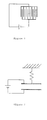
- the sets of inter-digitated fingers shown e.g. in fig.1, shift into each other.
- the movement uses the single degree of freedom available to the system, i.e. the direction of the fingers; in other words the devices move in-plane.
- Parallel-plate capacitors as an electrostatic actuator are also known [ X. Rottenberg et al., RF-MEMS technology platform for agile mobile and satellite communications, Proc. of the 36th European Microwave Conf., pp. 1723-1726, September 2006 ].
- This type of devices is often preferred for on-chip actuators as they only require in principle a few additional thin-film processing steps.
- This type of structures is indeed produced by a typical 4-mask process flow realized on top of a dielectric (insulated) substrate.
- the movable plate or electrode gets nearer to the fixed, bottom electrode one; the device moves out-of-plane as shown e.g. in fig.2, whereby the movable electrode approaches the bottom electrode.
- the electrodes remain in different planes.
- electrostatic devices examples include RF-MEMS switches, switchable capacitors, tilting mirrors, power scavengers, accelerometers ... etc.
- RF-MEMS switches switches, switchable capacitors, tilting mirrors, power scavengers, accelerometers ... etc.
- These prior art devices have the problem that integration of a 4-masks process in/or above another process is rather difficult.
- the dielectric layer is typically sensitive to various charging mechanisms.
- the release process also has a strong impact on the dielectric properties. Often malfunction of clamped-free devices occurs due to the stress-gradient in the armature.
- a three-dimensional variable capacitor is described in US-patent 2005/6906905 .
- the electrodes of the capacitor are formed in an interdigitated manner with movable MEMS comb drive electrode beams. Control or actuation electrodes on the beams drive their motion either individually or all in unison, leading to changes in the capacitance.
- the structure of this variable capacitor is very complex.
- variable capacitor which shows a less complex structure and which is as a result easier to manufacture.
- a variable capacitor comprises first and second electrically conductive electrodes spaced apart from each other and defining the capacitance of the capacitor. At least one of said electrodes comprises at least one bendable portion. The conductive electrodes are arranged above a support structure with the bendable portions being movable perpendicular to the support structure.
- the variable capacitor further comprises an actuation means for actuating each bendable portion to vary the capacitance of said variable capacitor.
- the actuation means comprises a means for generating a DC voltage difference between said electrodes.
- variable capacitor of the present invention uses fringing fields as actuation mechanism. Upon actuation, each of said bendable portions of the electrodes will move in order to maximise the capacitance while minimising its energy.
- variable capacitor of the present invention An analysis of the problem of the prior art variable capacitor has shown that the structure is very complex in view of the fact that actuation of the motion of the movable comb is driven by extra actuation electrodes.
- no extra actuation electrodes need to be implemented, since the bendable portions which are part of the capacitor electrodes are used themselves for actuation.
- the same elements of the variable capacitor are used for actuation and for controlling the capacitance, simplifying the structure severely while maintaining a device which has a large capacitance ratio or tuning range. Because of the simplified structure, the device can be produced in a simple 2-mask process. The simplicity allows a vast flexibility for the processing and as a result strongly eases the integration of such devices into existing technologies.
- the actuation means further comprises a layer within said support structure (103) having a higher permittivity value than the atmosphere surrounding said electrodes.
- the proximity of this layer in the support structure with its higher permittivity produces an unbalance in the electric field distribution between top and bottom faces of the electrodes.
- the unbalance results in a net force, towards the high permittivity support structure.
- the bendable portions configure such that they are pulled towards the support structure. Again, to maximise the capacitance while minimising its energy, the electrodes may come into physical contact with the support structure.
- the electrodes are arranged essentially in the same plane, while the bendable portions are laying out of that plane in idle state, due to their residual stress gradient.
- the bendable portions configure such that they are positioned essentially in said plane.
- each of the electrodes comprises at least one bendable portion.
- the bendable portions are preferably formed by cantilevered structures, having an anchored portion and a free-standing portion.
- the electrodes preferably comprise patterned metal layers.
- the electrodes may further be formed out of the same layer.
- the electrodes comprise sub layers. These sub layers can be made for example of metal, dielectric or piezoelectric. They can also be patterned in order for example to stiffen the electrodes and or tune their spring constant.
- one of said electrodes is completely fixed on said support structure.
- the actuation mechanism will be dominated by the fringing fields' actuation. This has the advantage of lowering the required actuation voltage.
- the support structure is provided with recesses arranged for accepting the bendable portions when actuated. This would allow for example the definition of variable capacitor with fixed stable actuated state without contact with the substrate and the production of large amplitude rotary device with large excursion within the substrate.
- the electrodes are digitated structures, and are arranged such that upon actuation they configure as an interdigitated structure.
- the actuation of the device preferably occurs through the fringing fields, maximizing these is favourable. Interdigitated fingers are most prompt to this actuation principle we use.
- the length of said digitated structures is varied, so that a more progressive tuning can be achieved.
- the support structure may comprise only the high permittivity layer, or be a multilayer structure.
- the support structure comprises an MCM-D substrate.
- variable capacitor based RF devices and circuits are presented. Possible examples are an LC-tank, a relay, a shunt relay capacitor and a series relay capacitor. All applications comprise said variable capacitor.
- the variable capacitor as described in the present invention can also be used as or in a sensor.
- a second aspect of the present invention presents a method for the production of a variable capacitor.
- a method for the production in a 2-mask process of a variable capacitor comprising the steps of:
- the method of patterning the conductive layer further results in the first electrode and the second electrode being interdigitated structures.
- the method further comprises of the step of providing recesses in the support substrate, the recesses being arranged for accepting the bendable portions when actuated.
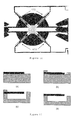
- Fig.1 shows a comb-driven electrostatic device.
- Fig.2 shows a parallel-plate electrostatic device.
- Fig.3 shows a block diagram of the variable capacitor of the present invention.
- Fig.4 shows the top view and cross sections of an interdigitated structure according to the present invention.
- Fig.5 shows schematic the out-of-plane-to-in-plane electrostatic actuation.
- Fig.6 shows the realized device in its (a) idle and (b) actuated states.
- Fig.7 shows schematic the free-standing-to-contacted electrostatic actuation.
- Fig.8 shows an interdigitated example of the present invention in its (a) idle and (b) actuated states.
- Fig.9 shows a typical C-V characteristic of an actuated device.
- Fig.10 shows the cross section of the standard device and its asymmetric embodiment.
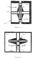
- Fig.11 shows a basic process flow.
- Fig.12 shows a comparison of the measured C-V characteristics of the standard device and its asymmetric embodiment.
- Fig.13 shows some plots of the measured S-parameters of the standard device and its asymmetric embodiment.
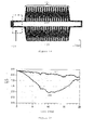
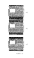
- Fig.14 show a top view microphotograph of a shunt of Electrostatic Fringing Field Actuator (EFFA) RF capacitor.
- EFFA Electrostatic Fringing Field Actuator
- Fig.15 shows a plot of the measured S 21 of an EFFA.
- Fig.16 shows a plot of the C-V characteristics of an EFFA.
- Fig.17 shows top view microphotograph of a series EFFA RF capacitor with additional anchoring at the tips of the fingers.
- Fig.18 shows a plot of the measured C-V of EFFA.
- Fig.19 shows a microphotograph of a processed series LC-tank implementing a fixed spiral inductor and a series EFFA capacitors.
- Fig.20 shows a tunable LC-tank with a variable length series EFFA.
- Fig.21 shows schematic side- and top-views of a shunt relay. On the left: conventional parallel-plate actuator, on the right: EFFA.
- Fig.22 shows a shunt switchable capacitor actuated as a relay by EFFA's beside the signal line.
- Fig.23 shows a series switchable capacitor actuated as a relay by 2 transverse EFFA's.
- Fig.24 shows a shunt capacitive relay implementing 4 EFFA's as side-actuators.
- Fig.25 shows a possible alternative process flow.
- Fig.26 shows a 3D-visualization of a basic variable capacitor.
- Fig.27 shows a 3D-visualization of an asymmetric variable capacitor.
- Fig.28 shows a 3D-visualization of a variable capacitor implementing bridges.
- Fig.29 shows a 3D-visualization of a variable capacitor with locally thickened moving electrodes.
- Fig.30 shows a 3D-visualization of a variable capacitor moving in an underlying cavity.
- Fig.31 shows a 3D-visualization of a variable capacitor moving in an underlying cavity.
- Fig.32 shows a 3D-visualization of a variable capacitor with a fixed thick electrode.
- Fig.33 shows the electric field distribution in the cross section of a unit periodic cell.
- Fig.34 shows a 3D-visualization of a variable capacitor.
- Fig.35 shows the electric field distribution in the cross section of a unit periodic cell.
- the present invention is illustrated in fig.3.
- At least one electrode is arranged such that a portion of the electrode is bendable.
- the electrodes are arranged above a support structure (103).
- the bendable portions are movable in a direction perpendicular to the support structure and not in a direction parallel to this support structure.
- the present invention comprises an actuation means for actuating the bendable portion to vary the capacitance of the variable capacitor.
- the actuation means comprises a means (104) for generating a voltage difference between the conductive electrodes.
- this support structure (103) is typically a substrate with a permittivity value higher than the atmosphere surrounding the electrodes.
- each of the electrodes comprises at least one of the bendable portions.
- the electrodes are arranged essentially in the same plane, while the bendable portions are laying out of that plane due to their residual stress gradient. Upon actuation, a voltage difference is generated between the electrodes and the bendable portions align.
- the bendable portions are cantilevered structures, having an anchored portion (201) and a free-standing portion (202).
- Embodiments according to the present invention are shown in Fig.4. They comprise two sets of movable interdigitated fingers (203) free-standing above the substrate. There is no electrode underneath the fingers. In the idle state, the beams curl out-of-plane as shown in fig.5(a) due to their residual stress gradient, lowering the rest capacitance between the fingers.
- An aspect of the embodiments according to the present invention is the alignment of the fingers.
- a DC-voltage (104) applied between the 2 electrodes produces fringing fields that result in opposite torques working on both sets of fingers as shown in fig.6(a). These tend to align (fig.6(b)) the fingers parallel to each other. This is sketched in fig.6, where straight rigid conductors rotating around their fixed anchors symbolise the fingers. The springs account for the stiffness of the fingers. The uncurling is depicted in fig.5(a) to fig.5(c). By aligning, the fingers maximise their total capacitance.
- the support structure has a higher permittivity value than the surrounding atmosphere as e.g. vacuum, air, gases, oil or other fluids.
- the proximity to the substrate with ⁇ r >1 produces an unbalance of the E-field distribution between top and bottom faces of the fingers.
- Fig.7 shows a cell of the periodic cross-section through the width of the fingers. Because of the symmetry induced by the periodic arrangement of the fingers, an equipotential plane occupies the centre of each slot (fig.7(a)). The total force on each finger is vertical that tends to get both families of fingers to contact the substrate.
- the fields are mainly directed towards the dielectric substrate due to its high relative permittivity ⁇ r .
- fringing-fields actuation principle that has been demonstrated can be used also as an electrostatic sensing mechanism.
- the idle and actuated states of the device are shown in fig.8.
- the tips of the fingers appear dark as they do not reflect the light towards the microscope (fig.8(a)). These are the areas of maximum deflection.
- the fingers flatten on the surface of the substrate and appear uniformly shiny (fig.8(b)).
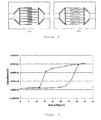
- the corresponding C-V characteristic is shown in fig.9.
- a modified structure has been realized in a similar process flow, where one family of fingers was completely fixed and produced in contact with the substrate (the difference being illustrated in fig.10(a) shows the symmetric embodiment, fig.10(b) shows the asymmetric embodiment).
- the corresponding C-V characteristic is shown in fig.12. Line (301), respectively (302) represents the C-V characteristic of the symmetric embodiment, respectively the asymmetric embodiment.
- the capacitance increases with increasing bias voltage. At the moment the electrodes come in contact with the substrate, "pull-in”, the capacitance increases faster (304). Reversely, the capacitance decreases slowly with a decreasing voltage. At the "pull-out” instance, the capacitance drops (303). At least the following effects can be seen for the asymmetric embodiment, which are illustrated in fig.12:
- the measured transmission parameter i.e. S 21 of both the symmetric (310) and the asymmetric (320) devices in rest (340) and in actuated (330) states are plotted in fig.13.
- Fig.13(a) shows the amplitudes and fig.13(b) the phase of the measured transmission parameter.
- further modifications of the capacitance ratio can be realized by changing for instance (1) the design, e.g. the length/width/spacing of the fingers,(2) the substrate, the layered substrate, and (3) the ambience or environment, the gas/fluid, e.g. oil.
- the essence is to use the fact that the fringing fields go through the dielectric or insulated substrate for the actuation.
- Cantilever beams are also not really needed.
- a foot may be for example placed at the end of the beams, hereby creating bridge-type structures in order not to rely on the reproducibility of the stress gradient in the beams. In the idle state the beams will not curl out of plane.
- Embodiments according to the present invention have the advantage that they can essentially be produced by a two mask process (a. sacrificial layer (120) and b. movable and/or fixed electrode (130)).
- a single metal layer and mask can be used for forming the capacitor electrodes.
- no dielectric layer is necessary except for the one to insulate the substrate.
- the present invention can be implemented to obtain a novel electrostatic actuator.
- This actuator uses fringing fields as actuation mechanism, Electrostatic Fringing Field Actuator, EFFA.
- EFFA Electrostatic Fringing Field Actuator
- Electrostatic Fringing-Field Actuators used as variable capacitors have been demonstrated in various embodiments.
- Fig.14 shows a microphotograph of a shunt EFFA-based capacitor for RF-applications.
- (401) represents an interdigitated EFFA capacitor
- (402) is the RF signal line
- (403) is the RF ground plane
- (404) shows the RF probing area. Its measured S 21 is plotted in fig. 15, for the idle-state (501) and the actuated state (502).
- the EFFA variable capacitors have been accommodated for RF-measurement using a second metallisation.
- BCB benzocyclobutene
- floating anchors (701) at the tips of the fingers are added, as shown in fig. 17. These floating anchors mitigate the effect of the stress gradient on the free-standing beams.
- the capacitance contrast between idle and actuated states is only due to the contact with the substrate.
- a second metallization In another embodiment, the implementation of a second metallization is described. It allows defining the underpass of spiral inductors (802) used in tuneable LC-tanks (801) shown in fig.19.
- variable LC-tank with variable length series EFFA (901) is presented, see fig.20.
- the length of the fingers was varied within the same EFFA to allow a progressive frequency tuning and not only a switching.
- Parallel-plate capacitors (1003) can be implemented as EFFA-based relays to define either ohmic relays or high capacitance ratio relays.
- a conventional implementation of an electrostatic relay is depicted in fig.21(a).
- a parallel-plate actuator (1003) with a fixed electrode (1002) is defined under a grounded bridge (1001), away from the central RF-contact (1004) area. The RF-contact (1004) closes.
- the fixed electrode (1002) is coated to prevent any DC-short during the actuation.
- the parallel-plate actuator (1003) is replaced by an EFFA (401).
- the RF-structure is anchored through 2 grounded legs interdigitated with an actuation finger (1005), e.g. clamped-free in this case.
- an actuation finger (1005) e.g. clamped-free in this case.
- the hot finger (1005) Upon actuation of a bias to the hot finger (1005), the legs and hot finger contact in the substrate, closing as a result the RF-contact (1004).
- FIG.22 An example of a shunt relay is depicted in fig.22 A moving electrode overlaps with the signal line of a CPW. It is in this case anchored in the ground through 4 legs interdigitated with 3 actuation fingers (2001) biased through 1 separate DC pad (2003).
- the DC voltage drop between top and bottom electrodes of the RF capacitor is nil.
- the device defines a capacitance limited by the native AlO x thickness and the contact quality between the electrodes. The measured capacitance ratio of this device is reached 1:7.
- a series tuneable capacitor (3003) can be designed, fig. 23.
- Transverse restraining bridges at the tip of the cantilever lower the impact of the stress gradient on the idle-capacitance definition. They further allow designing 2 transverse EFFA's (401) with the addition of actuation fingers. In the present case, RF-grounded beams interdigitated with the transverse beams are used. At low frequency, the EFFA capacitance is small enough to isolate the signal line from the ground planes while providing an efficient actuation mechanism.
- the device is thus actuated by biasing both signal lines versus the ground planes. It is thus not a relay in the sense that DC-and RF-signals are superposed but well in the sense that the actuation is separated from the sensing, i.e. the RF-functionality.
- a shunt capacitive relay can be based on the design of the device of fig.22, see fig. 24. It is designed to present shunt switching characteristics, e.g. low insertion loss in idle-state and high isolation in actuated-state.
- the large top electrode is spun between 4 double legs constituting the grounded parts of 4 EFFA's (401).
- the hot fingers of the actuators are either clamped-free beams or fixed stripes processed in contact with the substrate to lower the actuation voltage.
- the processing steps used and described previously are only indicative.
- the sputtering of the Al layer can be replaced for example by the plating of another metal while polyimide, along with a wide variety of other materials, can be used as a sacrificial layer.
- the asymmetric embodiment is presented in fig.27 where the finger set on the right lies on the substrate.
- the device can be uniformly or locally stiffened by thickening the electrodes. This is sketched in fig.29.
- a further embodiment is presented in fig.30 where the fingers move downwards in an underlying cavity.
- one electrode or set of fingers is made thicker than the other and processed directly on the substrate. This modifies the evolution of the capacitance and electrostatic force on the moving electrode during its displacement as sketched in fig.33 Depending on the thickness of the electrodes, the relative permittivity of the substrate and the design parameters, like the spacing between the fingers, a stable actuated state can be produced without contacting the substrate.
- Fig.35 shows the evolution of the electric field distribution around the electrodes in this case during the displacement of the moving portions.
Landscapes
- Engineering & Computer Science (AREA)
- Power Engineering (AREA)
- Microelectronics & Electronic Packaging (AREA)
- Fixed Capacitors And Capacitor Manufacturing Machines (AREA)
- Micromachines (AREA)
- Semiconductor Integrated Circuits (AREA)
Priority Applications (4)
| Application Number | Priority Date | Filing Date | Title |
|---|---|---|---|
| EP20070113726 EP1890306B1 (fr) | 2006-08-18 | 2007-08-02 | Condensateur variable à MEMS et son procédé de fabrication |
| DE602007011009T DE602007011009D1 (de) | 2006-08-18 | 2007-08-02 | Variabler MEMS-Kondensator und Verfahren zu seiner Herstellung |
| AT07113726T ATE491216T1 (de) | 2006-08-18 | 2007-08-02 | Variabler mems-kondensator und verfahren zu seiner herstellung |
| US11/893,990 US7782594B2 (en) | 2006-08-18 | 2007-08-17 | MEMS variable capacitor and method for producing the same |
Applications Claiming Priority (1)
| Application Number | Priority Date | Filing Date | Title |
|---|---|---|---|
| US83876806P | 2006-08-18 | 2006-08-18 |
Publications (1)
| Publication Number | Publication Date |
|---|---|
| EP1890305A1 true EP1890305A1 (fr) | 2008-02-20 |
Family
ID=37963636
Family Applications (1)
| Application Number | Title | Priority Date | Filing Date |
|---|---|---|---|
| EP07102351A Withdrawn EP1890305A1 (fr) | 2006-08-18 | 2007-02-14 | Condensateur variable MEMS et son procédé de fabrication |
Country Status (3)
| Country | Link |
|---|---|
| EP (1) | EP1890305A1 (fr) |
| AT (1) | ATE491216T1 (fr) |
| DE (1) | DE602007011009D1 (fr) |
Cited By (1)
| Publication number | Priority date | Publication date | Assignee | Title |
|---|---|---|---|---|
| AT516662A1 (de) * | 2014-12-12 | 2016-07-15 | Next System Vertriebsges M B H | Haptisches Feedback-Element eines Eingabeelements für elektronische Apparate |
Citations (9)
| Publication number | Priority date | Publication date | Assignee | Title |
|---|---|---|---|---|
| WO1997001221A1 (fr) * | 1995-06-23 | 1997-01-09 | Cornell Research Foundation, Inc. | Resonateurs micromecaniques accordables de type capacitif |
| WO2001045127A1 (fr) * | 1999-12-15 | 2001-06-21 | Mcnc | Condensateur variable a commande electrostatique |
| US6290510B1 (en) * | 2000-07-27 | 2001-09-18 | Xerox Corporation | Spring structure with self-aligned release material |
| WO2002079076A1 (fr) * | 2001-03-30 | 2002-10-10 | Jds Uniphase Corporation | Elements de dispositifs de systemes mecaniques microelectriques possedant des parties en contact avec un substrat et procedes de fonctionnement associes |
| US6625004B1 (en) * | 2001-08-31 | 2003-09-23 | Superconductor Technologies, Inc. | Electrostatic actuators with intrinsic stress gradient |
| WO2004080886A1 (fr) * | 2003-03-13 | 2004-09-23 | Btg International Limited | Dispositifs a systemes mecaniques microelectriques (mems) a echelle nanometrique |
| US20050013087A1 (en) * | 2003-05-21 | 2005-01-20 | The Regents Of The University Of California | MEMS tunable capacitor based on angular vertical comb drives |
| EP1536439A1 (fr) * | 2003-11-25 | 2005-06-01 | St Microelectronics S.A. | Composant incluant un condensateur variable |
| US6906905B1 (en) * | 2004-06-30 | 2005-06-14 | International Business Machines Corporation | Micro electro-mechanical variable capacitor |
-
2007
- 2007-02-14 EP EP07102351A patent/EP1890305A1/fr not_active Withdrawn
- 2007-08-02 DE DE602007011009T patent/DE602007011009D1/de active Active
- 2007-08-02 AT AT07113726T patent/ATE491216T1/de not_active IP Right Cessation
Patent Citations (9)
| Publication number | Priority date | Publication date | Assignee | Title |
|---|---|---|---|---|
| WO1997001221A1 (fr) * | 1995-06-23 | 1997-01-09 | Cornell Research Foundation, Inc. | Resonateurs micromecaniques accordables de type capacitif |
| WO2001045127A1 (fr) * | 1999-12-15 | 2001-06-21 | Mcnc | Condensateur variable a commande electrostatique |
| US6290510B1 (en) * | 2000-07-27 | 2001-09-18 | Xerox Corporation | Spring structure with self-aligned release material |
| WO2002079076A1 (fr) * | 2001-03-30 | 2002-10-10 | Jds Uniphase Corporation | Elements de dispositifs de systemes mecaniques microelectriques possedant des parties en contact avec un substrat et procedes de fonctionnement associes |
| US6625004B1 (en) * | 2001-08-31 | 2003-09-23 | Superconductor Technologies, Inc. | Electrostatic actuators with intrinsic stress gradient |
| WO2004080886A1 (fr) * | 2003-03-13 | 2004-09-23 | Btg International Limited | Dispositifs a systemes mecaniques microelectriques (mems) a echelle nanometrique |
| US20050013087A1 (en) * | 2003-05-21 | 2005-01-20 | The Regents Of The University Of California | MEMS tunable capacitor based on angular vertical comb drives |
| EP1536439A1 (fr) * | 2003-11-25 | 2005-06-01 | St Microelectronics S.A. | Composant incluant un condensateur variable |
| US6906905B1 (en) * | 2004-06-30 | 2005-06-14 | International Business Machines Corporation | Micro electro-mechanical variable capacitor |
Cited By (2)
| Publication number | Priority date | Publication date | Assignee | Title |
|---|---|---|---|---|
| AT516662A1 (de) * | 2014-12-12 | 2016-07-15 | Next System Vertriebsges M B H | Haptisches Feedback-Element eines Eingabeelements für elektronische Apparate |
| AT516662B1 (de) * | 2014-12-12 | 2018-06-15 | Next System Vertriebsges M B H | Haptisches Feedback-Element eines Eingabeelements für elektronische Apparate |
Also Published As
| Publication number | Publication date |
|---|---|
| DE602007011009D1 (de) | 2011-01-20 |
| ATE491216T1 (de) | 2010-12-15 |
Similar Documents
| Publication | Publication Date | Title |
|---|---|---|
| US7782594B2 (en) | MEMS variable capacitor and method for producing the same | |
| Mahameed et al. | Dual-beam actuation of piezoelectric AlN RF MEMS switches monolithically integrated with AlN contour-mode resonators | |
| Yao et al. | High tuning ratio MEMS based tunable capacitors for RF communications applications | |
| US7265019B2 (en) | Elastomeric CMOS based micro electromechanical varactor | |
| US6074890A (en) | Method of fabricating suspended single crystal silicon micro electro mechanical system (MEMS) devices | |
| EP2497189B1 (fr) | Filtre pouvant être accordé basé sur un microsystème électromécanique | |
| US20050270128A1 (en) | Switch | |
| US7977136B2 (en) | Microelectromechanical systems structures and self-aligned high aspect-ratio combined poly and single-crystal silicon fabrication processes for producing same | |
| US20070236307A1 (en) | Methods and apparatus for a packaged MEMS switch | |
| FI127231B (fi) | Mikrosähkömekaaninen kytkinkokoonpano ja menetelmä mikrosähkömekaanisen kytkinkokoonpanon valmistamiseksi | |
| US7439117B2 (en) | Method for designing a micro electromechanical device with reduced self-actuation | |
| WO2002059921A1 (fr) | Dispositif micromecanique a coefficient q eleve et son procede de reglage | |
| Rottenberg et al. | An electrostatic fringing-field actuator (EFFA): application towards a low-complexity thin-film RF-MEMS technology | |
| Pu et al. | Stable zipping RF MEMS varactors | |
| US9070524B2 (en) | RF MEMS switch with a grating as middle electrode | |
| EP1890305A1 (fr) | Condensateur variable MEMS et son procédé de fabrication | |
| EP1890306B1 (fr) | Condensateur variable à MEMS et son procédé de fabrication | |
| Sinha et al. | Dual beam actuation of piezoelectric AlN RF MEMS switches integrated with AlN contour-mode resonators | |
| McFeetors et al. | Performance and operation of stressed dual-gap RF MEMS varactors | |
| Reinke | CMOS-MEMS variable capacitors for reconfigurable RF circuits | |
| Rottenberg et al. | Novel EFFA-based thin-film RF-MEMS technology | |
| Small et al. | Electrostatically tunable analog single crystal silicon fringing-field MEMS varactors | |
| Rahman et al. | Low actuation voltage RF MEMS series switch with novel beam design | |
| Rottenberg et al. | Electrostatic fringing-field actuator (EFFA): Application towards a low-complexity RF-MEMS technology | |
| Lee et al. | Surface micromachined GHz tunable capacitor with 14: 1 continuous tuning range |
Legal Events
| Date | Code | Title | Description |
|---|---|---|---|
| PUAI | Public reference made under article 153(3) epc to a published international application that has entered the european phase |
Free format text: ORIGINAL CODE: 0009012 |
|
| AK | Designated contracting states |
Kind code of ref document: A1 Designated state(s): AT BE BG CH CY CZ DE DK EE ES FI FR GB GR HU IE IS IT LI LT LU LV MC NL PL PT RO SE SI SK TR |
|
| AX | Request for extension of the european patent |
Extension state: AL BA HR MK YU |
|
| AKX | Designation fees paid | ||
| REG | Reference to a national code |
Ref country code: DE Ref legal event code: 8566 |
|
| STAA | Information on the status of an ep patent application or granted ep patent |
Free format text: STATUS: THE APPLICATION IS DEEMED TO BE WITHDRAWN |
|
| 18D | Application deemed to be withdrawn |
Effective date: 20080821 |