EP1887368A1 - Circuit and method for determining potentionmeter wiper resistance - Google Patents
Circuit and method for determining potentionmeter wiper resistance Download PDFInfo
- Publication number
- EP1887368A1 EP1887368A1 EP07113842A EP07113842A EP1887368A1 EP 1887368 A1 EP1887368 A1 EP 1887368A1 EP 07113842 A EP07113842 A EP 07113842A EP 07113842 A EP07113842 A EP 07113842A EP 1887368 A1 EP1887368 A1 EP 1887368A1
- Authority
- EP
- European Patent Office
- Prior art keywords
- potentiometer
- terminal
- wiper
- resistance
- coupled
- Prior art date
- Legal status (The legal status is an assumption and is not a legal conclusion. Google has not performed a legal analysis and makes no representation as to the accuracy of the status listed.)
- Withdrawn
Links
- 238000000034 method Methods 0.000 title claims abstract description 22
- 230000008878 coupling Effects 0.000 claims abstract description 4
- 238000010168 coupling process Methods 0.000 claims abstract description 4
- 238000005859 coupling reaction Methods 0.000 claims abstract description 4
- 238000005259 measurement Methods 0.000 claims description 5
- 101100091492 Rattus norvegicus Rorb gene Proteins 0.000 description 7
- 238000012986 modification Methods 0.000 description 3
- 230000004048 modification Effects 0.000 description 3
- 230000004044 response Effects 0.000 description 3
- 238000011065 in-situ storage Methods 0.000 description 2
- 230000008569 process Effects 0.000 description 2
- 230000007423 decrease Effects 0.000 description 1
- 238000010586 diagram Methods 0.000 description 1
- 230000007613 environmental effect Effects 0.000 description 1
Images


Classifications
-
- G—PHYSICS
- G01—MEASURING; TESTING
- G01D—MEASURING NOT SPECIALLY ADAPTED FOR A SPECIFIC VARIABLE; ARRANGEMENTS FOR MEASURING TWO OR MORE VARIABLES NOT COVERED IN A SINGLE OTHER SUBCLASS; TARIFF METERING APPARATUS; MEASURING OR TESTING NOT OTHERWISE PROVIDED FOR
- G01D5/00—Mechanical means for transferring the output of a sensing member; Means for converting the output of a sensing member to another variable where the form or nature of the sensing member does not constrain the means for converting; Transducers not specially adapted for a specific variable
- G01D5/12—Mechanical means for transferring the output of a sensing member; Means for converting the output of a sensing member to another variable where the form or nature of the sensing member does not constrain the means for converting; Transducers not specially adapted for a specific variable using electric or magnetic means
- G01D5/14—Mechanical means for transferring the output of a sensing member; Means for converting the output of a sensing member to another variable where the form or nature of the sensing member does not constrain the means for converting; Transducers not specially adapted for a specific variable using electric or magnetic means influencing the magnitude of a current or voltage
- G01D5/16—Mechanical means for transferring the output of a sensing member; Means for converting the output of a sensing member to another variable where the form or nature of the sensing member does not constrain the means for converting; Transducers not specially adapted for a specific variable using electric or magnetic means influencing the magnitude of a current or voltage by varying resistance
- G01D5/165—Mechanical means for transferring the output of a sensing member; Means for converting the output of a sensing member to another variable where the form or nature of the sensing member does not constrain the means for converting; Transducers not specially adapted for a specific variable using electric or magnetic means influencing the magnitude of a current or voltage by varying resistance by relative movement of a point of contact or actuation and a resistive track
-
- G—PHYSICS
- G01—MEASURING; TESTING
- G01R—MEASURING ELECTRIC VARIABLES; MEASURING MAGNETIC VARIABLES
- G01R27/00—Arrangements for measuring resistance, reactance, impedance, or electric characteristics derived therefrom
- G01R27/02—Measuring real or complex resistance, reactance, impedance, or other two-pole characteristics derived therefrom, e.g. time constant
- G01R27/20—Measuring earth resistance; Measuring contact resistance, e.g. of earth connections, e.g. plates
- G01R27/205—Measuring contact resistance of connections, e.g. of earth connections
-
- G—PHYSICS
- G01—MEASURING; TESTING
- G01R—MEASURING ELECTRIC VARIABLES; MEASURING MAGNETIC VARIABLES
- G01R31/00—Arrangements for testing electric properties; Arrangements for locating electric faults; Arrangements for electrical testing characterised by what is being tested not provided for elsewhere
- G01R31/28—Testing of electronic circuits, e.g. by signal tracer
- G01R31/282—Testing of electronic circuits specially adapted for particular applications not provided for elsewhere
- G01R31/2829—Testing of circuits in sensor or actuator systems
Definitions
- the present invention relates to potentiometer characteristic measurement and, more particularly, to a circuit and method for determining the wiper resistance of a potentiometer.
- a potentiometer is an electronic component that is configured to provide a user-adjustable resistance.
- the potentiometer is a three-terminal circuit element that includes first, second, and third terminals, a resistor electrically coupled between the first and second terminals, and a wiper electrically coupled between the resistor and the third terminal. The wiper is movable along the resistor, thereby providing a variable resistance between the wiper terminal and each of the first and second terminals.
- Potentiometers are used in myriad devices and systems. For example, potentiometers are many times used to supply signals representative of the position of various components. Such components may include various types of valves, actuators, or various mechanical devices. As is generally known, the resistance of a potentiometer's terminals, as well as the resistance of the potentiometer wiper, may vary over time. These resistances may also vary with various environmental conditions to which the potentiometer may be exposed. Hence, various devices and methods have been developed to determine, in-situ, potentiometer resistances, including potentiometer wiper resistance.
- the present invention provides a circuit and method for determining potentiometer wiper resistance.
- a method of determining the wiper resistance of a potentiometer that includes a first terminal, a second terminal, a third terminal, a resistive element having a potentiometer resistance electrically coupled between the first and second terminals, and a wiper electrically coupled between the resistive element and the third terminal and movable to a wiper position between the first and second terminals, includes the step of electrically coupling a sense resistor having a substantially constant sense resistance to the potentiometer third terminal.
- the potentiometer is electrically energized, and a potentiometer voltage is determined.
- the potentiometer voltage being a voltage potential between the potentiometer first and second terminals.
- the wiper position is determined based at least in part on the determined potentiometer voltage.
- the sense resistor is electrically coupled to a potential that causes a wiper current to flow through the wiper and sense resistor.
- a magnitude of the wiper current is determined, and the wiper resistance is determined based at least in part on the potentiometer resistance, the determined potentiometer position, the determined wiper current magnitude, and the sense resistance.
- a potentiometer wiper resistance measurement circuit includes a potentiometer, a sense resistor, a power source, and an output circuit.
- the potentiometer includes a first terminal, a second terminal, a third terminal, a resistive element having a potentiometer resistance electrically coupled between the first and second terminals, and a wiper electrically coupled between the resistive element and the third terminal and movable to a wiper position between the first and second terminals.
- the sense resistor has a substantially constant sense resistance and includes a first terminal and a second terminal. The sense resistor first terminal is coupled to the potentiometer third terminal.
- the power source is electrically coupled to the potentiometer and is configured to supply a current thereto that results in a voltage drop between the potentiometer first and second terminals.
- the output circuit has a plurality of input terminals and an output terminal. Separate ones of the output circuit input terminals are coupled to at least the potentiometer first terminal, the potentiometer second terminal, and the sense resistor output terminal. The output circuit operable to selectively couple the potentiometer first terminal to the output terminal, the potentiometer third terminal to the output terminal, and the sense resistor second terminal to a reference potential.
- a potentiometer wiper resistance measurement circuit includes a potentiometer, a sense resistor, a power source, and first, second, third, and fourth multiplexers.
- the potentiometer includes a first terminal, a second terminal, a third terminal, a resistive element having a potentiometer resistance electrically coupled between the first and second terminals, and a wiper electrically coupled between the resistive element and the third terminal and movable to a wiper position between the first and second terminals.
- the sense resistor has a substantially constant sense resistance and includes a first terminal and a second terminal. The sense resistor first terminal is coupled to the potentiometer third terminal.
- the power source is electrically coupled to the potentiometer and is configured to supply a current thereto that results in a voltage drop between the potentiometer first and second terminals.
- the first multiplexer has a plurality of input terminals and an output terminal. A first of its input terminals is coupled to the potentiometer first terminal, and a second of its input terminals coupled to the potentiometer third terminal.
- the second multiplexer has a plurality of input terminals and an output terminal. A first of its input terminals is coupled to the sense resistor second terminal.
- the third multiplexer has a plurality of input terminals and an output terminal. A first of its input terminals is coupled to the reference potential, and its output terminal is coupled to the second multiplexer output terminal.
- the fourth multiplexer has a plurality of input terminals and an output terminal. A first of its input terminals is coupled to the first multiplexer output terminal, and a second of its input terminals is coupled to the second multiplexer output terminal.
- FIG. 1 depicts a functional block diagram of a potentiometer and exemplary circuit that may be used to determine the wiper resistance of the potentiometer
- FIG. 2 depicts an exemplary process, in flowchart from, that may be implemented by the circuit of FIG. 1 for determining the potentiometer wiper resistance.
- the circuit 100 includes a potentiometer 102, a sense resistor 104, and an output circuit 106.
- the potentiometer 102 includes a first terminal 108-1, a second terminal 108-2, a third terminal 108-3, a resistive element 110, and a wiper 112.
- the resistive element 110 is coupled between the first and second terminals 108-1, 108-2, and has a substantially constant resistance, which is referred to herein as the potentiometer resistance (R pot ) .
- R pot potentiometer resistance
- the resistive element 110 may be implemented using any one of numerous types of electrically resistive devices, and may additionally be implemented using one or more circuit elements.
- the first terminal 108-1 is coupled to a voltage source 114, and the second terminal 108-2 is coupled to a reference potential, such as circuit common.
- a current flows through the resistive element 110, generating a voltage drop across the resistive element 110.
- the first terminal 108-1 is coupled to the voltage source 114via one or more current limiting resistors 116, and the second terminal 108-2 is coupled to the reference potential via one or more bias resistors 117.
- this configuration is merely exemplary, and that the potentiometer first terminal 108-1 and/or the second terminal 108-2 could instead be directly coupled to the voltage source 114 and the reference potential, respectively.
- the potentiometer resistance (R pot ) is unknown, or could vary with, for example, time and/or temperature, then the one or more current limiting resistors 116 are preferably included. If, however, the potentiometer resistance (R pot ) is known, the one or more current limiting resistors 116 could be omitted.
- the wiper 112 is electrically coupled between the resistive element 110 and the third terminal 108-3, and is movable to a position between the first and second terminals 108-1, 108-2.
- the resistance between the third terminal 108-3 and each of the first and second terminals 108-1, 108-2 varies based on the position of the wiper 112.
- the voltage potential at the third terminal 108-3 similarly varies based on the position of the wiper 112. It may be appreciated that, at least in the depicted embodiment, as the wiper 112 is moved closer to the first terminal 108-1, the voltage potential at the third terminal 108-3 increases, and as the wiper 112 is moved closer to the second terminal 108-2, the voltage potential on the third terminal 108-3 decreases.
- the resistance of the wiper may vary over time. As such, the wiper 112 is depicted in FIG. 1 using the schematic symbol for a resistor.
- the sense resistor 104 has a first terminal 118-1, which is electrically coupled to the potentiometer third terminal 108-3, and a second terminal 118-2, which is electrically coupled to the output circuit 106.
- the sense resistor 104 may be implemented using one or more resistors, or various other resistive circuit elements.
- the sense resistor 104 preferably has at least a substantially constant electrical resistance, which is referred to herein as the sense resistance (R sense ).
- the output circuit 106 has a plurality of input terminals 122, and an output terminal 124.
- three of the input terminals 122 are coupled to the potentiometer 102, one of the input terminals 122 is coupled to the sense resistor second terminal 118-2, one of the input terminals 122 is coupled to the reference potential, and one or more of the remaining input terminals 122 are coupled to receive various signals from one or more non-illustrated circuits.
- one of the input terminals 122 is coupled to the potentiometer first terminal 108-1
- another input terminal 122 is coupled to the potentiometer second terminal 108-2
- yet another of the input terminals 122 is coupled to the potentiometer third terminal 108-3.
- the input terminal 122 that is coupled to the potentiometer second terminal 108-2 can be omitted.
- the output circuit 106 also receives one or more input select commands from, for example, a processor 126. In response to the input select commands, the output circuit 106 supplies various signals to its output terminal 124 for further processing.
- the processor 126 that supplies the input select commands is also coupled to the output circuit output terminal 124.
- the processor 126 selectively receives the various signals supplied from to the output circuit output terminal 124 in response to the input select commands supplied to the output circuit 106 from the processor 126.
- separate processors or devices could be used to supply the input select commands and selectively receive the signals supplied from the output circuit 106.
- At least some of the input select commands supplied to the output circuit 106 are used to electrically couple selected ones of the potentiometer terminals 108 to the output circuit output terminal 124, and the sense resistor second terminal 118-2 to the output circuit output terminal 124 and/or to the reference potential. In doing so, the signals at these terminals, which are concomitantly supplied to the output circuit output terminal 124, are used by the processor 126 to determine the potentiometer wiper resistance (R w ). The manner in which the potentiometer wiper resistance (R w ) is determined based on these signals is described below. Before doing so, however, a particular physical implementation of the output circuit 106, which is also depicted in more detail in FIG. 1, will first be described.
- the output circuit includes four multiplexers - a first multiplexer 128, a second multiplexer 132, a third multiplexer 134, and a fourth multiplexer 136 - an analog-to-digital converter (ADC) 138, and may optionally include a gain stage 142.
- Each of the multiplexers 128-136 is a multichannel multiplexer that includes a plurality of channel select input terminals 144, a plurality of input terminals 146, and an output terminal 148. It will be appreciated that the multiplexers 128-136 could be implemented using multiplexers having any one of numerous channels.
- each multiplexer 128-136 could be an N-channel multiplexer that includes log 2 (N) channel select input terminals 144, and N-number of input terminals 146.
- the multiplexers 128-132 are each coupled to receive, via its channel select input terminals 144, selected ones of the input select commands from the processor.
- the multiplexers 128-132 in a conventionally known manner, selectively enables one or more of its input terminals 146, which electrically couples the enabled input terminal 146 to its output terminal 148.
- the ADC 138 is coupled to receive the analog signals supplied to the fourth multiplexer output terminal 148 and, upon receipt thereof, converts the signal, in a conventional manner, to a digital signal for use by the processor 126.
- the gain stage 142 if included, is disposed between the fourth multiplexer 136 and the ADC 138, and amplifies the analog signals supplied from the fourth multiplexer 136 before supplying it to the ADC 138.
- V pot which is defined herein as the voltage potential between the potentiometer first and second terminals, is determined (202).
- this is accomplished by enabling the input terminal 146 of the first multiplexer 128 that is coupled to the potentiometer first terminal 108-1, and the input terminal 146 of the fourth multiplexer 136 that is coupled to the first multiplexer output terminal 148 to measure the voltage potential at the potentiometer first terminal 108-1 (e.g., V HIGH ), and then enabling the input terminal 146 of the third multiplexer 134 that is coupled to the potentiometer second terminal 108-2, and the input terminal 146 of the fourth multiplexer 136 that is coupled to the third multiplexer output terminal 148 to measure the voltage potential at the potentiometer second terminal 108-2 (e.g., V LOW ).
- the wiper voltage (V wiper ) is measured by enabling the input terminal 146 of the second multiplexer 132 that is coupled to the sense resistor second terminal 118-2, and the input terminal 146 of the fourth multiplexer 136 that is coupled to the second multiplexer output terminal 148.
- the input impedance of the gain stage 142 if included, is sufficiently high that the sum of the resistance of the sense resistor 104 (R sense ) and wiper resistance (R w ) has an insigificant impact on the wiper voltage (V wiper ) measurement.
- the sense resistor second terminal 118-2 is coupled to the reference potential, causing a wiper current (I w ) to flow through the wiper 112 and the sense resistor 104 (206). The magnitude of the wiper current is then determined (208).
- the wiper current (I w ) is caused to flow and is measured by simultaneously enabling the input terminal 146 of the first multiplexer 128 that is coupled to the potentiometer third terminal 108-3, the input terminal 146 of the second multiplexer 132 that is coupled to the sense resistor second terminal 118-2, the input terminal 146 of the third multiplexer 134 that is coupled to the reference potential, and the input terminal 146 of the fourth multiplexer 136 that is coupled to the first multiplexer 128 output terminal 148.
- the processor 126 determines the wiper resistance (R w ) based, at least in part, on the potentiometer resistance (R pot ) and the sense resistance (R sense ), both of which are known, the determined potentiometer position (P wiper ), and the determined wiper current (I w ) (212). It will be appreciated that the processor 126 could determine the wiper resistance (R w ) using the known, measured, and determined quantities in accordance with any one of numerous processes, algorithms, or formulae. In a particular preferred embodiment, however, the processor 126 uses a particular formula, which will now be described in more detail.
- the potentiometer resistance (R pot ) includes a first resistance (R x ) and a second resistance (R y ).
- the first resistance (R x ) is the resistance between the first potentiometer terminal 108-1 and the portion of the wiper 112 that contacts the potentiometer resistor 110, which is referred to herein as the wiper contact 108-4.
- the second resistance (R y ) is the resistance between the potentiometer second terminal 108-2 and the wiper contact 108-4.
- V w ⁇ c I w ⁇ R w + R sense
- Vw ⁇ c V ref ⁇ RzRb Rz + Rb Ra + RzRb Rz + Rb
- RzRb Rz + Rb is the parallel resistance formed by R z and R b
- V ref is the voltage source 114.
- IwRz V ref ⁇ RzRb Rz + Rb Ra + RzRb Rz + Rb .
Landscapes
- Physics & Mathematics (AREA)
- General Physics & Mathematics (AREA)
- Electromagnetism (AREA)
- Engineering & Computer Science (AREA)
- General Engineering & Computer Science (AREA)
- Transmission And Conversion Of Sensor Element Output (AREA)
- Measurement Of Resistance Or Impedance (AREA)
- Measuring Instrument Details And Bridges, And Automatic Balancing Devices (AREA)
Abstract
Description
- The present invention relates to potentiometer characteristic measurement and, more particularly, to a circuit and method for determining the wiper resistance of a potentiometer.
- A potentiometer is an electronic component that is configured to provide a user-adjustable resistance. Typically, the potentiometer is a three-terminal circuit element that includes first, second, and third terminals, a resistor electrically coupled between the first and second terminals, and a wiper electrically coupled between the resistor and the third terminal. The wiper is movable along the resistor, thereby providing a variable resistance between the wiper terminal and each of the first and second terminals.
- Potentiometers are used in myriad devices and systems. For example, potentiometers are many times used to supply signals representative of the position of various components. Such components may include various types of valves, actuators, or various mechanical devices. As is generally known, the resistance of a potentiometer's terminals, as well as the resistance of the potentiometer wiper, may vary over time. These resistances may also vary with various environmental conditions to which the potentiometer may be exposed. Hence, various devices and methods have been developed to determine, in-situ, potentiometer resistances, including potentiometer wiper resistance.
- Although the presently known devices and methods for determining potentiometer wiper resistance generally work well, the devices and methods can suffer certain drawbacks. For example, many devices and methods may rely on relatively complex circuitry, or relatively complex and/or expensive circuit modifications, in order to provide in-situ potentiometer wiper resistance determination. Hence, there is a need for a circuit and method of determining wiper resistance that does not rely on relatively complex circuitry, and/or relatively complex and/or expensive circuit modifications. The present invention addresses at least this need.
- The present invention provides a circuit and method for determining potentiometer wiper resistance. In one embodiment, and by way of example only, a method of determining the wiper resistance of a potentiometer that includes a first terminal, a second terminal, a third terminal, a resistive element having a potentiometer resistance electrically coupled between the first and second terminals, and a wiper electrically coupled between the resistive element and the third terminal and movable to a wiper position between the first and second terminals, includes the step of electrically coupling a sense resistor having a substantially constant sense resistance to the potentiometer third terminal. The potentiometer is electrically energized, and a potentiometer voltage is determined. The potentiometer voltage being a voltage potential between the potentiometer first and second terminals. The wiper position is determined based at least in part on the determined potentiometer voltage. The sense resistor is electrically coupled to a potential that causes a wiper current to flow through the wiper and sense resistor. A magnitude of the wiper current is determined, and the wiper resistance is determined based at least in part on the potentiometer resistance, the determined potentiometer position, the determined wiper current magnitude, and the sense resistance.
- In another exemplary embodiment, a potentiometer wiper resistance measurement circuit includes a potentiometer, a sense resistor, a power source, and an output circuit. The potentiometer includes a first terminal, a second terminal, a third terminal, a resistive element having a potentiometer resistance electrically coupled between the first and second terminals, and a wiper electrically coupled between the resistive element and the third terminal and movable to a wiper position between the first and second terminals. The sense resistor has a substantially constant sense resistance and includes a first terminal and a second terminal. The sense resistor first terminal is coupled to the potentiometer third terminal. The power source is electrically coupled to the potentiometer and is configured to supply a current thereto that results in a voltage drop between the potentiometer first and second terminals. The output circuit has a plurality of input terminals and an output terminal. Separate ones of the output circuit input terminals are coupled to at least the potentiometer first terminal, the potentiometer second terminal, and the sense resistor output terminal. The output circuit operable to selectively couple the potentiometer first terminal to the output terminal, the potentiometer third terminal to the output terminal, and the sense resistor second terminal to a reference potential.
- In yet another exemplary embodiment, a potentiometer wiper resistance measurement circuit includes a potentiometer, a sense resistor, a power source, and first, second, third, and fourth multiplexers. The potentiometer includes a first terminal, a second terminal, a third terminal, a resistive element having a potentiometer resistance electrically coupled between the first and second terminals, and a wiper electrically coupled between the resistive element and the third terminal and movable to a wiper position between the first and second terminals. The sense resistor has a substantially constant sense resistance and includes a first terminal and a second terminal. The sense resistor first terminal is coupled to the potentiometer third terminal. The power source is electrically coupled to the potentiometer and is configured to supply a current thereto that results in a voltage drop between the potentiometer first and second terminals. The first multiplexer has a plurality of input terminals and an output terminal. A first of its input terminals is coupled to the potentiometer first terminal, and a second of its input terminals coupled to the potentiometer third terminal. The second multiplexer has a plurality of input terminals and an output terminal. A first of its input terminals is coupled to the sense resistor second terminal. The third multiplexer has a plurality of input terminals and an output terminal. A first of its input terminals is coupled to the reference potential, and its output terminal is coupled to the second multiplexer output terminal. The fourth multiplexer has a plurality of input terminals and an output terminal. A first of its input terminals is coupled to the first multiplexer output terminal, and a second of its input terminals is coupled to the second multiplexer output terminal.
- Other independent features and advantages of the preferred circuit and method will become apparent from the following detailed description, taken in conjunction with the accompanying drawings which illustrate, by way of example, the principles of the invention.
- FIG. 1 depicts a functional block diagram of a potentiometer and exemplary circuit that may be used to determine the wiper resistance of the potentiometer; and
- FIG. 2 depicts an exemplary process, in flowchart from, that may be implemented by the circuit of FIG. 1 for determining the potentiometer wiper resistance.
- The following detailed description of the invention is merely exemplary in nature and is not intended to limit the invention or the application and uses of the invention. Furthermore, there is no intention to be bound by any theory presented in the preceding background of the invention or the following detailed description of the invention.
- Turning now to FIG. 1, a circuit 100 for determining the wiper resistance of a potentiometer is depicted. The circuit 100 includes a
potentiometer 102, asense resistor 104, and anoutput circuit 106. Thepotentiometer 102 includes a first terminal 108-1, a second terminal 108-2, a third terminal 108-3, aresistive element 110, and awiper 112. Theresistive element 110 is coupled between the first and second terminals 108-1, 108-2, and has a substantially constant resistance, which is referred to herein as the potentiometer resistance (R pot ). It will be appreciated that theresistive element 110 may be implemented using any one of numerous types of electrically resistive devices, and may additionally be implemented using one or more circuit elements. - In addition to being coupled to the
resistive element 110, the first terminal 108-1 is coupled to avoltage source 114, and the second terminal 108-2 is coupled to a reference potential, such as circuit common. Thus, a current flows through theresistive element 110, generating a voltage drop across theresistive element 110. In the depicted embodiment, the first terminal 108-1 is coupled to the voltage source 114via one or more current limitingresistors 116, and the second terminal 108-2 is coupled to the reference potential via one ormore bias resistors 117. It will be appreciated that this configuration is merely exemplary, and that the potentiometer first terminal 108-1 and/or the second terminal 108-2 could instead be directly coupled to thevoltage source 114 and the reference potential, respectively. In particular, it is noted that if the potentiometer resistance (R pot ) is unknown, or could vary with, for example, time and/or temperature, then the one or more current limitingresistors 116 are preferably included. If, however, the potentiometer resistance (R pot ) is known, the one or more current limitingresistors 116 could be omitted. - The
wiper 112 is electrically coupled between theresistive element 110 and the third terminal 108-3, and is movable to a position between the first and second terminals 108-1, 108-2. The resistance between the third terminal 108-3 and each of the first and second terminals 108-1, 108-2 varies based on the position of thewiper 112. Hence, the voltage potential at the third terminal 108-3 similarly varies based on the position of thewiper 112. It may be appreciated that, at least in the depicted embodiment, as thewiper 112 is moved closer to the first terminal 108-1, the voltage potential at the third terminal 108-3 increases, and as thewiper 112 is moved closer to the second terminal 108-2, the voltage potential on the third terminal 108-3 decreases. As was noted above, the resistance of the wiper (R w ) may vary over time. As such, thewiper 112 is depicted in FIG. 1 using the schematic symbol for a resistor. - The
sense resistor 104 has a first terminal 118-1, which is electrically coupled to the potentiometer third terminal 108-3, and a second terminal 118-2, which is electrically coupled to theoutput circuit 106. Thesense resistor 104 may be implemented using one or more resistors, or various other resistive circuit elements. Moreover, thesense resistor 104 preferably has at least a substantially constant electrical resistance, which is referred to herein as the sense resistance (R sense ). - The
output circuit 106 has a plurality ofinput terminals 122, and anoutput terminal 124. In the depicted embodiment, three of theinput terminals 122 are coupled to thepotentiometer 102, one of theinput terminals 122 is coupled to the sense resistor second terminal 118-2, one of theinput terminals 122 is coupled to the reference potential, and one or more of the remaininginput terminals 122 are coupled to receive various signals from one or more non-illustrated circuits. In particular, one of theinput terminals 122 is coupled to the potentiometer first terminal 108-1, anotherinput terminal 122 is coupled to the potentiometer second terminal 108-2, and yet another of theinput terminals 122 is coupled to the potentiometer third terminal 108-3. It will be appreciated that in an alternative embodiment, in which the potentiometer second terminal 108-2 is directly coupled to the reference potential, theinput terminal 122 that is coupled to the potentiometer second terminal 108-2 can be omitted. - In addition to the above, the
output circuit 106 also receives one or more input select commands from, for example, aprocessor 126. In response to the input select commands, theoutput circuit 106 supplies various signals to itsoutput terminal 124 for further processing. In the depicted embodiment, theprocessor 126 that supplies the input select commands is also coupled to the outputcircuit output terminal 124. Thus, theprocessor 126 selectively receives the various signals supplied from to the outputcircuit output terminal 124 in response to the input select commands supplied to theoutput circuit 106 from theprocessor 126. In an alternative embodiment, separate processors or devices could be used to supply the input select commands and selectively receive the signals supplied from theoutput circuit 106. - At least some of the input select commands supplied to the
output circuit 106 are used to electrically couple selected ones of the potentiometer terminals 108 to the outputcircuit output terminal 124, and the sense resistor second terminal 118-2 to the outputcircuit output terminal 124 and/or to the reference potential. In doing so, the signals at these terminals, which are concomitantly supplied to the outputcircuit output terminal 124, are used by theprocessor 126 to determine the potentiometer wiper resistance (R w ). The manner in which the potentiometer wiper resistance (R w ) is determined based on these signals is described below. Before doing so, however, a particular physical implementation of theoutput circuit 106, which is also depicted in more detail in FIG. 1, will first be described. - In the depicted implementation, the output circuit includes four multiplexers - a
first multiplexer 128, asecond multiplexer 132, athird multiplexer 134, and a fourth multiplexer 136 - an analog-to-digital converter (ADC) 138, and may optionally include again stage 142. Each of the multiplexers 128-136 is a multichannel multiplexer that includes a plurality of channelselect input terminals 144, a plurality ofinput terminals 146, and anoutput terminal 148. It will be appreciated that the multiplexers 128-136 could be implemented using multiplexers having any one of numerous channels. In other words, each multiplexer 128-136 could be an N-channel multiplexer that includes log2(N) channelselect input terminals 144, and N-number ofinput terminals 146. No matter the specific number of channels each includes, the multiplexers 128-132 are each coupled to receive, via its channelselect input terminals 144, selected ones of the input select commands from the processor. In response to the input select commands, the multiplexers 128-132, in a conventionally known manner, selectively enables one or more of itsinput terminals 146, which electrically couples the enabledinput terminal 146 to itsoutput terminal 148. - The
ADC 138 is coupled to receive the analog signals supplied to the fourthmultiplexer output terminal 148 and, upon receipt thereof, converts the signal, in a conventional manner, to a digital signal for use by theprocessor 126. Thegain stage 142, if included, is disposed between thefourth multiplexer 136 and theADC 138, and amplifies the analog signals supplied from thefourth multiplexer 136 before supplying it to theADC 138. - Turning now to FIG. 2, a description of the method by which above-described circuit is used to determine the potentiometer wiper resistance will be described. In accordance with the method depicted in FIG. 2, which need not be performed in depicted sequence, the potentiometer voltage (V pot ), which is defined herein as the voltage potential between the potentiometer first and second terminals, is determined (202). In accordance with the depicted embodiment, this is accomplished by enabling the
input terminal 146 of thefirst multiplexer 128 that is coupled to the potentiometer first terminal 108-1, and theinput terminal 146 of thefourth multiplexer 136 that is coupled to the firstmultiplexer output terminal 148 to measure the voltage potential at the potentiometer first terminal 108-1 (e.g., VHIGH), and then enabling theinput terminal 146 of thethird multiplexer 134 that is coupled to the potentiometer second terminal 108-2, and theinput terminal 146 of thefourth multiplexer 136 that is coupled to the thirdmultiplexer output terminal 148 to measure the voltage potential at the potentiometer second terminal 108-2 (e.g., VLOW). It will thus be appreciated that the potentiometer voltage (V pot ) is determined from the difference between these two voltages (e.g., V pot = VHIGH - VLOW). It will additionally be appreciated that in an alternative embodiment, in which the potentiometer second terminal 108-2 is directly coupled to the reference potential, the voltage on the potentiometer first terminal 108-1 is the potentiometer voltage (V pot ). Moreover, it is noted that because the current flow through the potentiometer (I pot ) is equal to the potentiometer voltage divided by the resistance of the one or more current limiting resistors 116 (e.g., I pot = V pot /R116), then, if need be, the potentiometer resistance (V pot ) can be determined from the potentiometer voltage and current (e.g. R pot = V pot / I pot ). - Whether or not the potentiometer resistance is known, or needs to be determined, the wiper position (P wiper ) is then determined based, at least in part, on the determined potentiometer voltage (204). Although this may be accomplished in any one of numerous ways, preferably it is done so by measuring the wiper voltage (V wiper ), and then dividing the measured wiper voltage (V wiper ) by the potentiometer voltage (V pot ) (e.g., P wiper = (V wiper / Vpot ). In the depicted embodiment, the wiper voltage (V wiper ) is measured by enabling the
input terminal 146 of thesecond multiplexer 132 that is coupled to the sense resistor second terminal 118-2, and theinput terminal 146 of thefourth multiplexer 136 that is coupled to the secondmultiplexer output terminal 148. It will be appreciated that the input impedance of thegain stage 142, if included, is sufficiently high that the sum of the resistance of the sense resistor 104 (R sense ) and wiper resistance (R w ) has an insigificant impact on the wiper voltage (V wiper ) measurement. - After the above steps are completed, the sense resistor second terminal 118-2 is coupled to the reference potential, causing a wiper current (I w ) to flow through the
wiper 112 and the sense resistor 104 (206). The magnitude of the wiper current is then determined (208). In the depicted embodiment, the wiper current (I w ) is caused to flow and is measured by simultaneously enabling theinput terminal 146 of thefirst multiplexer 128 that is coupled to the potentiometer third terminal 108-3, theinput terminal 146 of thesecond multiplexer 132 that is coupled to the sense resistor second terminal 118-2, theinput terminal 146 of thethird multiplexer 134 that is coupled to the reference potential, and theinput terminal 146 of thefourth multiplexer 136 that is coupled to thefirst multiplexer 128output terminal 148. With this configuration, the wiper voltage (Vwiper ) with current flow through thewiper 112 andsense resistor 104 is measured and supplied to theprocessor 126. Because the sense resistance (R sense ) is known, the wiper current (I w ) can be determined from the measured wiper voltage (e.g., I w = Vwipe /Rsense ). - The
processor 126 then determines the wiper resistance (R w ) based, at least in part, on the potentiometer resistance (R pot ) and the sense resistance (R sense ), both of which are known, the determined potentiometer position (P wiper ), and the determined wiper current (I w ) (212). It will be appreciated that theprocessor 126 could determine the wiper resistance (R w ) using the known, measured, and determined quantities in accordance with any one of numerous processes, algorithms, or formulae. In a particular preferred embodiment, however, theprocessor 126 uses a particular formula, which will now be described in more detail. - It is generally known that the potentiometer resistance (R pot ) includes a first resistance (R x ) and a second resistance (R y ). The first resistance (R x ) is the resistance between the first potentiometer terminal 108-1 and the portion of the
wiper 112 that contacts thepotentiometer resistor 110, which is referred to herein as the wiper contact 108-4. The second resistance (R y ) is the resistance between the potentiometer second terminal 108-2 and the wiper contact 108-4. From this and from the above, it may thus be appreciated that the voltage at the wiper contact 108-4 (V wc ) is equal to the product of the wiper current (I w ) and the summation of the wiper resistance (R w ) and the sense resistance (R sense ) (e.g., V wc = I w (R w + R sense )). Moreover, the second resistance (R y ) may be determined according to the following equation:

- Thus, at this point all of the resistances in the circuit 100 are known, except for the wiper resistance (R w ). However, as will now be explained, this value can be determined from two separate equations for the voltage at the wiper contact 108-4 (V wc ). The first equation, which was noted above, is:


where the variable Ra is used to represent the summation of the first resistance (Rx) and the resistance of the one or more current limiting resistors 116 (e.g., Ra = Rx + R116), the variable Rb is used to represent the summation of the second resistance (Ry) and the one or more bias resistors 117 (e.g., Rb = Ry + R117), the variable R z is used to represent the summation of the wiper resistance and sense resistance (e.g., R z = R w + R sense ),
voltage source 114. When these two equations are equated, the following result is obtained: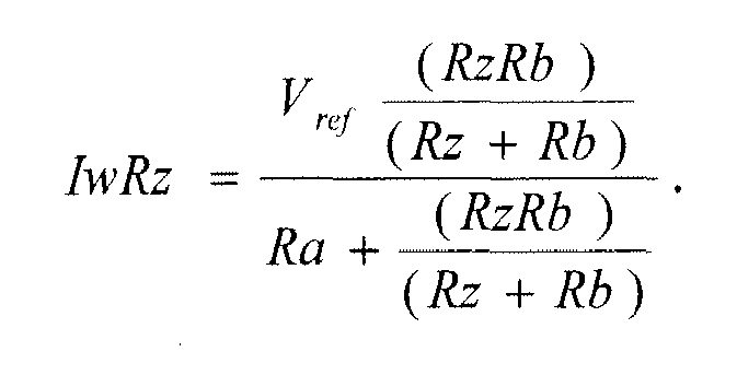


processor 126 implements to determine the wiper resistance (Rw) of thepotentiometer 102. - While the invention has been described with reference to a preferred embodiment, it will be understood by those skilled in the art that various changes may be made and equivalents may be substituted for elements thereof without departing from the scope of the invention. In addition, many modifications may be made to adapt to a particular situation or material to the teachings of the invention without departing from the essential scope thereof. Therefore, it is intended that the invention not be limited to the particular embodiment disclosed as the best mode contemplated for carrying out this invention, but that the invention will include all embodiments falling within the scope of the appended claims.
Claims (10)
- A method of determining wiper resistance of a potentiometer (102) including a first terminal (108-1), a second terminal (108-2), a third terminal (108-3), a resistive element (110) having a potentiometer resistance electrically coupled between the first and second terminals (108-1, 108-2), and a wiper (112) electrically coupled between the resistive element and the third terminal (108-3) and movable to a wiper position between the first and second terminals (108-1, 108-2), the method comprising the steps of:electrically energizing the potentiometer (102);electrically coupling a sense resistor (104) to the potentiometer third terminal (108-3), the sense resistor (104) having a substantially constant sense resistance;determining a potentiometer voltage, the potentiometer voltage being a voltage potential between the potentiometer first and second terminals (108-1, 108-2);determining the wiper position based at least in part on the determined potentiometer voltage;electrically coupling the sense resistor (104) to a potential that causes a wiper current to flow through the wiper (112) and sense resistor (104);determining a magnitude of the wiper current; anddetermining the wiper resistance based at least in part on the potentiometer resistance, the determined potentiometer position, the determined wiper current magnitude, and the sense resistance.
- The method of Claim 1, wherein the step of determining the wiper position comprises:substantially preventing current flow through the sense resistor (104);determining a no-load wiper voltage at the potentiometer third terminal (108-3); andcalculating the wiper position by dividing the determined no-load wiper voltage by the determined potentiometer voltage.
- The method of Claim 1, wherein the step of determining the magnitude of the wiper current comprises:determining a wiper voltage at the potentiometer third terminal (108-3) when the wiper current flows through the wiper (112) and sense resistor (104); andcalculating the wiper current magnitude from the determined wiper voltage and the sense resistance.
- The method of Claim 1, wherein the potentiometer resistance includes a first resistance between the first terminal (108-1) and the wiper (112), and a second resistance between the second terminal (108-2) and the wiper (112), and wherein the method further comprises:determining the second resistance from the potentiometer resistance and the determined wiper position; anddetermining the first resistance from the potentiometer resistance and the determined second resistance.
- The method of Claim 4, wherein the wiper resistance is determined from the potentiometer resistance, the determined first resistance, the determined second resistance, the determined wiper current magnitude, and the sense resistance.
- A potentiometer wiper resistance measurement circuit, comprising:a potentiometer (102) including a first terminal (108-1), a second terminal (108-2), a third terminal (108-3), a resistive element (110) having a potentiometer resistance electrically coupled between the first and second terminals (108-1, 108-2), and a wiper (112) electrically coupled between the resistive element and the third terminal (108-3) and movable to a wiper position between the first and second terminals (108-1, 108-2);a sense resistor (104) having a substantially constant sense resistance and including a first terminal (118-1) and a second terminal (118-2), the sense resistor first terminal (118-1) coupled to the potentiometer third terminal (108-3);a power source electrically coupled to the potentiometer and configured to supply a current thereto that results in a voltage drop between the potentiometer first and second terminals (108-1, 108-2); andan output circuit (106) having a plurality of input terminals (122) and an output terminal (124), separate ones of the output circuit input terminals coupled to at least the potentiometer first terminal (108-1), the potentiometer second terminal (108-2), and the sense resistor second terminal, the output circuit operable to selectively couple (i) the potentiometer first terminal (108-1) to the output terminal, (ii) the potentiometer third terminal (108-3) to the output terminal, and (iii) the sense resistor second terminal (108-2) to a reference potential.
- The circuit of Claim 6, wherein the output circuit (106) includes:a first multiplexer (128) having a plurality of input terminals (146) and an output terminal (148), a first of the input terminals coupled to the potentiometer first terminal (108-1), a second of the input terminals coupled to the potentiometer third terminal (108-3);a second multiplexer (132) having a plurality of input terminals (146) and an output terminal (148), a first of the input terminals coupled to the sense resistor second terminal (118-2);a third multiplexer (134) having a plurality of input terminals (146) and an output terminal (148), a first of the input terminals coupled to the reference potential, the output terminal coupled to the second multiplexer output terminal; anda fourth multiplexer (136) having a plurality of input terminals (146) and an output terminal (148), a first of the input terminals coupled to the first multiplexer output terminal , a second of the input terminals coupled to the second multiplexer output terminal.
- The circuit of Claim 7, wherein:the first of the third multiplexer input terminals is further coupled to the potentiometer second terminal (108-2); anda second of the third multiplexer input terminals is coupled to the potentiometer second terminal (108-2).
- The circuit of Claim 7, further comprising:an analog-to-digital converter (ADC) (138) coupled to the fourth multiplexer output terminal (142); andan amplifier coupled between the ADC and the fourth multiplexer output terminal.
- The circuit of Claim 6, further comprising:a processor (126) coupled to receive signals supplied from the output circuit output terminal (124) and selectively operable, upon receipt thereof, to determine the potentiometer wiper resistance.
Applications Claiming Priority (1)
| Application Number | Priority Date | Filing Date | Title |
|---|---|---|---|
| US11/502,956 US7550981B2 (en) | 2006-08-10 | 2006-08-10 | Circuit and method for determining potentiometer wiper resistance |
Publications (1)
| Publication Number | Publication Date |
|---|---|
| EP1887368A1 true EP1887368A1 (en) | 2008-02-13 |
Family
ID=38672065
Family Applications (1)
| Application Number | Title | Priority Date | Filing Date |
|---|---|---|---|
| EP07113842A Withdrawn EP1887368A1 (en) | 2006-08-10 | 2007-08-06 | Circuit and method for determining potentionmeter wiper resistance |
Country Status (2)
| Country | Link |
|---|---|
| US (1) | US7550981B2 (en) |
| EP (1) | EP1887368A1 (en) |
Cited By (2)
| Publication number | Priority date | Publication date | Assignee | Title |
|---|---|---|---|---|
| EP2602695A1 (en) * | 2011-12-09 | 2013-06-12 | Thales | Data input device with potentiometer and control stick for piloting an aircraft, the control stick including the data input device |
| FR3129768A1 (en) * | 2021-12-01 | 2023-06-02 | Crouzet | Button |
Families Citing this family (2)
| Publication number | Priority date | Publication date | Assignee | Title |
|---|---|---|---|---|
| DE102007009573A1 (en) * | 2007-02-27 | 2008-09-04 | Up Management Gmbh & Co Med-Systems Kg | One-way sensor unit for patient observation, and arterial blood pressure sensor unit, has sensor provided around electrical quantity, which is based on quantity that has to be determined, and signal terminal that is provided around outlet |
| US9281833B2 (en) * | 2012-05-28 | 2016-03-08 | Avago Technologies General Ip (Singapore) Pte. Ltd. | Analog-to-digital converter with power supply-based reference |
Citations (6)
| Publication number | Priority date | Publication date | Assignee | Title |
|---|---|---|---|---|
| DE3522775A1 (en) * | 1985-06-26 | 1987-01-08 | Daimler Benz Ag | Device for determining the contact resistance on the slider of a potentiometer |
| EP0354269A1 (en) | 1988-08-09 | 1990-02-14 | VDO Adolf Schindling AG | Circuitry for monotoring the contact resistance of a potentiometer |
| DE4443941A1 (en) * | 1994-12-09 | 1996-06-27 | Knorr Bremse Systeme | Quasi-real=time testing of sensor and wiring to measuring appts. |
| FR2735871A1 (en) * | 1995-06-23 | 1996-12-27 | Renault | Diagnostic method for detecting connection and wiring faults in automobile potentiometers |
| EP0759558A2 (en) | 1995-08-18 | 1997-02-26 | Siemens Aktiengesellschaft | Testing method for an analog input channel of an analog signal detecting circuit and the corresponding analog signal detecting circuit |
| EP1022570A2 (en) | 1999-01-22 | 2000-07-26 | Honeywell Inc. | Failsafe monitoring system for potentiometers |
Family Cites Families (14)
| Publication number | Priority date | Publication date | Assignee | Title |
|---|---|---|---|---|
| US2912165A (en) * | 1955-05-06 | 1959-11-10 | Schlumberger Well Surv Corp | Computer |
| US3852665A (en) | 1972-02-17 | 1974-12-03 | Bunker Ramo | Apparatus for testing potentiometers |
| US3810008A (en) | 1973-08-16 | 1974-05-07 | Motoda Electronics | Apparatuses for detecting failure in a potentiometer circuit |
| US4218745A (en) | 1978-09-11 | 1980-08-19 | Lockheed Corporation | Microcomputer assisted electrical harness fabrication and testing system |
| DE3621937A1 (en) | 1986-06-30 | 1988-01-07 | Bosch Gmbh Robert | MONITORING DEVICE FOR AN ELECTRONIC CONTROL DEVICE IN A MOTOR VEHICLE |
| US4866363A (en) | 1987-09-21 | 1989-09-12 | Honeywell Inc. | Fail-safe potentiometer feedback system |
| US4987372A (en) | 1989-08-01 | 1991-01-22 | Lutron Electronics Co., Inc. | Potentiometer state sensing circuit |
| DE4116603A1 (en) | 1991-05-22 | 1992-11-26 | Vdo Schindling | CIRCUIT ARRANGEMENT FOR MONITORING THE CONTACT BETWEEN THE RESISTANCE TRACK AND THE GRINDER OF A POTENTIOMETER |
| US5241277A (en) | 1992-02-28 | 1993-08-31 | United Technologies Corporation | Test system for automatic testing of insulation resistance, capacitance and attenuation of each contact pair in a filter pin connector |
| US5542279A (en) * | 1994-09-30 | 1996-08-06 | Honeywell Inc. | Method of incorporating wide tolerance set point potentiometers into devices with fixed orientation setpoint indicator scales |
| US5812411A (en) | 1995-07-14 | 1998-09-22 | Calabrese; Joseph S. | Tapped variable potentiometer resistor with current sense and safety circuit |
| DE19751556C1 (en) | 1997-11-20 | 1999-06-10 | Delphi Automotive Systems Gmbh | Diagnostic circuit for potentiometric sensors |
| US6075370A (en) | 1998-03-27 | 2000-06-13 | Aladdin Enterprises, Inc. | Method of calibrating a potentiometer |
| EP1447670A1 (en) | 2003-02-12 | 2004-08-18 | Dialog Semiconductor GmbH | Sensor read out |
-
2006
- 2006-08-10 US US11/502,956 patent/US7550981B2/en not_active Expired - Fee Related
-
2007
- 2007-08-06 EP EP07113842A patent/EP1887368A1/en not_active Withdrawn
Patent Citations (6)
| Publication number | Priority date | Publication date | Assignee | Title |
|---|---|---|---|---|
| DE3522775A1 (en) * | 1985-06-26 | 1987-01-08 | Daimler Benz Ag | Device for determining the contact resistance on the slider of a potentiometer |
| EP0354269A1 (en) | 1988-08-09 | 1990-02-14 | VDO Adolf Schindling AG | Circuitry for monotoring the contact resistance of a potentiometer |
| DE4443941A1 (en) * | 1994-12-09 | 1996-06-27 | Knorr Bremse Systeme | Quasi-real=time testing of sensor and wiring to measuring appts. |
| FR2735871A1 (en) * | 1995-06-23 | 1996-12-27 | Renault | Diagnostic method for detecting connection and wiring faults in automobile potentiometers |
| EP0759558A2 (en) | 1995-08-18 | 1997-02-26 | Siemens Aktiengesellschaft | Testing method for an analog input channel of an analog signal detecting circuit and the corresponding analog signal detecting circuit |
| EP1022570A2 (en) | 1999-01-22 | 2000-07-26 | Honeywell Inc. | Failsafe monitoring system for potentiometers |
Cited By (5)
| Publication number | Priority date | Publication date | Assignee | Title |
|---|---|---|---|---|
| EP2602695A1 (en) * | 2011-12-09 | 2013-06-12 | Thales | Data input device with potentiometer and control stick for piloting an aircraft, the control stick including the data input device |
| FR2983987A1 (en) * | 2011-12-09 | 2013-06-14 | Thales Sa | POTENTIOMETER DATA ENTRY DEVICE AND HANDLE FOR DRIVING AN AIRCRAFT, THE HAND COMPRISING THE DATA ENTRY DEVICE |
| US9188614B2 (en) | 2011-12-09 | 2015-11-17 | Thales | Data input device with a potentiometer, and joystick intended for piloting an aircraft, said joystick comprising the data input device |
| FR3129768A1 (en) * | 2021-12-01 | 2023-06-02 | Crouzet | Button |
| WO2023099490A1 (en) | 2021-12-01 | 2023-06-08 | Crouzet | Button |
Also Published As
| Publication number | Publication date |
|---|---|
| US20080100303A1 (en) | 2008-05-01 |
| US7550981B2 (en) | 2009-06-23 |
Similar Documents
| Publication | Publication Date | Title |
|---|---|---|
| US6853306B1 (en) | Circuit arrangement for measuring the resistance of resistors in a pressure-sensitive resistor mat | |
| US7683604B1 (en) | Amplifier topology and method for connecting to printed circuit board traces used as shunt resistors | |
| CN109791178B (en) | Apparatus and method for smart sensor applications | |
| CN109946510B (en) | Method and battery sensor for identifying load current | |
| CN112834974B (en) | Method for testing battery sensor, and battery sensor | |
| EP1922554B1 (en) | Current measurement circuit and method of diagnosing faults in same | |
| CN107229028A (en) | Method and battery sensor for determining load current | |
| CN114076843B (en) | Current sensor element, current sensor unit and method of measuring current | |
| JP3309380B2 (en) | Digital measuring instrument | |
| US11280819B2 (en) | Circuit arrangement and method for determining a resistance change and methods for determining lead resistances | |
| US7550981B2 (en) | Circuit and method for determining potentiometer wiper resistance | |
| US8872530B2 (en) | Method for correcting the voltage measured across the terminals of a sensor | |
| JPH05129093A (en) | Triple probe plasma measuring instrument for correcting space electric potential error | |
| JP3393203B2 (en) | Inspection method of current detection circuit | |
| JP4209429B2 (en) | Strain / temperature measurement method | |
| CN112714873A (en) | Battery sensor for measuring current independently of temperature using a shunt | |
| JP2008215844A (en) | Current detection device | |
| JPH11281677A (en) | Current measuring apparatus | |
| CN111044910A (en) | Method for operating a battery sensor and battery sensor | |
| JP2006349686A (en) | Improved bridge apparatus for correcting electrical signal | |
| US20180275701A1 (en) | Voltage supply apparatus | |
| JPS6314784B2 (en) | ||
| US11959957B2 (en) | Measuring device for a motor vehicle | |
| JPH04315062A (en) | Method for measuring resistance value of resistor | |
| US6290828B1 (en) | Circuit for measuring oxygen concentration |
Legal Events
| Date | Code | Title | Description |
|---|---|---|---|
| PUAI | Public reference made under article 153(3) epc to a published international application that has entered the european phase |
Free format text: ORIGINAL CODE: 0009012 |
|
| AK | Designated contracting states |
Kind code of ref document: A1 Designated state(s): AT BE BG CH CY CZ DE DK EE ES FI FR GB GR HU IE IS IT LI LT LU LV MC MT NL PL PT RO SE SI SK TR |
|
| AX | Request for extension of the european patent |
Extension state: AL BA HR MK YU |
|
| 17P | Request for examination filed |
Effective date: 20080731 |
|
| 17Q | First examination report despatched |
Effective date: 20080826 |
|
| AKX | Designation fees paid |
Designated state(s): DE FR GB |
|
| STAA | Information on the status of an ep patent application or granted ep patent |
Free format text: STATUS: THE APPLICATION IS DEEMED TO BE WITHDRAWN |
|
| 18D | Application deemed to be withdrawn |
Effective date: 20110301 |