EP1887339A1 - Method, device and system for evaluating a lens for an electronic device - Google Patents
Method, device and system for evaluating a lens for an electronic device Download PDFInfo
- Publication number
- EP1887339A1 EP1887339A1 EP06016650A EP06016650A EP1887339A1 EP 1887339 A1 EP1887339 A1 EP 1887339A1 EP 06016650 A EP06016650 A EP 06016650A EP 06016650 A EP06016650 A EP 06016650A EP 1887339 A1 EP1887339 A1 EP 1887339A1
- Authority
- EP
- European Patent Office
- Prior art keywords
- lens
- approximately
- pattern
- evaluation
- lines
- Prior art date
- Legal status (The legal status is an assumption and is not a legal conclusion. Google has not performed a legal analysis and makes no representation as to the accuracy of the status listed.)
- Granted
Links
Images



Classifications
-
- G—PHYSICS
- G01—MEASURING; TESTING
- G01M—TESTING STATIC OR DYNAMIC BALANCE OF MACHINES OR STRUCTURES; TESTING OF STRUCTURES OR APPARATUS, NOT OTHERWISE PROVIDED FOR
- G01M11/00—Testing of optical apparatus; Testing structures by optical methods not otherwise provided for
- G01M11/02—Testing optical properties
- G01M11/0242—Testing optical properties by measuring geometrical properties or aberrations
-
- G—PHYSICS
- G01—MEASURING; TESTING
- G01M—TESTING STATIC OR DYNAMIC BALANCE OF MACHINES OR STRUCTURES; TESTING OF STRUCTURES OR APPARATUS, NOT OTHERWISE PROVIDED FOR
- G01M11/00—Testing of optical apparatus; Testing structures by optical methods not otherwise provided for
- G01M11/02—Testing optical properties
- G01M11/0242—Testing optical properties by measuring geometrical properties or aberrations
- G01M11/0257—Testing optical properties by measuring geometrical properties or aberrations by analyzing the image formed by the object to be tested
- G01M11/0264—Testing optical properties by measuring geometrical properties or aberrations by analyzing the image formed by the object to be tested by using targets or reference patterns
-
- G—PHYSICS
- G01—MEASURING; TESTING
- G01M—TESTING STATIC OR DYNAMIC BALANCE OF MACHINES OR STRUCTURES; TESTING OF STRUCTURES OR APPARATUS, NOT OTHERWISE PROVIDED FOR
- G01M11/00—Testing of optical apparatus; Testing structures by optical methods not otherwise provided for
- G01M11/02—Testing optical properties
- G01M11/0242—Testing optical properties by measuring geometrical properties or aberrations
- G01M11/0278—Detecting defects of the object to be tested, e.g. scratches or dust
-
- G—PHYSICS
- G02—OPTICS
- G02F—OPTICAL DEVICES OR ARRANGEMENTS FOR THE CONTROL OF LIGHT BY MODIFICATION OF THE OPTICAL PROPERTIES OF THE MEDIA OF THE ELEMENTS INVOLVED THEREIN; NON-LINEAR OPTICS; FREQUENCY-CHANGING OF LIGHT; OPTICAL LOGIC ELEMENTS; OPTICAL ANALOGUE/DIGITAL CONVERTERS
- G02F1/00—Devices or arrangements for the control of the intensity, colour, phase, polarisation or direction of light arriving from an independent light source, e.g. switching, gating or modulating; Non-linear optics
- G02F1/01—Devices or arrangements for the control of the intensity, colour, phase, polarisation or direction of light arriving from an independent light source, e.g. switching, gating or modulating; Non-linear optics for the control of the intensity, phase, polarisation or colour
- G02F1/13—Devices or arrangements for the control of the intensity, colour, phase, polarisation or direction of light arriving from an independent light source, e.g. switching, gating or modulating; Non-linear optics for the control of the intensity, phase, polarisation or colour based on liquid crystals, e.g. single liquid crystal display cells
- G02F1/133—Constructional arrangements; Operation of liquid crystal cells; Circuit arrangements
- G02F1/1333—Constructional arrangements; Manufacturing methods
- G02F1/1335—Structural association of cells with optical devices, e.g. polarisers or reflectors
- G02F1/133526—Lenses, e.g. microlenses or Fresnel lenses
Definitions
- the invention generally relates to a method, device and system for evaluating a lens for a display in an electronic device, in particular a display lens of a communication device, such as a portable phone.
- a typical voice communication device such as a cellular phone, has a display therein, which is frequently a liquid crystal display (LCD).
- LCD liquid crystal display
- an LCD is comprised of a liquid crystal substance sandwiched between an upper and lower plate of generally thin glass.
- the layout of a display in a communication device frequently has a lens provided over the LCD.
- the lens provides a physical cover for the-upper plate of glass of the top of the LCD itself.
- the lens can be thicker than LCD's glass top, thereby providing protection from when external downward pressure applied to the upper surface of the LCD.
- the lens introduces additional visual interface between the LCD and the viewer. This can lead to distortions to the LCD if there are optic defects in the lens. As the lens is typically clear, it is difficult to determine when a lens is defective, until it is installed into a device and the LCD is activated. This is inefficient for the manufacturing process.
- Fig. 1 is a top plan view of a communication device having a liquid crystal display (LCD) and a lens that may be evaluated according to embodiment of the invention;
- LCD liquid crystal display
- Fig. 2 is a top exploded perspective view of selected internal components including the LCD display and the lens of the communication device of Fig. 1;
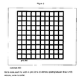
- Fig. 3 is a schematic diagram of an evaluation grid used to evaluate the lens of the device of Fig. 1 according to an embodiment
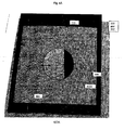
- Fig. 4A is a schematic of an exemplary distortion pattern seen through a lens having a defect when the grid of Fig. 3 is placed underneath;
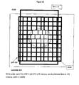
- Fig. 4B is another schematic of an exemplary distortion pattern seen through a lens having a defect when the grid of Fig. 3 is placed underneath;
- Fig. 5 is a block diagram of an evaluation system utilizing the grid of Fig. 3 for evaluating a lens of the device of Fig. 1 according to an embodiment.
- an evaluation device for visually identifying imperfections in a lens for a display for an electronic device is preferably provided.
- the evaluation device may comprise: a substrate; and a pattern imposed on the substrate.
- the pattern when the pattern is viewed through the lens, the pattern is distorted around an area where a defect is present in the lens-
- the device assists in visually identifying imperfections in the lens when the substrate is positioned relative to the lens to enable the pattern to be viewed through the lens.
- the substrate may be comprised of a transparent material and the pattern may be a series of lines shown in a dark colour.
- the series of lines may be a grid having lines approximately 50 microns thick, spaced in approximately 100 micron intervals from center to center.
- the grid may have lines having thickness of between approximately 10 to approximately 150 microns, spaced in intervals between approximately 20 microns to approximately 300 microns from center to center.
- the substrate may be comprised of an opaque material in a light colour; and the pattern may be a series of Lines shown in a dark colour.
- the series of lines may be a grid having lines approximately 50 microns thick, spaced in approximately 100 micron intervals from center to center.
- the grid may have lines having thickness of between approximately 10 to approximately 150 microns, spaced in intervals between approximately 20 microns to approximately 300 microns from center to center.
- the pattern may be a series of geometric shapes, each having dimensions of between approximately 10 to approximately 150 microns.
- a system to evaluate a lens for a display for an electronic device for imperfections comprises: an evaluation table for the lens, the table having a mounting area; and a substrate for mounting on the mounting area, the substrate having a pattern imposed thereon wherein when the pattern is viewed through the lens, the pattern is noticeably distorted around an area where a defect is present in the lens.
- the system may further comprise: a light mounted within the table to provide backlighting for the substrate; and a guide rail system for the lens to place the lens above the mounting area.
- the system may further comprise a conveyor for the lens to selectively transport the lens to and from the mounting area.
- the substrate may be comprised of a transparent material; and the pattern may be a grid shown in a dark colour. Further, the grid may have lines having thickness of between approximately 10 to approximately 150 microns spaced in intervals between approximately 20 microns to approximately 300 microns from center to center.
- a method for evaluating a lens for a display for an electronic device for imperfections comprises: placing the lens under evaluation over an evaluation substrate having an evaluation pattern; examining an image of the test pattern appearing through the lens for a distortion in the pattern; and identifying the lens as defective is the distortion is found.
- the pattern comprises a series of lines having a thickness of approximately 50 microns.
- the series of lines may be a grid having lines having thickness of between approximately 10 to approximately 150 microns and the lines may be spaced between approximately 20 to approximately 150 microns apart.
- an embodiment provides a system, method and device for evaluating a lens prior to installing the lens in an electronic device.
- a substrate is provided having a finely impressed pattern provided thereon.
- the pattern viewed through the lens can be viewed for any distortions in its image. If a significant or noticeable distortion is viewed and visually identified, then a distortion is present in the lens and it should be rejected and should not be installed into a device.
- Various patterns and substrates can be provided.
- communication device 100 provides voice communications with other devices, allowing the user to hear audio signals (e.g, voices) transmitted from another device (e.g. a cellular phone).
- Device 100 may be a telephone, a cordless telephone, a cellular telephone, a voice-enabled personal digital assistant (PDA) or any other voice communication device. Communications may be provided via wireless systems, wired systems or a combination of both systems.
- PDA personal digital assistant
- device 100 has a keypad 102, display 104, microphone 106 and transducer 108, i.e. speaker 108, all contained within an enclosure.
- Display 104 is an LCD device.
- Display lens 110 provides a transparent, translucent or non-opaque physical cover for the viewing area of display 104 and extends beyond it.
- Speaker cover 112 covers a recess in display lens 110. The recess is located above the installation location of speaker 108.
- Case 114 provides a physical enclosure for the electronics and mechanical elements for device 100. General internal circuits and operations of device 100 are well known in the art and are not provided here.
- Device 100 provides voice communications for a user in a familiar compact form factor. To initiate a call, the user activates device 100, enters a telephone number to be called on keypad 102 and initiates the call.
- view 200 provides an exploded top perspective view of internal and external elements in an upper portion of device 100.
- case 114 is comprised of top case section 202 and a bottom case section (not shown).
- Top case section 202 provides a one-piece cover for internal elements of device 100.
- Top case section 202 mates with the bottom case section along their respective sides.
- Various dimensions and fitting interfaces between top case section 202 and bottom case section may be provided in other embodiments, including those known in the art.
- top case section 202 is shaped to define the front face of device 100 and the top portion of the exterior edge of case 114, Top section 202 also provides internal bracing for structural support for device 100 and has two openings in its front face: opening 204 allows access to keypad 102 and opening 206 allows viewing of LCD 104. Top case section 202 is preferably a plastic moulded injected casing.
- Display area of LCD 104 is covered by display lens 110.
- Display lens 110 further extends upwardly above LCD 104 to the top edge of case section 202.
- display lens 110 provides a single seamless structure to cover both LCD 104 and speaker 108.
- display lens 110 may be silk screened with custom lettering or graphics around display area of LCD 104 and around the area where speaker 108 is located.
- Display lens 110 may be made of almost any material (such as plastic), as long as the material facilitates accurate manufacturing of display lens 110 and provides a transparent, translucent or non-opaque region where display 104 will be placed underneath. Other sizes, shapes and thicknesses of lens 110 can be provided to fit dimensions of a particular display 104.
- recess 208 is provided, which is a shaped contour extending inwardly within display lens 110.
- recess 208 is a hexagonal polygon depression having a generally stunted-hexagonal shape.
- the floor of recess 208 is generally flat.
- the exterior edges of recess 208 are bevelled downward to the floor.
- other shapes may be provided for a recess.
- Recess 208 has four sound holes 210 therein which provide air conduits through display lens 110. As such, holes 210 allow passage of acoustic energy from speaker 108 through display lens 110 to the ambient environment outside device 100.
- Speaker cover 112 is shaped to fit within recess 208. As such in the embodiment, cover 112 is a stunted hexagonal shape. Speaker cover 112 provides a cover for sound holes 210, thereby enhancing the aesthetic appearance of display lens 110.
- adhesive display cover tape 212 is provided and is located between LCD 104 and display lens 110.
- Display cover tape 212 has double-sided adhesive thereon to affix its top surface to the bottom surface of display lens 110 and to affix its bottom surface to the top surface of case section 202.
- Display cover tape 212 is excised in area 214 so as to not obstruct view of LCD 104.
- cover tape 212 is black, which enhances concealing of plastics elements beneath it and outlining of the display area of LCD 104.
- Display cover tape 212 has a transparent layer attached in area 214. After attaching tape 212 to display lens 110, the transparent layer is removed using a pull tab.
- the display cover can be any shape and size, as long as it covers both the display region and the speaker of the communication device. Further, if the display and the speaker are not on the same face of a device, the display cover can be shaped to bend at the interface line between the two faces and cover both the display and the speaker.
- lens 110 provides a thicker transparent or tinted window covering LCD 104.
- One type of lens 110 provides no visual magnification of LCD 104.
- a lens may be formed to provide magnification over one or more regions of LCD 104.
- Lens 110 may be manufactured from a clear polycarbonate, such as Lexan (trademark).
- Lexan trademark
- lens 110 In order to limit distortions of images as light passes from LCD 14 through lens 110 to the viewer, it is preferable that lens 110 have minimal distortions therein. However, it is inevitable that during the manufacturing or shipping of lens 110, some imperfections may be imparted onto lens 110, that will impair the clarity of lens 110.
- Such imperfections may not be readily visible to the unaided eye, but would be apparent once the cover is installed in situ in device 10 and when LCD 104 is generating an image. For example, a straight line generated on LCD 104 may appear bent in some regions once distorted by a defective lens 110. Alternatively or moiré effects.
- an embodiment provides a pattern 302 that is printed, etched, embossed or otherwise painted on a substrate 300 that is used to highlight an imperfection in lens 110 that would normally not be visible unless lens 110 was installed into device 10.
- the colour of the lines is black, however, in other embodiments, any sufficiently dark colour may be used, such as green, blue, brown or others.
- Substrate 300 is a clear mylar sheet; however, it can also be a bright white substrate or a rigid piece of glass or clear or bright plastic.
- a feature of pattern 302 as provided on the substrate is that it is visible from the background provided by the substrate.
- a grid may be generated using a high definition laser plotter, such as one meant for halide based film. Any suitable photolithographic high resolution process would be a possible alternative.
- pattern 302 is a cross hatching grid of evenly spaced lines in evenly spaced rows and columns.
- the widths of each line is approximately 50 microns.
- the spacing between each line in each row and column is approximately 100 microns, center to center.
- the size of the grid can vary, depending on the size of lens 110 being evaluated.
- An exemplary grid has exterior dimensions of 9 cm x 14 cm centered on a clear mylar sheet 10 cm x 16 cm in size.
- the widths may change and or the spacings may change for the lines throughout the pattern.
- the pattern may or may not have a symmetrical aspect to it.
- grid 302 Other configurations for grid 302 may be used. For example, line widths of 25 microns may be used in 25 micron spacings between exterior sides of the lines (this provides a "center-to-center” spacing of 50 microns). Similarly, line widths of 75,100, 125, 150 microns may be used ( or approximations thereof with larger or smaller dimensions allowable). For such widths, the "center to center" spacing between lines may be approximately double the thickness of the lines. This spacing provides a uniform alternation between lines and "white” spaces. The lines may be spaced in larger or smaller dimensions than their thickness. In one embodiment, all lines in grid 302 are of the same thickness and have the same spacing.
- grid 302 may have one or more regions having different thicknesses and / or spacings of lines from other regions.
- alternative patterns may be provided, including a pattern is a series of evenly spaced dots, forming a Benday dot arrangement, or a series of geometric shapes, such as squares, rectangles, triangles, rhombuses, circles etc. Exemplary dimensions of such geometric shapes, would be having sides in the range of 10 microns to 150 microns. Spacing of shapes would be in a similar range of dimensions.
- a method for testing a lens as provided by an embodiment is as follows. First, substrate 300 is placed on a flat surface in a well-lit environment. Next, lens 110 is placed on top or is held slightly above substrate 300. An assessor evaluates the image of grid 302 appearing through lens 110 to evaluate the optical quality of lens 110. For an acceptable lens 110, when lens 110 is placed on top of the substrate 300 and the image of grid 302 is viewed therethrough, the image has no or only marginal distortions of the grid pattern 302. However, for a lens 110 that has an optic imperfection in an area, the imperfection is manifested by a distortion in the grey scale image of grid 302 seen through that area.
- An imperfection may be caused by almost any manufacturing / composition error, including a bulging of a thickness dimension in lens 110, an air bubble in lens 110, a foreign particular / substance trapped within lens 110, etc.
- An imperfection may produce almost any type of visible distortion in the grid image seen through lens 110.
- One type of distortion is that the grid pattern appears to change in the change of the colour from a constant (grey) hue to a moiré pattern.
- Fig 4A shows layout 400A having substrate 300 with grid 302 on a flat surface with lens 110 placed upon substrate 300.
- exemplary hairline line 404 is indicative one type of defect as magnified in balloon 406, which is provided for magnification purposes for the figure.
- 4B in view 400B shows another exemplary visualization of a defect of an exemplary bulging of image of grid 302 when viewed through a defective lens 110 in defective region 402B (circled for illustrative purposes). If a notable imperfection is found in the image, then the lens is rejected. If no significant imperfection is found, the lens may be accepted and eventually installed into a device. It will be appreciated that other manifestations of defects may be provided when viewing a lens.
- lens 110 may be held above substrate 300 as well. If substrate 300 is transparent, then backlighting may be used, such as lighting from a light table. If substrate 300 is opaque, then ambient lighting from above lens 110 can be used.
- an automated jig and evaluation station 500 may be implemented where a light table 502 has grid 302 mounted on its upper surface.
- An evaluation method as described above may be used with station 500.
- a bin 504 of lenses 110 to be tested is provided and the evaluator can individually take a lens 110 from bin 504 and align it on table 502 over a mounting area using guide rails 506 then examine the lens under test 110A over grid 302. If the lens under test 110A does not show at least one significant distortion, change in light intensity or variability in contrast in the image of grid 302, it is considered to be a passed lens and is placed in pass bin 508 for eventual installation into a device.
- the lens under test 110A shows at least one significant distortion, change in light intensity or variability in contrast in the image of grid 302, it is considered to be a failed lens and is placed in fail bin 510.
- Such lens would typically not be installed into a device and may be returned to the supplier.
- an automated displacer and conveyor system may be provided to selectively automatically take a lens from bin 504 then convey it over grid 302 for evaluation then selectively place the lens under test in either bin 508 or 510 depending on the decision of the evaluator.
- Backlight 512 may be provided in table 502 to illuminate the mounting area and grid 302.
- an automated computer vision system may also be provided to scan the pattern "seen" through lens 110 and assess whether the image seen through lens 110 is acceptable or not.
Landscapes
- Physics & Mathematics (AREA)
- Chemical & Material Sciences (AREA)
- General Physics & Mathematics (AREA)
- Geometry (AREA)
- Analytical Chemistry (AREA)
- Nonlinear Science (AREA)
- Mathematical Physics (AREA)
- Crystallography & Structural Chemistry (AREA)
- Optics & Photonics (AREA)
- Testing Of Optical Devices Or Fibers (AREA)
- Devices For Indicating Variable Information By Combining Individual Elements (AREA)
- Investigating Materials By The Use Of Optical Means Adapted For Particular Applications (AREA)
Abstract
Description
- The invention generally relates to a method, device and system for evaluating a lens for a display in an electronic device, in particular a display lens of a communication device, such as a portable phone.
- A typical voice communication device, such as a cellular phone, has a display therein, which is frequently a liquid crystal display (LCD). As is known in the art, an LCD is comprised of a liquid crystal substance sandwiched between an upper and lower plate of generally thin glass.
- The layout of a display in a communication device frequently has a lens provided over the LCD. The lens provides a physical cover for the-upper plate of glass of the top of the LCD itself. The lens can be thicker than LCD's glass top, thereby providing protection from when external downward pressure applied to the upper surface of the LCD.
- However, the lens introduces additional visual interface between the LCD and the viewer. This can lead to distortions to the LCD if there are optic defects in the lens. As the lens is typically clear, it is difficult to determine when a lens is defective, until it is installed into a device and the LCD is activated. This is inefficient for the manufacturing process.
- There is a need for a system and method to evaluate such lenses prior to installation to a device which provides an improvement over the prior art and the viewer.
- The foregoing and other aspects of the invention will become more apparent from the following description of specific embodiments thereof and the accompanying drawings which illustrate, by way of example only, the principles of the invention. In the drawings, where like elements feature like reference numerals (and wherein individual elements bear unique alphabetical suffixes):
- Fig. 1 is a top plan view of a communication device having a liquid crystal display (LCD) and a lens that may be evaluated according to embodiment of the invention;
- Fig. 2 is a top exploded perspective view of selected internal components including the LCD display and the lens of the communication device of Fig. 1;
- Fig. 3 is a schematic diagram of an evaluation grid used to evaluate the lens of the device of Fig. 1 according to an embodiment;
- Fig. 4A is a schematic of an exemplary distortion pattern seen through a lens having a defect when the grid of Fig. 3 is placed underneath;
- Fig. 4B is another schematic of an exemplary distortion pattern seen through a lens having a defect when the grid of Fig. 3 is placed underneath; and
- Fig. 5 is a block diagram of an evaluation system utilizing the grid of Fig. 3 for evaluating a lens of the device of Fig. 1 according to an embodiment.
- The description which follows, and the embodiments described therein, are provided by way of illustration of an example, or examples, of particular embodiments of the principles of the present invention. These examples are provided for the purposes of explanation, and not limitation, of those principles and of the invention. In the description, which follows, like parts are marked throughout the specification and the drawings with the same respective reference numerals.
- In a first aspect of an embodiment, an evaluation device for visually identifying imperfections in a lens for a display for an electronic device is preferably provided. The evaluation device may comprise: a substrate; and a pattern imposed on the substrate. For the pattern, when the pattern is viewed through the lens, the pattern is distorted around an area where a defect is present in the lens- As such, the device assists in visually identifying imperfections in the lens when the substrate is positioned relative to the lens to enable the pattern to be viewed through the lens.
- In the device, the substrate may be comprised of a transparent material and the pattern may be a series of lines shown in a dark colour. Further, the series of lines may be a grid having lines approximately 50 microns thick, spaced in approximately 100 micron intervals from center to center. Alternatively, the grid may have lines having thickness of between approximately 10 to approximately 150 microns, spaced in intervals between approximately 20 microns to approximately 300 microns from center to center.
- Alternatively, the substrate may be comprised of an opaque material in a light colour; and the pattern may be a series of Lines shown in a dark colour. Further, the series of lines may be a grid having lines approximately 50 microns thick, spaced in approximately 100 micron intervals from center to center. Alternatively, the grid may have lines having thickness of between approximately 10 to approximately 150 microns, spaced in intervals between approximately 20 microns to approximately 300 microns from center to center.
- The pattern may be a series of geometric shapes, each having dimensions of between approximately 10 to approximately 150 microns.
- In a second aspect, a system to evaluate a lens for a display for an electronic device for imperfections is provided. The system comprises: an evaluation table for the lens, the table having a mounting area; and a substrate for mounting on the mounting area, the substrate having a pattern imposed thereon wherein when the pattern is viewed through the lens, the pattern is noticeably distorted around an area where a defect is present in the lens.
- The system may further comprise: a light mounted within the table to provide backlighting for the substrate; and a guide rail system for the lens to place the lens above the mounting area.
- The system may further comprise a conveyor for the lens to selectively transport the lens to and from the mounting area.
- In the system, the substrate may be comprised of a transparent material; and the pattern may be a grid shown in a dark colour. Further, the grid may have lines having thickness of between approximately 10 to approximately 150 microns spaced in intervals between approximately 20 microns to approximately 300 microns from center to center.
- In a third aspect, a method for evaluating a lens for a display for an electronic device for imperfections is provided. The method comprises: placing the lens under evaluation over an evaluation substrate having an evaluation pattern; examining an image of the test pattern appearing through the lens for a distortion in the pattern; and identifying the lens as defective is the distortion is found. In the method, the pattern comprises a series of lines having a thickness of approximately 50 microns.
- In the method, the series of lines may be a grid having lines having thickness of between approximately 10 to approximately 150 microns and the lines may be spaced between approximately 20 to approximately 150 microns apart.
- In other aspects, various subsets and combinations of the above noted aspects are provided.
- Generally, an embodiment provides a system, method and device for evaluating a lens prior to installing the lens in an electronic device. For each, a substrate is provided having a finely impressed pattern provided thereon. When a lens is placed over the substrate, the pattern viewed through the lens can be viewed for any distortions in its image. If a significant or noticeable distortion is viewed and visually identified, then a distortion is present in the lens and it should be rejected and should not be installed into a device. Various patterns and substrates can be provided.
- Referring to Fig. I,
communication device 100 is shown. In the embodiment,communication device 100 provides voice communications with other devices, allowing the user to hear audio signals (e.g, voices) transmitted from another device (e.g. a cellular phone).Device 100 may be a telephone, a cordless telephone, a cellular telephone, a voice-enabled personal digital assistant (PDA) or any other voice communication device. Communications may be provided via wireless systems, wired systems or a combination of both systems. As is common with voice communication devices,device 100 has akeypad 102,display 104,microphone 106 andtransducer 108,i.e. speaker 108, all contained within an enclosure.Display 104 is an LCD device.Display lens 110 provides a transparent, translucent or non-opaque physical cover for the viewing area ofdisplay 104 and extends beyond it.Speaker cover 112 covers a recess indisplay lens 110. The recess is located above the installation location ofspeaker 108.Case 114 provides a physical enclosure for the electronics and mechanical elements fordevice 100. General internal circuits and operations ofdevice 100 are well known in the art and are not provided here. -
Device 100 provides voice communications for a user in a familiar compact form factor. To initiate a call, the user activatesdevice 100, enters a telephone number to be called onkeypad 102 and initiates the call. - Referring to Fig. 2,
view 200 provides an exploded top perspective view of internal and external elements in an upper portion ofdevice 100. In particular,case 114 is comprised oftop case section 202 and a bottom case section (not shown).Top case section 202 provides a one-piece cover for internal elements ofdevice 100.Top case section 202 mates with the bottom case section along their respective sides. Various dimensions and fitting interfaces betweentop case section 202 and bottom case section may be provided in other embodiments, including those known in the art. Generally,top case section 202 is shaped to define the front face ofdevice 100 and the top portion of the exterior edge ofcase 114,Top section 202 also provides internal bracing for structural support fordevice 100 and has two openings in its front face: opening 204 allows access tokeypad 102 andopening 206 allows viewing ofLCD 104.Top case section 202 is preferably a plastic moulded injected casing. - Display area of
LCD 104 is covered bydisplay lens 110.Display lens 110 further extends upwardly aboveLCD 104 to the top edge ofcase section 202. As such,display lens 110 provides a single seamless structure to cover bothLCD 104 andspeaker 108. Advantageously,display lens 110 may be silk screened with custom lettering or graphics around display area ofLCD 104 and around the area wherespeaker 108 is located.Display lens 110 may be made of almost any material (such as plastic), as long as the material facilitates accurate manufacturing ofdisplay lens 110 and provides a transparent, translucent or non-opaque region wheredisplay 104 will be placed underneath. Other sizes, shapes and thicknesses oflens 110 can be provided to fit dimensions of aparticular display 104. - Further detail is provided on the acoustic interface between
speaker 108 anddisplay lens 110. At a top region ofdisplay lens 110,recess 208 is provided, which is a shaped contour extending inwardly withindisplay lens 110. In the embodiment,recess 208 is a hexagonal polygon depression having a generally stunted-hexagonal shape. The floor ofrecess 208 is generally flat. The exterior edges ofrecess 208 are bevelled downward to the floor. In other embodiments, other shapes may be provided for a recess.Recess 208 has foursound holes 210 therein which provide air conduits throughdisplay lens 110. As such, holes 210 allow passage of acoustic energy fromspeaker 108 throughdisplay lens 110 to the ambient environment outsidedevice 100.Speaker cover 112 is shaped to fit withinrecess 208. As such in the embodiment,cover 112 is a stunted hexagonal shape.Speaker cover 112 provides a cover forsound holes 210, thereby enhancing the aesthetic appearance ofdisplay lens 110. - In order to secure
display lens 110 tocase section 202, adhesivedisplay cover tape 212 is provided and is located betweenLCD 104 anddisplay lens 110.Display cover tape 212 has double-sided adhesive thereon to affix its top surface to the bottom surface ofdisplay lens 110 and to affix its bottom surface to the top surface ofcase section 202.Display cover tape 212 is excised inarea 214 so as to not obstruct view ofLCD 104. For aesthetics,cover tape 212 is black, which enhances concealing of plastics elements beneath it and outlining of the display area ofLCD 104.Display cover tape 212 has a transparent layer attached inarea 214. After attachingtape 212 to displaylens 110, the transparent layer is removed using a pull tab. - While the embodiment defines
display lens 110 as being generally rectangular, in other embodiments, the display cover can be any shape and size, as long as it covers both the display region and the speaker of the communication device. Further, if the display and the speaker are not on the same face of a device, the display cover can be shaped to bend at the interface line between the two faces and cover both the display and the speaker. - In one
embodiment lens 110 provides a thicker transparent or tintedwindow covering LCD 104. One type oflens 110 provides no visual magnification ofLCD 104. In other embodiments a lens may be formed to provide magnification over one or more regions ofLCD 104.Lens 110 may be manufactured from a clear polycarbonate, such as Lexan (trademark). In order to limit distortions of images as light passes from LCD 14 throughlens 110 to the viewer, it is preferable thatlens 110 have minimal distortions therein. However, it is inevitable that during the manufacturing or shipping oflens 110, some imperfections may be imparted ontolens 110, that will impair the clarity oflens 110. Such imperfections may not be readily visible to the unaided eye, but would be apparent once the cover is installed in situ in device 10 and whenLCD 104 is generating an image. For example, a straight line generated onLCD 104 may appear bent in some regions once distorted by adefective lens 110. Alternatively or moiré effects. - Referring to Fig. 3, to assist in evaluating
lens 110 without requiring its installation into device 10, an embodiment provides apattern 302 that is printed, etched, embossed or otherwise painted on asubstrate 300 that is used to highlight an imperfection inlens 110 that would normally not be visible unlesslens 110 was installed into device 10. The colour of the lines is black, however, in other embodiments, any sufficiently dark colour may be used, such as green, blue, brown or others.Substrate 300 is a clear mylar sheet; however, it can also be a bright white substrate or a rigid piece of glass or clear or bright plastic. A feature ofpattern 302 as provided on the substrate is that it is visible from the background provided by the substrate. A grid may be generated using a high definition laser plotter, such as one meant for halide based film. Any suitable photolithographic high resolution process would be a possible alternative. - In the
embodiment pattern 302 is a cross hatching grid of evenly spaced lines in evenly spaced rows and columns. The widths of each line is approximately 50 microns. The spacing between each line in each row and column is approximately 100 microns, center to center. As spacings of the lines ingrid 302 are very close, to the unaided eye, the grid appears to be a grey background. The size of the grid can vary, depending on the size oflens 110 being evaluated. An exemplary grid has exterior dimensions of 9 cm x 14 cm centered on a clear mylar sheet 10 cm x 16 cm in size. In other embodiments, the widths may change and or the spacings may change for the lines throughout the pattern. The pattern may or may not have a symmetrical aspect to it. - Other configurations for
grid 302 may be used. For example, line widths of 25 microns may be used in 25 micron spacings between exterior sides of the lines (this provides a "center-to-center" spacing of 50 microns). Similarly, line widths of 75,100, 125, 150 microns may be used ( or approximations thereof with larger or smaller dimensions allowable). For such widths, the "center to center" spacing between lines may be approximately double the thickness of the lines. This spacing provides a uniform alternation between lines and "white" spaces. The lines may be spaced in larger or smaller dimensions than their thickness. In one embodiment, all lines ingrid 302 are of the same thickness and have the same spacing. In other embodiments,grid 302 may have one or more regions having different thicknesses and / or spacings of lines from other regions. Also, alternative patterns may be provided, including a pattern is a series of evenly spaced dots, forming a Benday dot arrangement, or a series of geometric shapes, such as squares, rectangles, triangles, rhombuses, circles etc. Exemplary dimensions of such geometric shapes, would be having sides in the range of 10 microns to 150 microns. Spacing of shapes would be in a similar range of dimensions. - In use, a method for testing a lens as provided by an embodiment is as follows. First,
substrate 300 is placed on a flat surface in a well-lit environment. Next,lens 110 is placed on top or is held slightly abovesubstrate 300. An assessor evaluates the image ofgrid 302 appearing throughlens 110 to evaluate the optical quality oflens 110. For anacceptable lens 110, whenlens 110 is placed on top of thesubstrate 300 and the image ofgrid 302 is viewed therethrough, the image has no or only marginal distortions of thegrid pattern 302. However, for alens 110 that has an optic imperfection in an area, the imperfection is manifested by a distortion in the grey scale image ofgrid 302 seen through that area. An imperfection may be caused by almost any manufacturing / composition error, including a bulging of a thickness dimension inlens 110, an air bubble inlens 110, a foreign particular / substance trapped withinlens 110, etc. An imperfection may produce almost any type of visible distortion in the grid image seen throughlens 110. One type of distortion is that the grid pattern appears to change in the change of the colour from a constant (grey) hue to a moiré pattern. Fig 4A showslayout 400A having substrate 300 withgrid 302 on a flat surface withlens 110 placed uponsubstrate 300. In viewing image ofgrid 302 inarea 402A throughlens 110,exemplary hairline line 404 is indicative one type of defect as magnified inballoon 406, which is provided for magnification purposes for the figure. Fig. 4B inview 400B shows another exemplary visualization of a defect of an exemplary bulging of image ofgrid 302 when viewed through adefective lens 110 indefective region 402B (circled for illustrative purposes). If a notable imperfection is found in the image, then the lens is rejected. If no significant imperfection is found, the lens may be accepted and eventually installed into a device. It will be appreciated that other manifestations of defects may be provided when viewing a lens. - For the method,
lens 110 may be held abovesubstrate 300 as well. Ifsubstrate 300 is transparent, then backlighting may be used, such as lighting from a light table. Ifsubstrate 300 is opaque, then ambient lighting fromabove lens 110 can be used. - Referring to Fig. 5, in another embodiment, an automated jig and
evaluation station 500 may be implemented where a light table 502 hasgrid 302 mounted on its upper surface. An evaluation method as described above may be used withstation 500. Abin 504 oflenses 110 to be tested is provided and the evaluator can individually take alens 110 frombin 504 and align it on table 502 over a mounting area usingguide rails 506 then examine the lens undertest 110A overgrid 302. If the lens undertest 110A does not show at least one significant distortion, change in light intensity or variability in contrast in the image ofgrid 302, it is considered to be a passed lens and is placed inpass bin 508 for eventual installation into a device. If the lens undertest 110A shows at least one significant distortion, change in light intensity or variability in contrast in the image ofgrid 302, it is considered to be a failed lens and is placed infail bin 510. Such lens would typically not be installed into a device and may be returned to the supplier. In an alternative system, an automated displacer and conveyor system may be provided to selectively automatically take a lens frombin 504 then convey it overgrid 302 for evaluation then selectively place the lens under test in eitherbin Backlight 512 may be provided in table 502 to illuminate the mounting area andgrid 302. Also, an automated computer vision system may also be provided to scan the pattern "seen" throughlens 110 and assess whether the image seen throughlens 110 is acceptable or not. - It will be appreciated that were dimensions are provided, they are provided as approximations and not limitation as understood to those skilled in the art, unless otherwise noted. For example, and not limitation, a range of+/- 20% or less or more may be provided to any dimension, when given as an approximation.
Although the invention has been described with reference to certain specific embodiments, various modifications thereof will be apparent to those skilled in the art without departing from the scope of the invention as outlined in the claims appended hereto.
Claims (16)
- An evaluation device for visually identifying imperfections in a lens for a display for an electronic device, said evaluation device comprising:a substrate; anda pattern imposed on the substrate wherein, in use, said substrate is positioned relative to said lens to enable said pattern to be viewed through said lens.
- The evaluation device of claim 1, wherein
said substrate comprises a transparent material; and
said pattern is a series of lines shown in a dark colour. - The evaluation device of claim 1, wherein
said substrate comprises an opaque material in a light colour; and
said pattern is a series of lines shown in a dark colour. - The evaluation device of claim 2 or claim 3, wherein said series of lines is a grid having lines approximately 50 microns thick, spaced in approximately 100 micron intervals from center to center.
- The evaluation device of claim 2 or claim 3, wherein said series of lines is a grid having lines having thickness of between approximately 10 to approximately 150 microns, spaced in intervals between approximately 20 microns to approximately 300 microns from center to center.
- The evaluation device of claim 1, wherein said pattern is a series of geometric shapes, each having dimensions of between approximately 10 to approximately 150 microns.
- An evaluation system to evaluate a lens for a display for an electronic device for visually identifying imperfections, said system comprising:an evaluation table for receiving said lens, said table having a mounting area for an evaluation substrate, said mounting table being arranged to position said substrate relative to said lens to enable it to be viewed through said lens; andsaid substrate having a pattern imposed thereon.
- The evaluation system of claim 7, wherein said evaluation table further comprises:a light mounted within said table to provide backlighting for said substrate; anda guide rail system for said lens to place said lens above said mounting area.
- The evaluation system of claim 7 or claim 8, further comprising a conveyor for said lens to selectively transport said lens to and from said mounting area.
- The evaluation system of any one of claims 7 to 9, wherein
said substrate is comprised of a transparent material; and
said pattern is a series of lines shown in a dark colour. - The evaluation system of claim 10, wherein said series of lines is a grid having lines having thickness of between approximately 10 to approximately 150 microns and the lines are spaced between approximately 20 to approximately 150 microns apart.
- The evaluation system of claim 7, wherein said pattern is a series of geometric shapes, each having dimensions of between approximately 10 to approximately 150 microns.
- A method for evaluating a lens for a display for an electronic device for visually identifying imperfections, said method comprising:placing the lens under evaluation over an evaluation substrate having an evaluation pattern;examining an image of the evaluation pattern appearing through the lens for a distortion in the pattern; andidentifying the lens as defective is the distortion is found.
- The method of claim 13, wherein said pattern comprises a series of lines having a thickness of approximately 50 microns.
- The method of claim 14, wherein said series of lines is a grid having lines having thickness of between approximately 10 to approximately 150 microns and the lines are spaced between approximately 20 to approximately 150 microns apart.
- A method of manufacturing an electronic device having a lens for a display of the device, the method comprising:evaluating a lens for said device for imperfections using an evaluation device as claimed in any one of claims 1 to 6; and,if said lens is evaluated as having no imperfections, assembling said lens with said electronic device.
Priority Applications (4)
| Application Number | Priority Date | Filing Date | Title |
|---|---|---|---|
| AT06016650T ATE456033T1 (en) | 2006-08-09 | 2006-08-09 | SYSTEM AND METHOD FOR EVALUATION OF A LENS FOR AN ELECTRONIC DEVICE |
| DE602006011881T DE602006011881D1 (en) | 2006-08-09 | 2006-08-09 | System and method for evaluating a lens for an electronic device |
| EP06016650A EP1887339B1 (en) | 2006-08-09 | 2006-08-09 | System and method for evaluating a lens for an electronic device |
| CA2596125A CA2596125C (en) | 2006-08-09 | 2007-08-03 | Method, device and system for evaluating a lens for an electronic device |
Applications Claiming Priority (1)
| Application Number | Priority Date | Filing Date | Title |
|---|---|---|---|
| EP06016650A EP1887339B1 (en) | 2006-08-09 | 2006-08-09 | System and method for evaluating a lens for an electronic device |
Publications (2)
| Publication Number | Publication Date |
|---|---|
| EP1887339A1 true EP1887339A1 (en) | 2008-02-13 |
| EP1887339B1 EP1887339B1 (en) | 2010-01-20 |
Family
ID=37398786
Family Applications (1)
| Application Number | Title | Priority Date | Filing Date |
|---|---|---|---|
| EP06016650A Active EP1887339B1 (en) | 2006-08-09 | 2006-08-09 | System and method for evaluating a lens for an electronic device |
Country Status (4)
| Country | Link |
|---|---|
| EP (1) | EP1887339B1 (en) |
| AT (1) | ATE456033T1 (en) |
| CA (1) | CA2596125C (en) |
| DE (1) | DE602006011881D1 (en) |
Cited By (2)
| Publication number | Priority date | Publication date | Assignee | Title |
|---|---|---|---|---|
| FR2932566A1 (en) * | 2008-06-12 | 2009-12-18 | Essilor Int | DEVICE FOR DEMONSTRATING AND TESTING THE COSMETIC QUALITIES OF AN OPHTHALMIC LENS |
| DE102011050024A1 (en) * | 2011-04-29 | 2012-10-31 | Hamilton Bonaduz Ag | Analytical device for a non-contact analysis of the formation of a transparent body and method for carrying out the non-contact analysis |
Families Citing this family (1)
| Publication number | Priority date | Publication date | Assignee | Title |
|---|---|---|---|---|
| CN106596063B (en) * | 2014-06-27 | 2019-05-24 | 歌尔科技有限公司 | A kind of method and system measuring lens distortion |
Citations (5)
| Publication number | Priority date | Publication date | Assignee | Title |
|---|---|---|---|---|
| US5812260A (en) | 1995-10-16 | 1998-09-22 | Corning Incorporated | Method and system for measuring optical distortion |
| US5847822A (en) | 1995-08-29 | 1998-12-08 | Asahi Kogaku Kogyo Kabushiki Kaisha | Optical element inspecting apparatus |
| EP1061329A2 (en) | 1999-06-14 | 2000-12-20 | Prolaser Ltd. | Method and system for automatic non-contact measurements of optical properties of optical objects |
| US6195164B1 (en) | 1997-11-06 | 2001-02-27 | Visx, Incorporated | Systems and methods for calibrating laser ablations |
| US20020071111A1 (en) | 2000-12-11 | 2002-06-13 | Epstein Sheldon L. | System and method for measuring properties of an optical component |
-
2006
- 2006-08-09 DE DE602006011881T patent/DE602006011881D1/en active Active
- 2006-08-09 EP EP06016650A patent/EP1887339B1/en active Active
- 2006-08-09 AT AT06016650T patent/ATE456033T1/en not_active IP Right Cessation
-
2007
- 2007-08-03 CA CA2596125A patent/CA2596125C/en active Active
Patent Citations (5)
| Publication number | Priority date | Publication date | Assignee | Title |
|---|---|---|---|---|
| US5847822A (en) | 1995-08-29 | 1998-12-08 | Asahi Kogaku Kogyo Kabushiki Kaisha | Optical element inspecting apparatus |
| US5812260A (en) | 1995-10-16 | 1998-09-22 | Corning Incorporated | Method and system for measuring optical distortion |
| US6195164B1 (en) | 1997-11-06 | 2001-02-27 | Visx, Incorporated | Systems and methods for calibrating laser ablations |
| EP1061329A2 (en) | 1999-06-14 | 2000-12-20 | Prolaser Ltd. | Method and system for automatic non-contact measurements of optical properties of optical objects |
| US20020071111A1 (en) | 2000-12-11 | 2002-06-13 | Epstein Sheldon L. | System and method for measuring properties of an optical component |
Cited By (3)
| Publication number | Priority date | Publication date | Assignee | Title |
|---|---|---|---|---|
| FR2932566A1 (en) * | 2008-06-12 | 2009-12-18 | Essilor Int | DEVICE FOR DEMONSTRATING AND TESTING THE COSMETIC QUALITIES OF AN OPHTHALMIC LENS |
| US8830459B2 (en) | 2008-06-12 | 2014-09-09 | Essilor International (Compagnie Generale D'optique) | Device for demonstrating and testing the cosmetic qualities of an ophthalmic lens |
| DE102011050024A1 (en) * | 2011-04-29 | 2012-10-31 | Hamilton Bonaduz Ag | Analytical device for a non-contact analysis of the formation of a transparent body and method for carrying out the non-contact analysis |
Also Published As
| Publication number | Publication date |
|---|---|
| EP1887339B1 (en) | 2010-01-20 |
| DE602006011881D1 (en) | 2010-03-11 |
| ATE456033T1 (en) | 2010-02-15 |
| CA2596125C (en) | 2012-07-10 |
| CA2596125A1 (en) | 2008-02-09 |
Similar Documents
| Publication | Publication Date | Title |
|---|---|---|
| US7952702B2 (en) | Device and system for evaluating a lens for an electronic device | |
| CN100462789C (en) | Glass substrate for liquid crystal display, method for manufacturing base glass of glass substrate for liquid crystal display, and detection device | |
| KR100452419B1 (en) | Liquid crystal display structure | |
| US6850088B2 (en) | Apparatus and method for testing liquid crystal display panel | |
| EP2437250B1 (en) | Display device and method of driving display device | |
| US20140307207A1 (en) | Display with Column Spacer Structures For Enhanced Light Leakage and Pooling Resistance | |
| CA2596125C (en) | Method, device and system for evaluating a lens for an electronic device | |
| US20120019746A1 (en) | Display device and method for manufacturing the same | |
| US20160103349A1 (en) | Display with Low Reflectivity Alignment Structures | |
| JP2007114444A (en) | Liquid crystal display | |
| KR100532798B1 (en) | Transparent panel for a display device and mobile radio device provided with such a panel | |
| EP1906139A1 (en) | Shape inspection method and device | |
| US20080018823A1 (en) | System for displaying images including liquid crystal display and fixing method for fabricating the same | |
| US20070097296A1 (en) | Dual panel display and method for improving display performance thereof | |
| US20080206896A1 (en) | Method for repairing liquid crystal display panel | |
| JP5087089B2 (en) | Liquid crystal display element | |
| JP2008233455A (en) | Electro-optical apparatus and electronic equipment | |
| CN100362538C (en) | Symbol lighting and video displays | |
| CN220438712U (en) | Narrow bezel display panels and electronic equipment | |
| CN218938164U (en) | Cell-phone display paster glass detects microscope carrier | |
| JPH086006A (en) | Liquid crystal display device and manufacturing method thereof | |
| US20080049162A1 (en) | Fixing structure and assembly method thereof | |
| CN222050672U (en) | Display module | |
| KR100771906B1 (en) | Inspection equipment of liquid crystal display panel | |
| JPH11220300A (en) | Specimen for checking mounting tolerance |
Legal Events
| Date | Code | Title | Description |
|---|---|---|---|
| PUAI | Public reference made under article 153(3) epc to a published international application that has entered the european phase |
Free format text: ORIGINAL CODE: 0009012 |
|
| 17P | Request for examination filed |
Effective date: 20060809 |
|
| AK | Designated contracting states |
Kind code of ref document: A1 Designated state(s): AT BE BG CH CY CZ DE DK EE ES FI FR GB GR HU IE IS IT LI LT LU LV MC NL PL PT RO SE SI SK TR |
|
| AX | Request for extension of the european patent |
Extension state: AL BA HR MK YU |
|
| 17Q | First examination report despatched |
Effective date: 20080724 |
|
| AKX | Designation fees paid |
Designated state(s): AT BE BG CH CY CZ DE DK EE ES FI FR GB GR HU IE IS IT LI LT LU LV MC NL PL PT RO SE SI SK TR |
|
| AXX | Extension fees paid |
Extension state: RS Payment date: 20060809 Extension state: AL Payment date: 20060809 Extension state: BA Payment date: 20060809 Extension state: HR Payment date: 20060809 Extension state: MK Payment date: 20060809 |
|
| GRAP | Despatch of communication of intention to grant a patent |
Free format text: ORIGINAL CODE: EPIDOSNIGR1 |
|
| RTI1 | Title (correction) |
Free format text: SYSTEM AND METHOD FOR EVALUATING A LENS FOR AN ELECTRONIC DEVICE |
|
| GRAS | Grant fee paid |
Free format text: ORIGINAL CODE: EPIDOSNIGR3 |
|
| GRAA | (expected) grant |
Free format text: ORIGINAL CODE: 0009210 |
|
| AK | Designated contracting states |
Kind code of ref document: B1 Designated state(s): AT BE BG CH CY CZ DE DK EE ES FI FR GB GR HU IE IS IT LI LT LU LV MC NL PL PT RO SE SI SK TR |
|
| AX | Request for extension of the european patent |
Extension state: AL BA HR MK RS |
|
| REG | Reference to a national code |
Ref country code: GB Ref legal event code: FG4D |
|
| REG | Reference to a national code |
Ref country code: CH Ref legal event code: EP |
|
| REG | Reference to a national code |
Ref country code: IE Ref legal event code: FG4D |
|
| REF | Corresponds to: |
Ref document number: 602006011881 Country of ref document: DE Date of ref document: 20100311 Kind code of ref document: P |
|
| REG | Reference to a national code |
Ref country code: NL Ref legal event code: VDEP Effective date: 20100120 |
|
| LTIE | Lt: invalidation of european patent or patent extension |
Effective date: 20100120 |
|
| PG25 | Lapsed in a contracting state [announced via postgrant information from national office to epo] |
Ref country code: AT Free format text: LAPSE BECAUSE OF FAILURE TO SUBMIT A TRANSLATION OF THE DESCRIPTION OR TO PAY THE FEE WITHIN THE PRESCRIBED TIME-LIMIT Effective date: 20100120 |
|
| PG25 | Lapsed in a contracting state [announced via postgrant information from national office to epo] |
Ref country code: PT Free format text: LAPSE BECAUSE OF FAILURE TO SUBMIT A TRANSLATION OF THE DESCRIPTION OR TO PAY THE FEE WITHIN THE PRESCRIBED TIME-LIMIT Effective date: 20100520 Ref country code: NL Free format text: LAPSE BECAUSE OF FAILURE TO SUBMIT A TRANSLATION OF THE DESCRIPTION OR TO PAY THE FEE WITHIN THE PRESCRIBED TIME-LIMIT Effective date: 20100120 Ref country code: ES Free format text: LAPSE BECAUSE OF FAILURE TO SUBMIT A TRANSLATION OF THE DESCRIPTION OR TO PAY THE FEE WITHIN THE PRESCRIBED TIME-LIMIT Effective date: 20100501 Ref country code: LT Free format text: LAPSE BECAUSE OF FAILURE TO SUBMIT A TRANSLATION OF THE DESCRIPTION OR TO PAY THE FEE WITHIN THE PRESCRIBED TIME-LIMIT Effective date: 20100120 Ref country code: IS Free format text: LAPSE BECAUSE OF FAILURE TO SUBMIT A TRANSLATION OF THE DESCRIPTION OR TO PAY THE FEE WITHIN THE PRESCRIBED TIME-LIMIT Effective date: 20100520 |
|
| PG25 | Lapsed in a contracting state [announced via postgrant information from national office to epo] |
Ref country code: LV Free format text: LAPSE BECAUSE OF FAILURE TO SUBMIT A TRANSLATION OF THE DESCRIPTION OR TO PAY THE FEE WITHIN THE PRESCRIBED TIME-LIMIT Effective date: 20100120 Ref country code: PL Free format text: LAPSE BECAUSE OF FAILURE TO SUBMIT A TRANSLATION OF THE DESCRIPTION OR TO PAY THE FEE WITHIN THE PRESCRIBED TIME-LIMIT Effective date: 20100120 Ref country code: FI Free format text: LAPSE BECAUSE OF FAILURE TO SUBMIT A TRANSLATION OF THE DESCRIPTION OR TO PAY THE FEE WITHIN THE PRESCRIBED TIME-LIMIT Effective date: 20100120 Ref country code: SI Free format text: LAPSE BECAUSE OF FAILURE TO SUBMIT A TRANSLATION OF THE DESCRIPTION OR TO PAY THE FEE WITHIN THE PRESCRIBED TIME-LIMIT Effective date: 20100120 |
|
| PG25 | Lapsed in a contracting state [announced via postgrant information from national office to epo] |
Ref country code: GR Free format text: LAPSE BECAUSE OF FAILURE TO SUBMIT A TRANSLATION OF THE DESCRIPTION OR TO PAY THE FEE WITHIN THE PRESCRIBED TIME-LIMIT Effective date: 20100421 Ref country code: RO Free format text: LAPSE BECAUSE OF FAILURE TO SUBMIT A TRANSLATION OF THE DESCRIPTION OR TO PAY THE FEE WITHIN THE PRESCRIBED TIME-LIMIT Effective date: 20100120 Ref country code: SE Free format text: LAPSE BECAUSE OF FAILURE TO SUBMIT A TRANSLATION OF THE DESCRIPTION OR TO PAY THE FEE WITHIN THE PRESCRIBED TIME-LIMIT Effective date: 20100120 Ref country code: BE Free format text: LAPSE BECAUSE OF FAILURE TO SUBMIT A TRANSLATION OF THE DESCRIPTION OR TO PAY THE FEE WITHIN THE PRESCRIBED TIME-LIMIT Effective date: 20100120 Ref country code: CY Free format text: LAPSE BECAUSE OF FAILURE TO SUBMIT A TRANSLATION OF THE DESCRIPTION OR TO PAY THE FEE WITHIN THE PRESCRIBED TIME-LIMIT Effective date: 20100120 Ref country code: EE Free format text: LAPSE BECAUSE OF FAILURE TO SUBMIT A TRANSLATION OF THE DESCRIPTION OR TO PAY THE FEE WITHIN THE PRESCRIBED TIME-LIMIT Effective date: 20100120 |
|
| PLBE | No opposition filed within time limit |
Free format text: ORIGINAL CODE: 0009261 |
|
| STAA | Information on the status of an ep patent application or granted ep patent |
Free format text: STATUS: NO OPPOSITION FILED WITHIN TIME LIMIT |
|
| PG25 | Lapsed in a contracting state [announced via postgrant information from national office to epo] |
Ref country code: BG Free format text: LAPSE BECAUSE OF FAILURE TO SUBMIT A TRANSLATION OF THE DESCRIPTION OR TO PAY THE FEE WITHIN THE PRESCRIBED TIME-LIMIT Effective date: 20100420 Ref country code: SK Free format text: LAPSE BECAUSE OF FAILURE TO SUBMIT A TRANSLATION OF THE DESCRIPTION OR TO PAY THE FEE WITHIN THE PRESCRIBED TIME-LIMIT Effective date: 20100120 Ref country code: CZ Free format text: LAPSE BECAUSE OF FAILURE TO SUBMIT A TRANSLATION OF THE DESCRIPTION OR TO PAY THE FEE WITHIN THE PRESCRIBED TIME-LIMIT Effective date: 20100120 |
|
| 26N | No opposition filed |
Effective date: 20101021 |
|
| PG25 | Lapsed in a contracting state [announced via postgrant information from national office to epo] |
Ref country code: DK Free format text: LAPSE BECAUSE OF FAILURE TO SUBMIT A TRANSLATION OF THE DESCRIPTION OR TO PAY THE FEE WITHIN THE PRESCRIBED TIME-LIMIT Effective date: 20100120 |
|
| PG25 | Lapsed in a contracting state [announced via postgrant information from national office to epo] |
Ref country code: IT Free format text: LAPSE BECAUSE OF FAILURE TO SUBMIT A TRANSLATION OF THE DESCRIPTION OR TO PAY THE FEE WITHIN THE PRESCRIBED TIME-LIMIT Effective date: 20100120 Ref country code: MC Free format text: LAPSE BECAUSE OF NON-PAYMENT OF DUE FEES Effective date: 20100831 |
|
| REG | Reference to a national code |
Ref country code: CH Ref legal event code: PL |
|
| PG25 | Lapsed in a contracting state [announced via postgrant information from national office to epo] |
Ref country code: LI Free format text: LAPSE BECAUSE OF NON-PAYMENT OF DUE FEES Effective date: 20100831 Ref country code: CH Free format text: LAPSE BECAUSE OF NON-PAYMENT OF DUE FEES Effective date: 20100831 |
|
| PG25 | Lapsed in a contracting state [announced via postgrant information from national office to epo] |
Ref country code: IE Free format text: LAPSE BECAUSE OF NON-PAYMENT OF DUE FEES Effective date: 20100809 |
|
| PG25 | Lapsed in a contracting state [announced via postgrant information from national office to epo] |
Ref country code: HU Free format text: LAPSE BECAUSE OF FAILURE TO SUBMIT A TRANSLATION OF THE DESCRIPTION OR TO PAY THE FEE WITHIN THE PRESCRIBED TIME-LIMIT Effective date: 20100721 Ref country code: LU Free format text: LAPSE BECAUSE OF NON-PAYMENT OF DUE FEES Effective date: 20100809 |
|
| PG25 | Lapsed in a contracting state [announced via postgrant information from national office to epo] |
Ref country code: TR Free format text: LAPSE BECAUSE OF FAILURE TO SUBMIT A TRANSLATION OF THE DESCRIPTION OR TO PAY THE FEE WITHIN THE PRESCRIBED TIME-LIMIT Effective date: 20100120 |
|
| REG | Reference to a national code |
Ref country code: DE Ref legal event code: R082 Ref document number: 602006011881 Country of ref document: DE Representative=s name: MERH-IP MATIAS ERNY REICHL HOFFMANN, DE |
|
| REG | Reference to a national code |
Ref country code: DE Ref legal event code: R082 Ref document number: 602006011881 Country of ref document: DE Representative=s name: MERH-IP MATIAS ERNY REICHL HOFFMANN, DE Effective date: 20140925 Ref country code: DE Ref legal event code: R081 Ref document number: 602006011881 Country of ref document: DE Owner name: BLACKBERRY LIMITED, WATERLOO, CA Free format text: FORMER OWNER: RESEARCH IN MOTION LTD., WATERLOO, ONTARIO, CA Effective date: 20140925 Ref country code: DE Ref legal event code: R082 Ref document number: 602006011881 Country of ref document: DE Representative=s name: MERH-IP MATIAS ERNY REICHL HOFFMANN PATENTANWA, DE Effective date: 20140925 |
|
| REG | Reference to a national code |
Ref country code: FR Ref legal event code: PLFP Year of fee payment: 11 |
|
| REG | Reference to a national code |
Ref country code: FR Ref legal event code: PLFP Year of fee payment: 12 |
|
| REG | Reference to a national code |
Ref country code: FR Ref legal event code: PLFP Year of fee payment: 13 |
|
| REG | Reference to a national code |
Ref country code: DE Ref legal event code: R082 Ref document number: 602006011881 Country of ref document: DE Ref country code: DE Ref legal event code: R081 Ref document number: 602006011881 Country of ref document: DE Owner name: MALIKIE INNOVATIONS LTD., IE Free format text: FORMER OWNER: BLACKBERRY LIMITED, WATERLOO, ONTARIO, CA |
|
| PGFP | Annual fee paid to national office [announced via postgrant information from national office to epo] |
Ref country code: DE Payment date: 20250827 Year of fee payment: 20 |
|
| PGFP | Annual fee paid to national office [announced via postgrant information from national office to epo] |
Ref country code: GB Payment date: 20250826 Year of fee payment: 20 |
|
| PGFP | Annual fee paid to national office [announced via postgrant information from national office to epo] |
Ref country code: FR Payment date: 20250825 Year of fee payment: 20 |