EP1886317B1 - Method for controlling the "first-to-melt" region in a pcm cell and devices obtained thereof - Google Patents
Method for controlling the "first-to-melt" region in a pcm cell and devices obtained thereof Download PDFInfo
- Publication number
- EP1886317B1 EP1886317B1 EP06744974A EP06744974A EP1886317B1 EP 1886317 B1 EP1886317 B1 EP 1886317B1 EP 06744974 A EP06744974 A EP 06744974A EP 06744974 A EP06744974 A EP 06744974A EP 1886317 B1 EP1886317 B1 EP 1886317B1
- Authority
- EP
- European Patent Office
- Prior art keywords
- phase
- change material
- region
- layer
- insulated regions
- Prior art date
- Legal status (The legal status is an assumption and is not a legal conclusion. Google has not performed a legal analysis and makes no representation as to the accuracy of the status listed.)
- Expired - Lifetime
Links
Images


Classifications
-
- H—ELECTRICITY
- H10—SEMICONDUCTOR DEVICES; ELECTRIC SOLID-STATE DEVICES NOT OTHERWISE PROVIDED FOR
- H10N—ELECTRIC SOLID-STATE DEVICES NOT OTHERWISE PROVIDED FOR
- H10N70/00—Solid-state devices having no potential barriers, and specially adapted for rectifying, amplifying, oscillating or switching
- H10N70/011—Manufacture or treatment of multistable switching devices
- H10N70/061—Shaping switching materials
- H10N70/063—Shaping switching materials by etching of pre-deposited switching material layers, e.g. lithography
-
- H—ELECTRICITY
- H10—SEMICONDUCTOR DEVICES; ELECTRIC SOLID-STATE DEVICES NOT OTHERWISE PROVIDED FOR
- H10N—ELECTRIC SOLID-STATE DEVICES NOT OTHERWISE PROVIDED FOR
- H10N70/00—Solid-state devices having no potential barriers, and specially adapted for rectifying, amplifying, oscillating or switching
- H10N70/20—Multistable switching devices, e.g. memristors
- H10N70/231—Multistable switching devices, e.g. memristors based on solid-state phase change, e.g. between amorphous and crystalline phases, Ovshinsky effect
-
- H—ELECTRICITY
- H10—SEMICONDUCTOR DEVICES; ELECTRIC SOLID-STATE DEVICES NOT OTHERWISE PROVIDED FOR
- H10N—ELECTRIC SOLID-STATE DEVICES NOT OTHERWISE PROVIDED FOR
- H10N70/00—Solid-state devices having no potential barriers, and specially adapted for rectifying, amplifying, oscillating or switching
- H10N70/801—Constructional details of multistable switching devices
- H10N70/821—Device geometry
- H10N70/823—Device geometry adapted for essentially horizontal current flow, e.g. bridge type devices
-
- H—ELECTRICITY
- H10—SEMICONDUCTOR DEVICES; ELECTRIC SOLID-STATE DEVICES NOT OTHERWISE PROVIDED FOR
- H10N—ELECTRIC SOLID-STATE DEVICES NOT OTHERWISE PROVIDED FOR
- H10N70/00—Solid-state devices having no potential barriers, and specially adapted for rectifying, amplifying, oscillating or switching
- H10N70/801—Constructional details of multistable switching devices
- H10N70/881—Switching materials
- H10N70/882—Compounds of sulfur, selenium or tellurium, e.g. chalcogenides
- H10N70/8828—Tellurides, e.g. GeSbTe
-
- H—ELECTRICITY
- H10—SEMICONDUCTOR DEVICES; ELECTRIC SOLID-STATE DEVICES NOT OTHERWISE PROVIDED FOR
- H10N—ELECTRIC SOLID-STATE DEVICES NOT OTHERWISE PROVIDED FOR
- H10N70/00—Solid-state devices having no potential barriers, and specially adapted for rectifying, amplifying, oscillating or switching
- H10N70/801—Constructional details of multistable switching devices
- H10N70/881—Switching materials
- H10N70/884—Switching materials based on at least one element of group IIIA, IVA or VA, e.g. elemental or compound semiconductors
-
- G—PHYSICS
- G11—INFORMATION STORAGE
- G11C—STATIC STORES
- G11C13/00—Digital stores characterised by the use of storage elements not covered by groups G11C11/00, G11C23/00, or G11C25/00
- G11C13/0002—Digital stores characterised by the use of storage elements not covered by groups G11C11/00, G11C23/00, or G11C25/00 using resistive RAM [RRAM] elements
- G11C13/0004—Digital stores characterised by the use of storage elements not covered by groups G11C11/00, G11C23/00, or G11C25/00 using resistive RAM [RRAM] elements comprising amorphous/crystalline phase transition cells
Definitions
- the invention relates to a phase change memory cell.
- Standard Phase Change Memory (PCM) lateral/line type cell are designed with a geometrical constriction in the form of an hourglass pattern of the structure, as described in a paper by Martijn H. R. Lankhorst, Bas W. S. M. M. Ketelaars And R. A. M. Wolters., "Low-cost and nanoscale non-volatile memory concept for future silicon chips", Nature Materials, (Published online: 13 March 2005 ), and a paper by P. Haring Bolivar, F. Merget, D.-H. Kim, B. Hadam and H.
- a constriction in vertical direction can be obtained by using a local thinning of the PCM layer thereby locally reducing the thickness t of the phase-change material.
- phase-change-memory cell having a well-defined region of limited dimensions (“hot spot") resulting in a local increase of the current density during operation in this hot spot.
- a phase-change-memory cell comprising two insulated regions formed in a first phase-change material connected by a region formed in a second phase-change material whereby the crystallization temperature of the second phase-change material is below the crystallization temperature of the first phase-change material.
- a method for forming a phase-change-memory cell comprising two insulated regions formed in a first phase-change material connected by a region formed in a second phase-change material whereby the crystallization temperature of the second phase-change material is below the crystallization temperature of the first phase-change material, the method comprising:
- a layer of a first PCM material such as GST225 is deposited on a substrate.
- This first PCM layer is patterned a first time, e.g. in the hourglass shape as shown in Figure 2 .
- a removable hardmask such as TiW can be used.
- This hardmask is formed over the first PCM layer and patterned.
- the patterned hardmask is used to pattern the underlying first PCM layer.
- a second mask ( Fig. 3 ) is then used to define the active region ("hot spot") or the first-to-melt region within this first patterned PCM layer.
- the first PCM layer is thus patterned a second time to remove a section of the central part in the PCM cell, thereby creating two insulated regions of the first PCM material.
- a hardmask layer such as TiW can be used in this second patterning step in similar fashion as was done in the first patterning step.
- both the first and the second mask of Fig. 3 are combined into a single mask defining both insulated parts in one single patterning step.
- the hardmask layer is then selectively removed.
- a layer of second PCM material is then deposited which crystallizes at a temperature below the temperature of the first PCM layer.
- This second PCM layer can be Ge4.
- this second PCM layer is deposited in a separate deposition step, its thickness can be chosen independently of the thickness of the first PCM layer.
- the cross-sectional area in a direction perpendicular to the current flow path is reduced ( Fig.4 ), and as the resistivity of the second PCM layer is selected to be the same as or less than the resistivity of the first PCM layer, this decreased cross-sectional area would result in an increase of the current density within this second PCM layer compared to the first PCM layer.
- the second PCM layer is then patterned to form a conductive path between two corresponding insulated regions of the first PCM material.
- the same hourglass mask as in the first patterning step may be used (e.g., the first mask).
- a stack of two PCM layers is formed with the layers aligned to each other.
- this patterned second PCM layer will extend from one insulated region to another insulated region that is formed in the first PCM layer, thereby bridging the gap separating the first PCM regions, its width W2 can be made less than the width W1 of the gap ( Fig. 5 ). This way, the current density can be increased in this second PCM layer compared to the first PCM layer.
- This solution which uses an additional mask, can be considered for the second option, wherein a different mask is used to pattern the second PCM layer. If present, the hardmask layer is then selectively removed.
- the PCM material Ge4 located in the active region melts, e.g., recrystallizes, at a lower temperature (thereby requiring a lower current density) than the PCM material GST 225 connecting the active region to the electrodes.
- the cross-sectional area is reduced in the active region not only in the width W (due to hourglass shape), but also in the thickness t because of the removal of GST 225 in the active region as shown in Fig. 4 . Note that forming a thin layer by deposition is more controllable than by reducing the thickness of an as-deposited layer by a post etch process.
- a benefit of this increased control is that melting will substantially only occur in the active area, and this melting will occur with a lower statistical spread of characteristics.
- An additional benefit is that we reduce the risks of melt occurrence at the interface between the electrode and the phase-change material, which, if not reduce would likely result in segregation and/or a degradation in reliability. This benefit is substantially realized by using GST 225 in the periphery.
Landscapes
- Engineering & Computer Science (AREA)
- Manufacturing & Machinery (AREA)
- Semiconductor Memories (AREA)
- Crystals, And After-Treatments Of Crystals (AREA)
- Control For Baths (AREA)
- External Artificial Organs (AREA)
- Recrystallisation Techniques (AREA)
Abstract
Description
- The invention relates to a phase change memory cell.
- Standard Phase Change Memory (PCM) lateral/line type cell are designed with a geometrical constriction in the form of an hourglass pattern of the structure, as described in a paper by Martijn H. R. Lankhorst, Bas W. S. M. M. Ketelaars And R. A. M. Wolters., "Low-cost and nanoscale non-volatile memory concept for future silicon chips", Nature Materials, (Published online: 13 March 2005), and a paper by P. Haring Bolivar, F. Merget, D.-H. Kim, B. Hadam and H. Kurz, "Lateral design for phase change random access memory cells with low-current consumption", EPCOS-2004 conference (see:www.epcos.org/pdf_2004/19paper_haringbolivar.pdf). As shown in
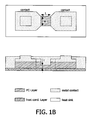
Figure 1 , the current I will flow between the outer contacts or electrodes, here composed of an Al, WTi/TiN stack, through a central part formed in the phase-change material. This shape of the memory cell results in a local increase of the current density and hence in an increased heat generation due the Joule effect. During the device operation, this constricted area with the highest current density will be the first to melt. - Instead of reducing the cross-sectional area of the central part by reducing the width W thereof as shown in
figure 1 , a constriction in vertical direction, as disclosed in the Haring Bolivar paper, can be obtained by using a local thinning of the PCM layer thereby locally reducing the thickness t of the phase-change material. - The problem is that with scaling down the dimensions, both methods for geometrically confining the first-to-melt region are prone to process variations. The control of the geometry of the hourglass shape of
Figure 1 becomes more difficult.Figure 2 shows the rounding effect due to lithographic processing generation causing the dimensions of the processed memory cell to deviate from the dimensions of the cell as-designed. The continuous line defines the cell as-designed, while the dashed line corresponds to the perimeter of the cell after lithographic patterning. This change in geometry and the spread thereon will result in larger variations of cell characteristics. The approach whereby the phase-change film thickness is reduced by etch as described in the Haring Bolivar paper is also not a well controlled process and will add to the variation. - There is a need for a more controllable method to form a phase-change-memory cell having a well-defined region of limited dimensions ("hot spot") resulting in a local increase of the current density during operation in this hot spot.
- According to a first aspect of the invention there is provided a phase-change-memory cell comprising two insulated regions formed in a first phase-change material connected by a region formed in a second phase-change material whereby the crystallization temperature of the second phase-change material is below the crystallization temperature of the first phase-change material. This provides a solution to the problem described above that includes locally changing the material properties using a second PCM material, which switches phase at a lower temperature, e.g., the amount of energy needed to initiate the phase-change process is less for the second phase-change material compared to the first phase-change material. For a given current density, the region containing this second PCM material will first melt and hence a localized "hot spot" is obtained.
- According to a second aspect of the invention there is provided a method for forming a phase-change-memory cell comprising two insulated regions formed in a first phase-change material connected by a region formed in a second phase-change material whereby the crystallization temperature of the second phase-change material is below the crystallization temperature of the first phase-change material, the method comprising:
- forming two insulated regions in a first phase-change material; and
- forming a region in a second phase-change material connecting the two insulated regions, wherein the crystallization temperature of the second phase-change material is below the crystallization temperature of the first phase-change material.
- Embodiments of the present invention will now be described, by way of example only, with reference to the accompanying drawings, in which:-
-
Figure 1A shows a schematic cross-section and scanning electron micrograph of an example type of a PCM line cell with TiN contacts and Al bond-pads processed on a silicon wafer; -
Figure 1B shows a schematic cross-section and plan view of an example type of a PCM line cell; -
Figure 2 shows a schematic plan view of part of a PCM cell; -
Figure 3 shows a schematic plan view of part of a PCM cell during manufacture in accordance with the invention; -
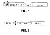
Figure 4 is a schematic cross-section showing thinning of the active region during manufacture of the PCM cell in accordance with the invention; and; -
Figure 5 is schematic top view of the active region in a second embodiment of the invention. - The process in accordance with the invention can be implemented as follows. A layer of a first PCM material such as GST225 is deposited on a substrate. This first PCM layer is patterned a first time, e.g. in the hourglass shape as shown in
Figure 2 . In this first patterning step a removable hardmask such as TiW can be used. This hardmask is formed over the first PCM layer and patterned. In turn, the patterned hardmask is used to pattern the underlying first PCM layer. A second mask (Fig. 3 ) is then used to define the active region ("hot spot") or the first-to-melt region within this first patterned PCM layer. The first PCM layer is thus patterned a second time to remove a section of the central part in the PCM cell, thereby creating two insulated regions of the first PCM material. Again, a hardmask layer such as TiW can be used in this second patterning step in similar fashion as was done in the first patterning step. In an alternative embodiment, both the first and the second mask ofFig. 3 are combined into a single mask defining both insulated parts in one single patterning step. - If present, the hardmask layer is then selectively removed. A layer of second PCM material is then deposited which crystallizes at a temperature below the temperature of the first PCM layer. This second PCM layer can be Ge4. As this second PCM layer is deposited in a separate deposition step, its thickness can be chosen independently of the thickness of the first PCM layer. Whatever the thickness t2 of the second PCM layer, the cross-sectional area in a direction perpendicular to the current flow path is reduced (
Fig.4 ), and as the resistivity of the second PCM layer is selected to be the same as or less than the resistivity of the first PCM layer, this decreased cross-sectional area would result in an increase of the current density within this second PCM layer compared to the first PCM layer. - The second PCM layer is then patterned to form a conductive path between two corresponding insulated regions of the first PCM material. For the first considered option, the same hourglass mask as in the first patterning step may be used (e.g., the first mask). In this case, a stack of two PCM layers is formed with the layers aligned to each other.
- Although this patterned second PCM layer will extend from one insulated region to another insulated region that is formed in the first PCM layer, thereby bridging the gap separating the first PCM regions, its width W2 can be made less than the width W1 of the gap (
Fig. 5 ). This way, the current density can be increased in this second PCM layer compared to the first PCM layer. This solution, which uses an additional mask, can be considered for the second option, wherein a different mask is used to pattern the second PCM layer. If present, the hardmask layer is then selectively removed. - The benefit of this new integration flow is that the material and geometry factors are combined to improve the controllability and, thus, the uniformity and reproducibility of cell characteristics.
- The PCM material Ge4 located in the active region, e.g., the region constituting the "hot spot", melts, e.g., recrystallizes, at a lower temperature (thereby requiring a lower current density) than the
PCM material GST 225 connecting the active region to the electrodes. The cross-sectional area is reduced in the active region not only in the width W (due to hourglass shape), but also in the thickness t because of the removal ofGST 225 in the active region as shown inFig. 4 . Note that forming a thin layer by deposition is more controllable than by reducing the thickness of an as-deposited layer by a post etch process. - A benefit of this increased control is that melting will substantially only occur in the active area, and this melting will occur with a lower statistical spread of characteristics.
- An additional benefit is that we reduce the risks of melt occurrence at the interface between the electrode and the phase-change material, which, if not reduce would likely result in segregation and/or a degradation in reliability. This benefit is substantially realized by using GST 225 in the periphery.
Claims (11)
- A phase-change-memory cell comprising two insulated regions formed in a first phase-change material connected by a region formed in a second phase-change material whereby the crystallization temperature of the second phase-change material is below the crystallization temperature of the first phase-change material.
- The memory cell of claim 1 whereby the cross-sectional area of the connecting region is less than the cross-sectional area of the insulated regions whereby the cross-section is taken in a direction perpendicular to the direction defined by the insulated regions.
- The memory cell of claim 2 whereby the width (W2) of the cross-sectional area of the connecting region is less than the width (W1) of the cross-sectional area of the insulated regions.
- The memory cell of claim 2 or 3, whereby the height (t2) of the cross-sectional area of the connecting region is less than the height (t1) of the cross-sectional area of the insulated regions.
- A method for forming a phase-change-memory cell the method comprising:- forming two insulated regions in a first phase-change material; and- forming a region in a second phase-change material connecting the two insulated regions, wherein the crystallization temperature of the second phase-change material is below the crystallization temperature of the first phase-change material.
- The method of claim 5 wherein the step of forming two insulated regions comprises:- forming a layer of the first phase-change material on a substrate; and,- patterning this layer to form the two insulated regions.
- The method of claim 6, wherein the step of patterning comprises:- a first patterning step to form a region in the first phase-change material; and,- a second patterning step separating this region into two insulated regions.
- The method of claim 6 or 7, wherein the step of forming the connecting region comprises:- forming a layer of the second phase-change material over the patterned layer of the first phase-change material; and,- patterning this second layer to form a region connecting the two insulated regions.
- The method of claim 8, wherein the second layer is patterned using the same mask as used in the first patterning step of claim 7.
- The method of claim 8, wherein the second layer is patterned such that the width (W2) of the cross-sectional area of the connecting region is less than the width (W1) of the cross-sectional area of the insulated regions
- The memory cell of claim 1, whereby the second phase-change material is the same as the first phase-change material
Applications Claiming Priority (2)
| Application Number | Priority Date | Filing Date | Title |
|---|---|---|---|
| US68345905P | 2005-05-19 | 2005-05-19 | |
| PCT/IB2006/051575 WO2006123305A1 (en) | 2005-05-19 | 2006-05-18 | Method for controlling the 'first-to-melt' region in a pcm cell and devices obtained thereof |
Publications (3)
| Publication Number | Publication Date |
|---|---|
| EP1886317A1 EP1886317A1 (en) | 2008-02-13 |
| EP1886317B1 true EP1886317B1 (en) | 2009-01-07 |
| EP1886317B8 EP1886317B8 (en) | 2009-04-08 |
Family
ID=36942608
Family Applications (1)
| Application Number | Title | Priority Date | Filing Date |
|---|---|---|---|
| EP06744974A Expired - Lifetime EP1886317B8 (en) | 2005-05-19 | 2006-05-18 | Method for controlling the "first-to-melt" region in a pcm cell and devices obtained thereof |
Country Status (7)
| Country | Link |
|---|---|
| US (1) | US8008644B2 (en) |
| EP (1) | EP1886317B8 (en) |
| JP (1) | JP4862113B2 (en) |
| CN (1) | CN101213612B (en) |
| AT (1) | ATE420440T1 (en) |
| DE (1) | DE602006004729D1 (en) |
| WO (1) | WO2006123305A1 (en) |
Cited By (1)
| Publication number | Priority date | Publication date | Assignee | Title |
|---|---|---|---|---|
| US8649213B2 (en) | 2008-04-01 | 2014-02-11 | Nxp B.V. | Multiple bit phase change memory cell |
Families Citing this family (7)
| Publication number | Priority date | Publication date | Assignee | Title |
|---|---|---|---|---|
| US9142763B2 (en) | 2007-06-20 | 2015-09-22 | Taiwan Semiconductor Manufacturing Co., Ltd. | Electronic component, and a method of manufacturing an electronic component |
| US8558213B2 (en) | 2008-04-01 | 2013-10-15 | Nxp B.V. | Vertical phase change memory cell |
| US8735862B2 (en) | 2011-04-11 | 2014-05-27 | Micron Technology, Inc. | Memory cells, methods of forming memory cells and methods of forming memory arrays |
| US8932900B2 (en) | 2011-08-24 | 2015-01-13 | Taiwan Semiconductor Manufacturing Company, Ltd. | Phase change memory and method of fabricating same |
| CN103346258B (en) * | 2013-07-19 | 2015-08-26 | 中国科学院上海微系统与信息技术研究所 | Phase-change memory cell and preparation method thereof |
| US10103325B2 (en) * | 2016-12-15 | 2018-10-16 | Winbond Electronics Corp. | Resistance change memory device and fabrication method thereof |
| US20210288250A1 (en) * | 2020-03-13 | 2021-09-16 | International Business Machines Corporation | Phase Change Memory Having Gradual Reset |
Family Cites Families (8)
| Publication number | Priority date | Publication date | Assignee | Title |
|---|---|---|---|---|
| US6809401B2 (en) * | 2000-10-27 | 2004-10-26 | Matsushita Electric Industrial Co., Ltd. | Memory, writing apparatus, reading apparatus, writing method, and reading method |
| US6566700B2 (en) * | 2001-10-11 | 2003-05-20 | Ovonyx, Inc. | Carbon-containing interfacial layer for phase-change memory |
| DE60137788D1 (en) * | 2001-12-27 | 2009-04-09 | St Microelectronics Srl | Architecture of a non-volatile phase change memory matrix |
| US7151273B2 (en) * | 2002-02-20 | 2006-12-19 | Micron Technology, Inc. | Silver-selenide/chalcogenide glass stack for resistance variable memory |
| KR100543445B1 (en) * | 2003-03-04 | 2006-01-23 | 삼성전자주식회사 | Phase change memory device and its formation method |
| KR100532462B1 (en) * | 2003-08-22 | 2005-12-01 | 삼성전자주식회사 | Programming method of controlling the amount of writing current of phase change memory device and writing driver circuit thereof |
| KR100569550B1 (en) * | 2003-12-13 | 2006-04-10 | 주식회사 하이닉스반도체 | Phase change resistance cell and nonvolatile memory device using same |
| JP2008541475A (en) * | 2005-05-19 | 2008-11-20 | コーニンクレッカ フィリップス エレクトロニクス エヌ ヴィ | Method for controlling "pre-melting" region in PCM cell and apparatus obtained thereby |
-
2006
- 2006-05-18 EP EP06744974A patent/EP1886317B8/en not_active Expired - Lifetime
- 2006-05-18 AT AT06744974T patent/ATE420440T1/en not_active IP Right Cessation
- 2006-05-18 DE DE602006004729T patent/DE602006004729D1/en not_active Expired - Lifetime
- 2006-05-18 WO PCT/IB2006/051575 patent/WO2006123305A1/en not_active Ceased
- 2006-05-18 CN CN2006800171422A patent/CN101213612B/en not_active Expired - Lifetime
- 2006-05-18 US US11/914,645 patent/US8008644B2/en active Active
- 2006-05-18 JP JP2008511849A patent/JP4862113B2/en not_active Expired - Lifetime
Cited By (1)
| Publication number | Priority date | Publication date | Assignee | Title |
|---|---|---|---|---|
| US8649213B2 (en) | 2008-04-01 | 2014-02-11 | Nxp B.V. | Multiple bit phase change memory cell |
Also Published As
| Publication number | Publication date |
|---|---|
| JP2008541474A (en) | 2008-11-20 |
| US8008644B2 (en) | 2011-08-30 |
| CN101213612A (en) | 2008-07-02 |
| US20080265237A1 (en) | 2008-10-30 |
| DE602006004729D1 (en) | 2009-02-26 |
| EP1886317B8 (en) | 2009-04-08 |
| CN101213612B (en) | 2010-09-29 |
| JP4862113B2 (en) | 2012-01-25 |
| WO2006123305A1 (en) | 2006-11-23 |
| EP1886317A1 (en) | 2008-02-13 |
| ATE420440T1 (en) | 2009-01-15 |
Similar Documents
| Publication | Publication Date | Title |
|---|---|---|
| TWI515836B (en) | Method for forming a memory cell using a gas cluster ion beam | |
| EP1886318B1 (en) | Method for controlling the "first-to-melt" region in a pcm cell and devices obtained thereof | |
| US8030636B2 (en) | Enhanced memory density resistance variable memory cells, arrays, devices and systems including the same, and methods of fabrication | |
| KR100491978B1 (en) | Phase change memory element capable of low power operation and method for fabricating the same | |
| EP2973771B1 (en) | Sidewall-type memory cell | |
| EP1355365A2 (en) | Electrode for phase change memory device | |
| KR20040076040A (en) | Phase-change memory device having self-heater structure | |
| US9385313B2 (en) | Resistive memory cell having a reduced conductive path area | |
| KR20150132123A (en) | Resistive memory cell with reduced bottom electrode | |
| US8008644B2 (en) | Phase-change memory cell having two insulated regions | |
| US7835177B2 (en) | Phase change memory cell and method of fabricating | |
| KR101009512B1 (en) | Phase change current density control structure | |
| KR100650753B1 (en) | Phase change memory device and manufacturing method thereof | |
| US20080012079A1 (en) | Memory cell having active region sized for low reset current and method of fabricating such memory cells | |
| US11038106B1 (en) | Phase change memory cell with a metal layer | |
| US11380842B2 (en) | Phase change memory cell with second conductive layer | |
| US20090101880A1 (en) | Phase change memory devices and methods for fabricating the same | |
| US20070075434A1 (en) | Method for producing a PCM memory element and corresponding PCM memory element | |
| KR20070069767A (en) | Phase change memory device and manufacturing method thereof |
Legal Events
| Date | Code | Title | Description |
|---|---|---|---|
| PUAI | Public reference made under article 153(3) epc to a published international application that has entered the european phase |
Free format text: ORIGINAL CODE: 0009012 |
|
| 17P | Request for examination filed |
Effective date: 20071219 |
|
| AK | Designated contracting states |
Kind code of ref document: A1 Designated state(s): AT BE BG CH CY CZ DE DK EE ES FI FR GB GR HU IE IS IT LI LT LU LV MC NL PL PT RO SE SI SK TR |
|
| 17Q | First examination report despatched |
Effective date: 20080507 |
|
| GRAP | Despatch of communication of intention to grant a patent |
Free format text: ORIGINAL CODE: EPIDOSNIGR1 |
|
| DAX | Request for extension of the european patent (deleted) | ||
| GRAS | Grant fee paid |
Free format text: ORIGINAL CODE: EPIDOSNIGR3 |
|
| GRAA | (expected) grant |
Free format text: ORIGINAL CODE: 0009210 |
|
| AK | Designated contracting states |
Kind code of ref document: B1 Designated state(s): AT BE BG CH CY CZ DE DK EE ES FI FR GB GR HU IE IS IT LI LT LU LV MC NL PL PT RO SE SI SK TR |
|
| REG | Reference to a national code |
Ref country code: GB Ref legal event code: FG4D |
|
| REG | Reference to a national code |
Ref country code: CH Ref legal event code: EP |
|
| REG | Reference to a national code |
Ref country code: IE Ref legal event code: FG4D |
|
| REF | Corresponds to: |
Ref document number: 602006004729 Country of ref document: DE Date of ref document: 20090226 Kind code of ref document: P |
|
| RAP2 | Party data changed (patent owner data changed or rights of a patent transferred) |
Owner name: INTERUNIVERSITAIR MICROELEKTRONICA CENTRUM VZW Owner name: NXP B.V. |
|
| NLT2 | Nl: modifications (of names), taken from the european patent patent bulletin |
Owner name: NXP B.V. EN INTERUNIVERSITAIR MICROELEKTRONICA CEN Effective date: 20090311 |
|
| PG25 | Lapsed in a contracting state [announced via postgrant information from national office to epo] |
Ref country code: SI Free format text: LAPSE BECAUSE OF FAILURE TO SUBMIT A TRANSLATION OF THE DESCRIPTION OR TO PAY THE FEE WITHIN THE PRESCRIBED TIME-LIMIT Effective date: 20090107 Ref country code: NL Free format text: LAPSE BECAUSE OF FAILURE TO SUBMIT A TRANSLATION OF THE DESCRIPTION OR TO PAY THE FEE WITHIN THE PRESCRIBED TIME-LIMIT Effective date: 20090107 |
|
| NLV1 | Nl: lapsed or annulled due to failure to fulfill the requirements of art. 29p and 29m of the patents act | ||
| PG25 | Lapsed in a contracting state [announced via postgrant information from national office to epo] |
Ref country code: LT Free format text: LAPSE BECAUSE OF FAILURE TO SUBMIT A TRANSLATION OF THE DESCRIPTION OR TO PAY THE FEE WITHIN THE PRESCRIBED TIME-LIMIT Effective date: 20090107 Ref country code: ES Free format text: LAPSE BECAUSE OF FAILURE TO SUBMIT A TRANSLATION OF THE DESCRIPTION OR TO PAY THE FEE WITHIN THE PRESCRIBED TIME-LIMIT Effective date: 20090418 Ref country code: FI Free format text: LAPSE BECAUSE OF FAILURE TO SUBMIT A TRANSLATION OF THE DESCRIPTION OR TO PAY THE FEE WITHIN THE PRESCRIBED TIME-LIMIT Effective date: 20090107 |
|
| RAP2 | Party data changed (patent owner data changed or rights of a patent transferred) |
Owner name: IMEC Owner name: NXP B.V. |
|
| PG25 | Lapsed in a contracting state [announced via postgrant information from national office to epo] |
Ref country code: SE Free format text: LAPSE BECAUSE OF FAILURE TO SUBMIT A TRANSLATION OF THE DESCRIPTION OR TO PAY THE FEE WITHIN THE PRESCRIBED TIME-LIMIT Effective date: 20090407 Ref country code: PT Free format text: LAPSE BECAUSE OF FAILURE TO SUBMIT A TRANSLATION OF THE DESCRIPTION OR TO PAY THE FEE WITHIN THE PRESCRIBED TIME-LIMIT Effective date: 20090608 Ref country code: LV Free format text: LAPSE BECAUSE OF FAILURE TO SUBMIT A TRANSLATION OF THE DESCRIPTION OR TO PAY THE FEE WITHIN THE PRESCRIBED TIME-LIMIT Effective date: 20090107 Ref country code: AT Free format text: LAPSE BECAUSE OF FAILURE TO SUBMIT A TRANSLATION OF THE DESCRIPTION OR TO PAY THE FEE WITHIN THE PRESCRIBED TIME-LIMIT Effective date: 20090107 Ref country code: PL Free format text: LAPSE BECAUSE OF FAILURE TO SUBMIT A TRANSLATION OF THE DESCRIPTION OR TO PAY THE FEE WITHIN THE PRESCRIBED TIME-LIMIT Effective date: 20090107 Ref country code: IS Free format text: LAPSE BECAUSE OF FAILURE TO SUBMIT A TRANSLATION OF THE DESCRIPTION OR TO PAY THE FEE WITHIN THE PRESCRIBED TIME-LIMIT Effective date: 20090507 |
|
| PG25 | Lapsed in a contracting state [announced via postgrant information from national office to epo] |
Ref country code: BE Free format text: LAPSE BECAUSE OF FAILURE TO SUBMIT A TRANSLATION OF THE DESCRIPTION OR TO PAY THE FEE WITHIN THE PRESCRIBED TIME-LIMIT Effective date: 20090107 |
|
| PG25 | Lapsed in a contracting state [announced via postgrant information from national office to epo] |
Ref country code: DK Free format text: LAPSE BECAUSE OF FAILURE TO SUBMIT A TRANSLATION OF THE DESCRIPTION OR TO PAY THE FEE WITHIN THE PRESCRIBED TIME-LIMIT Effective date: 20090107 Ref country code: CZ Free format text: LAPSE BECAUSE OF FAILURE TO SUBMIT A TRANSLATION OF THE DESCRIPTION OR TO PAY THE FEE WITHIN THE PRESCRIBED TIME-LIMIT Effective date: 20090107 Ref country code: EE Free format text: LAPSE BECAUSE OF FAILURE TO SUBMIT A TRANSLATION OF THE DESCRIPTION OR TO PAY THE FEE WITHIN THE PRESCRIBED TIME-LIMIT Effective date: 20090107 |
|
| PLBE | No opposition filed within time limit |
Free format text: ORIGINAL CODE: 0009261 |
|
| STAA | Information on the status of an ep patent application or granted ep patent |
Free format text: STATUS: NO OPPOSITION FILED WITHIN TIME LIMIT |
|
| PG25 | Lapsed in a contracting state [announced via postgrant information from national office to epo] |
Ref country code: SK Free format text: LAPSE BECAUSE OF FAILURE TO SUBMIT A TRANSLATION OF THE DESCRIPTION OR TO PAY THE FEE WITHIN THE PRESCRIBED TIME-LIMIT Effective date: 20090107 Ref country code: RO Free format text: LAPSE BECAUSE OF FAILURE TO SUBMIT A TRANSLATION OF THE DESCRIPTION OR TO PAY THE FEE WITHIN THE PRESCRIBED TIME-LIMIT Effective date: 20090107 |
|
| 26N | No opposition filed |
Effective date: 20091008 |
|
| PG25 | Lapsed in a contracting state [announced via postgrant information from national office to epo] |
Ref country code: MC Free format text: LAPSE BECAUSE OF NON-PAYMENT OF DUE FEES Effective date: 20090531 |
|
| PG25 | Lapsed in a contracting state [announced via postgrant information from national office to epo] |
Ref country code: BG Free format text: LAPSE BECAUSE OF FAILURE TO SUBMIT A TRANSLATION OF THE DESCRIPTION OR TO PAY THE FEE WITHIN THE PRESCRIBED TIME-LIMIT Effective date: 20090407 |
|
| PG25 | Lapsed in a contracting state [announced via postgrant information from national office to epo] |
Ref country code: IE Free format text: LAPSE BECAUSE OF NON-PAYMENT OF DUE FEES Effective date: 20090518 |
|
| PG25 | Lapsed in a contracting state [announced via postgrant information from national office to epo] |
Ref country code: GR Free format text: LAPSE BECAUSE OF FAILURE TO SUBMIT A TRANSLATION OF THE DESCRIPTION OR TO PAY THE FEE WITHIN THE PRESCRIBED TIME-LIMIT Effective date: 20090408 |
|
| REG | Reference to a national code |
Ref country code: CH Ref legal event code: PL |
|
| PG25 | Lapsed in a contracting state [announced via postgrant information from national office to epo] |
Ref country code: CH Free format text: LAPSE BECAUSE OF NON-PAYMENT OF DUE FEES Effective date: 20100531 Ref country code: LI Free format text: LAPSE BECAUSE OF NON-PAYMENT OF DUE FEES Effective date: 20100531 |
|
| PG25 | Lapsed in a contracting state [announced via postgrant information from national office to epo] |
Ref country code: IT Free format text: LAPSE BECAUSE OF FAILURE TO SUBMIT A TRANSLATION OF THE DESCRIPTION OR TO PAY THE FEE WITHIN THE PRESCRIBED TIME-LIMIT Effective date: 20090107 |
|
| PG25 | Lapsed in a contracting state [announced via postgrant information from national office to epo] |
Ref country code: LU Free format text: LAPSE BECAUSE OF NON-PAYMENT OF DUE FEES Effective date: 20090518 |
|
| PG25 | Lapsed in a contracting state [announced via postgrant information from national office to epo] |
Ref country code: HU Free format text: LAPSE BECAUSE OF FAILURE TO SUBMIT A TRANSLATION OF THE DESCRIPTION OR TO PAY THE FEE WITHIN THE PRESCRIBED TIME-LIMIT Effective date: 20090708 |
|
| PG25 | Lapsed in a contracting state [announced via postgrant information from national office to epo] |
Ref country code: TR Free format text: LAPSE BECAUSE OF FAILURE TO SUBMIT A TRANSLATION OF THE DESCRIPTION OR TO PAY THE FEE WITHIN THE PRESCRIBED TIME-LIMIT Effective date: 20090107 |
|
| PG25 | Lapsed in a contracting state [announced via postgrant information from national office to epo] |
Ref country code: CY Free format text: LAPSE BECAUSE OF FAILURE TO SUBMIT A TRANSLATION OF THE DESCRIPTION OR TO PAY THE FEE WITHIN THE PRESCRIBED TIME-LIMIT Effective date: 20090107 |
|
| REG | Reference to a national code |
Ref country code: FR Ref legal event code: PLFP Year of fee payment: 10 |
|
| REG | Reference to a national code |
Ref country code: FR Ref legal event code: PLFP Year of fee payment: 11 |
|
| REG | Reference to a national code |
Ref country code: FR Ref legal event code: PLFP Year of fee payment: 12 |
|
| REG | Reference to a national code |
Ref country code: FR Ref legal event code: PLFP Year of fee payment: 13 |
|
| PGFP | Annual fee paid to national office [announced via postgrant information from national office to epo] |
Ref country code: DE Payment date: 20250423 Year of fee payment: 20 |
|
| PGFP | Annual fee paid to national office [announced via postgrant information from national office to epo] |
Ref country code: GB Payment date: 20250423 Year of fee payment: 20 |
|
| PGFP | Annual fee paid to national office [announced via postgrant information from national office to epo] |
Ref country code: FR Payment date: 20250423 Year of fee payment: 20 |
|
| REG | Reference to a national code |
Ref country code: DE Ref legal event code: R082 Ref document number: 602006004729 Country of ref document: DE Representative=s name: EISENFUEHR SPEISER PATENTANWAELTE RECHTSANWAEL, DE |