EP1885648B1 - Method for making nanostructures - Google Patents
Method for making nanostructures Download PDFInfo
- Publication number
- EP1885648B1 EP1885648B1 EP06794468.6A EP06794468A EP1885648B1 EP 1885648 B1 EP1885648 B1 EP 1885648B1 EP 06794468 A EP06794468 A EP 06794468A EP 1885648 B1 EP1885648 B1 EP 1885648B1
- Authority
- EP
- European Patent Office
- Prior art keywords
- layer
- catalyst
- nanostructures
- cathode
- surface layer
- Prior art date
- Legal status (The legal status is an assumption and is not a legal conclusion. Google has not performed a legal analysis and makes no representation as to the accuracy of the status listed.)
- Not-in-force
Links
Images


Classifications
-
- H—ELECTRICITY
- H01—ELECTRIC ELEMENTS
- H01J—ELECTRIC DISCHARGE TUBES OR DISCHARGE LAMPS
- H01J9/00—Apparatus or processes specially adapted for the manufacture, installation, removal, maintenance of electric discharge tubes, discharge lamps, or parts thereof; Recovery of material from discharge tubes or lamps
- H01J9/02—Manufacture of electrodes or electrode systems
- H01J9/022—Manufacture of electrodes or electrode systems of cold cathodes
- H01J9/025—Manufacture of electrodes or electrode systems of cold cathodes of field emission cathodes
-
- B—PERFORMING OPERATIONS; TRANSPORTING
- B82—NANOTECHNOLOGY
- B82Y—SPECIFIC USES OR APPLICATIONS OF NANOSTRUCTURES; MEASUREMENT OR ANALYSIS OF NANOSTRUCTURES; MANUFACTURE OR TREATMENT OF NANOSTRUCTURES
- B82Y10/00—Nanotechnology for information processing, storage or transmission, e.g. quantum computing or single electron logic
-
- B—PERFORMING OPERATIONS; TRANSPORTING
- B82—NANOTECHNOLOGY
- B82Y—SPECIFIC USES OR APPLICATIONS OF NANOSTRUCTURES; MEASUREMENT OR ANALYSIS OF NANOSTRUCTURES; MANUFACTURE OR TREATMENT OF NANOSTRUCTURES
- B82Y30/00—Nanotechnology for materials or surface science, e.g. nanocomposites
-
- B—PERFORMING OPERATIONS; TRANSPORTING
- B82—NANOTECHNOLOGY
- B82Y—SPECIFIC USES OR APPLICATIONS OF NANOSTRUCTURES; MEASUREMENT OR ANALYSIS OF NANOSTRUCTURES; MANUFACTURE OR TREATMENT OF NANOSTRUCTURES
- B82Y40/00—Manufacture or treatment of nanostructures
-
- C—CHEMISTRY; METALLURGY
- C01—INORGANIC CHEMISTRY
- C01B—NON-METALLIC ELEMENTS; COMPOUNDS THEREOF; METALLOIDS OR COMPOUNDS THEREOF NOT COVERED BY SUBCLASS C01C
- C01B32/00—Carbon; Compounds thereof
- C01B32/15—Nano-sized carbon materials
- C01B32/158—Carbon nanotubes
- C01B32/16—Preparation
- C01B32/162—Preparation characterised by catalysts
-
- D—TEXTILES; PAPER
- D01—NATURAL OR MAN-MADE THREADS OR FIBRES; SPINNING
- D01F—CHEMICAL FEATURES IN THE MANUFACTURE OF ARTIFICIAL FILAMENTS, THREADS, FIBRES, BRISTLES OR RIBBONS; APPARATUS SPECIALLY ADAPTED FOR THE MANUFACTURE OF CARBON FILAMENTS
- D01F9/00—Artificial filaments or the like of other substances; Manufacture thereof; Apparatus specially adapted for the manufacture of carbon filaments
- D01F9/08—Artificial filaments or the like of other substances; Manufacture thereof; Apparatus specially adapted for the manufacture of carbon filaments of inorganic material
- D01F9/12—Carbon filaments; Apparatus specially adapted for the manufacture thereof
- D01F9/127—Carbon filaments; Apparatus specially adapted for the manufacture thereof by thermal decomposition of hydrocarbon gases or vapours or other carbon-containing compounds in the form of gas or vapour, e.g. carbon monoxide, alcohols
-
- H—ELECTRICITY
- H01—ELECTRIC ELEMENTS
- H01J—ELECTRIC DISCHARGE TUBES OR DISCHARGE LAMPS
- H01J1/00—Details of electrodes, of magnetic control means, of screens, or of the mounting or spacing thereof, common to two or more basic types of discharge tubes or lamps
- H01J1/02—Main electrodes
- H01J1/30—Cold cathodes, e.g. field-emissive cathode
- H01J1/304—Field-emissive cathodes
- H01J1/3048—Distributed particle emitters
-
- H—ELECTRICITY
- H01—ELECTRIC ELEMENTS
- H01J—ELECTRIC DISCHARGE TUBES OR DISCHARGE LAMPS
- H01J31/00—Cathode ray tubes; Electron beam tubes
- H01J31/08—Cathode ray tubes; Electron beam tubes having a screen on or from which an image or pattern is formed, picked up, converted, or stored
- H01J31/10—Image or pattern display tubes, i.e. having electrical input and optical output; Flying-spot tubes for scanning purposes
- H01J31/12—Image or pattern display tubes, i.e. having electrical input and optical output; Flying-spot tubes for scanning purposes with luminescent screen
- H01J31/123—Flat display tubes
- H01J31/125—Flat display tubes provided with control means permitting the electron beam to reach selected parts of the screen, e.g. digital selection
- H01J31/127—Flat display tubes provided with control means permitting the electron beam to reach selected parts of the screen, e.g. digital selection using large area or array sources, i.e. essentially a source for each pixel group
-
- H—ELECTRICITY
- H10—SEMICONDUCTOR DEVICES; ELECTRIC SOLID-STATE DEVICES NOT OTHERWISE PROVIDED FOR
- H10K—ORGANIC ELECTRIC SOLID-STATE DEVICES
- H10K10/00—Organic devices specially adapted for rectifying, amplifying, oscillating or switching; Organic capacitors or resistors having a potential-jump barrier or a surface barrier
- H10K10/40—Organic transistors
- H10K10/46—Field-effect transistors, e.g. organic thin-film transistors [OTFT]
- H10K10/462—Insulated gate field-effect transistors [IGFETs]
- H10K10/464—Lateral top-gate IGFETs comprising only a single gate
-
- H—ELECTRICITY
- H10—SEMICONDUCTOR DEVICES; ELECTRIC SOLID-STATE DEVICES NOT OTHERWISE PROVIDED FOR
- H10K—ORGANIC ELECTRIC SOLID-STATE DEVICES
- H10K10/00—Organic devices specially adapted for rectifying, amplifying, oscillating or switching; Organic capacitors or resistors having a potential-jump barrier or a surface barrier
- H10K10/40—Organic transistors
- H10K10/46—Field-effect transistors, e.g. organic thin-film transistors [OTFT]
- H10K10/462—Insulated gate field-effect transistors [IGFETs]
- H10K10/481—Insulated gate field-effect transistors [IGFETs] characterised by the gate conductors
-
- H—ELECTRICITY
- H01—ELECTRIC ELEMENTS
- H01J—ELECTRIC DISCHARGE TUBES OR DISCHARGE LAMPS
- H01J2201/00—Electrodes common to discharge tubes
- H01J2201/30—Cold cathodes
- H01J2201/304—Field emission cathodes
- H01J2201/30446—Field emission cathodes characterised by the emitter material
- H01J2201/30453—Carbon types
- H01J2201/30469—Carbon nanotubes (CNTs)
-
- H—ELECTRICITY
- H01—ELECTRIC ELEMENTS
- H01J—ELECTRIC DISCHARGE TUBES OR DISCHARGE LAMPS
- H01J2201/00—Electrodes common to discharge tubes
- H01J2201/30—Cold cathodes
- H01J2201/319—Circuit elements associated with the emitters by direct integration
-
- H—ELECTRICITY
- H10—SEMICONDUCTOR DEVICES; ELECTRIC SOLID-STATE DEVICES NOT OTHERWISE PROVIDED FOR
- H10K—ORGANIC ELECTRIC SOLID-STATE DEVICES
- H10K85/00—Organic materials used in the body or electrodes of devices covered by this subclass
- H10K85/20—Carbon compounds, e.g. carbon nanotubes or fullerenes
- H10K85/221—Carbon nanotubes
Definitions
- the invention relates to a method for producing nanostructures on a support, in particular electrically independent nanostructures.
- the invention applies in particular to electron-emitting nanotubes in cathodic structures for flat screens.
- nanostructures we are referring to here are self-assembled structures and localized by catalytic growth on a supported catalyst. It may be, for example, nanotubes, nanofilaments or nanowires.
- the catalytic growth of nanostructures on a supported catalyst requires the use of a catalyst material that limits the diffusion of the catalyst therein, and especially at the growth temperature.
- the catalyst support must be conductive but must not electrically contact the nanostructures with each other.
- the support must therefore be discontinuous, that is to say be electrically conductive under the self-assembled structures and electrical insulation (or absent) between self-assembled structures.
- One known method for obtaining such discontinuous support is to structure the support using electronic or optical lithography techniques.
- electronic or optical lithography techniques For self-assembled structures of small size and / or high density, these techniques can be very expensive and partially effective.
- Obtaining electrically independent nanostructures on a support is particularly advantageous in the field of cathodic structures, used in cathodoluminescence display devices excited by field emission and in particular in field emission flat screens.
- the field emission excited cathodoluminescence display devices comprise a cathode, which emits electrons, and an anode, opposite the cathode, covered with a luminescent layer.
- the anode and the cathode are separated by a space where the vacuum is made.
- the cathodes used are often complex cathode structures of diode or triode type.
- the triode structures have an additional electrode called a grid that facilitates the extraction of electrons from the cathode.
- Several triode structures have already been envisaged in the prior art. We can classify them in two big families depending on the position of the gate relative to the cathode.
- a first family of triode structures groups the structures where the cathode is deposited at the bottom of holes made in an insulating layer and where the gate is located on the insulating layer. These triode structures are called type I structures.
- An example of such a triode structure is described in document [ 1 ], referenced at the end of the description, which discloses a method of manufacturing a cathodic display device. luminescence excited by field emission and is illustrated in the figure 1 .
- the figure 1 is a sectional and schematic view of a known type I cathode structure for a field emission excited cathodoluminescence display. A single transmission device is shown in this figure.
- a layer 1 of electrically insulating material is pierced with a circular hole 2 and deposited on a support 10.
- a conductive layer 3 forming a cathode and supporting a layer 4 of electron-emitting material (for example a layer of electron-emitting nanostructures such as carbon nanotubes).
- the upper face of the insulating layer 1 supports a metal layer 5 forming an electron extraction grid and surrounding the hole 2.
- a second family of triode structures groups structures where the cathode is deposited on an insulating layer and where the grid is located under the insulating layer. These triode structures are called type II structures. Such triode structures are described in documents [2] and [3].
- the figure 2 is a sectional and diagrammatic view of a type II cathode structure according to the known art, for a field emission excited cathodoluminescence display device. A single transmission device is shown in this figure.
- a layer 11 of electrically insulating material deposited on a support 20 supports on its underside a gate electrode 15 consisting of two parts flanking a cathode 13 disposed on the upper face of the layer 11 and supporting a layer 14 of emitting material. electrons.
- the stack can be made more complex at the cathode by adding a resistive layer between the cathode conductor and the emissive layer.
- the objective is to limit the current emitted by the individual transmitters in order to make the emission more uniform (see document [4]).
- the resistive layer thus has a role of regulating the emission of electrons.
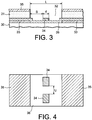
- this cathode structure comprises, in superposition on a support 30, a cathode electrode 33 in two parts in a conductive material, a resistive layer 36 covering the two parts of the cathode electrode 33 and the surface of the support 30 situated between these two parts, an insulating layer 31 and a metal layer 35 forming an electron extraction grid.
- a hole 32 of width L exposes the resistive layer 36.
- a layer of emissive material 34 formed from a growth zone, rests on the layer resistive 36.
- the width d of the growth zone of the emissive material layer 34 is small relative to the width L of the hole. This makes it possible to limit the contact possibilities of the layer of emissive material with the gate electrode, source of leakage current between cathode and gate in operation.
- the portions of the cathode electrode 33 are located vertically above the extraction grid 35. They could also be set back with respect to the grid 35.
- the growth zone can be discontinuous and structured in blocks as shown in FIG. figure 4 which is a possible top view of the cathode structure of the figure 3 . It shows that the layer of emissive material 34 is distributed on two growth pads separated by a distance U which is of the same order of magnitude as the distance S. The distribution of the emissive layer in separate pads ensures a certain electrical independence of the emitting zones with respect to each other and therefore a more effective action of the resistive layer for each pad.
- US 2004/0161929 discloses a method for producing nanostructures on a support and a cathode structure according to the preamble of claim 1.
- [10] describes a method for producing nanostructures on a support.
- the electron-emitting nanostructures should be electrically isolated from each other.
- optical lithography is used only for structures whose smallest dimension is of the order of 5 ⁇ m, whereas the radius of the emitting nanostructures is only a few nm or a few tens of nm. .
- each emitting nanostructure is electrically isolated, but groups of emitting nanostructures.
- the problem of uniformity of the electric current is not solved within the same group of emitting nanostructures, because the stud on which they rest is conductive.
- the object of the invention is to propose a method which makes it possible to obtain nanostructures on a support, and in particular electrically connected and independent nanostructures, said method being effective and less expensive than the methods known from the prior art.
- the problem that the invention seeks to solve is to obtain a structured bilayer for the growth of nanostructures in an aligned manner without using a lithography mask (resin deposition and structuring by exposure ...), or mask alignment.
- This object is achieved by a method of producing nanostructures on a support according to claim 1.
- barrier layer a layer of a material limiting the diffusion of the catalyst material attached to the barrier layer, especially the growth temperature of the nanostructures on the catalyst.
- the nanostructures obtained may be nanotubes, nanofilaments or nanowires.
- the catalyst layer is used as an etching mask.
- the step of etching the surface layer in areas not covered by the catalyst is a selective and anisotropic etching of the surface layer using the catalyst particles as an etching mask. Etching is continued until the surface layer disappears in the areas not covered by the catalyst.
- the surface layer is made of conductive or semiconductive material and the nanostructures are made of a conductive or semi-conductive material. Electrically independent nanostructures are thus obtained.
- the support comprises a resistive layer on the face intended to support the surface layer.
- resistive layer is meant a layer of a material having a resistivity and a thickness allowing it to limit or regulate the electron flow therethrough.
- the resistive layer makes it possible to limit or regulate the current emitted by the nanostructures, and all the more so that the current is important, in order to make the emission of electrons more uniform.
- the support comprises a layer of conductive material in contact with the resistive layer.
- the layer of conductive material may for example be under the resistive layer.
- At least a portion of the thickness of the resistive layer is etched in the areas where the surface layer is etched.
- structuring of the catalyst layer in a pattern is achieved by fragmenting a catalyst film on the surface layer.
- the catalyst film can be initially continuous.
- the catalyst film may also be initially discontinuous, but in this case, the step of structuring by fragmentation of the catalyst layer is not mandatory.
- the fragmentation of the catalyst film on the surface layer is obtained by increasing the temperature of the catalyst film.
- the temperature increase of the catalyst film is global, for example by annealing.
- the increase in the temperature of the catalyst film is localized on the surface, for example by laser irradiation or by plasma effect.
- the surface layer is made of a material that promotes the fragmentation of the catalyst film.
- the fragmentation of the catalyst film on the surface layer is obtained by dry or wet inhomogeneous etching techniques of the catalyst film. In other words, only certain areas are graved, for example at the grain boundaries.
- the pattern of the structured catalyst layer is adjusted before carrying out the step of etching the surface layer.
- the pattern of the catalyst layer is adjusted by etching the catalyst layer.
- the pattern of the catalyst layer is adjusted by etching said catalyst layer after carrying out the step of etching the surface layer. This makes it possible to adjust the morphology of the nanostructures.
- the pattern of the catalyst layer is adjusted, at first, by etching said catalyst layer before carrying out the etching step of the surface layer and, in a second step, by etching of said catalyst layer after having etched the surface layer.
- the selective growth of the nanostructures on the catalyst is carried out by chemical vapor deposition (CVD), assisted or not by plasma.
- CVD chemical vapor deposition
- the step of etching the surface layer is performed after the step of selective growth of the nanostructures.
- the surface layer is a barrier layer for the diffusion of the catalyst towards the support.
- the invention also relates to a cathode structure according to claim 17.
- the conductive cathode layer is disposed at the bottom of at least one hole made in a layer of electrically insulating material; the conductive layer forming a cathode supports the resistive layer, itself supporting the electron-emitting zone comprising the nanostructures, and the upper face of said layer of electrically insulating material supports the metal layer forming an extraction grid.
- the conductive cathode layer and the electron-emitting zone comprising nanostructures are arranged laterally relative to one another and separated by the resistive layer; the extraction gate metal layer is separated from the conductive cathode layer by a layer of electrical insulator.
- the resistive layer which is interposed between the conductive layer forming the cathode and the emitting zone, makes it possible to connect them electrically.
- a layer of electrically insulating material supports on its underside the metal layer forming extraction grid divided into two parts and surrounding the layer of conductive material forming a cathode disposed on the upper face of the layer of electrically insulating material, said conductive cathode layer carrying a resistive layer, itself supporting the electron emitting zone.
- the invention also relates to a flat field emission screen according to claim 21.
- a surface layer 101 is deposited on one side of a support 100, for example a glass substrate.
- this layer is a barrier layer, that is to say a material which limits the diffusion of the catalyst towards the substrate (especially at the growth temperature of the nanostructures).
- the barrier layer must be electrically conductive because the electrical addressing of the nanostructures is via their support, here the layer of surface.
- the surface layer be of a material promoting dewetting.
- it is chosen to deposit a surface layer 101 of TiN with a thickness of the order of 100 nm.
- a catalyst layer 102 is deposited in Ni having a thickness of, for example, 10 nm. If fragmentation of this catalyst layer is to be obtained by dewetting, the thickness of the catalyst layer must be less than a given threshold, known to those skilled in the art, depending on the materials used and studied for example in document [5]. Typically, to obtain a dewetting of Ni on TiN at 600 ° C., the thickness of Ni must be less than or equal to 10 nm.
- the deposits of the TiN layer 101 and the Ni layer 102 may, for example, be obtained by cathode sputtering and evaporation under vacuum, respectively.
- the structuring of the catalyst layer 102 is carried out so that it has a pattern comprising solid areas in which the catalyst is present and areas in which the catalyst has disappeared to update the underlying surface layer 101 ( figure 5b ).
- the solid areas form what are called growth zones where the nanostructures will grow.
- This structuring can be done by fragmentation of the catalyst layer on the surface layer.
- the fragmentation can be obtained by increasing the overall temperature of the stack (for example by annealing) or localized at the surface (for example by laser irradiation or with the aid of a plasma). It should be noted that fragmentation will only occur provided that the couple (barrier-catalyst layer) is such that the difference in surface energy of the two materials is sufficient to allow fragmentation by dewetting.
- annealing at 600 ° C. under a pressure of 0.2 mbar of hydrogen is suitable for a 10 nm Ni layer.
- the fragmentation can also be obtained by dry inhomogeneous etching (for example by plasma) or wet techniques of the catalyst layer 102.
- DC plasma etching of NH 3 at 390 ° C. can fragment a film of Ni (see FIG. for example the documents [6] and [7] cited at the end of the description).
- the catalyst layer 102 may be initially discontinuous or structured.
- electrochemical deposition see document [8]
- Volmer-Weber mode the deposition of aggregates or discontinuous growth
- the surface layer 101 is selectively and anisotropically etched. 101 using the catalyst as an etching mask: the surface layer 101 is etched in the areas not covered by the catalyst layer 102.
- suitable pattern is meant a pattern in which the growth zones of the nanostructures are disposed at the locations where the We want the nanostructures to grow, but especially have dimensions and a density adapted to the type of nanostructures that we want to grow.
- the pattern will represent catalyst islands, i.e. ovoid-shaped heaps, randomly dispatched to the barrier layer so as to obtain elliptical base nanostructures.
- the support substrate then comprises islands of catalyst 202 on islands of surface layer 201 ( figure 5c ).
- the anisotropic and selective etching can be obtained by using an SF 6 RIE plasma: the TiN surface layer 101 is etched in a directional manner (anisotropic etching) and the Ni catalyst islands 202. are not etched (selective etching), as well as the islands of surface layer 201 (TiN surface layer covered by the catalyst Ni).
- the density and the size distribution of the islands of catalyst 202, obtained after the structuring step can be adjusted by means of a dry or wet etching of part of the catalyst. We can thus obtain islands of catalyst of determined diameter and density.
- This etching adjustment can be performed between the structuring and etching steps of the surface layer 101, and / or between the etching steps of the surface layer 101 and the selective growth of the nanostructures. In the latter case, smaller catalyst pads are obtained than the pads of the surface layer on which it rests, which can in certain cases ensure a greater stability of the nanostructure.
- the sample can be dipped into a chemical etching solution of the catalyst for a specified period of time.
- a solution that selectively attacks the catalyst and that does not prevent the catalyst from reacting with the precursors (gaseous in the case of growth by CVD) of the nanostructures whose catalyzing it will subsequently have to catalyze. growth For example, a solution made by mixing a volume of nitric acid, a volume of acetic acid and four volumes of water can be used to effect the chemical etching of the catalyst for a period of 45 seconds.
- RIE plasma etching
- ICP ICP, etc.
- selective ion bombardment of the catalyst can be carried out.
- the adjustment of the density and the size distribution of the catalyst islands 202 can also be obtained by controlling the thickness initial of the catalyst layer 102 in the case where the catalyst unit is obtained by fragmenting by dewetting of an initially continuous catalyst layer.
- nanostructures 104 catalytic growth of nanostructures 104 is carried out from islands of catalysts 202.
- This growth can be of the "base growth” or “root growth” type, where the nanostructures are obtained by catalytic growth with the catalyst anchored on the support, or of the type “tip growth”("tipgrowth” in English), where the nanostructures 104 are obtained by catalytic growth with the catalyst 202 at the top of the nanostructures ( figure 5d ).
- catalytic growth can be achieved by chemical vapor deposition (CVD) of carbon by increasing the temperature to 600 ° C. under 0.2 mbar. of hydrogen, then exposing the sample to a pressure of 0.2 mbar of acetylene, still at 600 ° C, for 1 minute.
- CVD chemical vapor deposition
- the nanotubes have a length of up to several micrometers and a radius close to that of the catalyst island.
- the CVD growth has the particularity of giving rise to a population of nanotubes whose aspect ratio (length / radius) is widely dispersed as illustrated in the figure 5d where we can see nanotubes 104 of varying heights and diameters.
- the etching step of the surface layer 101 may take place after the step of growth of the nanostructures 104, provided that the etching is selective with respect to the nanostructures and that the shape of the nanotubes allows it (in in particular, it is preferable that the nanostructures be aligned perpendicular to the support).
- nanostructure any self-assembled and localized structure by catalytic growth on a supported catalyst and one of whose dimensions is nanometric, that is to say between 0.5 and 100 nm.
- Electrically independent nanostructures means nanostructures whose electrical potential is different for each nanostructure.
- nanostructures are non-electrically independent when their electric potential is the same, which is the case, for example, when they rest on a conductive support and are electrically interconnected by this support.
- the nanostructures may be nanotubes or nanofilaments or nanowires for example, generally one by nanostructure. But there can be more nanotubes or nanofilaments or nanowires per nanostructure if these elements grow from the same island of catalyst and / or on the same island of surface layer.
- nanostructures from a stack consisting simply of a support, a barrier layer and a catalyst layer.
- Other exemplary embodiments are possible, in particular by using a much more complex stack.
- a multilayer instead of the catalyst layer, for example a bilayer consisting of Fe and Mo, to promote the growth of the nanostructures.
- a stack comprising a glass support substrate, a conductive layer 403 made of cathode-type Mo and a resistive layer 406 made of Si to serve as a resistive layer (or ballast), a barrier layer 401 and a catalyst layer are produced. 402. Then, we carry out the same steps as those described above in the Figures 5a to 5d that is, the structuring step of the catalyst 402, the step of etching the barrier layer 401 and the step of growing the nanostructures 404 on the catalyst islands.
- the figure 6 represents the case where the etching of the barrier layer 401 has been stopped at the resistive layer 406. But stopping the etching on the resistive layer is not critical in this particular case. Indeed, as the resistive layer 406 is on a cathode layer 403, one can afford to burn all or part of this resistive layer, which further promotes the electrical independence of the nanostructures.
- the figure 7 illustrates the case where the entire thickness of the resistive layer 406 and the thickness of the barrier layer 401 have been etched in the areas not covered by the catalyst.
- This etching of the resistive layer can be done at the same time as the etching of the barrier layer if the etching technique used for the barrier layer is suitable for the resistive layer, or just after with another etching technique, or after the growth. nanostructures if the nanostructures allow it (as explained previously). In the examples illustrated in the Figures 6 and 7 in the end, electrically independent nanotubes are obtained, contrary to the prior art illustrated in FIG. figure 8 where only groups of nanotubes 304 can be electrically independent.
- the nanotubes 304 made by catalytic growth from catalyst 302, are arranged on blocks 500 made in a barrier layer 301, disposed on a resistive layer 306 supported by a layer
- Each block 500 is isolated from the other blocks but each block supports several nanostructures 304.
- the electrical potential at the base of each nanostructure of the same block is the same.
- the invention thus makes it possible to ensure the electrical independence of the nanostructures with respect to one another and an individualized action of the resistive layer (illustrated by the zigzag symbol symbolizing resistance in the Figures 6 and 7 ) for each nanostructure, which improves the uniformity of electron emission.
- This particular stack of a support substrate, a conductive layer forming a cathode, a resistive layer forming a ballast, a barrier layer and a catalyst layer makes it possible to produce a cathode structure for a transmission flat screen. of field.
- a cathode structure for a transmission flat screen. of field.
- FIG 9b A first example of a cathode structure according to the invention is illustrated in the figure 9b . It is a type I triode structure seen in cross section. According to figure 9a it can be seen that this cathode structure comprises, in superposition on a support 600, a cathode electrode 603 in two parts in a conductive material, a resistive layer 606 covering the two parts of the cathode electrode 603 and the surface of the support 600 located between these two parts, an insulating layer 611 and a metal layer 615 forming an electron extraction grid. A hole 620 of width L exposes the resistive layer 606.
- a stack of a width d consisting of a barrier layer 601 and a catalyst layer 602 rests on the resistive layer 606.
- the width d of the stack consisting of the barrier layer 601 and the catalyst layer 602 is small relative to the width L of the hole.
- the portions of the cathode electrode 603 are located vertically above the extraction grid 605. They could also be recessed with respect to the grid 605. The detail of a production method of this structure can be found in document [4].
- the structuring of the catalyst layer 602, the etching of the barrier layer 601 and the growth of the nanostructures 604 are carried out according to the embodiment method described above. Electrically 604 nanostructures are then obtained independent having a base made of a barrier layer 601 and a top made of catalyst 602 in a catalytic growth type "growth by the top” (see figure 9b ).
- the nanostructures 604 are electrically connected to the portions of the cathode electrode 603 via the resistive layer 606. Note that only one emitting device is shown in this figure, but the structure of cathode can understand several others.
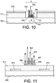
- a second example of a type I cathode structure is illustrated in the figure 10 .
- a support 700 supports a layer 711 of electrically insulating material.
- the layer 711 is pierced with a hole 720 and the upper face of the insulating layer 711 supports a metal layer 715 forming an extraction grid and surrounding the hole 720.
- a stack of width d consists of a conductive layer 703 forming a cathode supporting electrically independent nanostructures 704.
- the width d of the stack is preferably small relative to the width L of the hole.
- nanostructures 704 were obtained by carrying out the process steps according to the invention starting from an initial stack composed of a resistive layer 706, a barrier layer 701 and a catalyst layer 702. It is seen in this example that the entire thickness of the resistive layer 706 has been etched, as explained in the figure 7 .
- figure 11 represents, in sectional view and schematically, a cathode structure of type II according to the invention.
- a layer 811 of electrically insulating material supports on its underside a gate electrode 815 consisting of two parts flanking a cathode 803 disposed on the upper face of the layer 811 and supporting electrically independent nanostructures 804.
- These nanostructures 804 were obtained by carrying out the process steps according to the invention from an initial stack composed of a resistive layer 806, a barrier layer 801 and a catalyst layer 802. In this example, the entire thickness of the resistive layer 806 has been etched, as explained in figure 7 .
- a first embodiment constraint to be taken into account appears when the gate conductor of the cathode structures is not protected, as is the case in the Figures 9a and 9b , and 10 (gate driver 615 or 715). It is necessary to choose a material for the gate electrode which is not sensitive to the etching chosen for the barrier layer. For example, if a SF 6 RIE plasma is used to etch the barrier layer, a copper or aluminum gate electrode will not be etched by the plasma.
- Another constraint consists in not etching the resistive layer over its entire thickness when the cathode is disposed laterally with respect to the nanostructures, as is the case in the figure 9b . If the entire thickness of the resistive layer 606 is etched, then the nanostructures would be electrically isolated from the cathode. It is recalled that it is the resistive layer 606 which here electrically connects the nanostructures 604 to the portions of the cathode electrode 603.
- the cathode when the cathode is disposed in line with the electron-emitting nanostructures (see by example the figure 10 or the figure 11 ), one can burn the entire thickness of the resistive layer (provided however that the etching spares the electrodes below, such as the cathode and possibly the buried grid). Such etching may have the advantage of improving the isolation between the cathode and the gate conductor. For a RIE engraving of SF 6 , it is possible, for example, to choose copper or aluminum electrodes.
- Each of the cathode structures described above can be used to make a field emission flat screen.
- the cathode structure is placed opposite an anode covered with a luminescent layer, and the space separating the anode and the cathode structure is evacuated.
- nanostructures (nanotubes or nanofilaments) of carbon are preferably used as electron emitters.
- Carbon nanostructures have several advantages.
- carbon nanostructures have an important aspect ratio (length / radius) which makes it possible to amplify the electric field by a peak effect at the top of the nanostructures. It is thus possible to extract the electrons by field effect for relatively low applied electric fields.
- the carbon nanostructures have an electrical and thermal conductivity compatible with use as an electrode and they have a chemical inertia, which guarantees a good stability of their properties over time.
- carbon nanostructures can be synthesized in situ in a localized manner, over large areas and at relatively low cost.
- the carbon nanostructures have the disadvantage of having a strong distribution of the aspect ratios, which results in a strong distribution of the electric field at their apex for a given applied electric field.
- the electric current extracted by field emission depends exponentially on the electric field at the top of the emitters. It is therefore important to minimize this distribution if we want to standardize the electric current from each transmitter and get a uniform brightness on the screen, which results in increased visual quality for the screen.
- the method according to the invention it is no longer necessary to structure the barrier layer in the form of pads isolated from one another as described in document [4] and illustrated in FIG. figure 4 previously described. Indeed, it is possible to deposit a continuous strip of barrier layer since the barrier layer is then etched in the areas not covered by the catalyst.
- the nanostructures 52 according to our invention can be continuously distributed in a band of width d and still be electrically independent (see figure 13 ).
- the emitting surface of the final device is increased with respect to the prior art, while ensuring the electrical independence of the nanostructures and thereby the homogeneity of their emission.
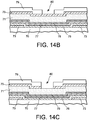
- Figures 14A to 14K illustrate the steps of this process which implements vacuum deposition and photolithography techniques.
- a stack comprising, in superposition on a support 70, a cathode electrode 73 in two parts, a resistive layer 76 covering the two parts of the cathode electrode 73, a barrier layer 77, a catalyst layer 78, an insulating layer 71, a metal layer 75 for forming an electron extraction grid, and a photosensitive resin layer 79.
- the cathode electrode 73 is obtained by depositing a conductive material, for example molybdenum, niobium, copper or ITO, on a support 70, for example glass. The deposition of conductive material is then etched into strips, typically 10 ⁇ m wide and not equal to 25 ⁇ m. It is by combining two strips that a cathode electrode 73 is formed.
- a conductive material for example molybdenum, niobium, copper or ITO
- the other layers are obtained by vacuum deposition in the following order: a resistive layer 76 having a thickness of 1.5 ⁇ m in amorphous silicon, a TiNN barrier layer 77 of approximately 100 nm and a Ni catalyst layer 78 about 10 nm, then an insulating layer 71 of 1 micron thick silica or silicon nitride, a metal layer 75 made of aluminum for forming the electron extraction grid and finally a layer 79 of photosensitive resin.
- a photolithography of the resin layer is carried out (see Figure 14B ).
- the thickness of the photosensitive resin is etched to obtain an opening 80 of about 6 ⁇ m and to expose the underlying metal layer 75 of the grid.
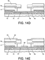
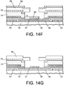
- the aluminum grid layer 75 is then chemically etched with a mixture comprising acetic acid, nitric acid and orthophosphoric acid using the resin 79 as an etching mask (see FIG. figure 14C ).
- grooves are opened in the thickness of the silica layer 71 by introducing HF through the opening made in the previous step in the grid layer ( figure 14D ). This wet etching by HF causes etching "under” the grid layer thus creating an overhang at the grid.
- a protective layer 82 of chromium is deposited by evaporation at the bottom of the opening, as well as on the layer of photoresist ( figure 14E ).
- the catalyst layer not protected by the chromium layer 82 is etched using, for example, orthophosphoric acid.
- the aluminum grid layer not covered by the silica layer (overhanging part) is also etched at the same time to save the space S (described above) between the gate and the future electron-emitting zone, and thus avoid short circuits.
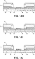
- the protective layer is then removed by etching it with a commercial mixture of perchloric acid and ammonium nitrate cerium ( figure 14G ) and the photosensitive resin is removed by "lift off” technique ( figure 14H ).
- Fragmentation of the catalyst layer is carried out to obtain catalyst islands ( figure 14I ) and the non-protected barrier layer is etched by the catalyst, for example by SF 6 RIE plasma ( Figure 14J ).
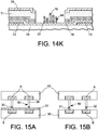
- nanostructures 84 are grown on the islands of catalyst ( figure 14K ).
- the advantage of this method is that it makes it possible to minimize the number of alignment of lithographed masks: only a mask is used to engrave the cathode electrode and a mask for etching the resin.
- the need to obtain electrically independent nanostructures may appear in any other field where the nanotubes have an electrical function and they rest on a conductive layer.
- the electrically independent nanostructures can serve as a conductive or semiconductor channel between two electrodes.
- a carbon nanotube can serve as a conductive channel and connect two different levels of metallization in a chip. This nanotube carbon should be able to withstand a current density 1000 times greater than a copper conductor channel, which is subject to electromigration induced failures (see document [9]).
- the conductive channel 50 in carbon nanotube for connecting the electrodes B of a first support 30 (for example a chip) and a second support 60 in overhang is generally made by deposition in a solid layer of a conductive barrier layer 31 on the first support 30 comprising the electrodes B, then by deposition of a catalyst pad 32 on each zone overhanging the electrodes B, and by CVD growth of carbon nanotubes 34 to connect the electrodes A of the upper bracket 60 (see figure 15a ).
- each conducting channel 50 is electrically independent of these neighbors because the barrier layer 31 at the base of each nanotube 34 is etched using the catalyst 32 as an etching mask ( figure 15b ).
- the method according to the invention has the advantage of being easy to implement, inexpensive, self-aligned (that is to say without the need for lithography mask alignment) and compatible with a wide range of applications. size range of the catalyst particles.
- the minimum size of the catalyst islands usable according to the invention is fixed by the degree of anisotropy of the etching, by its degree of selectivity, and by the thickness of the surface layer to be etched.
Description
L'invention concerne un procédé de réalisation de nanostructures sur un support, notamment des nanostructures électriquement indépendantes. L'invention s'applique en particulier aux nanotubes émetteurs d'électrons dans les structures cathodiques pour écrans plats.The invention relates to a method for producing nanostructures on a support, in particular electrically independent nanostructures. The invention applies in particular to electron-emitting nanotubes in cathodic structures for flat screens.
Les nanostructures auxquelles nous faisons référence ici sont des structures auto-assemblées et localisées par croissance catalytique sur un catalyseur supporté. Il peut s'agir par exemple de nanotubes, de nanofilaments ou de nanofils.The nanostructures we are referring to here are self-assembled structures and localized by catalytic growth on a supported catalyst. It may be, for example, nanotubes, nanofilaments or nanowires.
La croissance catalytique de nanostructures sur un catalyseur supporté impose d'utiliser, comme support du catalyseur, un matériau qui limite la diffusion du catalyseur en son sein, et notamment à la température de croissance.The catalytic growth of nanostructures on a supported catalyst requires the use of a catalyst material that limits the diffusion of the catalyst therein, and especially at the growth temperature.
Par ailleurs, si l'on souhaite obtenir des nanostructures électriquement adressables et électriquement indépendantes, le support du catalyseur doit être conducteur mais ne doit pas contacter électriquement les nanostructures entre-elles. Le support doit donc être discontinu, c'est-à-dire être conducteur électrique sous les structures auto-assemblées et isolant électrique (ou absent) entre les structures auto-assemblées.Moreover, if it is desired to obtain electrically addressable and electrically independent nanostructures, the catalyst support must be conductive but must not electrically contact the nanostructures with each other. The support must therefore be discontinuous, that is to say be electrically conductive under the self-assembled structures and electrical insulation (or absent) between self-assembled structures.
Une méthode connue pour obtenir un tel support discontinu consiste à structurer le support à l'aide de techniques de lithographie électronique ou optique. Cependant, pour des structures auto-assemblées de faible dimension et/ou de forte densité, ces techniques peuvent s'avérer très coûteuses et partiellement efficaces.One known method for obtaining such discontinuous support is to structure the support using electronic or optical lithography techniques. However, for self-assembled structures of small size and / or high density, these techniques can be very expensive and partially effective.
L'obtention de nanostructures électriquement indépendantes sur un support est particulièrement intéressante dans le domaine des structures cathodiques, utilisées dans les dispositifs de visualisation par cathodo-luminescence excités par émission de champ et en particulier dans les écrans plats à émission de champ.Obtaining electrically independent nanostructures on a support is particularly advantageous in the field of cathodic structures, used in cathodoluminescence display devices excited by field emission and in particular in field emission flat screens.
Les dispositifs de visualisation par cathodo-luminescence excités par émission de champ comprennent une cathode, qui émet des électrons, et une anode, en regard de la cathode, recouverte d'une couche luminescente. L'anode et la cathode sont séparées par un espace où le vide est fait.The field emission excited cathodoluminescence display devices comprise a cathode, which emits electrons, and an anode, opposite the cathode, covered with a luminescent layer. The anode and the cathode are separated by a space where the vacuum is made.
Les cathodes utilisées sont souvent des structures cathodiques complexes de type diode ou de type triode. Les structures triodes possèdent une électrode supplémentaire appelée grille qui facilite l'extraction des électrons de la cathode. Plusieurs structures triodes ont déjà été envisagées dans l'art antérieur. On peut les classer en deux grandes familles en fonction de la position de la grille par rapport à la cathode.The cathodes used are often complex cathode structures of diode or triode type. The triode structures have an additional electrode called a grid that facilitates the extraction of electrons from the cathode. Several triode structures have already been envisaged in the prior art. We can classify them in two big families depending on the position of the gate relative to the cathode.
Une première famille de structures triodes regroupe les structures où la cathode est déposée au fond de trous réalisés dans une couche isolante et où la grille est située sur la couche isolante. Ces structures triodes sont appelées structures de type I. Un exemple d'une telle structure triode est décrite dans le document [1], référencé à la fin de la description, qui divulgue un procédé de fabrication d'un dispositif de visualisation par cathodo-luminescence excité par émission de champ et est illustrée dans la
Une deuxième famille de structures triodes regroupe des structures où la cathode est déposée sur une couche isolante et où la grille est située sous la couche isolante. Ces structures triodes sont appelées structures de type II. De telles structures triodes sont décrites dans les documents [2] et [3]. La
Afin que les structures de cathodes de type I et II fonctionnent correctement au niveau de l'émission électronique, on peut complexifier l'empilement au niveau de la cathode en rajoutant, entre le conducteur de cathode et la couche émissive, une couche résistive dont l'objectif est de limiter le courant émis par les émetteurs individuels afin de rendre l'émission plus uniforme (voir le document [4]). La couche résistive a ainsi un rôle de régulateur de l'émission des électrons.In order for the Type I and Type II cathode structures to function correctly at the level of the electronic emission, the stack can be made more complex at the cathode by adding a resistive layer between the cathode conductor and the emissive layer. The objective is to limit the current emitted by the individual transmitters in order to make the emission more uniform (see document [4]). The resistive layer thus has a role of regulating the emission of electrons.
Une variante de réalisation d'une structure de type I est illustrée dans la
[10] décrit un procédé de réalisation de nanostructures sur un support. 1[10] describes a method for producing nanostructures on a support. 1
Idéalement, pour que la couche résistive joue pleinement son rôle individuellement pour chaque nanostructure, les nanostructures émettrices d'électrons devraient être isolées électriquement les unes des autres. Cependant, pour des raisons de coût, on ne réalise par lithographie optique que des structures dont la plus petite dimension est de l'ordre de 5 µm, tandis que le rayon des nanostructures émettrices n'est que de quelques nm ou quelques dizaines de nm.Ideally, for the resistive layer to fully play its role individually for each nanostructure, the electron-emitting nanostructures should be electrically isolated from each other. However, for cost reasons, optical lithography is used only for structures whose smallest dimension is of the order of 5 μm, whereas the radius of the emitting nanostructures is only a few nm or a few tens of nm. .
Ainsi, dans l'art antérieur, on isole électriquement non pas chaque nanostructure émettrice, mais des groupes de nanostructures émettrices. Le problème d'uniformité du courant électrique n'est pas résolu au sein d'un même groupe de nanostructures émettrices, car le plot sur lequel elles reposent est conducteur.Thus, in the prior art, not each emitting nanostructure is electrically isolated, but groups of emitting nanostructures. The problem of uniformity of the electric current is not solved within the same group of emitting nanostructures, because the stud on which they rest is conductive.
Le but de l'invention est de proposer un procédé qui permette d'obtenir des nanostructures sur un support, et en particulier des nanostructures électriquement connectées et indépendantes, ledit procédé étant efficace et moins coûteux que les procédés connus de l'art antérieur.The object of the invention is to propose a method which makes it possible to obtain nanostructures on a support, and in particular electrically connected and independent nanostructures, said method being effective and less expensive than the methods known from the prior art.
De façon plus générale, le problème que cherche à résoudre l'invention est d'obtenir un bicouche structuré pour la croissance de nanostructures de façon alignée sans utiliser de masque de lithographie (dépôt et structuration de résine par insolation...), ni d'alignement de masque.More generally, the problem that the invention seeks to solve is to obtain a structured bilayer for the growth of nanostructures in an aligned manner without using a lithography mask (resin deposition and structuring by exposure ...), or mask alignment.
Ce but est atteint par un procédé de réalisation de nanostructures sur un support selon la renvendication 1.This object is achieved by a method of producing nanostructures on a support according to
Dans notre invention, on entend par « couche barrière » une couche en un matériau limitant la diffusion du matériau catalyseur accolé à la couche barrière, notamment à la température de croissance des nanostructures sur le catalyseur.In our invention, the term "barrier layer" a layer of a material limiting the diffusion of the catalyst material attached to the barrier layer, especially the growth temperature of the nanostructures on the catalyst.
Les nanostructures obtenues peuvent être des nanotubes, des nanofilaments ou des nanofils.The nanostructures obtained may be nanotubes, nanofilaments or nanowires.
Pour l'étape de gravure, on utilise la couche de catalyseur comme masque de gravure. L'étape de gravure de la couche de surface dans les zones non couvertes par le catalyseur est une gravure sélective et anisotrope de la couche de surface en utilisant les particules de catalyseur comme masque de gravure. On poursuit la gravure jusqu' à ce que la couche de surface disparaisse dans les zones non couvertes par le catalyseur.For the etching step, the catalyst layer is used as an etching mask. The step of etching the surface layer in areas not covered by the catalyst is a selective and anisotropic etching of the surface layer using the catalyst particles as an etching mask. Etching is continued until the surface layer disappears in the areas not covered by the catalyst.
Avantageusement, la couche de surface est en matériau conducteur ou semi-conducteur et les nanostructures sont en un matériau conducteur ou semi-conducteur. On obtient ainsi des nanostructures électriquement indépendantes.Advantageously, the surface layer is made of conductive or semiconductive material and the nanostructures are made of a conductive or semi-conductive material. Electrically independent nanostructures are thus obtained.
Avantageusement, le support comporte une couche résistive sur la face destinée à supporter la couche de surface. On entend par couche résistive une couche en un matériau ayant une résistivité et une épaisseur lui permettant de limiter ou de réguler le flux d'électrons le traversant. Dans le cas de nanostructures émettrices d'électrons, par exemple, la couche résistive permet de limiter ou de réguler le courant émis par les nanostructures, et ce d'autant plus que le courant est important, afin de rendre l'émission d'électrons plus uniforme.Advantageously, the support comprises a resistive layer on the face intended to support the surface layer. By resistive layer is meant a layer of a material having a resistivity and a thickness allowing it to limit or regulate the electron flow therethrough. In the case of electron-emitting nanostructures, for example, the resistive layer makes it possible to limit or regulate the current emitted by the nanostructures, and all the more so that the current is important, in order to make the emission of electrons more uniform.
Selon une variante, le support comporte une couche de matériau conducteur en contact avec la couche résistive. La couche de matériau conducteur peut par exemple être sous la couche résistive.According to a variant, the support comprises a layer of conductive material in contact with the resistive layer. The layer of conductive material may for example be under the resistive layer.
Avantageusement, au moins une partie de l'épaisseur de la couche résistive est gravée dans les zones où la couche de surface est gravée.Advantageously, at least a portion of the thickness of the resistive layer is etched in the areas where the surface layer is etched.
Selon un exemple, la structuration de la couche de catalyseur selon un motif est obtenue par fragmentation d'un film de catalyseur sur la couche de surface. Le film de catalyseur peut être initialement continu. Le film de catalyseur peut également être initialement discontinu, mais dans ce cas, l'étape de structuration par fragmentation de la couche de catalyseur n'est pas obligatoire.In one example, structuring of the catalyst layer in a pattern is achieved by fragmenting a catalyst film on the surface layer. The catalyst film can be initially continuous. The catalyst film may also be initially discontinuous, but in this case, the step of structuring by fragmentation of the catalyst layer is not mandatory.
Avantageusement, la fragmentation du film de catalyseur sur la couche de surface est obtenue par augmentation de la température du film de catalyseur.Advantageously, the fragmentation of the catalyst film on the surface layer is obtained by increasing the temperature of the catalyst film.
Selon une variante, l'augmentation de température du film de catalyseur est globale, par exemple par recuit.According to one variant, the temperature increase of the catalyst film is global, for example by annealing.
Selon une autre variante, l'augmentation de la température du film de catalyseur est localisée en surface, par exemple par irradiation laser ou par effet plasma.According to another variant, the increase in the temperature of the catalyst film is localized on the surface, for example by laser irradiation or by plasma effect.
Avantageusement, la couche de surface est en un matériau favorisant la fragmentation du film de catalyseur.Advantageously, the surface layer is made of a material that promotes the fragmentation of the catalyst film.
Selon une autre variante, la fragmentation du film de catalyseur sur la couche de surface est obtenue par des techniques de gravure inhomogène sèche ou humide du film de catalyseur. En d'autres termes, on grave uniquement certains endroits, par exemple au niveau des joints de grains.According to another variant, the fragmentation of the catalyst film on the surface layer is obtained by dry or wet inhomogeneous etching techniques of the catalyst film. In other words, only certain areas are graved, for example at the grain boundaries.
Selon une première variante, le motif de la couche de catalyseur structurée est ajusté avant d'effectuer l'étape de gravure de la couche de surface. Avantageusement, le motif de la couche de catalyseur est ajusté par gravure de la couche de catalyseur.According to a first variant, the pattern of the structured catalyst layer is adjusted before carrying out the step of etching the surface layer. Advantageously, the pattern of the catalyst layer is adjusted by etching the catalyst layer.
Selon une deuxième variante, le motif de la couche de catalyseur est ajusté par gravure de ladite couche de catalyseur après avoir effectué l'étape de gravure de la couche de surface. Cela permet d'ajuster la morphologie des nanostructures.According to a second variant, the pattern of the catalyst layer is adjusted by etching said catalyst layer after carrying out the step of etching the surface layer. This makes it possible to adjust the morphology of the nanostructures.
Selon une troisième variante, le motif de la couche de catalyseur est ajusté, dans un premier temps, par gravure de ladite couche de catalyseur avant d'effectuer l'étape de gravure de la couche de surface et dans un deuxième temps, par gravure de ladite couche de catalyseur après avoir effectué la gravure de la couche de surface.According to a third variant, the pattern of the catalyst layer is adjusted, at first, by etching said catalyst layer before carrying out the etching step of the surface layer and, in a second step, by etching of said catalyst layer after having etched the surface layer.
Avantageusement, la croissance sélective des nanostructures sur le catalyseur est réalisée par dépôt chimique en phase vapeur (CVD), assisté ou non par plasma.Advantageously, the selective growth of the nanostructures on the catalyst is carried out by chemical vapor deposition (CVD), assisted or not by plasma.
En variante, l'étape de gravure de la couche de surface est effectuée après l'étape de croissance sélective des nanostructures.As a variant, the step of etching the surface layer is performed after the step of selective growth of the nanostructures.
Avantageusement, la couche de surface est une couche barrière à la diffusion du catalyseur vers le support.Advantageously, the surface layer is a barrier layer for the diffusion of the catalyst towards the support.
L'invention concerne également une structure de cathode selon la revendication 17. Selon un premier exemple, la couche conductrice formant cathode est disposée au fond d'au moins un trou réalisé dans une couche en matériau électriquement isolant ; la couche conductrice formant cathode supporte la couche résistive, elle-même supportant la zone émettrice d'électrons comprenant les nanostructures, et la face supérieure de ladite couche en matériau électriquement isolant supporte la couche métallique formant grille d'extraction.The invention also relates to a cathode structure according to claim 17. According to a first example, the conductive cathode layer is disposed at the bottom of at least one hole made in a layer of electrically insulating material; the conductive layer forming a cathode supports the resistive layer, itself supporting the electron-emitting zone comprising the nanostructures, and the upper face of said layer of electrically insulating material supports the metal layer forming an extraction grid.
Selon un deuxième exemple, la couche conductrice formant cathode et la zone émettrice d'électrons comprenant des nanostructures sont disposées latéralement l'une par rapport à l'autre et séparées par la couche résistive ; la couche métallique formant grille d'extraction est séparée de la couche conductrice formant cathode par une couche d'isolant électrique. La couche résistive, qui est interposée entre la couche conductrice formant cathode et la zone émettrice, permet de les relier électriquement.According to a second example, the conductive cathode layer and the electron-emitting zone comprising nanostructures are arranged laterally relative to one another and separated by the resistive layer; the extraction gate metal layer is separated from the conductive cathode layer by a layer of electrical insulator. The resistive layer, which is interposed between the conductive layer forming the cathode and the emitting zone, makes it possible to connect them electrically.
Selon un troisième exemple, une couche en matériau électriquement isolant supporte sur sa face inférieure la couche métallique formant grille d'extraction divisée en deux parties et encadrant la couche de matériau conducteur formant cathode disposée sur la face supérieure de la couche en matériau électriquement isolant, ladite couche conductrice formant cathode supportant une couche résistive, elle-même supportant la zone émettrice d'électrons.According to a third example, a layer of electrically insulating material supports on its underside the metal layer forming extraction grid divided into two parts and surrounding the layer of conductive material forming a cathode disposed on the upper face of the layer of electrically insulating material, said conductive cathode layer carrying a resistive layer, itself supporting the electron emitting zone.
L'invention concerne également un écran plat à émission de champ selon la revendication 21.The invention also relates to a flat field emission screen according to claim 21.
L'invention sera mieux comprise et d'autres avantages et particularités apparaîtront à la lecture de la description qui va suivre, donnée à titre d'exemple non limitatif, accompagnée des dessins annexés parmi lesquels :
- la
figure 1 , déjà décrite, est une vue en coupe transversale d'une structure de cathode à couche émissive, de type triode de type I selon l'art connu, - la
figure 2 , déjà décrite, est une vue en coupe transversale d'une structure de cathode à couche émissive, de type triode de type II selon l'art connu, - la
figure 3 est une vue en coupe transversale d'un autre exemple de structure de cathode à couche émissive, de type I, selon l'art connu, - la
figure 4 est une vue de dessus de la structure de cathode à couche émissive, de type I, représentée à lafigure 3 , - les
figures 5a à 5d illustrent les étapes du procédé de réalisation de nanostructures selon la présente invention, - la
figure 6 est une représentation schématique selon une vue en coupe transversale d'un exemple de réalisation selon l'invention dans lequel les nanostructures sont électriquement indépendantes, - la
figure 7 est une représentation schématique selon une vue en coupe transversale d'un autre exemple de réalisation selon l'invention dans lequel les nanostructures sont électriquement indépendantes, - la
figure 8 est une représentation schématique selon une vue en coupe transversale de nanostructures sur des plots de couche barrière selon l'art antérieur, - les
figures 9a et 9b illustrent des étapes de réalisation de nanostructures électriquement indépendantes dans une structure de cathode selon l'invention, - la
figure 10 est une vue en coupe transversale d'une structure de cathode selon l'invention, - la
figure 11 est une vue en coupe transversale d'une autre structure de cathode selon l'invention, - la
figure 12 est une vue de dessus d'une structure de cathode à couche émissive, de type I, selon l'art antérieur, - la
figure 13 est une vue de dessus d'une structure de cathode à couche émissive, de type I, selon l'invention, - les
figures 14A à 14K illustrent un procédé de réalisation d'une structure de cathode de type triode selon l'invention, - les
figures 15a et 15b représentent des nanotubes jouant le rôle de canal conducteur ou semi-conducteur entre deux électrodes selon l'art antérieur et selon l'invention, respectivement.
- the
figure 1 , already described, is a cross-sectional view of a type I triode-type triode-type cathode structure according to the prior art, - the
figure 2 , already described, is a cross-sectional view of a cathode structure with an emissive layer, of type triode type II according to the known art, - the
figure 3 is a cross-sectional view of another example of a type I emissive layer cathode structure, according to the prior art, - the
figure 4 is a top view of the type I emissive cathode structure shown in FIG.figure 3 , - the
Figures 5a to 5d illustrate the steps of the process for producing nanostructures according to the present invention, - the
figure 6 is a schematic representation in a cross-sectional view of an exemplary embodiment according to the invention in which the nanostructures are electrically independent, - the
figure 7 is a schematic representation in a cross-sectional view of another embodiment of the invention in which the nanostructures are electrically independent, - the
figure 8 is a schematic representation in a cross-sectional view of nanostructures on barrier layer pads according to the prior art, - the
Figures 9a and 9b illustrate steps for producing electrically independent nanostructures in a cathode structure according to the invention, - the
figure 10 is a cross-sectional view of a cathode structure according to the invention, - the
figure 11 is a cross-sectional view of another cathode structure according to the invention, - the
figure 12 is a top view of a cathode structure with a type I emissive layer, according to the prior art, - the
figure 13 is a top view of a type I emissive cathode structure, according to the invention, - the
Figures 14A to 14K illustrate a method for producing a cathode structure of the triode type according to the invention, - the
Figures 15a and 15b represent nanotubes acting as conductive or semiconductor channel between two electrodes according to the prior art and according to the invention, respectively.
Il est à noter que, pour simplifier, les différents éléments représentés dans ces figures ne sont pas dessinés à l'échelle.It should be noted that, for simplicity, the different elements represented in these figures are not drawn to scale.
Nous allons à présent détailler un exemple d'un mode de réalisation de nanostructures électriquement indépendantes sur un support selon l'invention.We will now detail an example of an embodiment of electrically independent nanostructures on a support according to the invention.
Sur une face d'un support 100, par exemple un substrat en verre, on dépose une couche de surface 101. Avantageusement, cette couche est une couche barrière, c'est-à-dire en un matériau qui limite la diffusion du catalyseur vers le substrat (notamment à la température de croissance des nanostructures). On rappelle que, puisque l'on désire obtenir des nanostructures électriquement indépendantes et ayant une fonction de transport électrique, la couche barrière doit être électriquement conductrice car l'adressage électrique des nanostructures se fait par l'intermédiaire de leur support, soit ici la couche de surface. On peut choisir un matériau parmi TiN, TiW, TaN, Cr, Mo... pour réaliser cette couche de surface.On one side of a
De plus, si l'on souhaite que la structuration de la couche de catalyseur soit obtenue par fragmentation par démouillage de la couche de catalyseur, il est préférable que la couche de surface soit en un matériau favorisant le démouillage.In addition, if it is desired that the structuring of the catalyst layer is obtained by fragmentation by dewetting of the catalyst layer, it is preferable that the surface layer be of a material promoting dewetting.
Dans cet exemple, on choisit de déposer une couche de surface 101 en TiN d'une épaisseur de l'ordre de 100 nm.In this example, it is chosen to deposit a
Puis, par-dessus cette couche de surface 101, on dépose une couche de catalyseur 102 en Ni d'une épaisseur par exemple de 10 nm. Si la fragmentation de cette couche de catalyseur doit être obtenue par démouillage, l'épaisseur de la couche de catalyseur doit être inférieure à un seuil donné, connu de l'homme du métier, fonction des matériaux utilisés et étudié par exemple dans le document [5]. Typiquement, pour obtenir un démouillage de Ni sur TiN à 600°C, il faut que l'épaisseur de Ni soit inférieure ou égale à 10 nm. On obtient alors un empilement constitué du substrat support 100 supportant une couche de surface 101 et une couche de catalyseur 102 comme illustré dans la
Puis, on réalise la structuration de la couche de catalyseur 102 afin qu'elle présente un motif comprenant des zones pleines dans lesquelles le catalyseur est présent et des zones dans lesquelles le catalyseur a disparu pour mettre à jour la couche de surface 101 sous-jacente (
Cette structuration peut se faire par fragmentation de la couche de catalyseur sur la couche de surface. La fragmentation peut être obtenue par augmentation de température globale de l'empilement (par exemple par recuit) ou localisée en surface (par exemple par irradiation laser ou à l'aide d'un plasma). Il faut noter que la fragmentation n'aura lieu qu'à condition que le couple (couche barrière - catalyseur) soit tel que la différence d'énergie de surface des deux matériaux soit suffisante pour permettre une fragmentation par démouillage. Pour le couple de matériaux TiN-Ni, un recuit à 600°C sous une pression de 0,2 mbar d'hydrogène convient pour une couche de Ni de 10 nm.This structuring can be done by fragmentation of the catalyst layer on the surface layer. The fragmentation can be obtained by increasing the overall temperature of the stack (for example by annealing) or localized at the surface (for example by laser irradiation or with the aid of a plasma). It should be noted that fragmentation will only occur provided that the couple (barrier-catalyst layer) is such that the difference in surface energy of the two materials is sufficient to allow fragmentation by dewetting. For the pair of TiN-Ni materials, annealing at 600 ° C. under a pressure of 0.2 mbar of hydrogen is suitable for a 10 nm Ni layer.
La fragmentation peut aussi être obtenue par des techniques de gravure inhomogène sèche (par plasma par exemple) ou humide de la couche de catalyseur 102. Ainsi, une gravure par plasma DC de NH3 à 390°C peut fragmenter un film de Ni (voir par exemple les documents [6] et [7] cités à la fin de la description).The fragmentation can also be obtained by dry inhomogeneous etching (for example by plasma) or wet techniques of the
Selon une variante, la couche de catalyseur 102 peut être initialement discontinue ou structurée. Parmi les techniques connues pour déposer la couche de catalyseur directement sous forme structurée, on peut citer les dépôts électrochimiques (voir le document [8]), ou les dépôt d'agrégats ou encore la croissance discontinue, mode Volmer-Weber, qui correspond à un démouillage instantané à température ambiante pour des épaisseurs déposées très fines. Dans ce cas, on peut réaliser une étape supplémentaire pour affiner le motif qui va servir à la gravure de la couche de surface, par exemple par gravure ou recuit. Mais cette étape supplémentaire peut être superflue si le motif obtenu après dépôt est déjà adéquat.Alternatively, the
Une fois que la couche de catalyseur 102 est structurée selon un motif adéquat, on réalise une gravure sélective et anisotrope de la couche de surface 101 en utilisant le catalyseur comme masque de gravure : la couche de surface 101 est gravée dans les zones non couvertes par la couche de catalyseur 102. On entend par motif adéquat un motif dans lequel les zones de croissance des nanostructures sont disposées aux endroits où l'on veut que les nanostructures croissent, mais surtout ont des dimensions et une densité adaptées au type de nanostructures que l'on veut faire croître. En général, le motif représentera des îlots de catalyseur, c'est-à-dire des tas de forme ovoïde, dispatchés sur la couche barrière de manière aléatoire de manière à obtenir des nanostructures de base elliptique.Once the
On poursuit la gravure jusqu'à ce que la couche de surface 101 disparaisse dans les zones non couvertes par le catalyseur 102. Le substrat support comporte alors des îlots de catalyseur 202 sur des îlots de couche de surface 201 (
Pour le couple de matériaux TiN-Ni, la gravure anisotrope et sélective peut être obtenue en utilisant un plasma RIE de SF6 : la couche de surface 101 de TiN est gravée de façon directive (gravure anisotrope) et les îlots de catalyseur 202 de Ni ne sont pas gravés (gravure sélective), ainsi que les îlots de couche de surface 201 (couche de surface de TiN recouverte par le catalyseur Ni).For the pair of TiN-Ni materials, the anisotropic and selective etching can be obtained by using an SF 6 RIE plasma: the
Selon une variante, on peut ajuster la densité et la distribution de taille des îlots de catalyseur 202, obtenus après l'étape de structuration, au moyen d'une gravure sèche ou humide d'une partie du catalyseur. On peut ainsi obtenir des îlots de catalyseur de diamètre et de densité déterminés. Cet ajustement par gravure peut être réalisé entre les étapes de structuration et de gravure de la couche de surface 101, et/ou entre les étapes de gravure de la couche de surface 101 et de croissance sélective des nanostructures. Dans ce dernier cas, on obtient des plots de catalyseur plus petits que les plots de la couche de surface sur laquelle il repose, ce qui peut assurer dans certains cas une plus grande stabilité de la nanostructure.According to one variant, the density and the size distribution of the islands of
Par exemple, si on choisit de réaliser une gravure humide du catalyseur, on peut plonger l'échantillon dans une solution d'attaque chimique du catalyseur pendant une durée déterminée. Dans ce cas, on utilise de préférence une solution qui attaque sélectivement le catalyseur et qui n'empêche pas le catalyseur de réagir avec les précurseurs (gazeux dans le cas d'une croissance par CVD) des nanostructures dont il devra par la suite catalyser la croissance. Par exemple, on peut utiliser une solution réalisée en mélangeant un volume d'acide nitrique, un volume d'acide acétique et quatre volumes d'eau pour réaliser l'attaque chimique du catalyseur pendant une durée de 45 secondes.For example, if wet etching of the catalyst is chosen, the sample can be dipped into a chemical etching solution of the catalyst for a specified period of time. In this case, use is preferably made of a solution that selectively attacks the catalyst and that does not prevent the catalyst from reacting with the precursors (gaseous in the case of growth by CVD) of the nanostructures whose catalyzing it will subsequently have to catalyze. growth. For example, a solution made by mixing a volume of nitric acid, a volume of acetic acid and four volumes of water can be used to effect the chemical etching of the catalyst for a period of 45 seconds.
Si on choisit de réaliser une gravure sèche du catalyseur, on peut réaliser une gravure par plasma (RIE, ICP...) ou par bombardement ionique sélectif du catalyseur.If one chooses to carry out a dry etching of the catalyst, plasma etching (RIE, ICP, etc.) or selective ion bombardment of the catalyst can be carried out.
L'ajustement de la densité et de la distribution de taille des îlots de catalyseur 202 peut également être obtenu par contrôle de l'épaisseur initiale de la couche de catalyseur 102 dans le cas où le motif de catalyseur est obtenu par fragmentation par démouillage d'une couche de catalyseur initialement continue.The adjustment of the density and the size distribution of the
Enfin, on effectue une croissance catalytique de nanostructures 104 à partir des îlots de catalyseurs 202. Cette croissance peut être du type « croissance par la base » (en anglais « base growth » ou « root growth »), où les nanostructures sont obtenues par croissance catalytique avec le catalyseur ancré sur le support, ou du type « croissance par le sommet » (« tip growth » en anglais), où les nanostructures 104 sont obtenues par croissance catalytique avec le catalyseur 202 se retrouvant au sommet des nanostructures (
Pour obtenir des nanotubes 104 de carbone à partir d'îlots de catalyseur 202 en nickel, on peut réaliser une croissance catalytique par dépôt chimique en phase vapeur (CVD) de carbone en augmentant la température jusqu'à 600°C sous 0,2 mbar d'hydrogène, puis en exposant l'échantillon à une pression de 0,2 mbar d'acétylène, toujours à 600°C, pendant 1 minute. On obtient ainsi des nanotubes 104 de carbone sur chaque îlot de couche de surface 201 en TiN, avec un îlot de catalyseur 202 de Ni à leur sommet (croissance du type « croissance par le sommet »). Les nanotubes ont une longueur pouvant atteindre plusieurs micromètres et un rayon voisin de celui de l'îlot de catalyseur. La croissance CVD présente la particularité de donner lieu à une population de nanotubes dont le rapport d'aspect (longueur/rayon) est très dispersé comme illustré dans la
Selon une variante, l'étape de gravure de la couche de surface 101 peut avoir lieu après l'étape de croissance des nanostructures 104, à condition que la gravure soit sélective vis à vis des nanostructures et que la forme des nanotubes le permette (en particulier, il est préférable que les nanostructures soient alignées perpendiculairement au support).According to one variant, the etching step of the
L'invention présente un procédé permettant d'obtenir des nanostructures, et notamment des nanostructures électriquement indépendantes. Par « nanostructure », on entend toute structure auto-assemblée et localisée par croissance catalytique sur un catalyseur supporté et dont l'une des dimensions est nanométrique, c'est-à-dire comprise entre 0,5 et 100 nm. Par « nanostructures électriquement indépendantes », on entend des nanostructures dont le potentiel électrique est différent pour chaque nanostructure. Par opposition, des nanostructures sont non électriquement indépendantes lorsque leur potentiel électrique est le même, ce qui est le cas, par exemple, lorsqu'elles reposent sur un support conducteur et sont liées entre elles électriquement par ce support. On rappelle par ailleurs que les nanostructures peuvent être des nanotubes ou des nanofilaments ou des nanofils par exemple, en général un par nanostructure. Mais il peut y avoir plusieurs nanotubes ou nanofilaments ou nanofils par nanostructure si ces éléments croissent à partir du même îlot de catalyseur et/ou sur le même îlot de couche de surface.The invention provides a method for obtaining nanostructures, and in particular electrically independent nanostructures. By "nanostructure" is meant any self-assembled and localized structure by catalytic growth on a supported catalyst and one of whose dimensions is nanometric, that is to say between 0.5 and 100 nm. "Electrically independent nanostructures" means nanostructures whose electrical potential is different for each nanostructure. In contrast, nanostructures are non-electrically independent when their electric potential is the same, which is the case, for example, when they rest on a conductive support and are electrically interconnected by this support. It is also recalled that the nanostructures may be nanotubes or nanofilaments or nanowires for example, generally one by nanostructure. But there can be more nanotubes or nanofilaments or nanowires per nanostructure if these elements grow from the same island of catalyst and / or on the same island of surface layer.
Nous venons de détailler un exemple de formation de nanostructures à partir d'un empilement constitué simplement d'un support, d'une couche barrière et d'une couche de catalyseur. D'autres exemples de réalisation sont possibles, notamment en utilisant un empilement beaucoup plus complexe. Par exemple, on peut réaliser les mêmes étapes que précédemment en interposant une couche résistive, ou une couche conductrice surmontée d'une couche résistive, entre le substrat support et la couche barrière. Il est également possible d'utiliser un multicouche à la place de la couche de catalyseur, par exemple un bicouche constitué de Fe et Mo, pour favoriser la croissance des nanostructures.We have just described an example of forming nanostructures from a stack consisting simply of a support, a barrier layer and a catalyst layer. Other exemplary embodiments are possible, in particular by using a much more complex stack. For example, one can carry out the same steps as before by interposing a resistive layer, or a conductive layer surmounted by a resistive layer, between the support substrate and the barrier layer. It is also possible to use a multilayer instead of the catalyst layer, for example a bilayer consisting of Fe and Mo, to promote the growth of the nanostructures.
Selon un exemple particulier, on réalise un empilement comprenant un substrat support en verre, une couche conductrice 403 en Mo formant cathode et une couche résistive 406 en Si pour servir de couche résistive (ou ballast), une couche barrière 401 et une couche de catalyseur 402. Puis, on réalise les mêmes étapes que celles décrites plus haut dans les
La
Cet empilement particulier d'un substrat support, d'une couche conductrice formant cathode, d'une couche résistive formant un ballast, d'une couche barrière et d'une couche de catalyseur permet de réaliser une structure cathodique pour un écran plat à émission de champ. Nous allons présenter plusieurs exemples de structures de cathode présentant des nanostructures électriquement indépendantes et pouvant être utilisées dans un écran plat à émission de champ.This particular stack of a support substrate, a conductive layer forming a cathode, a resistive layer forming a ballast, a barrier layer and a catalyst layer makes it possible to produce a cathode structure for a transmission flat screen. of field. We will present several examples of cathode structures with electrically independent nanostructures that can be used in a field emission flat panel.
Un premier exemple d'une structure de cathode selon l'invention est illustré dans la
On réalise ensuite la structuration de la couche de catalyseur 602, la gravure de la couche barrière 601 et la croissance des nanostructures 604 selon le procédé de réalisation décrit précédemment. On obtient alors des nanostructures 604 électriquement indépendantes comportant une base faite d'une couche barrière 601 et un sommet fait de catalyseur 602 selon une croissance catalytique de type « croissance par le sommet » (voir
Un deuxième exemple d'une structure de cathode de type I est illustré dans la
Ces nanostructures 704 ont été obtenues par réalisation des étapes de procédé selon l'invention à partir d'un empilement initial composé d'une couche résistive 706, d'une couche barrière 701 et d'une couche de catalyseur 702. On voit dans cet exemple que toute l'épaisseur de la couche résistive 706 a été gravée, comme expliqué dans la
Enfin, la
Il est à noter que certaines contraintes peuvent apparaître pour l'étape de gravure de la couche barrière dans des cas précis de réalisation de structure de cathode.It should be noted that certain constraints may appear for the step of etching the barrier layer in specific cases of cathode structure realization.
Une première contrainte de réalisation à prendre en compte apparaît lorsque le conducteur de grille des structures de cathode n'est pas protégé, comme c'est le cas dans les
Une autre contrainte consiste à ne pas graver la couche résistive sur toute son épaisseur lorsque la cathode est disposée latéralement par rapport aux nanostructures, comme c'est le cas dans la
Chacune des structures de cathode décrites plus haut peuvent être utilisées pour réaliser un écran plat à émission de champ. Pour cela, on place la structure cathodique en regard d'une anode recouverte d'une couche luminescente, et l'espace séparant l'anode et la structure cathodique est mis sous vide.Each of the cathode structures described above can be used to make a field emission flat screen. For this purpose, the cathode structure is placed opposite an anode covered with a luminescent layer, and the space separating the anode and the cathode structure is evacuated.
En général, pour la fabrication d'écrans plats à émission de champ, on utilise de préférence des nanostructures (nanotubes ou nanofilaments) de carbone comme émetteurs d'électron. En effet, les nanostructures en carbone présentent plusieurs avantages.In general, for the production of field emission flat screens, nanostructures (nanotubes or nanofilaments) of carbon are preferably used as electron emitters. Indeed, Carbon nanostructures have several advantages.
Tout d'abord, les nanostructures de carbone présentent un rapport d'aspect (longueur/rayon) important qui permet d'amplifier le champ électrique par effet de pointe au sommet des nanostructures. On peut ainsi réaliser l'extraction d'électrons par effet de champ pour des champs électriques appliqués relativement faibles.Firstly, carbon nanostructures have an important aspect ratio (length / radius) which makes it possible to amplify the electric field by a peak effect at the top of the nanostructures. It is thus possible to extract the electrons by field effect for relatively low applied electric fields.
Par ailleurs, les nanostructures de carbone ont une conductivité électrique et thermique compatible avec une utilisation comme électrode et elles présentent une inertie chimique, ce qui garantit une bonne stabilité de leurs propriétés dans le temps.Furthermore, the carbon nanostructures have an electrical and thermal conductivity compatible with use as an electrode and they have a chemical inertia, which guarantees a good stability of their properties over time.
Enfin, les nanostructures de carbone peuvent être synthétisées in situ de façon localisée, sur de grandes surfaces et à relativement bas coût.Finally, carbon nanostructures can be synthesized in situ in a localized manner, over large areas and at relatively low cost.
En revanche, les nanostructures de carbone ont l'inconvénient de présenter une forte distribution des rapports d'aspect, ce qui se traduit par une forte distribution du champ électrique à leur sommet pour un champ électrique appliqué donné. Or, le courant électrique extrait par émission de champ dépend de façon exponentielle du champ électrique au sommet des émetteurs. Il est donc important de minimiser cette distribution si l'on veut uniformiser le courant électrique issu de chaque émetteur et obtenir une brillance uniforme sur l'écran, ce qui se traduit par une qualité visuelle accrue pour l'écran.On the other hand, the carbon nanostructures have the disadvantage of having a strong distribution of the aspect ratios, which results in a strong distribution of the electric field at their apex for a given applied electric field. However, the electric current extracted by field emission depends exponentially on the electric field at the top of the emitters. It is therefore important to minimize this distribution if we want to standardize the electric current from each transmitter and get a uniform brightness on the screen, which results in increased visual quality for the screen.
Dans l'art antérieur, une solution bas coût consistait à disposer une couche résistive sous la couche barrière et de regrouper les nanotubes sur des plots de couches barrière électriquement isolés les uns des autres (voir
On remarquera qu'avec le procédé selon l'invention, il n'est plus nécessaire de structurer la couche barrière sous forme de plots isolés les uns des autres tel que décrit dans le document [4] et illustré dans la
On peut ainsi envisager un nouveau procédé de réalisation d'une structure triode de type I. Les
Tout d'abord, selon la
L'électrode de cathode 73 est obtenue par dépôt d'un matériau conducteur, par exemple le molybdène, le niobium, le cuivre ou l'ITO, sur un support 70, par exemple en verre. Le dépôt de matériau conducteur est ensuite gravé en bandes, typiquement de 10 µm de largeur et de pas égal à 25 µm. C'est en associant deux bandes qu'on forme une électrode de cathode 73.The
Les autres couches sont obtenues par dépôts sous vide selon l'ordre suivant : une couche résistive 76 de 1,5 µm d'épaisseur en silicium amorphe, une couche barrière 77 de TiN d'environ 100 nm et une couche de catalyseur 78 en Ni d'environ 10 nm, puis une couche isolante 71 de 1 µm d'épaisseur en silice ou en nitrure de silicium, une couche métallique 75 en aluminium destinée à former la grille d'extraction des électrons et enfin une couche de résine 79 photosensible.The other layers are obtained by vacuum deposition in the following order: a
Puis, on effectue une photolithographie de la couche de résine (voir
On réalise ensuite une gravure chimique de la couche de grille 75 en aluminium avec un mélange comprenant de l'acide acétique, de l'acide nitrique et de l'acide orthophosphorique en utilisant la résine 79 comme masque de gravure (voir
Puis, on réalise l'ouverture de gorges dans l'épaisseur de la couche de silice 71 en introduisant du HF par l'ouverture réalisée à l'étape précédente dans la couche de grille (
On dépose ensuite par évaporation une couche protectrice 82 de chrome au fond de l'ouverture, ainsi que sur la couche de résine photosensible (
Selon la
Puis on élimine la couche protectrice en la gravant à l'aide d'un mélange commercial d'acide perchlorique et de nitrate d'ammonium cérium (
On réalise la fragmentation de la couche de catalyseur jusqu'à obtenir des îlots de catalyseur (
Enfin, on fait croître des nanostructures 84 sur les îlots de catalyseur (
L'intérêt de ce procédé est qu'il permet de minimiser le nombre d'alignement de masques lithographiés : on utilise uniquement un masque pour graver l'électrode de cathode et un masque pour graver la résine.The advantage of this method is that it makes it possible to minimize the number of alignment of lithographed masks: only a mask is used to engrave the cathode electrode and a mask for etching the resin.
Le besoin d'obtenir des nanostructures électriquement indépendantes peut apparaître dans tout autre domaine où les nanotubes ont une fonction électrique et qu'ils reposent sur une couche conductrice. Par exemple, les nanostructures électriquement indépendantes peuvent servir de canal conducteur ou semi-conducteur entre deux électrodes. Par exemple, un nanotube de carbone peut servir de canal conducteur et connecter deux niveaux de métallisation différents dans une puce. Ce nanotube de carbone devrait pouvoir supporter une densité de courant 1000 fois supérieure à un canal conducteur en cuivre, qui est soumis aux ruptures induites par électromigration (voir document [9]). The need to obtain electrically independent nanostructures may appear in any other field where the nanotubes have an electrical function and they rest on a conductive layer. For example, the electrically independent nanostructures can serve as a conductive or semiconductor channel between two electrodes. For example, a carbon nanotube can serve as a conductive channel and connect two different levels of metallization in a chip. This nanotube carbon should be able to withstand a current density 1000 times greater than a copper conductor channel, which is subject to electromigration induced failures (see document [9]).
On peut également réaliser des nanotubes servant de canal semi-conducteur pour obtenir un transistor vertical à grille coaxiale (en anglais « vertical coaxially gated CNT transistor ») (voir documents [9] et [10]). It is also possible to produce nanotubes serving as a semiconductor channel to obtain a vertical transistor with a coaxial grid (in English "vertical coaxially gated CNT transistor") (see documents [9] and [10]).
Dans l'art antérieur, le canal conducteur 50 en nanotube de carbone permettant de relier les électrodes B d'un premier support 30 (par exemple une puce) et un second support 60 en surplomb est en général réalisé par dépôt en couche pleine d'une couche barrière 31 conductrice sur le premier support 30 comprenant les électrodes B, puis par dépôt d'un plot de catalyseur 32 sur chaque zone surplombant les électrodes B, et par croissance CVD de nanotubes 34 de carbone jusqu'à relier les électrodes A du support supérieur 60 (voir
En résumé, le procédé selon l'invention présente l'avantage d'être facile à mettre en oeuvre, peu onéreux, auto aligné (c'est-à-dire sans nécessité d'alignement de masque de lithographie) et compatible avec une large gamme de dimensions des particules de catalyseur. La taille minimale des îlots de catalyseur utilisables selon l'invention est fixée par le degré d'anisotropie de la gravure, par son degré de sélectivité, et par l'épaisseur de la couche de surface à graver.In summary, the method according to the invention has the advantage of being easy to implement, inexpensive, self-aligned (that is to say without the need for lithography mask alignment) and compatible with a wide range of applications. size range of the catalyst particles. The minimum size of the catalyst islands usable according to the invention is fixed by the degree of anisotropy of the etching, by its degree of selectivity, and by the thickness of the surface layer to be etched.
-
[1]
FR-A-2 593 953 US N° 4 857 161 FR-A-2,593,953 U.S. Patent No. 4,857,161 -
[2]
FR-A-2 798 507 FR-A-2 798 507 -
[3]
FR-A-2 798 508 US N° 6 815 902 FR-A-2 798 508 U.S. Patent No. 6,815,902 -
[4]
EP 1 336 980 A1 US 2003/0184357 A1 EP 1 336 980 A1US 2003/0184357 A1 -
[5]
« The Thermodynamics and Kinetics of Film Agglomération », David J. Srolovitz et Max G. Goldiner, Journal of Metals (1995), 47(3), 31-36,76-77 "The Thermodynamics and Kinetics of Film Agglomeration", David J. Srolovitz and Max G. Goldiner, Journal of Metals (1995), 47 (3), 31-36, 76-77 -
[6]
« Control of carbon nanotubes density through Ni nanoparticle formation using thermal and NH3 plasma treatment », Jong Hyung Choi et al., Diamond and related materials (2003), 12, 794-798 "Control of carbon nanotubes through Ni nanoparticle formation using thermal and NH3 plasma treatment", Jong Hyung Choi et al., Diamond and related materials (2003), 12, 794-798 -
[7]
«Density control of carbon nanotubes using NH3 plasma treatment of Ni catalyst layer », Jong Hyung Choi et al., Thin Solid Films (2003), 435, 318-323 "Density control of carbon nanotubes using NH3 plasma treatment of Ni catalyst layer", Jong Hyung Choi et al., Thin Solid Films (2003), 435, 318-323 -
[8]
« Growth of aligned carbon nanotubes with controlled site density », Y. Tu et al., Applied Physics Letters (2002), 80(21), 4018-4020 "Growth of aligned carbon nanotubes with controlled site density", Y. Tu et al., Applied Physics Letters (2002), 80 (21), 4018-4020 -
[9]
G.S. Duesberg et al./ Diamond and Related Materials 13 (2004) 354-361 GS Duesberg et al., Diamond and Related Materials 13 (2004) 354-361 -
[10]
A.P. Graham et al. / Diamond and Related Materials 13 (2004) 1296-1300 AP Graham et al. / Diamond and Related Materials 13 (2004) 1296-1300
Claims (21)
- Process for making nanostructures (104; 404; 604; 704; 804) on a support, the process comprising the following steps:- supply of a support comprising a surface layer (101; 401; 601; 701; 801) on one of its faces;- covering of the surface layer by a catalyst layer (102; 202; 402; 602; 702; 802) structured according to a pattern exposing areas of the surface layer covered by the catalyst and areas of the surface layer not covered by the catalyst, the surface layer being a barrier layer to diffusion of the catalyst towards the support;- etching of the thickness of the surface layer (101; 401; 601; 701; 801) in all the areas not covered by the catalyst layer by using the structured catalyst layer as an etching mask, until the surface layer disappears in the areas not covered by the catalyst layer;- selective growth of nanostructures (104; 404; 604; 704; 804) on the areas of the surface layer covered by the catalyst.
- Process for making nanostructures according to claim 1, characterized in that the surface layer is made of a conducting or semi conducting material and the nanostructures are made of a conducting or semi conducting material.
- Process for making nanostructures according to claim 1 or 2, characterized in that the support comprises a resistive layer (406; 606; 706; 806) on the face that will support the surface layer (401; 601; 701; 801).
- Process for making nanostructures according to claim 3, characterized in that the support comprises a layer made of a conducting material (402; 602; 702; 802) in contact with the resistive layer.
- Process for making nanostructures according to either claim 3 or 4, characterized in that at least part of the thickness of the resistive layer is etched in the areas in which the surface layer is etched.
- Process for making nanostructures according to any one of claims 1 to 5, characterized in that the catalyst layer is structured according to a pattern obtained by fragmentation of a catalyst film on the surface layer.
- Process for making nanostructures according to claim 6, characterized in that the catalyst film on the surface layer is fragmented by increasing the temperature of the catalyst film.
- Process for making nanostructures according to claim 7, characterized in that the temperature of the catalyst film is increased globally, for example by annealing.
- Process for making nanostructures according to claim 7, characterized in that the increase of the temperature of the catalyst film is localized on the surface, for example by laser irradiation or by plasma effect.
- Process for making nanostructures according to any one of claims 6 to 9, characterized in that the surface layer is made of a material facilitating fragmentation of the catalyst film.
- Process for making nanostructures according to claim 6, characterized in that the catalyst film on the surface layer is fragmented using non-homogenous dry or wet etching techniques of the catalyst film.
- Process for making nanostructures according to any one of claims 1 to 11, characterized in that the pattern of the structured catalyst layer is adjusted before performing the etching step of the surface layer.
- Process for making nanostructures according to claim 12, characterized in that the pattern of the catalyst layer is adjusted by etching the catalyst layer.
- Process for making nanostructures according to any one of claims 1 to 13, characterized in that the pattern of the catalyst layer is adjusted by etching of the catalyst layer after performing the etching step of the surface layer.
- Process for making nanostructures according to any one of claims 1 to 14, characterized in that the selective growth of nanostructures on the catalyst is done by chemical vapor phase deposition (CVD).
- Process for making nanostructures according to any one of claims 1 to 15, characterized in that the surface layer etching step is carried out after the step for selective growth of nanostructures.
- Cathode structure comprising:- a support (600; 700; 800);- a conducting layer forming a cathode (603 ;703 ; 803) on the support;- at least one electron emitting area comprising electron emitting nanostructures (604; 704; 804) formed from a catalyst layer (602; 702; 802) covering a barrier layer (601; 701; 801) to diffusion of the catalyst, the barrier layer being supported by a resistive layer, the nanostructures being electrically connected to the conducting layer forming the cathode through the barrier layer and the resistive layer,- a metallic layer forming an extraction gate (615; 715; 815) to extract electrons emitted by the nanostructures;the cathode structure being characterized in that the nanostructures are electrically independent nanostructures obtained by structuring the catalyst layer according to a pattern comprising solid areas, in which the catalyst is present, separated by areas in which the catalyst is not present, the solid areas of the catalyst layer forming growth zones for the nanostructures, the barrier layer being absent in all the areas not covered by the catalyst and being etched to form islands separated from each other, each nanostructure having its own island.
- Cathode structure according to claim 17, wherein the conducting layer forming the cathode (703) is arranged at the bottom of at least one hole formed in a layer made of an electrically insulating material (711), the conducting layer forming the cathode supporting the resistive layer, itself supporting the electron emitting area comprising the nanostructures (704) and the upper face of the layer made of an electrically insulating material (711) supporting the metallic layer forming the extraction gate (715).
- Cathode structure according to claim 17, wherein the conducting layer forming the cathode (603) and the electron emitting area comprising nanostructures (604) are arranged one at the side of the other and separated by the resistive layer (606), the metallic layer forming the extraction gate (615) being separated from the conducting layer forming the cathode (603) by an electrically insulating layer (611).
- Cathode structure according to claim 17, wherein a layer of electrically insulating material (811) supports on its upper face the metallic layer forming the extraction gate (815) divided into two parts and surrounding the layer of conducting material forming the cathode (803) located on the upper face of the layer of electrically insulating material (811), the conducting layer forming the cathode (803) supporting the resistive layer, itself supporting the electron emitting area.
- Field emission flat screen comprising a cathode structure and an anode, covered by a luminescent layer, the anode being arranged facing the cathode structure, and the anode and the cathode structure being separated by a space in which a vacuum is created, characterized in that the cathode structure is a cathode structure according to any one of claims 17 to 20.
Applications Claiming Priority (2)
| Application Number | Priority Date | Filing Date | Title |
|---|---|---|---|
| FR0551412A FR2886284B1 (en) | 2005-05-30 | 2005-05-30 | METHOD FOR PRODUCING NANOSTRUCTURES |
| PCT/FR2006/050489 WO2007003826A2 (en) | 2005-05-30 | 2006-05-29 | Method for making nanostructures |
Publications (2)
| Publication Number | Publication Date |
|---|---|
| EP1885648A2 EP1885648A2 (en) | 2008-02-13 |
| EP1885648B1 true EP1885648B1 (en) | 2018-08-29 |
Family
ID=35520555
Family Applications (2)
| Application Number | Title | Priority Date | Filing Date |
|---|---|---|---|
| EP06820247A Withdrawn EP1885649A2 (en) | 2005-05-30 | 2006-05-29 | Method for making an emissive cathode |
| EP06794468.6A Not-in-force EP1885648B1 (en) | 2005-05-30 | 2006-05-29 | Method for making nanostructures |
Family Applications Before (1)
| Application Number | Title | Priority Date | Filing Date |
|---|---|---|---|
| EP06820247A Withdrawn EP1885649A2 (en) | 2005-05-30 | 2006-05-29 | Method for making an emissive cathode |
Country Status (5)
| Country | Link |
|---|---|
| US (2) | US7785164B2 (en) |
| EP (2) | EP1885649A2 (en) |
| JP (2) | JP5247438B2 (en) |
| FR (1) | FR2886284B1 (en) |
| WO (2) | WO2007003826A2 (en) |
Families Citing this family (15)
| Publication number | Priority date | Publication date | Assignee | Title |
|---|---|---|---|---|
| FR2873852B1 (en) | 2004-07-28 | 2011-06-24 | Commissariat Energie Atomique | HIGH RESOLUTION CATHODE STRUCTURE |
| WO2007114655A1 (en) * | 2006-04-05 | 2007-10-11 | Industry Academic Cooperation Foundation Of Kyunghee University | Field emission display and manufacturing method of the same having selective array of electron emission source |
| KR100803194B1 (en) * | 2006-06-30 | 2008-02-14 | 삼성에스디아이 주식회사 | Method of forming carbon nanutubes structure |
| KR101500462B1 (en) | 2006-12-19 | 2015-03-18 | 바스프 코팅스 게엠베하 | Coating agents having high scratch resistance and weathering stability |
| DE102007061855A1 (en) | 2007-12-19 | 2009-06-25 | Basf Coatings Ag | Coating agent with high scratch resistance and weathering stability |
| DE102007061854A1 (en) | 2007-12-19 | 2009-06-25 | Basf Coatings Ag | Coating agent with high scratch resistance and weathering stability |
| DE102007061856A1 (en) | 2007-12-19 | 2009-06-25 | Basf Coatings Ag | Coating agent with high scratch resistance and weathering stability |
| JP5187689B2 (en) * | 2008-08-08 | 2013-04-24 | 学校法人 関西大学 | Nanowire structure, nanowire conjugate, and method for producing the same |
| JP5572944B2 (en) * | 2008-12-18 | 2014-08-20 | 富士通株式会社 | Wiring structure manufacturing method and wiring structure |
| DE102009024103A1 (en) | 2009-06-06 | 2010-12-09 | Basf Coatings Gmbh | Coating compositions and coatings produced therefrom with high scratch resistance and high boiling stability |
| CN102064063B (en) * | 2010-12-24 | 2012-08-29 | 清华大学 | Field-emission cathode device and preparation method thereof |
| EP2541581A1 (en) * | 2011-06-29 | 2013-01-02 | Khalid Waqas | Device comprising nanostructures and method of manufacturing thereof |
| WO2013037951A1 (en) * | 2011-09-16 | 2013-03-21 | Danmarks Tekniske Universitet | Catalyst deposition for the preparation of carbon nanotubes |
| CN105984862B (en) * | 2015-02-16 | 2018-08-28 | 北京大学深圳研究生院 | Method for growing carbon nanotube |
| JP2022052420A (en) | 2020-09-23 | 2022-04-04 | セイコーエプソン株式会社 | Light emitting device, method for manufacturing light emitting device and projector |
Family Cites Families (46)
| Publication number | Priority date | Publication date | Assignee | Title |
|---|---|---|---|---|
| FR2593953B1 (en) | 1986-01-24 | 1988-04-29 | Commissariat Energie Atomique | METHOD FOR MANUFACTURING A DEVICE FOR VIEWING BY CATHODOLUMINESCENCE EXCITED BY FIELD EMISSION |
| FR2687839B1 (en) * | 1992-02-26 | 1994-04-08 | Commissariat A Energie Atomique | ELECTRON SOURCE WITH MICROPOINT EMISSIVE CATHODES AND FIELD EMISSION-EXCITED CATHODOLUMINESCENCE VISUALIZATION DEVICE USING THE SOURCE. |
| EP0700063A1 (en) * | 1994-08-31 | 1996-03-06 | International Business Machines Corporation | Structure and method for fabricating of a field emission device |
| JPH08115654A (en) * | 1994-10-14 | 1996-05-07 | Sony Corp | Particle emission device, field emission type device, and their manufacture |
| US5872422A (en) * | 1995-12-20 | 1999-02-16 | Advanced Technology Materials, Inc. | Carbon fiber-based field emission devices |
| JP2000067736A (en) * | 1998-08-14 | 2000-03-03 | Sony Corp | Electron emission element, its manufacture, and display device using the same |
| JP2000123713A (en) * | 1998-10-15 | 2000-04-28 | Sony Corp | Electron emitting element, its manufacture and display device using it |
| JP2000323012A (en) * | 1999-05-10 | 2000-11-24 | Futaba Corp | Field emission element |
| JP2001023506A (en) * | 1999-07-07 | 2001-01-26 | Sony Corp | Electron emission source and its manufacture and display |
| US6062931A (en) * | 1999-09-01 | 2000-05-16 | Industrial Technology Research Institute | Carbon nanotube emitter with triode structure |
| FR2798507B1 (en) | 1999-09-09 | 2006-06-02 | Commissariat Energie Atomique | DEVICE FOR GENERATING A MODULE ELECTRIC FIELD AT AN ELECTRODE LEVEL AND ITS APPLICATION TO FIELD EMISSION DISPLAY SCREENS |
| FR2798508B1 (en) | 1999-09-09 | 2001-10-05 | Commissariat Energie Atomique | DEVICE FOR PRODUCING AN ELECTRODE MODULATED FIELD AT AN ELECTRODE AND ITS APPLICATION TO FIELD EMISSION FLAT SCREENS |
| KR100480773B1 (en) * | 2000-01-07 | 2005-04-06 | 삼성에스디아이 주식회사 | Method for fabricating triode-structure carbon nanotube field emitter array |
| JP2002117791A (en) * | 2000-10-06 | 2002-04-19 | Hitachi Ltd | Image display device |
| JP3737696B2 (en) * | 2000-11-17 | 2006-01-18 | 株式会社東芝 | Method for manufacturing horizontal field emission cold cathode device |
| US6882051B2 (en) * | 2001-03-30 | 2005-04-19 | The Regents Of The University Of California | Nanowires, nanostructures and devices fabricated therefrom |
| US6541906B2 (en) * | 2001-05-23 | 2003-04-01 | Industrial Technology Research Institute | Field emission display panel equipped with a dual-layer cathode and an anode on the same substrate and method for fabrication |
| US6920680B2 (en) | 2001-08-28 | 2005-07-26 | Motorola, Inc. | Method of making vacuum microelectronic device |
| FR2829873B1 (en) | 2001-09-20 | 2006-09-01 | Thales Sa | METHOD FOR LOCALIZED GROWTH OF NANOTUBES AND PROCESS FOR MANUFACTURING SELF-ASSISTED CATHODE USING THE METHOD OF GROWING NANOTUBES |
| JP2003115259A (en) * | 2001-10-03 | 2003-04-18 | Sony Corp | Electron emitting device and manufacturing method for it, cold cathode field electron emitting element and manufacturing method for it, cold cathode field electron emitting display device and manufacturing method for it, and method for etching thin film |
| JP2003115257A (en) * | 2001-10-03 | 2003-04-18 | Sony Corp | Method for manufacturing cold cathode field electron emitting element and method for manufacturing cold cathode field emitting display device |
| KR100449071B1 (en) * | 2001-12-28 | 2004-09-18 | 한국전자통신연구원 | Cathode for field emission device |
| FR2836279B1 (en) | 2002-02-19 | 2004-09-24 | Commissariat Energie Atomique | CATHODE STRUCTURE FOR EMISSIVE SCREEN |
| FR2836280B1 (en) | 2002-02-19 | 2004-04-02 | Commissariat Energie Atomique | EMISSIVE LAYER CATHODE STRUCTURE FORMED ON RESISTIVE LAYER |
| CN100407362C (en) * | 2002-04-12 | 2008-07-30 | 三星Sdi株式会社 | Field transmission display devices |
| GB2389959B (en) * | 2002-06-19 | 2006-06-14 | Univ Dundee | Improved field emission device |
| JP3890470B2 (en) * | 2002-07-16 | 2007-03-07 | 日立造船株式会社 | Electrode material for electron-emitting device using carbon nanotube and method for producing the same |
| US7175494B1 (en) * | 2002-08-22 | 2007-02-13 | Cdream Corporation | Forming carbon nanotubes at lower temperatures suitable for an electron-emitting device |
| US20040037972A1 (en) * | 2002-08-22 | 2004-02-26 | Kang Simon | Patterned granulized catalyst layer suitable for electron-emitting device, and associated fabrication method |
| US6803708B2 (en) * | 2002-08-22 | 2004-10-12 | Cdream Display Corporation | Barrier metal layer for a carbon nanotube flat panel display |
| US6984535B2 (en) * | 2002-12-20 | 2006-01-10 | Cdream Corporation | Selective etching of a protective layer to form a catalyst layer for an electron-emitting device |
| US7064475B2 (en) * | 2002-12-26 | 2006-06-20 | Canon Kabushiki Kaisha | Electron source structure covered with resistance film |
| KR100884527B1 (en) * | 2003-01-07 | 2009-02-18 | 삼성에스디아이 주식회사 | Field emission display device |
| KR20050093796A (en) * | 2003-01-09 | 2005-09-23 | 소니 가부시끼 가이샤 | Production method for tubular carbon molecule and tubular carbon molecule, production method for recording device and recording device, production method for field electron emission element and field electron emission element, and production method for display unit and display unit |
| JP3900094B2 (en) * | 2003-03-14 | 2007-04-04 | 三菱電機株式会社 | ELECTRON EMITTING ELEMENT, ITS MANUFACTURING METHOD, AND DISPLAY DEVICE |
| JP2004281308A (en) * | 2003-03-18 | 2004-10-07 | Mitsubishi Electric Corp | Cold cathode electron source and its manufacturing method |
| US20070003472A1 (en) * | 2003-03-24 | 2007-01-04 | Tolt Zhidan L | Electron emitting composite based on regulated nano-structures and a cold electron source using the composite |
| JP4083611B2 (en) * | 2003-03-25 | 2008-04-30 | 三菱電機株式会社 | Manufacturing method of cold cathode electron source |
| JP2004362960A (en) * | 2003-06-05 | 2004-12-24 | Akio Hiraki | Electron emitting element and manufacturing method of the same |
| JP2005078850A (en) * | 2003-08-28 | 2005-03-24 | Ulvac Japan Ltd | Carbon ultra fine cold cathode and its manufacturing method |
| JP4448356B2 (en) * | 2004-03-26 | 2010-04-07 | 富士通株式会社 | Semiconductor device and manufacturing method thereof |
| US20050236963A1 (en) * | 2004-04-15 | 2005-10-27 | Kang Sung G | Emitter structure with a protected gate electrode for an electron-emitting device |
| FR2873852B1 (en) * | 2004-07-28 | 2011-06-24 | Commissariat Energie Atomique | HIGH RESOLUTION CATHODE STRUCTURE |
| KR100682863B1 (en) * | 2005-02-19 | 2007-02-15 | 삼성에스디아이 주식회사 | Carbon nanotube structure and fabricating method thereof, and field emission device using the carbon nanotube structure and fabricating method thereof |
| KR100697656B1 (en) * | 2005-04-28 | 2007-03-22 | 이승호 | Flat Lamp Device Adopting Multi Electron Source Array |
| FR2897718B1 (en) | 2006-02-22 | 2008-10-17 | Commissariat Energie Atomique | NANOTUBE CATHODE STRUCTURE FOR EMISSIVE SCREEN |
-
2005
- 2005-05-30 FR FR0551412A patent/FR2886284B1/en not_active Expired - Fee Related
-
2006
- 2006-05-29 US US11/915,222 patent/US7785164B2/en not_active Expired - Fee Related
- 2006-05-29 WO PCT/FR2006/050489 patent/WO2007003826A2/en not_active Application Discontinuation
- 2006-05-29 EP EP06820247A patent/EP1885649A2/en not_active Withdrawn
- 2006-05-29 JP JP2008514165A patent/JP5247438B2/en active Active
- 2006-05-29 JP JP2008514166A patent/JP2008543008A/en active Pending
- 2006-05-29 EP EP06794468.6A patent/EP1885648B1/en not_active Not-in-force
- 2006-05-29 WO PCT/FR2006/050490 patent/WO2007026086A2/en not_active Application Discontinuation
- 2006-05-29 US US11/915,238 patent/US7993703B2/en not_active Expired - Fee Related
Also Published As
| Publication number | Publication date |
|---|---|
| FR2886284B1 (en) | 2007-06-29 |
| JP2008546146A (en) | 2008-12-18 |
| US7993703B2 (en) | 2011-08-09 |
| WO2007026086A3 (en) | 2007-05-31 |
| WO2007003826A2 (en) | 2007-01-11 |
| JP5247438B2 (en) | 2013-07-24 |
| FR2886284A1 (en) | 2006-12-01 |
| US20080194168A1 (en) | 2008-08-14 |
| EP1885649A2 (en) | 2008-02-13 |
| WO2007026086A2 (en) | 2007-03-08 |
| US7785164B2 (en) | 2010-08-31 |
| WO2007003826A3 (en) | 2007-04-12 |
| EP1885648A2 (en) | 2008-02-13 |
| JP2008543008A (en) | 2008-11-27 |
| US20080197766A1 (en) | 2008-08-21 |
Similar Documents
| Publication | Publication Date | Title |
|---|---|---|
| EP1885648B1 (en) | Method for making nanostructures | |
| EP1436823B1 (en) | Method for localized growth of nanotubes and method for making a self-aligned cathode using the nanotube growth method | |
| EP2254146B1 (en) | Semiconductor structure and method of manufacturing a semiconductor structure | |
| EP2334848B1 (en) | Method for making side growth semiconductor nanowires and transistors obtained by said method | |
| EP1801897B1 (en) | Improved method of producing PMC type memory cells | |
| EP1336980A1 (en) | Cathode structure with emissive layer formed on resistive layer | |
| EP1451102A1 (en) | Method for catalytic growth of nanotubes or nanofibers comprising a nisi alloy diffusion barrier | |
| EP1982358A1 (en) | Process for fabricating a nano wire - based vertical transistor structure | |
| EP1936680B1 (en) | Interconnection element based on carbon nanotubes | |
| WO1992009095A1 (en) | Electron source and method for producing same | |
| FR2707795A1 (en) | Improvement to a method of manufacturing a microtip electron source. | |
| EP0707237A1 (en) | Process for the fabrication of holes in photoresist layers, use for the fabrication of electron sources comprising emissive cathodes with microtips and flat display screens | |
| EP1619277B1 (en) | Process for making a structure having at least one precisely positioned zone of one or several semiconductor nanocrystals | |
| WO2000070638A1 (en) | Method and device for extraction of electrodes in a vacuum and emission cathodes for said device | |
| EP1601463A1 (en) | Catalyst structure particularly for the production of field emission flat screens | |
| FR2759491A1 (en) | Cold cathode | |
| EP0708473B1 (en) | Manufacturing method for micropoint electron source | |
| EP1476888A1 (en) | Cathode structure for an emission display | |
| EP3939935A1 (en) | Nanometric electromechanical actuator and manufacturing method thereof | |
| FR2873110A1 (en) | PROCESS FOR PRODUCING REINFORCED ELECTRIC CONTACT NANOWILAMENTS | |
| FR2962590A1 (en) | Cold cathode fabricating method for e.g. electron microscopy, involves engraving covering structure to remove portion at height of electron emitting points, emerge bases of points with layer and release top of points in layer | |
| FR2925763A1 (en) | PROCESS FOR PRODUCING METAL BALLS BY PLASMA FROM A LAYER COMPRISING SEVERAL ELEMENTS |
Legal Events
| Date | Code | Title | Description |
|---|---|---|---|
| PUAI | Public reference made under article 153(3) epc to a published international application that has entered the european phase |
Free format text: ORIGINAL CODE: 0009012 |
|
| 17P | Request for examination filed |
Effective date: 20071102 |
|
| AK | Designated contracting states |
Kind code of ref document: A2 Designated state(s): AT BE BG CH CY CZ DE DK EE ES FI FR GB GR HU IE IS IT LI LT LU LV MC NL PL PT RO SE SI SK TR |
|
| DAX | Request for extension of the european patent (deleted) | ||
| 17Q | First examination report despatched |
Effective date: 20081027 |
|
| RAP1 | Party data changed (applicant data changed or rights of an application transferred) |
Owner name: COMMISSARIAT A L'ENERGIE ATOMIQUE ET AUX ENERGIES |
|
| GRAP | Despatch of communication of intention to grant a patent |
Free format text: ORIGINAL CODE: EPIDOSNIGR1 |
|
| STAA | Information on the status of an ep patent application or granted ep patent |
Free format text: STATUS: GRANT OF PATENT IS INTENDED |
|
| INTG | Intention to grant announced |
Effective date: 20180320 |
|
| RIN1 | Information on inventor provided before grant (corrected) |
Inventor name: DIJON, JEAN Inventor name: GOISLARD DE MONSABERT, THOMAS |
|
| GRAS | Grant fee paid |
Free format text: ORIGINAL CODE: EPIDOSNIGR3 |
|
| GRAA | (expected) grant |
Free format text: ORIGINAL CODE: 0009210 |
|
| STAA | Information on the status of an ep patent application or granted ep patent |
Free format text: STATUS: THE PATENT HAS BEEN GRANTED |
|
| AK | Designated contracting states |
Kind code of ref document: B1 Designated state(s): AT BE BG CH CY CZ DE DK EE ES FI FR GB GR HU IE IS IT LI LT LU LV MC NL PL PT RO SE SI SK TR |
|
| REG | Reference to a national code |
Ref country code: GB Ref legal event code: FG4D Free format text: NOT ENGLISH |
|
| REG | Reference to a national code |
Ref country code: CH Ref legal event code: EP |
|
| REG | Reference to a national code |
Ref country code: AT Ref legal event code: REF Ref document number: 1034885 Country of ref document: AT Kind code of ref document: T Effective date: 20180915 |
|
| REG | Reference to a national code |
Ref country code: IE Ref legal event code: FG4D Free format text: LANGUAGE OF EP DOCUMENT: FRENCH |
|
| REG | Reference to a national code |
Ref country code: DE Ref legal event code: R096 Ref document number: 602006056214 Country of ref document: DE |
|
| REG | Reference to a national code |
Ref country code: NL Ref legal event code: MP Effective date: 20180829 |
|
| REG | Reference to a national code |
Ref country code: LT Ref legal event code: MG4D |
|
| PG25 | Lapsed in a contracting state [announced via postgrant information from national office to epo] |
Ref country code: SE Free format text: LAPSE BECAUSE OF FAILURE TO SUBMIT A TRANSLATION OF THE DESCRIPTION OR TO PAY THE FEE WITHIN THE PRESCRIBED TIME-LIMIT Effective date: 20180829 Ref country code: IS Free format text: LAPSE BECAUSE OF FAILURE TO SUBMIT A TRANSLATION OF THE DESCRIPTION OR TO PAY THE FEE WITHIN THE PRESCRIBED TIME-LIMIT Effective date: 20181229 Ref country code: LT Free format text: LAPSE BECAUSE OF FAILURE TO SUBMIT A TRANSLATION OF THE DESCRIPTION OR TO PAY THE FEE WITHIN THE PRESCRIBED TIME-LIMIT Effective date: 20180829 Ref country code: NL Free format text: LAPSE BECAUSE OF FAILURE TO SUBMIT A TRANSLATION OF THE DESCRIPTION OR TO PAY THE FEE WITHIN THE PRESCRIBED TIME-LIMIT Effective date: 20180829 Ref country code: BG Free format text: LAPSE BECAUSE OF FAILURE TO SUBMIT A TRANSLATION OF THE DESCRIPTION OR TO PAY THE FEE WITHIN THE PRESCRIBED TIME-LIMIT Effective date: 20181129 Ref country code: GR Free format text: LAPSE BECAUSE OF FAILURE TO SUBMIT A TRANSLATION OF THE DESCRIPTION OR TO PAY THE FEE WITHIN THE PRESCRIBED TIME-LIMIT Effective date: 20181130 Ref country code: FI Free format text: LAPSE BECAUSE OF FAILURE TO SUBMIT A TRANSLATION OF THE DESCRIPTION OR TO PAY THE FEE WITHIN THE PRESCRIBED TIME-LIMIT Effective date: 20180829 |
|
| REG | Reference to a national code |
Ref country code: AT Ref legal event code: MK05 Ref document number: 1034885 Country of ref document: AT Kind code of ref document: T Effective date: 20180829 |
|
| PG25 | Lapsed in a contracting state [announced via postgrant information from national office to epo] |
Ref country code: ES Free format text: LAPSE BECAUSE OF FAILURE TO SUBMIT A TRANSLATION OF THE DESCRIPTION OR TO PAY THE FEE WITHIN THE PRESCRIBED TIME-LIMIT Effective date: 20180829 Ref country code: LV Free format text: LAPSE BECAUSE OF FAILURE TO SUBMIT A TRANSLATION OF THE DESCRIPTION OR TO PAY THE FEE WITHIN THE PRESCRIBED TIME-LIMIT Effective date: 20180829 |
|
| PG25 | Lapsed in a contracting state [announced via postgrant information from national office to epo] |
Ref country code: AT Free format text: LAPSE BECAUSE OF FAILURE TO SUBMIT A TRANSLATION OF THE DESCRIPTION OR TO PAY THE FEE WITHIN THE PRESCRIBED TIME-LIMIT Effective date: 20180829 Ref country code: EE Free format text: LAPSE BECAUSE OF FAILURE TO SUBMIT A TRANSLATION OF THE DESCRIPTION OR TO PAY THE FEE WITHIN THE PRESCRIBED TIME-LIMIT Effective date: 20180829 Ref country code: CZ Free format text: LAPSE BECAUSE OF FAILURE TO SUBMIT A TRANSLATION OF THE DESCRIPTION OR TO PAY THE FEE WITHIN THE PRESCRIBED TIME-LIMIT Effective date: 20180829 Ref country code: RO Free format text: LAPSE BECAUSE OF FAILURE TO SUBMIT A TRANSLATION OF THE DESCRIPTION OR TO PAY THE FEE WITHIN THE PRESCRIBED TIME-LIMIT Effective date: 20180829 Ref country code: IT Free format text: LAPSE BECAUSE OF FAILURE TO SUBMIT A TRANSLATION OF THE DESCRIPTION OR TO PAY THE FEE WITHIN THE PRESCRIBED TIME-LIMIT Effective date: 20180829 Ref country code: PL Free format text: LAPSE BECAUSE OF FAILURE TO SUBMIT A TRANSLATION OF THE DESCRIPTION OR TO PAY THE FEE WITHIN THE PRESCRIBED TIME-LIMIT Effective date: 20180829 |
|
| PG25 | Lapsed in a contracting state [announced via postgrant information from national office to epo] |
Ref country code: SK Free format text: LAPSE BECAUSE OF FAILURE TO SUBMIT A TRANSLATION OF THE DESCRIPTION OR TO PAY THE FEE WITHIN THE PRESCRIBED TIME-LIMIT Effective date: 20180829 Ref country code: DK Free format text: LAPSE BECAUSE OF FAILURE TO SUBMIT A TRANSLATION OF THE DESCRIPTION OR TO PAY THE FEE WITHIN THE PRESCRIBED TIME-LIMIT Effective date: 20180829 |
|
| REG | Reference to a national code |
Ref country code: DE Ref legal event code: R097 Ref document number: 602006056214 Country of ref document: DE |
|
| PLBE | No opposition filed within time limit |
Free format text: ORIGINAL CODE: 0009261 |
|
| STAA | Information on the status of an ep patent application or granted ep patent |
Free format text: STATUS: NO OPPOSITION FILED WITHIN TIME LIMIT |
|
| PGFP | Annual fee paid to national office [announced via postgrant information from national office to epo] |
Ref country code: DE Payment date: 20190510 Year of fee payment: 14 |
|
| 26N | No opposition filed |
Effective date: 20190531 |
|
| PG25 | Lapsed in a contracting state [announced via postgrant information from national office to epo] |
Ref country code: SI Free format text: LAPSE BECAUSE OF FAILURE TO SUBMIT A TRANSLATION OF THE DESCRIPTION OR TO PAY THE FEE WITHIN THE PRESCRIBED TIME-LIMIT Effective date: 20180829 |
|
| PGFP | Annual fee paid to national office [announced via postgrant information from national office to epo] |
Ref country code: FR Payment date: 20190531 Year of fee payment: 14 |
|
| PGFP | Annual fee paid to national office [announced via postgrant information from national office to epo] |
Ref country code: GB Payment date: 20190516 Year of fee payment: 14 |
|
| REG | Reference to a national code |
Ref country code: CH Ref legal event code: PL |
|
| PG25 | Lapsed in a contracting state [announced via postgrant information from national office to epo] |
Ref country code: MC Free format text: LAPSE BECAUSE OF FAILURE TO SUBMIT A TRANSLATION OF THE DESCRIPTION OR TO PAY THE FEE WITHIN THE PRESCRIBED TIME-LIMIT Effective date: 20180829 Ref country code: CH Free format text: LAPSE BECAUSE OF NON-PAYMENT OF DUE FEES Effective date: 20190531 Ref country code: LI Free format text: LAPSE BECAUSE OF NON-PAYMENT OF DUE FEES Effective date: 20190531 |
|
| REG | Reference to a national code |
Ref country code: BE Ref legal event code: MM Effective date: 20190531 |
|
| PG25 | Lapsed in a contracting state [announced via postgrant information from national office to epo] |
Ref country code: LU Free format text: LAPSE BECAUSE OF NON-PAYMENT OF DUE FEES Effective date: 20190529 |
|
| PG25 | Lapsed in a contracting state [announced via postgrant information from national office to epo] |
Ref country code: TR Free format text: LAPSE BECAUSE OF FAILURE TO SUBMIT A TRANSLATION OF THE DESCRIPTION OR TO PAY THE FEE WITHIN THE PRESCRIBED TIME-LIMIT Effective date: 20180829 |
|
| PG25 | Lapsed in a contracting state [announced via postgrant information from national office to epo] |
Ref country code: IE Free format text: LAPSE BECAUSE OF NON-PAYMENT OF DUE FEES Effective date: 20190529 |
|
| PG25 | Lapsed in a contracting state [announced via postgrant information from national office to epo] |
Ref country code: BE Free format text: LAPSE BECAUSE OF NON-PAYMENT OF DUE FEES Effective date: 20190531 |
|
| PG25 | Lapsed in a contracting state [announced via postgrant information from national office to epo] |
Ref country code: PT Free format text: LAPSE BECAUSE OF FAILURE TO SUBMIT A TRANSLATION OF THE DESCRIPTION OR TO PAY THE FEE WITHIN THE PRESCRIBED TIME-LIMIT Effective date: 20181229 |
|
| REG | Reference to a national code |
Ref country code: DE Ref legal event code: R119 Ref document number: 602006056214 Country of ref document: DE |
|
| GBPC | Gb: european patent ceased through non-payment of renewal fee |
Effective date: 20200529 |
|
| PG25 | Lapsed in a contracting state [announced via postgrant information from national office to epo] |
Ref country code: FR Free format text: LAPSE BECAUSE OF NON-PAYMENT OF DUE FEES Effective date: 20200531 Ref country code: GB Free format text: LAPSE BECAUSE OF NON-PAYMENT OF DUE FEES Effective date: 20200529 |
|
| PG25 | Lapsed in a contracting state [announced via postgrant information from national office to epo] |
Ref country code: DE Free format text: LAPSE BECAUSE OF NON-PAYMENT OF DUE FEES Effective date: 20201201 Ref country code: CY Free format text: LAPSE BECAUSE OF FAILURE TO SUBMIT A TRANSLATION OF THE DESCRIPTION OR TO PAY THE FEE WITHIN THE PRESCRIBED TIME-LIMIT Effective date: 20180829 |
|
| PG25 | Lapsed in a contracting state [announced via postgrant information from national office to epo] |
Ref country code: HU Free format text: LAPSE BECAUSE OF FAILURE TO SUBMIT A TRANSLATION OF THE DESCRIPTION OR TO PAY THE FEE WITHIN THE PRESCRIBED TIME-LIMIT; INVALID AB INITIO Effective date: 20060529 |