EP1884995A2 - Wiring substrate and manufacturing method thereof, and semiconductor device - Google Patents
Wiring substrate and manufacturing method thereof, and semiconductor device Download PDFInfo
- Publication number
- EP1884995A2 EP1884995A2 EP07113606A EP07113606A EP1884995A2 EP 1884995 A2 EP1884995 A2 EP 1884995A2 EP 07113606 A EP07113606 A EP 07113606A EP 07113606 A EP07113606 A EP 07113606A EP 1884995 A2 EP1884995 A2 EP 1884995A2
- Authority
- EP
- European Patent Office
- Prior art keywords
- insulation layer
- connection terminal
- disposed
- wiring substrate
- main surface
- Prior art date
- Legal status (The legal status is an assumption and is not a legal conclusion. Google has not performed a legal analysis and makes no representation as to the accuracy of the status listed.)
- Withdrawn
Links
Images












Classifications
-
- H—ELECTRICITY
- H10—SEMICONDUCTOR DEVICES; ELECTRIC SOLID-STATE DEVICES NOT OTHERWISE PROVIDED FOR
- H10W—GENERIC PACKAGES, INTERCONNECTIONS, CONNECTORS OR OTHER CONSTRUCTIONAL DETAILS OF DEVICES COVERED BY CLASS H10
- H10W90/00—Package configurations
- H10W90/701—Package configurations characterised by the relative positions of pads or connectors relative to package parts
-
- H—ELECTRICITY
- H05—ELECTRIC TECHNIQUES NOT OTHERWISE PROVIDED FOR
- H05K—PRINTED CIRCUITS; CASINGS OR CONSTRUCTIONAL DETAILS OF ELECTRIC APPARATUS; MANUFACTURE OF ASSEMBLAGES OF ELECTRICAL COMPONENTS
- H05K3/00—Apparatus or processes for manufacturing printed circuits
- H05K3/40—Forming printed elements for providing electric connections to or between printed circuits
- H05K3/4007—Surface contacts, e.g. bumps
-
- H—ELECTRICITY
- H05—ELECTRIC TECHNIQUES NOT OTHERWISE PROVIDED FOR
- H05K—PRINTED CIRCUITS; CASINGS OR CONSTRUCTIONAL DETAILS OF ELECTRIC APPARATUS; MANUFACTURE OF ASSEMBLAGES OF ELECTRICAL COMPONENTS
- H05K3/00—Apparatus or processes for manufacturing printed circuits
- H05K3/46—Manufacturing multilayer circuits
- H05K3/4644—Manufacturing multilayer circuits by building the multilayer layer by layer, i.e. build-up multilayer circuits
- H05K3/4682—Manufacture of core-less build-up multilayer circuits on a temporary carrier or on a metal foil
-
- H—ELECTRICITY
- H10—SEMICONDUCTOR DEVICES; ELECTRIC SOLID-STATE DEVICES NOT OTHERWISE PROVIDED FOR
- H10W—GENERIC PACKAGES, INTERCONNECTIONS, CONNECTORS OR OTHER CONSTRUCTIONAL DETAILS OF DEVICES COVERED BY CLASS H10
- H10W70/00—Package substrates; Interposers; Redistribution layers [RDL]
- H10W70/01—Manufacture or treatment
- H10W70/05—Manufacture or treatment of insulating or insulated package substrates, or of interposers, or of redistribution layers
- H10W70/093—Connecting or disconnecting other interconnections thereto or therefrom, e.g. connecting bond wires or bumps
-
- H—ELECTRICITY
- H10—SEMICONDUCTOR DEVICES; ELECTRIC SOLID-STATE DEVICES NOT OTHERWISE PROVIDED FOR
- H10W—GENERIC PACKAGES, INTERCONNECTIONS, CONNECTORS OR OTHER CONSTRUCTIONAL DETAILS OF DEVICES COVERED BY CLASS H10
- H10W70/00—Package substrates; Interposers; Redistribution layers [RDL]
- H10W70/60—Insulating or insulated package substrates; Interposers; Redistribution layers
- H10W70/62—Insulating or insulated package substrates; Interposers; Redistribution layers characterised by their interconnections
- H10W70/65—Shapes or dispositions of interconnections
-
- H—ELECTRICITY
- H10—SEMICONDUCTOR DEVICES; ELECTRIC SOLID-STATE DEVICES NOT OTHERWISE PROVIDED FOR
- H10W—GENERIC PACKAGES, INTERCONNECTIONS, CONNECTORS OR OTHER CONSTRUCTIONAL DETAILS OF DEVICES COVERED BY CLASS H10
- H10W70/00—Package substrates; Interposers; Redistribution layers [RDL]
- H10W70/60—Insulating or insulated package substrates; Interposers; Redistribution layers
- H10W70/67—Insulating or insulated package substrates; Interposers; Redistribution layers characterised by their insulating layers or insulating parts
- H10W70/68—Shapes or dispositions thereof
- H10W70/685—Shapes or dispositions thereof comprising multiple insulating layers
-
- H—ELECTRICITY
- H10—SEMICONDUCTOR DEVICES; ELECTRIC SOLID-STATE DEVICES NOT OTHERWISE PROVIDED FOR
- H10W—GENERIC PACKAGES, INTERCONNECTIONS, CONNECTORS OR OTHER CONSTRUCTIONAL DETAILS OF DEVICES COVERED BY CLASS H10
- H10W74/00—Encapsulations, e.g. protective coatings
- H10W74/01—Manufacture or treatment
- H10W74/012—Manufacture or treatment of encapsulations on active surfaces of flip-chip devices, e.g. forming underfills
-
- H—ELECTRICITY
- H10—SEMICONDUCTOR DEVICES; ELECTRIC SOLID-STATE DEVICES NOT OTHERWISE PROVIDED FOR
- H10W—GENERIC PACKAGES, INTERCONNECTIONS, CONNECTORS OR OTHER CONSTRUCTIONAL DETAILS OF DEVICES COVERED BY CLASS H10
- H10W74/00—Encapsulations, e.g. protective coatings
- H10W74/10—Encapsulations, e.g. protective coatings characterised by their shape or disposition
- H10W74/15—Encapsulations, e.g. protective coatings characterised by their shape or disposition on active surfaces of flip-chip devices, e.g. underfills
-
- H—ELECTRICITY
- H05—ELECTRIC TECHNIQUES NOT OTHERWISE PROVIDED FOR
- H05K—PRINTED CIRCUITS; CASINGS OR CONSTRUCTIONAL DETAILS OF ELECTRIC APPARATUS; MANUFACTURE OF ASSEMBLAGES OF ELECTRICAL COMPONENTS
- H05K2201/00—Indexing scheme relating to printed circuits covered by H05K1/00
- H05K2201/03—Conductive materials
- H05K2201/0332—Structure of the conductor
- H05K2201/0364—Conductor shape
- H05K2201/0367—Metallic bump or raised conductor not used as solder bump
-
- H—ELECTRICITY
- H05—ELECTRIC TECHNIQUES NOT OTHERWISE PROVIDED FOR
- H05K—PRINTED CIRCUITS; CASINGS OR CONSTRUCTIONAL DETAILS OF ELECTRIC APPARATUS; MANUFACTURE OF ASSEMBLAGES OF ELECTRICAL COMPONENTS
- H05K2201/00—Indexing scheme relating to printed circuits covered by H05K1/00
- H05K2201/09—Shape and layout
- H05K2201/09209—Shape and layout details of conductors
- H05K2201/095—Conductive through-holes or vias
- H05K2201/09509—Blind vias, i.e. vias having one side closed
- H05K2201/09527—Inverse blind vias, i.e. bottoms outwards in multilayer PCB; Blind vias in centre of PCB having opposed bottoms
-
- H—ELECTRICITY
- H05—ELECTRIC TECHNIQUES NOT OTHERWISE PROVIDED FOR
- H05K—PRINTED CIRCUITS; CASINGS OR CONSTRUCTIONAL DETAILS OF ELECTRIC APPARATUS; MANUFACTURE OF ASSEMBLAGES OF ELECTRICAL COMPONENTS
- H05K3/00—Apparatus or processes for manufacturing printed circuits
- H05K3/10—Apparatus or processes for manufacturing printed circuits in which conductive material is applied to the insulating support in such a manner as to form the desired conductive pattern
- H05K3/108—Apparatus or processes for manufacturing printed circuits in which conductive material is applied to the insulating support in such a manner as to form the desired conductive pattern by semi-additive methods; masks therefor
-
- H—ELECTRICITY
- H05—ELECTRIC TECHNIQUES NOT OTHERWISE PROVIDED FOR
- H05K—PRINTED CIRCUITS; CASINGS OR CONSTRUCTIONAL DETAILS OF ELECTRIC APPARATUS; MANUFACTURE OF ASSEMBLAGES OF ELECTRICAL COMPONENTS
- H05K3/00—Apparatus or processes for manufacturing printed circuits
- H05K3/10—Apparatus or processes for manufacturing printed circuits in which conductive material is applied to the insulating support in such a manner as to form the desired conductive pattern
- H05K3/20—Apparatus or processes for manufacturing printed circuits in which conductive material is applied to the insulating support in such a manner as to form the desired conductive pattern by affixing prefabricated conductor pattern
- H05K3/205—Apparatus or processes for manufacturing printed circuits in which conductive material is applied to the insulating support in such a manner as to form the desired conductive pattern by affixing prefabricated conductor pattern using a pattern electroplated or electroformed on a metallic carrier
-
- H—ELECTRICITY
- H05—ELECTRIC TECHNIQUES NOT OTHERWISE PROVIDED FOR
- H05K—PRINTED CIRCUITS; CASINGS OR CONSTRUCTIONAL DETAILS OF ELECTRIC APPARATUS; MANUFACTURE OF ASSEMBLAGES OF ELECTRICAL COMPONENTS
- H05K3/00—Apparatus or processes for manufacturing printed circuits
- H05K3/22—Secondary treatment of printed circuits
- H05K3/28—Applying non-metallic protective coatings
-
- H—ELECTRICITY
- H10—SEMICONDUCTOR DEVICES; ELECTRIC SOLID-STATE DEVICES NOT OTHERWISE PROVIDED FOR
- H10P—GENERIC PROCESSES OR APPARATUS FOR THE MANUFACTURE OR TREATMENT OF DEVICES COVERED BY CLASS H10
- H10P72/00—Handling or holding of wafers, substrates or devices during manufacture or treatment thereof
- H10P72/70—Handling or holding of wafers, substrates or devices during manufacture or treatment thereof for supporting or gripping
- H10P72/74—Handling or holding of wafers, substrates or devices during manufacture or treatment thereof for supporting or gripping using temporarily an auxiliary support
-
- H—ELECTRICITY
- H10—SEMICONDUCTOR DEVICES; ELECTRIC SOLID-STATE DEVICES NOT OTHERWISE PROVIDED FOR
- H10P—GENERIC PROCESSES OR APPARATUS FOR THE MANUFACTURE OR TREATMENT OF DEVICES COVERED BY CLASS H10
- H10P72/00—Handling or holding of wafers, substrates or devices during manufacture or treatment thereof
- H10P72/70—Handling or holding of wafers, substrates or devices during manufacture or treatment thereof for supporting or gripping
- H10P72/74—Handling or holding of wafers, substrates or devices during manufacture or treatment thereof for supporting or gripping using temporarily an auxiliary support
- H10P72/7424—Handling or holding of wafers, substrates or devices during manufacture or treatment thereof for supporting or gripping using temporarily an auxiliary support used as a support during the manufacture of self-supporting substrates
-
- H—ELECTRICITY
- H10—SEMICONDUCTOR DEVICES; ELECTRIC SOLID-STATE DEVICES NOT OTHERWISE PROVIDED FOR
- H10W—GENERIC PACKAGES, INTERCONNECTIONS, CONNECTORS OR OTHER CONSTRUCTIONAL DETAILS OF DEVICES COVERED BY CLASS H10
- H10W70/00—Package substrates; Interposers; Redistribution layers [RDL]
- H10W70/60—Insulating or insulated package substrates; Interposers; Redistribution layers
- H10W70/62—Insulating or insulated package substrates; Interposers; Redistribution layers characterised by their interconnections
- H10W70/63—Vias, e.g. via plugs
- H10W70/635—Through-vias
-
- H—ELECTRICITY
- H10—SEMICONDUCTOR DEVICES; ELECTRIC SOLID-STATE DEVICES NOT OTHERWISE PROVIDED FOR
- H10W—GENERIC PACKAGES, INTERCONNECTIONS, CONNECTORS OR OTHER CONSTRUCTIONAL DETAILS OF DEVICES COVERED BY CLASS H10
- H10W72/00—Interconnections or connectors in packages
- H10W72/20—Bump connectors, e.g. solder bumps or copper pillars; Dummy bumps; Thermal bumps
- H10W72/251—Materials
-
- H—ELECTRICITY
- H10—SEMICONDUCTOR DEVICES; ELECTRIC SOLID-STATE DEVICES NOT OTHERWISE PROVIDED FOR
- H10W—GENERIC PACKAGES, INTERCONNECTIONS, CONNECTORS OR OTHER CONSTRUCTIONAL DETAILS OF DEVICES COVERED BY CLASS H10
- H10W72/00—Interconnections or connectors in packages
- H10W72/851—Dispositions of multiple connectors or interconnections
- H10W72/853—On the same surface
- H10W72/856—Bump connectors and die-attach connectors
-
- H—ELECTRICITY
- H10—SEMICONDUCTOR DEVICES; ELECTRIC SOLID-STATE DEVICES NOT OTHERWISE PROVIDED FOR
- H10W—GENERIC PACKAGES, INTERCONNECTIONS, CONNECTORS OR OTHER CONSTRUCTIONAL DETAILS OF DEVICES COVERED BY CLASS H10
- H10W72/00—Interconnections or connectors in packages
- H10W72/90—Bond pads, in general
-
- H—ELECTRICITY
- H10—SEMICONDUCTOR DEVICES; ELECTRIC SOLID-STATE DEVICES NOT OTHERWISE PROVIDED FOR
- H10W—GENERIC PACKAGES, INTERCONNECTIONS, CONNECTORS OR OTHER CONSTRUCTIONAL DETAILS OF DEVICES COVERED BY CLASS H10
- H10W72/00—Interconnections or connectors in packages
- H10W72/90—Bond pads, in general
- H10W72/921—Structures or relative sizes of bond pads
- H10W72/923—Bond pads having multiple stacked layers
-
- H—ELECTRICITY
- H10—SEMICONDUCTOR DEVICES; ELECTRIC SOLID-STATE DEVICES NOT OTHERWISE PROVIDED FOR
- H10W—GENERIC PACKAGES, INTERCONNECTIONS, CONNECTORS OR OTHER CONSTRUCTIONAL DETAILS OF DEVICES COVERED BY CLASS H10
- H10W72/00—Interconnections or connectors in packages
- H10W72/90—Bond pads, in general
- H10W72/941—Dispositions of bond pads
- H10W72/9415—Dispositions of bond pads relative to the surface, e.g. recessed, protruding
-
- H—ELECTRICITY
- H10—SEMICONDUCTOR DEVICES; ELECTRIC SOLID-STATE DEVICES NOT OTHERWISE PROVIDED FOR
- H10W—GENERIC PACKAGES, INTERCONNECTIONS, CONNECTORS OR OTHER CONSTRUCTIONAL DETAILS OF DEVICES COVERED BY CLASS H10
- H10W72/00—Interconnections or connectors in packages
- H10W72/90—Bond pads, in general
- H10W72/941—Dispositions of bond pads
- H10W72/942—Dispositions of bond pads relative to underlying supporting features, e.g. bond pads, RDLs or vias
-
- H—ELECTRICITY
- H10—SEMICONDUCTOR DEVICES; ELECTRIC SOLID-STATE DEVICES NOT OTHERWISE PROVIDED FOR
- H10W—GENERIC PACKAGES, INTERCONNECTIONS, CONNECTORS OR OTHER CONSTRUCTIONAL DETAILS OF DEVICES COVERED BY CLASS H10
- H10W90/00—Package configurations
- H10W90/701—Package configurations characterised by the relative positions of pads or connectors relative to package parts
- H10W90/721—Package configurations characterised by the relative positions of pads or connectors relative to package parts of bump connectors
- H10W90/724—Package configurations characterised by the relative positions of pads or connectors relative to package parts of bump connectors between a chip and a stacked insulating package substrate, interposer or RDL
-
- Y—GENERAL TAGGING OF NEW TECHNOLOGICAL DEVELOPMENTS; GENERAL TAGGING OF CROSS-SECTIONAL TECHNOLOGIES SPANNING OVER SEVERAL SECTIONS OF THE IPC; TECHNICAL SUBJECTS COVERED BY FORMER USPC CROSS-REFERENCE ART COLLECTIONS [XRACs] AND DIGESTS
- Y10—TECHNICAL SUBJECTS COVERED BY FORMER USPC
- Y10T—TECHNICAL SUBJECTS COVERED BY FORMER US CLASSIFICATION
- Y10T29/00—Metal working
- Y10T29/49—Method of mechanical manufacture
- Y10T29/49002—Electrical device making
- Y10T29/49117—Conductor or circuit manufacturing
- Y10T29/49124—On flat or curved insulated base, e.g., printed circuit, etc.
- Y10T29/4913—Assembling to base an electrical component, e.g., capacitor, etc.
-
- Y—GENERAL TAGGING OF NEW TECHNOLOGICAL DEVELOPMENTS; GENERAL TAGGING OF CROSS-SECTIONAL TECHNOLOGIES SPANNING OVER SEVERAL SECTIONS OF THE IPC; TECHNICAL SUBJECTS COVERED BY FORMER USPC CROSS-REFERENCE ART COLLECTIONS [XRACs] AND DIGESTS
- Y10—TECHNICAL SUBJECTS COVERED BY FORMER USPC
- Y10T—TECHNICAL SUBJECTS COVERED BY FORMER US CLASSIFICATION
- Y10T29/00—Metal working
- Y10T29/49—Method of mechanical manufacture
- Y10T29/49002—Electrical device making
- Y10T29/49117—Conductor or circuit manufacturing
- Y10T29/49124—On flat or curved insulated base, e.g., printed circuit, etc.
- Y10T29/49155—Manufacturing circuit on or in base
- Y10T29/49165—Manufacturing circuit on or in base by forming conductive walled aperture in base
Definitions
- the present disclosure relates to a wiring substrate and a manufacturing method thereof, and a semiconductor device. More particularly, it relates to a wiring substrate including a connection terminal to be connected with a semiconductor chip, and a manufacturing method thereof, and a semiconductor device.
- connection terminals to be disposed on a wiring substrate has been narrowed (which is hereinafter referred to as "narrowing of pitch") due to recent miniaturization of a semiconductor chip.
- the semiconductor device including a wiring substrate having connection terminals narrowed in pitch for example, there is the one as shown in FIG. 1.
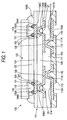
- FIG. 1 is a cross sectional view showing a related-art semiconductor device.
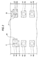
- FIG. 2 is a plan view of a related-art wiring substrate.
- a related-art semiconductor device 100 has a wiring substrate 101 and a semiconductor chip 102.
- the wiring substrate 101 has insulation layers 104, 106, and 111, a connection terminal 105, vias 107 and 112, wires 108 and 113, an external connection terminal 114, a solder resist 115, and an underfill resin 122.
- the insulation layer 104 has an opening 104A penetrating through the insulation layer 104.
- connection terminal 105 is disposed in the opening 104A.
- the widths E1 and E2 of the connection terminal 105 are configured so as to be larger than the diameter D1 of the via 107 (see, FIG. 2).
- the surface 105A of the connection terminal 105, on the side thereof to which the semiconductor chip 102 is connected, is made generally flush with the surface 104B of the insulation layer 104.
- connection terminal 105 on the side thereof to which the semiconductor chip 102 is connected, is made generally flush with the surface 104B of the insulation layer 104. This prevents solder 121 from leaking to the side surface of the connection terminal 105. This prevents a short circuit between the adjacent connection terminals 105 due to the solder 121. Therefore, it is possible to dispose the connection terminals 105 at a narrow mounting pitch.
- connection terminal 105 on the side thereof to which the semiconductor chip 102 is connected, is made generally flush with the surface 104B of the insulation layer 104. This can prevent the occurrence of voids in the underfill resin 122 disposed between the wiring substrate 101 and the semiconductor chip 102. As a result of this, it becomes possible to sufficiently ensure the connection strength between the semiconductor chip 102 and the wiring substrate 101.
- the insulation layer 106 is disposed on the surface 104C of the insulation layer 104.
- the insulation layer 106 has an opening 106A exposing the connection terminal 105.
- the via 107 is disposed in the opening 106A.
- the via 107 is connected with the connection terminal 105.
- the diameter D1 of the via 107 can be set to be, for example, 50 ⁇ m.
- the wire 108 is disposed on the surface 106B of the insulation layer 106. The wire 108 is connected with the via 107.
- the insulation layer 111 is disposed on the surface 106B of the insulation layer 106 so as to cover the via 107 and the wire 108.
- the insulation layer 111 has an opening 111A.
- the via 112 is disposed in the opening 111A.
- the via 112 is connected with the wire 108.
- the wire 113 is disposed on the surface 111B of the insulation layer 111.
- the wire 113 is connected with the via 112.
- the external connection terminal 114 is disposed on the surface 111B of the insulation layer 111.
- the external connection terminal 114 is connected with the wire 113.
- the external connection terminal 114 is electrically connected with the via 112 via the wire 113.
- the external connection terminal 114 is, for example, for establishing a connection with a mounting board such as a mother board not shown.
- the solder resist 115 is disposed on the surface 111B of the insulation layer 111 so as to cover the via 112 and the wire 113.
- the solder resist 115 has an opening 115A exposing the external connection terminal 114.
- the semiconductor chip 102 has an electrode pad 118.
- the electrode pad 118 is provided with an Au bump 119.
- the Au bump 119 is in contact with the connection terminal 105, and is fixed on the connection terminal 105 by the solder 121.
- the semiconductor chip 102 is flip-chip connected to the connection terminal 105.
- the underfill resin 122 is disposed so as to fill between the wiring substrate 101 and the semiconductor chip 102 (e.g., see Japanese Patent Unexamined Publication No. 2001-284783 )
- the widths E1 and E2 of the connection terminal 105 are required to be set larger than the diameter D1 of the via 107. Therefore, unfavorably, it is difficult to narrow the pitch of the connection terminals 105.
- Exemplary embodiments of the present invention provide a wiring substrate capable of narrowing the pitch of connection terminals, and a manufacturing method thereof, and a semiconductor device.
- a wiring substrate which includes a first insulation layer, a connection terminal disposed in the first insulation layer so as to be exposed from a first main surface of the first insulation layer, and to be electrically connected with a semiconductor chip, a second insulation layer disposed on a second main surface of the first insulation layer situated on the opposite side from the first main surface, and a via disposed in the second insulation layer, and to be electrically connected with the connection terminal, wherein the via is separated from the connection terminal, and a wiring pattern for electrically connecting the connection terminal and the via is disposed on the second main surface of the first insulation layer.
- the via is separated from the connection terminal, and the wiring pattern for electrically connecting the connection terminal and the via is disposed on the second main surface of the first insulation layer.
- a semiconductor device which includes a wiring substrate having a first insulation layer, a connection terminal disposed in the first insulation layer, and made generally flush with a first main surface of the first insulation layer, a second insulation layer disposed on a second main surface of the first insulation layer situated on the opposite side from the first main surface, and a via disposed in the second insulation layer, a semiconductor chip flip-chip connected to the connection terminal, and an underfill resin disposed between the semiconductor chip and the wiring substrate, wherein the via is separated from the connection terminal, and a wiring pattern for electrically connecting the connection terminal and the via is disposed on the second main surface of the first insulation layer.
- the via is separated from the connection terminal, and the wiring pattern for electrically connecting the connection terminal and the via is disposed on the second main surface of the first insulation layer.
- a method for manufacturing a wiring substrate including a first insulation layer, a plurality of connection terminals disposed on the first insulation layer, and made generally flush with a first main surface of the first insulation layer, a wiring pattern disposed on a second main surface of the first insulation layer situated on the opposite side from the first main surface, and connected to the connection terminals, a second insulation layer disposed on the second main surface of the first insulation layer, and covering the wiring pattern, and a via disposed in the second insulation layer, and connected to the wiring pattern, characterized by including: a first insulation layer formation step of forming the first insulation layer on a metal plate serving as a support substrate, an opening formation step of forming an opening capable of mounting at least two or more of the connection terminals on the first insulation layer, and a connection terminal formation step of forming the connection terminals in the opening.
- the method includes an opening formation step of forming an opening capable of mounting at least two or more of the connection terminals on the first insulation layer. As a result, it is possible to form connection terminals arranged at a narrow pitch.
- FIG. 3 is a plan view of a semiconductor device in accordance with a first embodiment of the present invention.
- a semiconductor device 10 of the first embodiment has a wiring substrate 11 and a semiconductor chip 12.
- the wiring substrate 11 has an insulation layer 14 which is a first insulation layer, a connection terminal 15, a wiring pattern 16, an insulation layer 21 which is a second insulation layer, vias 24 and 31, a via connection part 25, an insulation layer 27, an external connection terminal 32, and a solder resist 34.
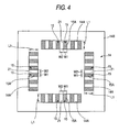
- FIG. 4 is a plan view of the wiring substrate shown in FIG. 3.
- the insulation layer 14 has an opening 14A penetrating through the insulation layer 14.
- the opening 14A is formed in such a shape as to be capable of mounting at least two or more connection terminals 15.
- a thermosetting resin or a photosensitive resin can be used as the insulation layer 14.
- the thickness M1 of the insulation layer 14 can be set to be, for example, 5 ⁇ m to 10 ⁇ m.
- the opening 14A is formed in a shape having such a size as to be capable of mounting at least two or more connection terminals 15. As a result, it is possible to form the opening 14A in the insulation layer 14 with ease.
- connection terminal 15 is mounted in the opening 14A.
- An Au bump 37 disposed on the semiconductor chip 12 is in contact with the surface 15A of the connection terminal 15.
- solder 38 for connecting the Au bump 37 to the connection terminal 15 is disposed on the surface 15A of the connection terminal 15.
- the surface 15A of the connection terminal 15 is made generally flush with the top side 14B of the first insulation layer 14.
- the width W1 of the connection terminal 15 can be set to be, for example, 20 ⁇ m.
- the mounting pitch W2 of the connection terminals 15 can be set to be, for example, 20 ⁇ m.
- the length L1 of the connection terminal 15 can be set to be, for example, 500 ⁇ m.
- connection terminal 15A of the connection terminal 15, on the side thereof to which the semiconductor chip 12 is connected is made generally flush with the top side 14B of the insulation layer 14. This prevents solder 38 from leaking to the side surface of the connection terminal 15. This prevents a short circuit between the adjacent connection terminals 15 due to the solder 38. Therefore, it is possible to dispose the connection terminals 15 at a narrow mounting pitch.
- connection terminal 15A of the connection terminal 15, on the side thereof to which the semiconductor chip 12 is connected is made generally flush with the surface 14B of the insulation layer 14. As a result of this, it becomes possible to sufficiently ensure the clearance between the wiring substrate 11 and the semiconductor chip 12. This can prevent the occurrence of voids in an underfill resin 39 filling between the wiring substrate 11 and the semiconductor chip 12.
- the wiring pattern 16 has a wiring part 17 and a via connection part 18.
- the wiring part 17 is disposed on the surface 14C of the insulation layer 14.
- the wiring part 17 is connected with the connection terminal 15.
- the connection part 17 is for establishing an electrical connection between the connection terminal 15 and the via connection part 18.
- Provision of such a wiring part 17 can dispose the via connection part 18 to be electrically connected with the connection terminal 15 at a prescribed position.
- connection terminal 15 and the wiring pattern 16 described above are integrally formed such that the wiring pattern 16 extends from the connection terminal 15 over from the opening 14A portion to the surface 14C of the insulation layer 14.
- the via connection part 18 is disposed on the surface 14C of the insulation layer 14.
- the via connection part 18 is separated from the connection terminal 15. Further, the via connection part 18 is formed in a shape larger in width than the connection terminal 15.
- the via connection part 18 is connected with the wiring part 17.
- the via connection part 18 is electrically connected with the connection terminal 15 via the wiring part 17. To the via connection part 18, the via 24 is connected.
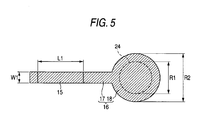
- FIG. 5 is a plan view of the connection terminal and the wiring pattern shown in FIG. 3.
- the via connection part 18 is circular in plan configuration.
- the via connection part 18 is formed in a shape larger in width than the diameter R1 of the via 24.
- the diameter R2 of the via connection part 18 can be set to be, for example, 130 ⁇ m.
- the wiring pattern 16 including the wiring part 17 for establishing an electrical connection between the connection terminal 15 and the via connection part 18, and the via connection part 18 formed in a shape larger in width than the diameter R1 of the via 24 is disposed on the surface 14C of the insulation layer 14. This eliminates the necessity of establishing a direct connection between the connection terminal 15 and the via 24. As a result of this, it becomes possible to make small the width W1 and the mounting pitch W2 of the connection terminals 15. As a result, it is possible to mount the connection terminals 15 at a narrow pitch.
- the insulation layer 21 is disposed on the surface 14C of the insulation layer 14 in such a manner as to cover the connection terminal 15, the via connection part 18, and the wiring part 17.
- the insulation layer 21 has an opening 21A exposing a part of the via connection part 18.
- a thermosetting resin or a photosensitive resin can be used as the insulation layer 21 .
- the via 24 is disposed in the opening 21A.
- the via 24 is connected with the via connection part 18.
- the via connection part 25 is disposed on the surface 21C of the insulation layer 21.
- the via connection part 25 is connected with the via 24.
- the insulation layer 27 is disposed on the surface 21C of the insulation layer 21 in such a manner as to cover the via 24 and a part of the via connection part 25.
- the insulation layer 27 has an opening 27A exposing a part of the via connection part 25.
- a thermosetting resin or a photosensitive resin can be used as the insulation layer 27 .
- the via 31 is disposed in the opening 27A.
- the via 31 is connected with the via connection part 25.
- the external connection terminal 32 is disposed on the surface 27B of the insulation layer 27.
- the external connection terminal 32 is for establishing a connection with a mounting board such as a mother board.
- the solder resist 34 is disposed on the surface 27B of the insulation layer 27 in such a manner as to cover the via 31.
- the semiconductor chip 12 has an electrode pad 36.
- the electrode pad 36 is provided with an Au bump 37.
- the Au bump 37 is in contact with the top surface 15A of the connection terminal 15.
- the Au bump 37 is electrically connected with the connection terminal 15.
- the periphery of the Au bump 37 is covered with the solder 38 disposed on the top surface 15A of the connection terminal 15.
- the semiconductor chip 12 is flip-chip connected to the connection terminal 15.
- the underfill resin 39 is disposed so as to fill between the wiring substrate 11 and the semiconductor chip 12.
- the underfill resin 39 is for improving the connection strength between the semiconductor chip 12 and the wiring substrate 11, and for reducing the stress caused by the difference in thermal expansion between the semiconductor chip 12 and the wiring substrate 11.
- the wiring pattern 16 including the wiring part 17 for establishing an electrical connection between the connection terminal 15 and the via connection part 18, and the via connection part 18 formed in a shape larger in width than the diameter R1 of the via 24 is disposed on the surface 14C of the insulation layer 14. This eliminates the necessity of establishing a direct connection between the connection terminal 15 and the via 24. As a result of this, it is possible to make small the width W1 and the mounting pitch W2 of the connection terminals 15, and to mount the connection terminals 15 at a narrow pitch.
- connection terminal 15A of the connection terminal 15, on the side thereof to which the semiconductor chip 12 is connected is made generally flush with the surface 14B of the insulation layer 14.
- the solder 38 will not leak to the side surface of the connection terminal 15 .
- the surface 15A of the connection terminal 15, on the side thereof to which the semiconductor chip 12 is connected is made generally flush with the surface 14B of the insulation layer 14. As a result of this, it becomes possible to sufficiently ensure the clearance between the wiring substrate 11 and the semiconductor chip 12. This can prevent the occurrence of voids in the underfill resin 39 filling between the wiring substrate 11 and the semiconductor chip 12.
- FIGS. 6 to 17 are views each showing a manufacturing step of the wiring substrate in accordance with the first embodiment of the present invention.
- FIG. 18 is a plan view of a structure shown in FIG. 7.
- FIG. 19 is a plan view of a structure shown in FIG. 9.
- FIG. 20 is a plan view of a structure shown in FIG. 12.
- the same constitutional components as those of the wiring substrate 11 described previously are given the same reference numerals and signs.
- the insulation layer 14 is formed on a metal plate 43 serving as a support plate (first insulation layer formation step) .
- a metal plate 43 for example, a Cu plate can be used.
- a thickness M2 of the metal plate 43 can be set to be, for example, 50 ⁇ m to 200 ⁇ m.
- metal foil e.g., Cu foil
- a sheet of the metal plate 43 has a plurality of wiring substrate formation regions in which the wiring substrate 11 is formed. A plurality of the wiring substrates 11 are simultaneously formed in a sheet of the metal plate 43. A plurality of the wiring substrate formation regions are arranged in a grid.
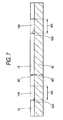
- the insulation layer 14 for example, a thermosetting resin or a photosensitive resin can be used.
- a solder resist can be used as the insulation layer 14.
- the insulation layer 14 can be formed by a printing method.
- the thickness M1 of the insulation layer 14 can be set to be, for example, 5 ⁇ m to 10 ⁇ m.
- an opening 14A capable of mounting at least two or more connection terminals 15 is formed in the insulation layer 14 (opening formation step).
- the opening 14A is formed so as to expose the top surface 43A of the metal plate 43.
- the opening 14A is formed by using, for example, laser.
- the opening 14A is formed by photolithography.
- the opening 14A is an opening having a large opening area.
- the width W3 of the opening 14A can be set to be, for example, 500 ⁇ m.
- the length L3 of the opening 14A can be set to be, for example, 3 mm.
- the opening 14A configured to have a size capable of mounting at least two or more connection terminals 15 is formed. As a result, it is possible to form the opening 14A more easily as compared with the case where an opening with a size corresponding to that of one connection terminal 15 is formed.
- a seed layer 45 is formed in such a manner as to cover the top surface side of the structure shown in FIG. 7.
- a resist film 46 having openings 46A is formed on the seed layer 45.
- the seed layer 45 can be formed by, for example, a sputtering method or an electroless plating method.
- a Cu layer can be used as the seed layer 45.
- the openings 46A are formed so as to expose the portions of the seed layer 45 corresponding to the formation region of the connection terminals 15 and the wiring pattern 16.
- a plating film 47 is formed on the seed layer 45 exposed at the openings 46A.
- a plating film 47 for example, a Cu plating film can be used (for a plan view of the structure shown in FIG. 9, see, FIG. 19).
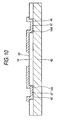
- the resist film 46 is removed.
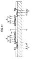
- connection terminal formation step unnecessary portions of the seed layer 45 not covered with the plating film 47 are removed.
- connection terminals 15 and the wiring pattern 16 including the wiring part 17 and the via connection part 18 are simultaneously formed (connection terminal formation step).
- the connection terminal 15 and the wiring pattern 16 are formed of the seed layer 45 and the plating film 47.
- the connection terminal 15 and the wiring pattern 16 are integrally formed such that the wiring pattern 16 extends from the connection terminal 15 over from the opening 14A portion to the surface 14C of the insulation layer 14.
- the insulation layer 21 having openings 21A is formed on the structure shown in FIG. 11 (for the plan view of the structure shown in FIG. 12, see, FIG. 20).
- the diameter R3 of the opening 21A is smaller than the diameter R2 of the via connection part 18.
- the diameter R3 of the opening 21A can be set to be, for example, 50 ⁇ m.
- the opening 21A is formed by, for example, laser.
- the opening 21A is formed by photolithography.
- the diameter R3 of the opening 21A is 50 ⁇ m
- the diameter R2 of the via connection part 18 can be set to be, for example, 130 ⁇ m.
- the via 24 and the via connection part 25 are simultaneously formed with the same procedure as the steps shown in FIGS. 8 to 11 described previously.
- the via 24 and the via connection part 25 are formed of the seed layer and the plating film.
- the diameter R1 of the via 24 is generally equal to the diameter R3 of the opening 21A.
- the diameter R1 of the via 24 can be set to be, for example, 50 ⁇ m.
- the insulation layer 27 having openings 27A is formed on the structure shown in FIG. 13.
- a thermosetting resin or a photosensitive resin can be used as the insulation layer 27 for example.
- the insulation layer 27 having the openings 27A can be formed with the same procedure as the steps shown in FIG. 12 described previously.
- the via 31 and the external connection terminal 32 are simultaneously formed with the same procedure as the steps shown in FIGS. 8 to 11 described previously.
- the via 31 and the external connection terminal 32 are formed of the seed layer and the plating film.
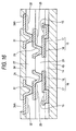
- the solder resist 34 having the openings 34A is formed in such a manner as to cover the top surface side of the structure shown in FIG. 15.
- the opening 34A is formed in such a manner as to expose the external connection terminal 32.
- the metal plate 43 which is a support plate is removed (metal plate removing step). Then, the insulation layers 14, 21, and 27 situated between the wiring substrate formation regions are cut, so that the wiring substrate 11 is formed into individual pieces. As a result, a plurality of wiring substrates 11 are manufactured. Incidentally, in FIG. 17, only one wiring substrate 11 is shown.
- the metal plate 43 can be removed by wet etching. At this step, the metal plate 43 may be removed in such a manner that the metal plate 43 is left in a frame-like configuration around the chip mounting part.
- the opening 14A capable of mounting at least two or more connection terminals 15 is formed in the insulation layer 14.
- the opening 14A it is possible to form the opening 14A more easily as compared with the case where openings each in a small shape corresponding to the shape of one connection terminal 15 is formed in the insulation layer 14. This can reduce the manufacturing cost of the wiring substrate 11.
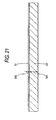
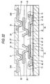
- FIGS. 21 to 24 are each a view showing a manufacturing step of the wiring substrate in accordance with a modified example of the first embodiment of the present invention.
- a metal layer 51 is formed on the metal plate 43 serving as the support plate.
- the metal layer 51 is formed of a metal which is resistant to etching by the etchant for use in removing the metal plate 43.
- the metal forming the metal plate 43, the seed layer 45, and the plating film 47 is Cu, as the material for the metal layer 51, for example, Ni can be used.
- the thickness M3 of the metal layer 51 can be set to be, for example, 5 ⁇ m.
- a structure corresponding to the wiring substrate 11 is formed on the metal layer 51 with the same procedure as the steps shown in FIGS. 6 to 16 described previously.
- the metal plate 43 is removed by wet etching.
- the etchant for use in wet etching the one with which the metal layer 51 is resistant to etching (the one against which the metal layer 51 serves as an etching stopper) is used.
- the metal layer 51 which is resistant to etching with the etchant for removing the metal plate 43 is formed between the metal plate 43 and the connection terminal 15. This can prevent the connection terminal 15 from being etched for removing the metal plate 43.
- the metal layer 51 is removed by wet etching. As a result of this, the wiring substrate 11 is manufactured.
- the etchant for removing the metal layer 51 the one with which the connection terminal 51 is resistant to etching is used.
- the metal layer 51 is removed by using the etchant with which the connection terminal 15 is resistant to etching. This can prevent the connection terminal 15 from being etched by the etchant.
- the metal layer 51 which is resistant to etching with the etchant for use in removing the metal plate 43 is formed between the metal plate 43 and the connection terminal 15. This can prevent the connection terminal 15 from being etched in the removing step of the metal plate 43.
- the metal layer 51 is removed by using the etchant with which the connection terminal 15 is resistant to etching. This can prevent the connection terminal 15 from being etched for etching the metal layer 51.
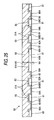
- FIG. 25 is a cross sectional view of a wiring substrate in accordance with a second embodiment of the present invention.
- FIG. 26 is a plan view of a wiring substrate in accordance with the second embodiment of the present invention.
- a wiring substrate 60 of the second embodiment has insulation layers 61 and 68, a connection terminal 62, wires 63 and 65, and external connection terminals 64 and 66.
- the insulation layer 61 has openings 69A to 69C.
- the opening 69A is formed in such a shape as to be capable of mounting at least two or more connection terminals 62.
- the openings 69B are disposed outside the opening 69A, and a plurality of the openings 69B are formed in such a manner as to surround the formation region of the opening 69A.
- the openings 69C are arranged outside the opening 69B, and a plurality of the openings 69C are formed in such a manner as to surround the openings 69B.
- a thermosetting resin or a photosensitive resin can be used as the insulation layer 61.
- the thickness M4 of the insulation layer 61 can be set to be, for example, 5 ⁇ m to 10 ⁇ m.
- connection terminal 62 is mounted in the opening 69A. To the surface 62A of the connection terminal 62, a semiconductor chip not shown is connected. The surface 62A of the connection terminal 62 is made generally flush with the surface 61B of the insulation layer 61.
- the width W4 of the connection terminal 62 can be set to be, for example, 20 ⁇ m.
- the mounting pitch W5 of the connection terminal 62 can be set to be, for example, 20 ⁇ m.
- the length L2 of the connection terminal 62 can be set to be, for example, 500 ⁇ m.
- connection terminal 62 on the side thereof to which the semiconductor chip is connected, is made generally flush with the surface 61B of the insulation layer 61.
- solder will not leak to the side surface of the connection terminal 62. This prevents a short circuit between the adjacent connection terminals 62 due to the solder. Therefore, it is possible to dispose the connection terminals 62 at a narrow mounting pitch.
- connection terminal 62 on the side thereof to which the semiconductor chip is connected, is made generally flush with the surface 61B of the insulation layer 61.
- the semiconductor chip is flip-flop connected to the connection terminal 62, it becomes possible to ensure a sufficient clearance between the wiring substrate 60 and the semiconductor chip. Accordingly, it is possible to prevent the occurrence of voids in the underfill resin filling between the wiring substrate 60 and the semiconductor chip.
- a wire 63 is disposed on the surface 61A of the insulation layer 61.
- the one edge of the wire 63 is connected to the connection terminal 62, and the other edge thereof is electrically connected to an external connection terminal 64.
- the external connection terminal 64 is disposed in the opening 69B.
- the external connection terminal 64 is for establishing an electrical connection with a mounting board such as a mother board.
- the external connection terminal 64 is electrically connected with the connection terminal 62 via the wire 63.
- the surface 64A of the external connection terminal 64 is made generally flush with the surface 61B of the insulation layer 61. In other words, the external connection terminal 64 is disposed on the same plane as that of the connection terminal 62.
- a wire 65 is disposed on the surface 61A of the insulation layer 61.
- the one edge of the wire 65 is connected to the connection terminal 62, and the other edge thereof is electrically connected to an external connection terminal 66.
- the external connection terminal 66 is disposed in the opening 69C.
- the external connection terminal 66 is for establishing an electrical connection with a mounting board such as a mother board.
- the external connection terminal 66 is electrically connected with the connection terminal 62 via the wire 65.
- the surface 66A of the external connection terminal 66 is made generally flush with the surface 61B of the insulation layer 61. In other words, the external connection terminal 66 is disposed on the same plane as that of the connection terminal 62.
- connection terminal 62 and the external connection terminals 64 and 66 are disposed on the same plane.
- connection terminal 62 and the external connection terminal 64 are electrically connected by the wire 63 disposed on the surface 61A of the insulation layer 61.
- connection terminal 62 and the external connection terminal 66 are electrically connected by the wire 65 disposed on the surface 61A of the insulation layer 61.
- the via for establishing an electrical connection between the external connection terminals 64 and 66 and the connection terminal 62 becomes unnecessary.
- connection terminal 62 is made generally flush with the surface 61B of the insulation layer 61.
- solder will not leak to the side surface of the connection terminal 62. This prevents a short circuit between the adjacent connection terminals 62 due to the solder. Therefore, it is possible to dispose the connection terminals 62 at a narrow mounting pitch.
- connection terminal 62 on the side thereof to which the semiconductor chip is connected, is made generally flush with the surface 61B of the insulation layer 61.
- the semiconductor chip is flip-flop connected to the connection terminal 62, it becomes possible to ensure a sufficient clearance between the wiring substrate 60 and the semiconductor chip. Accordingly, it is possible to prevent the occurrence of voids in the underfill resin filling between the wiring substrate 60 and the semiconductor chip.
- the insulation layer 68 is disposed on the surface 61A side of the insulation layer 61 in such a manner as to cover the connection terminals 62, the wires 63 and 65, and the external connection terminals 64 and 66.
- the insulation layer 68 performs a function of a reinforcing plate for reinforcing the strength of the wiring substrate 60.
- a resin containing a reinforcing material such as glass cloth may be used.
- a prepreg resin can be used as the insulation layer 68.
- the thickness M5 of the insulation layer 68 can be set to be, for example, 50 ⁇ m to 200 ⁇ m.
- connection terminals 62 and the external connection terminals 64 and 66 are disposed on the same plane.
- connection terminal 62 and the external connection terminal 64 are electrically connected by the wire 63 disposed on the surface 61A of the insulation layer 61.
- connection terminal 62 and the external connection terminal 66 are electrically connected by the wire 65 disposed on the surface 61A of the insulation layer 61.
- the via for establishing an electrical connection between the external connection terminals 64 and 66 and the connection terminal 62 becomes unnecessary.
- FIG. 27 is a cross sectional view of a semiconductor device in accordance with the second embodiment of the present invention.
- the same constitutional elements as those of the semiconductor device 10 of the first embodiment are given the same reference numerals and signs.
- a semiconductor device 75 of the second embodiment has a wiring substrate 60, a semiconductor chip 12, and solder balls 76 and 77.
- the semiconductor chip 12 is flip-chip connected to the connection terminal 62.
- the solder ball 76 is disposed on an external connection terminal 64.
- the solder ball 77 is disposed on an external connection terminal 66.
- the external connection terminals 64 and 66 are electrically connected with a mother board not shown via the solder balls 76 and 77, respectively.
- the present invention is applicable to a wiring substrate including a connection terminal to be electrically connected with a semiconductor chip, and a manufacturing method thereof, and a semiconductor device.
Landscapes
- Engineering & Computer Science (AREA)
- Manufacturing & Machinery (AREA)
- Microelectronics & Electronic Packaging (AREA)
- Production Of Multi-Layered Print Wiring Board (AREA)
- Internal Circuitry In Semiconductor Integrated Circuit Devices (AREA)
Abstract
Description
- This application claims priority to
Japanese Patent Application No. 2006-209845, filed August 1, 2006 - The present disclosure relates to a wiring substrate and a manufacturing method thereof, and a semiconductor device. More particularly, it relates to a wiring substrate including a connection terminal to be connected with a semiconductor chip, and a manufacturing method thereof, and a semiconductor device.
- The mounting pitch of connection terminals to be disposed on a wiring substrate has been narrowed (which is hereinafter referred to as "narrowing of pitch") due to recent miniaturization of a semiconductor chip. As the semiconductor device including a wiring substrate having connection terminals narrowed in pitch, for example, there is the one as shown in FIG. 1.
- FIG. 1 is a cross sectional view showing a related-art semiconductor device. FIG. 2 is a plan view of a related-art wiring substrate.
- By reference to FIG. 1, a related-
art semiconductor device 100 has awiring substrate 101 and asemiconductor chip 102. Thewiring substrate 101 hasinsulation layers connection terminal 105,vias wires external connection terminal 114, a solder resist 115, and anunderfill resin 122. Theinsulation layer 104 has an opening 104A penetrating through theinsulation layer 104. - The
connection terminal 105 is disposed in the opening 104A. The widths E1 and E2 of theconnection terminal 105 are configured so as to be larger than the diameter D1 of the via 107 (see, FIG. 2). Thesurface 105A of theconnection terminal 105, on the side thereof to which thesemiconductor chip 102 is connected, is made generally flush with thesurface 104B of theinsulation layer 104. - Thus, the
surface 105A of theconnection terminal 105, on the side thereof to which thesemiconductor chip 102 is connected, is made generally flush with thesurface 104B of theinsulation layer 104. This preventssolder 121 from leaking to the side surface of theconnection terminal 105. This prevents a short circuit between theadjacent connection terminals 105 due to thesolder 121. Therefore, it is possible to dispose theconnection terminals 105 at a narrow mounting pitch. - Further, the
surface 105A of theconnection terminal 105, on the side thereof to which thesemiconductor chip 102 is connected, is made generally flush with thesurface 104B of theinsulation layer 104. This can prevent the occurrence of voids in theunderfill resin 122 disposed between thewiring substrate 101 and thesemiconductor chip 102. As a result of this, it becomes possible to sufficiently ensure the connection strength between thesemiconductor chip 102 and thewiring substrate 101. - The
insulation layer 106 is disposed on thesurface 104C of theinsulation layer 104. Theinsulation layer 106 has an opening 106A exposing theconnection terminal 105. Thevia 107 is disposed in the opening 106A. Thevia 107 is connected with theconnection terminal 105. The diameter D1 of thevia 107 can be set to be, for example, 50 µm. Thewire 108 is disposed on thesurface 106B of theinsulation layer 106. Thewire 108 is connected with thevia 107. - The
insulation layer 111 is disposed on thesurface 106B of theinsulation layer 106 so as to cover thevia 107 and thewire 108. Theinsulation layer 111 has an opening 111A. Thevia 112 is disposed in the opening 111A. Thevia 112 is connected with thewire 108. - The
wire 113 is disposed on thesurface 111B of theinsulation layer 111. Thewire 113 is connected with thevia 112. Theexternal connection terminal 114 is disposed on thesurface 111B of theinsulation layer 111. Theexternal connection terminal 114 is connected with thewire 113. Theexternal connection terminal 114 is electrically connected with thevia 112 via thewire 113. Theexternal connection terminal 114 is, for example, for establishing a connection with a mounting board such as a mother board not shown. Thesolder resist 115 is disposed on thesurface 111B of theinsulation layer 111 so as to cover thevia 112 and thewire 113. Thesolder resist 115 has an opening 115A exposing theexternal connection terminal 114. - The
semiconductor chip 102 has anelectrode pad 118. Theelectrode pad 118 is provided with anAu bump 119. TheAu bump 119 is in contact with theconnection terminal 105, and is fixed on theconnection terminal 105 by thesolder 121. Thesemiconductor chip 102 is flip-chip connected to theconnection terminal 105. - The
underfill resin 122 is disposed so as to fill between thewiring substrate 101 and the semiconductor chip 102 (e.g., seeJapanese Patent Unexamined Publication No. 2001-284783 - However, with the related-
art wiring substrate 101, the widths E1 and E2 of theconnection terminal 105 are required to be set larger than the diameter D1 of thevia 107. Therefore, unfavorably, it is difficult to narrow the pitch of theconnection terminals 105. - Exemplary embodiments of the present invention provide a wiring substrate capable of narrowing the pitch of connection terminals, and a manufacturing method thereof, and a semiconductor device.
- In accordance with one viewpoint of the present invention, there is provided a wiring substrate, which includes a first insulation layer, a connection terminal disposed in the first insulation layer so as to be exposed from a first main surface of the first insulation layer, and to be electrically connected with a semiconductor chip, a second insulation layer disposed on a second main surface of the first insulation layer situated on the opposite side from the first main surface, and a via disposed in the second insulation layer, and to be electrically connected with the connection terminal, wherein the via is separated from the connection terminal, and a wiring pattern for electrically connecting the connection terminal and the via is disposed on the second main surface of the first insulation layer.
- In accordance with the present invention, the via is separated from the connection terminal, and the wiring pattern for electrically connecting the connection terminal and the via is disposed on the second main surface of the first insulation layer. As a result, it becomes possible to make the width of the connection terminal smaller than the diameter of the via. Therefore, it is possible to narrow the pitch of the connection terminals.
- In accordance with another aspect of the present invention, there is provided a semiconductor device, which includes a wiring substrate having a first insulation layer, a connection terminal disposed in the first insulation layer, and made generally flush with a first main surface of the first insulation layer, a second insulation layer disposed on a second main surface of the first insulation layer situated on the opposite side from the first main surface, and a via disposed in the second insulation layer, a semiconductor chip flip-chip connected to the connection terminal, and an underfill resin disposed between the semiconductor chip and the wiring substrate, wherein the via is separated from the connection terminal, and a wiring pattern for electrically connecting the connection terminal and the via is disposed on the second main surface of the first insulation layer.
- In accordance with the present invention, the via is separated from the connection terminal, and the wiring pattern for electrically connecting the connection terminal and the via is disposed on the second main surface of the first insulation layer. As a result, it becomes possible to make the width of the connection terminal smaller than the diameter of the via. Therefore, it is possible to narrow the pitch of the connection terminals.
- In accordance with a still other aspect of the present invention, there is provided a method for manufacturing a wiring substrate including a first insulation layer, a plurality of connection terminals disposed on the first insulation layer, and made generally flush with a first main surface of the first insulation layer, a wiring pattern disposed on a second main surface of the first insulation layer situated on the opposite side from the first main surface, and connected to the connection terminals, a second insulation layer disposed on the second main surface of the first insulation layer, and covering the wiring pattern, and a via disposed in the second insulation layer, and connected to the wiring pattern, characterized by including: a first insulation layer formation step of forming the first insulation layer on a metal plate serving as a support substrate, an opening formation step of forming an opening capable of mounting at least two or more of the connection terminals on the first insulation layer, and a connection terminal formation step of forming the connection terminals in the opening.
- In accordance with the present invention, the method includes an opening formation step of forming an opening capable of mounting at least two or more of the connection terminals on the first insulation layer. As a result, it is possible to form connection terminals arranged at a narrow pitch.
- In accordance with the present invention, it is possible to narrow the pitch of connection terminals.
Other features and advantages may be apparent from the following detailed description, the accompanying drawings and the claims. -
- FIG. 1 is a cross sectional view showing a related-art semiconductor device;
- FIG. 2 is a plan view of a related-art wiring substrate;
- FIG. 3 is a plan view of a semiconductor device in accordance with a first embodiment of the present invention;
- FIG. 4 is a plan view of a wiring substrate shown in FIG. 3;
- FIG. 5 is a plan view of a connection terminal and a wiring pattern shown FIG. 3;
- FIG. 6 is a view (first) showing a manufacturing step of the wiring substrate in accordance with the first embodiment of the present invention;
- FIG. 7 is a view (second) showing a manufacturing step of the wiring substrate in accordance with the first embodiment of the present invention;
- FIG. 8 is a view (third) showing a manufacturing step of the wiring substrate in accordance with the first embodiment of the present invention;
- FIG. 9 is a view (fourth) showing a manufacturing step of the wiring substrate in accordance with the first embodiment of the present invention;
- FIG. 10 is a view (fifth) showing a manufacturing step of the wiring substrate in accordance with the first embodiment of the present invention;
- FIG. 11 is a view (sixth) showing a manufacturing step of the wiring substrate in accordance with the first embodiment of the present invention;
- FIG. 12 is a view (seventh) showing a manufacturing step of the wiring substrate in accordance with the first embodiment of the present invention;
- FIG. 13 is a view (eighth) showing a manufacturing step of the wiring substrate in accordance with the first embodiment of the present invention;
- FIG. 14 is a view (ninth) showing a manufacturing step of the wiring substrate in accordance with the first embodiment of the present invention;
- FIG. 15 is a view (tenth) showing a manufacturing step of the wiring substrate in accordance with the first embodiment of the present invention;
- FIG. 16 is a view (eleventh) showing a manufacturing step of the wiring substrate in accordance with the first embodiment of the present invention;
- FIG. 17 is a view (twelfth) showing a manufacturing step of the wiring substrate in accordance with the first embodiment of the present invention;
- FIG. 18 is a plan view of the structure shown in FIG. 7;
- FIG. 19 is a plan view of the structure shown in FIG. 9;
- FIG. 20 is a plan view of the structure shown in FIG. 12;
- FIG. 21 is a view (first) showing a manufacturing step of a wiring substrate in accordance with a modified example of the first embodiment of the present invention;
- FIG. 22 is a view (second) showing a manufacturing step of the wiring substrate in accordance with the modified example of the first embodiment of the present invention;
- FIG. 23 is a view (third) showing a manufacturing step of the wiring substrate in accordance with the modified example of the first embodiment of the present invention;
- FIG. 24 is a view (fourth) showing a manufacturing step of the wiring substrate in accordance with the modified example of the first embodiment of the present invention;
- FIG. 25 is a cross sectional view showing a wiring substrate in accordance with a second embodiment of the present invention;
- FIG. 26 is a plan view of the wiring substrate in accordance with the second embodiment of the present invention; and
- FIG. 27 is a cross sectional view of a semiconductor device in accordance with the second embodiment of the present invention.
- Then, the present invention will be described by way of embodiments by reference to the accompanying drawings.
- FIG. 3 is a plan view of a semiconductor device in accordance with a first embodiment of the present invention.
By reference to FIG. 3, asemiconductor device 10 of the first embodiment has awiring substrate 11 and asemiconductor chip 12. Thewiring substrate 11 has aninsulation layer 14 which is a first insulation layer, aconnection terminal 15, awiring pattern 16, aninsulation layer 21 which is a second insulation layer, vias 24 and 31, a viaconnection part 25, aninsulation layer 27, anexternal connection terminal 32, and a solder resist 34. - FIG. 4 is a plan view of the wiring substrate shown in FIG. 3.
- The
insulation layer 14 has anopening 14A penetrating through theinsulation layer 14. By reference to FIG. 4, theopening 14A is formed in such a shape as to be capable of mounting at least two ormore connection terminals 15. As theinsulation layer 14, a thermosetting resin or a photosensitive resin can be used. The thickness M1 of theinsulation layer 14 can be set to be, for example, 5 µm to 10 µm. - Thus, the
opening 14A is formed in a shape having such a size as to be capable of mounting at least two ormore connection terminals 15. As a result, it is possible to form theopening 14A in theinsulation layer 14 with ease. - By reference to FIGS. 3 and 4, the
connection terminal 15 is mounted in theopening 14A. An Au bump 37 disposed on thesemiconductor chip 12 is in contact with thesurface 15A of theconnection terminal 15. On thesurface 15A of theconnection terminal 15,solder 38 for connecting theAu bump 37 to theconnection terminal 15 is disposed. Thesurface 15A of theconnection terminal 15 is made generally flush with thetop side 14B of thefirst insulation layer 14. The width W1 of theconnection terminal 15 can be set to be, for example, 20 µm. Whereas, the mounting pitch W2 of theconnection terminals 15 can be set to be, for example, 20 µm. The length L1 of theconnection terminal 15 can be set to be, for example, 500 µm. - Thus, the
surface 15A of theconnection terminal 15, on the side thereof to which thesemiconductor chip 12 is connected, is made generally flush with thetop side 14B of theinsulation layer 14. This preventssolder 38 from leaking to the side surface of theconnection terminal 15. This prevents a short circuit between theadjacent connection terminals 15 due to thesolder 38. Therefore, it is possible to dispose theconnection terminals 15 at a narrow mounting pitch. - Further, the
surface 15A of theconnection terminal 15, on the side thereof to which thesemiconductor chip 12 is connected, is made generally flush with thesurface 14B of theinsulation layer 14. As a result of this, it becomes possible to sufficiently ensure the clearance between thewiring substrate 11 and thesemiconductor chip 12. This can prevent the occurrence of voids in anunderfill resin 39 filling between thewiring substrate 11 and thesemiconductor chip 12. - The
wiring pattern 16 has awiring part 17 and a viaconnection part 18. Thewiring part 17 is disposed on thesurface 14C of theinsulation layer 14. Thewiring part 17 is connected with theconnection terminal 15. Theconnection part 17 is for establishing an electrical connection between theconnection terminal 15 and the viaconnection part 18. - Provision of such a
wiring part 17 can dispose the viaconnection part 18 to be electrically connected with theconnection terminal 15 at a prescribed position. - The
connection terminal 15 and thewiring pattern 16 described above are integrally formed such that thewiring pattern 16 extends from theconnection terminal 15 over from theopening 14A portion to thesurface 14C of theinsulation layer 14. - The via
connection part 18 is disposed on thesurface 14C of theinsulation layer 14. The viaconnection part 18 is separated from theconnection terminal 15. Further, the viaconnection part 18 is formed in a shape larger in width than theconnection terminal 15. The viaconnection part 18 is connected with thewiring part 17. The viaconnection part 18 is electrically connected with theconnection terminal 15 via thewiring part 17. To the viaconnection part 18, the via 24 is connected. - FIG. 5 is a plan view of the connection terminal and the wiring pattern shown in FIG. 3.
- By reference to FIG. 5, the via
connection part 18 is circular in plan configuration. The viaconnection part 18 is formed in a shape larger in width than the diameter R1 of the via 24. When the diameter R1 of the via 24 is 50 µm, the diameter R2 of the viaconnection part 18 can be set to be, for example, 130 µm. - Thus, the
wiring pattern 16 including thewiring part 17 for establishing an electrical connection between theconnection terminal 15 and the viaconnection part 18, and the viaconnection part 18 formed in a shape larger in width than the diameter R1 of the via 24 is disposed on thesurface 14C of theinsulation layer 14. This eliminates the necessity of establishing a direct connection between theconnection terminal 15 and the via 24. As a result of this, it becomes possible to make small the width W1 and the mounting pitch W2 of theconnection terminals 15. As a result, it is possible to mount theconnection terminals 15 at a narrow pitch. - By reference to FIG. 3, the
insulation layer 21 is disposed on thesurface 14C of theinsulation layer 14 in such a manner as to cover theconnection terminal 15, the viaconnection part 18, and thewiring part 17. Theinsulation layer 21 has anopening 21A exposing a part of the viaconnection part 18. As theinsulation layer 21, a thermosetting resin or a photosensitive resin can be used. - The via 24 is disposed in the
opening 21A. The via 24 is connected with the viaconnection part 18. The viaconnection part 25 is disposed on thesurface 21C of theinsulation layer 21. The viaconnection part 25 is connected with the via 24. - The
insulation layer 27 is disposed on thesurface 21C of theinsulation layer 21 in such a manner as to cover the via 24 and a part of the viaconnection part 25. Theinsulation layer 27 has anopening 27A exposing a part of the viaconnection part 25. As theinsulation layer 27, a thermosetting resin or a photosensitive resin can be used. - The via 31 is disposed in the
opening 27A. The via 31 is connected with the viaconnection part 25. Theexternal connection terminal 32 is disposed on thesurface 27B of theinsulation layer 27. Theexternal connection terminal 32 is for establishing a connection with a mounting board such as a mother board. The solder resist 34 is disposed on thesurface 27B of theinsulation layer 27 in such a manner as to cover the via 31. - The
semiconductor chip 12 has anelectrode pad 36. Theelectrode pad 36 is provided with anAu bump 37. TheAu bump 37 is in contact with thetop surface 15A of theconnection terminal 15. As a result of this, theAu bump 37 is electrically connected with theconnection terminal 15. Further, the periphery of theAu bump 37 is covered with thesolder 38 disposed on thetop surface 15A of theconnection terminal 15. In other words, thesemiconductor chip 12 is flip-chip connected to theconnection terminal 15. - The
underfill resin 39 is disposed so as to fill between thewiring substrate 11 and thesemiconductor chip 12. Theunderfill resin 39 is for improving the connection strength between thesemiconductor chip 12 and thewiring substrate 11, and for reducing the stress caused by the difference in thermal expansion between thesemiconductor chip 12 and thewiring substrate 11. - With the semiconductor device of this embodiment, the
wiring pattern 16 including thewiring part 17 for establishing an electrical connection between theconnection terminal 15 and the viaconnection part 18, and the viaconnection part 18 formed in a shape larger in width than the diameter R1 of the via 24 is disposed on thesurface 14C of theinsulation layer 14. This eliminates the necessity of establishing a direct connection between theconnection terminal 15 and the via 24. As a result of this, it is possible to make small the width W1 and the mounting pitch W2 of theconnection terminals 15, and to mount theconnection terminals 15 at a narrow pitch. - Whereas, the
surface 15A of theconnection terminal 15, on the side thereof to which thesemiconductor chip 12 is connected, is made generally flush with thesurface 14B of theinsulation layer 14. As a result, thesolder 38 will not leak to the side surface of theconnection terminal 15 . This prevents a short circuit between theadjacent connection terminals 15 via thesolder 38. Accordingly, it is possible to mount theconnection terminals 15 at a narrow pitch. - Further, the
surface 15A of theconnection terminal 15, on the side thereof to which thesemiconductor chip 12 is connected, is made generally flush with thesurface 14B of theinsulation layer 14. As a result of this, it becomes possible to sufficiently ensure the clearance between thewiring substrate 11 and thesemiconductor chip 12. This can prevent the occurrence of voids in theunderfill resin 39 filling between thewiring substrate 11 and thesemiconductor chip 12. - FIGS. 6 to 17 are views each showing a manufacturing step of the wiring substrate in accordance with the first embodiment of the present invention. FIG. 18 is a plan view of a structure shown in FIG. 7. FIG. 19 is a plan view of a structure shown in FIG. 9. FIG. 20 is a plan view of a structure shown in FIG. 12. In FIGS. 6 to 20, the same constitutional components as those of the
wiring substrate 11 described previously are given the same reference numerals and signs. - First, in a step shown in FIG. 6, the
insulation layer 14 is formed on ametal plate 43 serving as a support plate (first insulation layer formation step) . As themetal plate 43, for example, a Cu plate can be used. A thickness M2 of themetal plate 43 can be set to be, for example, 50 µm to 200 µm. In this embodiment, a description is given by taking the case where themetal plate 43 is used as the support plate as an example. However, metal foil (e.g., Cu foil) may be used in place of themetal plate 43. Further, a sheet of themetal plate 43 has a plurality of wiring substrate formation regions in which thewiring substrate 11 is formed. A plurality of thewiring substrates 11 are simultaneously formed in a sheet of themetal plate 43. A plurality of the wiring substrate formation regions are arranged in a grid. - As the
insulation layer 14, for example, a thermosetting resin or a photosensitive resin can be used. A solder resist can be used as theinsulation layer 14. When a thermosetting resin or a photosensitive resin is used for theinsulation layer 14, theinsulation layer 14 can be formed by a printing method. The thickness M1 of theinsulation layer 14 can be set to be, for example, 5 µm to 10 µm. - Then, in a step shown in FIG. 7, an
opening 14A capable of mounting at least two ormore connection terminals 15 is formed in the insulation layer 14 (opening formation step). Theopening 14A is formed so as to expose thetop surface 43A of themetal plate 43. When a thermosetting resin is used for theinsulation layer 14, theopening 14A is formed by using, for example, laser. When a photosensitive resin is used for theinsulation layer 14, theopening 14A is formed by photolithography. As shown in FIG. 18, theopening 14A is an opening having a large opening area. The width W3 of theopening 14A can be set to be, for example, 500 µm. Whereas, the length L3 of theopening 14A can be set to be, for example, 3 mm. - Thus, as the opening for mounting the
connection terminals 15, theopening 14A configured to have a size capable of mounting at least two ormore connection terminals 15 is formed. As a result, it is possible to form theopening 14A more easily as compared with the case where an opening with a size corresponding to that of oneconnection terminal 15 is formed. - Then, in a step shown in FIG. 8, a
seed layer 45 is formed in such a manner as to cover the top surface side of the structure shown in FIG. 7. Then, a resistfilm 46 havingopenings 46A is formed on theseed layer 45. Theseed layer 45 can be formed by, for example, a sputtering method or an electroless plating method. As theseed layer 45, for example, a Cu layer can be used. Theopenings 46A are formed so as to expose the portions of theseed layer 45 corresponding to the formation region of theconnection terminals 15 and thewiring pattern 16. - Then, in a step shown in FIG. 9, a
plating film 47 is formed on theseed layer 45 exposed at theopenings 46A. As theplating film 47, for example, a Cu plating film can be used (for a plan view of the structure shown in FIG. 9, see, FIG. 19). Then, in a step shown in FIG. 10, the resistfilm 46 is removed. - Then, in a step shown in FIG. 11, unnecessary portions of the
seed layer 45 not covered with theplating film 47 are removed. As a result of this, theconnection terminals 15 and thewiring pattern 16 including thewiring part 17 and the viaconnection part 18 are simultaneously formed (connection terminal formation step). Theconnection terminal 15 and thewiring pattern 16 are formed of theseed layer 45 and theplating film 47. Theconnection terminal 15 and thewiring pattern 16 are integrally formed such that thewiring pattern 16 extends from theconnection terminal 15 over from theopening 14A portion to thesurface 14C of theinsulation layer 14. - Then, in a step shown in FIG. 12, the
insulation layer 21 havingopenings 21A is formed on the structure shown in FIG. 11 (for the plan view of the structure shown in FIG. 12, see, FIG. 20). The diameter R3 of theopening 21A is smaller than the diameter R2 of the viaconnection part 18. The diameter R3 of theopening 21A can be set to be, for example, 50 µm. When a thermosetting resin is used for theinsulation layer 21, theopening 21A is formed by, for example, laser. When a photosensitive resin is used for theinsulation layer 21, theopening 21A is formed by photolithography. When the diameter R3 of theopening 21A is 50 µm, the diameter R2 of the viaconnection part 18 can be set to be, for example, 130 µm. - Then, in a step shown in FIG. 13, the via 24 and the via
connection part 25 are simultaneously formed with the same procedure as the steps shown in FIGS. 8 to 11 described previously. The via 24 and the viaconnection part 25 are formed of the seed layer and the plating film. The diameter R1 of the via 24 is generally equal to the diameter R3 of theopening 21A. The diameter R1 of the via 24 can be set to be, for example, 50 µm. - Then, in a step shown in FIG. 14, the
insulation layer 27 havingopenings 27A is formed on the structure shown in FIG. 13. As theinsulation layer 27, for example, a thermosetting resin or a photosensitive resin can be used. Theinsulation layer 27 having theopenings 27A can be formed with the same procedure as the steps shown in FIG. 12 described previously. - Then, in a step shown in FIG. 15, the via 31 and the
external connection terminal 32 are simultaneously formed with the same procedure as the steps shown in FIGS. 8 to 11 described previously. The via 31 and theexternal connection terminal 32 are formed of the seed layer and the plating film. - Then, in a step shown in FIG. 16, the solder resist 34 having the
openings 34A is formed in such a manner as to cover the top surface side of the structure shown in FIG. 15. Theopening 34A is formed in such a manner as to expose theexternal connection terminal 32. - Then, in a step shown in FIG. 17, the
metal plate 43 which is a support plate is removed (metal plate removing step). Then, the insulation layers 14, 21, and 27 situated between the wiring substrate formation regions are cut, so that thewiring substrate 11 is formed into individual pieces. As a result, a plurality ofwiring substrates 11 are manufactured. Incidentally, in FIG. 17, only onewiring substrate 11 is shown. When Cu foil or a Cu plate is used as themetal plate 43, themetal plate 43 can be removed by wet etching. At this step, themetal plate 43 may be removed in such a manner that themetal plate 43 is left in a frame-like configuration around the chip mounting part. - With the manufacturing method of the wiring substrate of this embodiment, the
opening 14A capable of mounting at least two ormore connection terminals 15 is formed in theinsulation layer 14. As a result, it is possible to form theopening 14A more easily as compared with the case where openings each in a small shape corresponding to the shape of oneconnection terminal 15 is formed in theinsulation layer 14. This can reduce the manufacturing cost of thewiring substrate 11. - FIGS. 21 to 24 are each a view showing a manufacturing step of the wiring substrate in accordance with a modified example of the first embodiment of the present invention.
- First, in a step shown in FIG. 21, a
metal layer 51 is formed on themetal plate 43 serving as the support plate. Themetal layer 51 is formed of a metal which is resistant to etching by the etchant for use in removing themetal plate 43. When the metal forming themetal plate 43, theseed layer 45, and theplating film 47 is Cu, as the material for themetal layer 51, for example, Ni can be used. The thickness M3 of themetal layer 51 can be set to be, for example, 5 µm. - Then, in a step shown in FIG. 22, a structure corresponding to the
wiring substrate 11 is formed on themetal layer 51 with the same procedure as the steps shown in FIGS. 6 to 16 described previously. - Then, in a step shown in FIG. 23, the
metal plate 43 is removed by wet etching. As the etchant for use in wet etching, the one with which themetal layer 51 is resistant to etching (the one against which themetal layer 51 serves as an etching stopper) is used. - Thus, the
metal layer 51 which is resistant to etching with the etchant for removing themetal plate 43 is formed between themetal plate 43 and theconnection terminal 15. This can prevent theconnection terminal 15 from being etched for removing themetal plate 43. - Then, in a step shown in FIG. 24, the
metal layer 51 is removed by wet etching. As a result of this, thewiring substrate 11 is manufactured. Whereas, as the etchant for removing themetal layer 51, the one with which theconnection terminal 51 is resistant to etching is used. - Thus, the
metal layer 51 is removed by using the etchant with which theconnection terminal 15 is resistant to etching. This can prevent theconnection terminal 15 from being etched by the etchant. - With the manufacturing method of the wiring substrate in accordance with the modified example of this embodiment, the
metal layer 51 which is resistant to etching with the etchant for use in removing themetal plate 43 is formed between themetal plate 43 and theconnection terminal 15. This can prevent theconnection terminal 15 from being etched in the removing step of themetal plate 43. - Further, the
metal layer 51 is removed by using the etchant with which theconnection terminal 15 is resistant to etching. This can prevent theconnection terminal 15 from being etched for etching themetal layer 51. - FIG. 25 is a cross sectional view of a wiring substrate in accordance with a second embodiment of the present invention. FIG. 26 is a plan view of a wiring substrate in accordance with the second embodiment of the present invention.
- By reference to FIG. 25, a
wiring substrate 60 of the second embodiment has insulation layers 61 and 68, aconnection terminal 62,wires external connection terminals - By reference to FIGS. 25 and 26, the
insulation layer 61 hasopenings 69A to 69C. Theopening 69A is formed in such a shape as to be capable of mounting at least two ormore connection terminals 62. Theopenings 69B are disposed outside theopening 69A, and a plurality of theopenings 69B are formed in such a manner as to surround the formation region of theopening 69A. Theopenings 69C are arranged outside theopening 69B, and a plurality of theopenings 69C are formed in such a manner as to surround theopenings 69B. As theinsulation layer 61, for example, a thermosetting resin or a photosensitive resin can be used. The thickness M4 of theinsulation layer 61 can be set to be, for example, 5 µm to 10 µm. - The
connection terminal 62 is mounted in theopening 69A. To thesurface 62A of theconnection terminal 62, a semiconductor chip not shown is connected. Thesurface 62A of theconnection terminal 62 is made generally flush with thesurface 61B of theinsulation layer 61. The width W4 of theconnection terminal 62 can be set to be, for example, 20 µm. Whereas, the mounting pitch W5 of theconnection terminal 62 can be set to be, for example, 20 µm. The length L2 of theconnection terminal 62 can be set to be, for example, 500 µm. - Thus, the
surface 62A of theconnection terminal 62, on the side thereof to which the semiconductor chip is connected, is made generally flush with thesurface 61B of theinsulation layer 61. As a result, for example, when the semiconductor chip is flip-flop connected to theconnection terminal 62, solder will not leak to the side surface of theconnection terminal 62. This prevents a short circuit between theadjacent connection terminals 62 due to the solder. Therefore, it is possible to dispose theconnection terminals 62 at a narrow mounting pitch. - Further, the
surface 62A of theconnection terminal 62, on the side thereof to which the semiconductor chip is connected, is made generally flush with thesurface 61B of theinsulation layer 61. As a result, for example, when the semiconductor chip is flip-flop connected to theconnection terminal 62, it becomes possible to ensure a sufficient clearance between thewiring substrate 60 and the semiconductor chip. Accordingly, it is possible to prevent the occurrence of voids in the underfill resin filling between thewiring substrate 60 and the semiconductor chip. - A
wire 63 is disposed on thesurface 61A of theinsulation layer 61. The one edge of thewire 63 is connected to theconnection terminal 62, and the other edge thereof is electrically connected to anexternal connection terminal 64. - The
external connection terminal 64 is disposed in theopening 69B. Theexternal connection terminal 64 is for establishing an electrical connection with a mounting board such as a mother board. Theexternal connection terminal 64 is electrically connected with theconnection terminal 62 via thewire 63. Thesurface 64A of theexternal connection terminal 64 is made generally flush with thesurface 61B of theinsulation layer 61. In other words, theexternal connection terminal 64 is disposed on the same plane as that of theconnection terminal 62. - A
wire 65 is disposed on thesurface 61A of theinsulation layer 61. The one edge of thewire 65 is connected to theconnection terminal 62, and the other edge thereof is electrically connected to anexternal connection terminal 66. - The
external connection terminal 66 is disposed in theopening 69C. Theexternal connection terminal 66 is for establishing an electrical connection with a mounting board such as a mother board. Theexternal connection terminal 66 is electrically connected with theconnection terminal 62 via thewire 65. Thesurface 66A of theexternal connection terminal 66 is made generally flush with thesurface 61B of theinsulation layer 61. In other words, theexternal connection terminal 66 is disposed on the same plane as that of theconnection terminal 62. - Thus, the
connection terminal 62 and theexternal connection terminals connection terminal 62 and theexternal connection terminal 64 are electrically connected by thewire 63 disposed on thesurface 61A of theinsulation layer 61. Whereas, theconnection terminal 62 and theexternal connection terminal 66 are electrically connected by thewire 65 disposed on thesurface 61A of theinsulation layer 61. As a result, the via for establishing an electrical connection between theexternal connection terminals connection terminal 62 becomes unnecessary. As a result of this, it becomes possible to make small the width W4 and the mounting pitch W5 of theconnection terminals 62. Therefore, it is possible to mount theconnection terminals 62 at a narrow pitch. - Whereas, the
surface 62A of theconnection terminal 62, on the side thereof to which the semiconductor chip is connected, is made generally flush with thesurface 61B of theinsulation layer 61. As a result, when the semiconductor chip is flip-flop connected to theconnection terminal 62, solder will not leak to the side surface of theconnection terminal 62. This prevents a short circuit between theadjacent connection terminals 62 due to the solder. Therefore, it is possible to dispose theconnection terminals 62 at a narrow mounting pitch. - Further, the
surface 62A of theconnection terminal 62, on the side thereof to which the semiconductor chip is connected, is made generally flush with thesurface 61B of theinsulation layer 61. As a result, when the semiconductor chip is flip-flop connected to theconnection terminal 62, it becomes possible to ensure a sufficient clearance between thewiring substrate 60 and the semiconductor chip. Accordingly, it is possible to prevent the occurrence of voids in the underfill resin filling between thewiring substrate 60 and the semiconductor chip. - The
insulation layer 68 is disposed on thesurface 61A side of theinsulation layer 61 in such a manner as to cover theconnection terminals 62, thewires external connection terminals insulation layer 68 performs a function of a reinforcing plate for reinforcing the strength of thewiring substrate 60. As theinsulation layer 68, for example, a resin containing a reinforcing material such as glass cloth may be used. Specifically, as theinsulation layer 68, for example, a prepreg resin can be used. The thickness M5 of theinsulation layer 68 can be set to be, for example, 50 µm to 200 µm. - With the wiring substrate of this embodiment, the
connection terminals 62 and theexternal connection terminals connection terminal 62 and theexternal connection terminal 64 are electrically connected by thewire 63 disposed on thesurface 61A of theinsulation layer 61. Whereas, theconnection terminal 62 and theexternal connection terminal 66 are electrically connected by thewire 65 disposed on thesurface 61A of theinsulation layer 61. As a result, the via for establishing an electrical connection between theexternal connection terminals connection terminal 62 becomes unnecessary. As a result of this, it becomes possible to make small the width W4 and the mounting pitch W5 of theconnection terminals 62. Therefore, it is possible to mount theconnection terminals 62 at a narrow pitch. - FIG. 27 is a cross sectional view of a semiconductor device in accordance with the second embodiment of the present invention. In FIG. 27, the same constitutional elements as those of the
semiconductor device 10 of the first embodiment are given the same reference numerals and signs. - By reference to FIG. 27, a
semiconductor device 75 of the second embodiment has awiring substrate 60, asemiconductor chip 12, andsolder balls semiconductor chip 12 is flip-chip connected to theconnection terminal 62. Thesolder ball 76 is disposed on anexternal connection terminal 64. Thesolder ball 77 is disposed on anexternal connection terminal 66. Theexternal connection terminals solder balls - Up to this point, the preferred embodiments of the present invention were described in details. However, the present invention is not limited to such specific embodiments, and various modifications / changes are possible within the scope of the gist of the present invention described in the appended claims.
- The present invention is applicable to a wiring substrate including a connection terminal to be electrically connected with a semiconductor chip, and a manufacturing method thereof, and a semiconductor device.
Claims (10)
- A wiring substrate comprising:a first insulation layer;a connection terminal disposed in the first insulation layer so as to be exposed from a first main surface of the first insulation layer and to be electrically connected with a semiconductor chip;a second insulation layer disposed on a second main surface of the first insulation layer situated on the opposite side from the first main surface;a via disposed in the second insulation layer and separated from the connection terminal; anda wiring pattern disposed on the second main surface of the first insulation layer and electrically connecting the connection terminal and the via.
- The wiring substrate according to claim 1, wherein the wiring pattern has a via connection part formed in a shape having a larger width than the width of the connection terminal.
- The wiring substrate according to claim 1 or 2, wherein the connection terminal is disposed in an opening formed in the first insulation layer, and
the connection terminal and the wiring pattern are integrally formed such that the wiring pattern extends from the connection terminal over from the opening to the second main surface of the first insulation layer. - The wiring substrate according to claim 3, wherein a plurality of the connection terminals are formed in the opening formed in the first insulation layer.
- The wiring substrate according to any one of claims 1 to 4, wherein the surface of the connection terminal, on the side thereof to which the semiconductor chip is connected, is generally flush with the first main surface of the first insulation layer.
- A semiconductor device, comprising:a wiring substrate having a first insulation layer, a connection terminal disposed in the first insulation layer and generally flushing with a first main surface of the first insulation layer, a second insulation layer disposed on a second main surface of the first insulation layer situated on the opposite side from the first main surface, a via disposed in the second insulation layer and separated from the connection terminal, and a wiring pattern disposed on the second main surface of the first insulation layer and electrically connecting the connection terminal and the via;a semiconductor chip flip-chip connected to the connection terminal; andan underfill resin disposed between the semiconductor chip and the wiring substrate.
- The semiconductor device according to claim 6, wherein the wiring pattern has a via connection part formed in a shape having a larger width than the width of the connection terminal.
- A method for manufacturing a wiring substrate, the method comprising steps of:forming a first insulation layer on a support substrate;forming an opening in the first insulation layer;forming a connection terminal and a wiring pattern integrally such that the connection terminal is disposed in the opening formed in the first insulation layer and the wiring pattern extends from the connection terminal over from the opening to a second main surface of the first insulation layer, the second main surface being situated on the opposite side from a first main surface on which the support substrate is provided;forming a second insulating layer on the second main surface of the first insulating layer; andforming a via in the second insulating layer such that the via is separated from the connection terminal and the via is electrically connected with the connection terminal via the wiring pattern.
- The method for manufacturing a wiring substrate according to claim 8, wherein in the connection terminal and the wiring pattern forming step, a plurality of the connection terminals are formed in the opening formed in the first insulation layer.
- The method for manufacturing a wiring substrate according to claim 8, further comprising a step of:removing the support substrate.
Applications Claiming Priority (1)
| Application Number | Priority Date | Filing Date | Title |
|---|---|---|---|
| JP2006209845A JP5183893B2 (en) | 2006-08-01 | 2006-08-01 | WIRING BOARD, MANUFACTURING METHOD THEREOF, AND SEMICONDUCTOR DEVICE |
Publications (2)
| Publication Number | Publication Date |
|---|---|
| EP1884995A2 true EP1884995A2 (en) | 2008-02-06 |
| EP1884995A3 EP1884995A3 (en) | 2009-01-07 |
Family
ID=38707260
Family Applications (1)
| Application Number | Title | Priority Date | Filing Date |
|---|---|---|---|
| EP07113606A Withdrawn EP1884995A3 (en) | 2006-08-01 | 2007-08-01 | Wiring substrate and manufacturing method thereof, and semiconductor device |
Country Status (6)
| Country | Link |
|---|---|
| US (1) | US7943863B2 (en) |
| EP (1) | EP1884995A3 (en) |
| JP (1) | JP5183893B2 (en) |
| KR (1) | KR101349725B1 (en) |
| CN (1) | CN101222818A (en) |
| TW (1) | TWI451548B (en) |
Families Citing this family (8)
| Publication number | Priority date | Publication date | Assignee | Title |
|---|---|---|---|---|
| JP4888462B2 (en) * | 2008-09-24 | 2012-02-29 | セイコーエプソン株式会社 | Electronic component mounting structure |
| CN102055085B (en) * | 2009-11-06 | 2015-02-11 | 柏腾科技股份有限公司 | electrical connector |
| JP5693977B2 (en) * | 2011-01-11 | 2015-04-01 | 新光電気工業株式会社 | Wiring board and manufacturing method thereof |
| JP5684171B2 (en) | 2012-02-29 | 2015-03-11 | 株式会社東芝 | Laser ion source |
| JP6533680B2 (en) * | 2015-03-20 | 2019-06-19 | 新光電気工業株式会社 | WIRING BOARD, SEMICONDUCTOR DEVICE, AND WIRING BOARD MANUFACTURING METHOD |
| US20170013816A1 (en) * | 2015-07-14 | 2017-01-19 | Ben Huang | Reel seat with gripping surface |
| CN108666293B (en) * | 2017-03-30 | 2020-08-04 | 碁鼎科技秦皇岛有限公司 | Circuit carrier plate and manufacturing method thereof |
| WO2021161526A1 (en) * | 2020-02-14 | 2021-08-19 | トヨタ自動車株式会社 | Semiconductor device |
Family Cites Families (41)
| Publication number | Priority date | Publication date | Assignee | Title |
|---|---|---|---|---|
| US74088A (en) | 1868-02-04 | r t e r h ill | ||
| JP2702839B2 (en) | 1991-11-20 | 1998-01-26 | シャープ株式会社 | Wiring board electrode structure |
| US6034331A (en) * | 1996-07-23 | 2000-03-07 | Hitachi Chemical Company, Ltd. | Connection sheet and electrode connection structure for electrically interconnecting electrodes facing each other, and method using the connection sheet |
| US5920126A (en) * | 1997-10-02 | 1999-07-06 | Fujitsu Limited | Semiconductor device including a flip-chip substrate |
| US6049122A (en) * | 1997-10-16 | 2000-04-11 | Fujitsu Limited | Flip chip mounting substrate with resin filled between substrate and semiconductor chip |
| US6093302A (en) * | 1998-01-05 | 2000-07-25 | Combimatrix Corporation | Electrochemical solid phase synthesis |
| JPH11266068A (en) * | 1998-01-14 | 1999-09-28 | Canon Inc | Wiring board and method of manufacturing wiring board |
| US6242279B1 (en) * | 1999-06-14 | 2001-06-05 | Thin Film Module, Inc. | High density wire bond BGA |
| JP3973340B2 (en) | 1999-10-05 | 2007-09-12 | Necエレクトロニクス株式会社 | Semiconductor device, wiring board, and manufacturing method thereof |
| US6370013B1 (en) * | 1999-11-30 | 2002-04-09 | Kyocera Corporation | Electric element incorporating wiring board |
| JP4441974B2 (en) * | 2000-03-24 | 2010-03-31 | ソニー株式会社 | Manufacturing method of semiconductor device |
| JP2001284783A (en) * | 2000-03-30 | 2001-10-12 | Shinko Electric Ind Co Ltd | Surface mounting substrate and surface mounting structure |
| US6862189B2 (en) * | 2000-09-26 | 2005-03-01 | Kabushiki Kaisha Toshiba | Electronic component, circuit device, method for manufacturing the circuit device, and semiconductor device |
| JP4613416B2 (en) * | 2000-11-28 | 2011-01-19 | 日本電気株式会社 | Semiconductor device and mounting method thereof |
| TW511415B (en) * | 2001-01-19 | 2002-11-21 | Matsushita Electric Industrial Co Ltd | Component built-in module and its manufacturing method |
| US20020180029A1 (en) * | 2001-04-25 | 2002-12-05 | Hideki Higashitani | Semiconductor device with intermediate connector |
| JP3878436B2 (en) * | 2001-06-05 | 2007-02-07 | 日立電線株式会社 | Wiring board and semiconductor device |
| WO2003039219A1 (en) * | 2001-10-31 | 2003-05-08 | Shinko Electric Industries Co., Ltd. | Method for manufacturing multilayer circuit board for semiconductor device |
| JP3492348B2 (en) * | 2001-12-26 | 2004-02-03 | 新光電気工業株式会社 | Method of manufacturing package for semiconductor device |
| SG104293A1 (en) * | 2002-01-09 | 2004-06-21 | Micron Technology Inc | Elimination of rdl using tape base flip chip on flex for die stacking |
| US6936336B2 (en) * | 2002-03-15 | 2005-08-30 | Kyocera Corporation | Transfer sheet and production method of the same and wiring board and production method of the same |
| DE10235332A1 (en) * | 2002-08-01 | 2004-02-19 | Infineon Technologies Ag | Multiple layer switch support used in flip-chip technology comprises a semiconductor chip and/or a discrete component, a rewiring layer, an insulating layer with through-structures, and outer contact surfaces |
| JP2004095923A (en) * | 2002-09-02 | 2004-03-25 | Murata Mfg Co Ltd | Mounting board and electronic device using this mounting board |
| TW563233B (en) * | 2002-09-11 | 2003-11-21 | Advanced Semiconductor Eng | Process and structure for semiconductor package |
| JP2004273563A (en) * | 2003-03-05 | 2004-09-30 | Shinko Electric Ind Co Ltd | Substrate manufacturing method and substrate |
| JP4346333B2 (en) * | 2003-03-26 | 2009-10-21 | 新光電気工業株式会社 | Method for manufacturing multilayer circuit board incorporating semiconductor element |
| TWI241675B (en) * | 2003-08-18 | 2005-10-11 | Siliconware Precision Industries Co Ltd | Chip carrier for semiconductor chip |
| US7271476B2 (en) * | 2003-08-28 | 2007-09-18 | Kyocera Corporation | Wiring substrate for mounting semiconductor components |
| JP2005079108A (en) * | 2003-08-29 | 2005-03-24 | Ngk Spark Plug Co Ltd | Wiring board manufacturing method |
| JP3918803B2 (en) * | 2003-11-17 | 2007-05-23 | 株式会社トッパンNecサーキットソリューションズ | Semiconductor device substrate and manufacturing method thereof |
| JP4492233B2 (en) * | 2003-11-27 | 2010-06-30 | 株式会社デンソー | Semiconductor chip mounting structure and semiconductor chip mounting method |
| JP2005175113A (en) * | 2003-12-10 | 2005-06-30 | Fdk Corp | Printed circuit board for flip chip mounting |
| TWI296154B (en) * | 2004-01-27 | 2008-04-21 | Casio Computer Co Ltd | Optical sensor module |
| JP2005328025A (en) * | 2004-04-13 | 2005-11-24 | Matsushita Electric Ind Co Ltd | Method for manufacturing surface-mounted electronic component, surface-mounted electronic component manufactured by this manufacturing method, and electronic device using the same |
| JP3918828B2 (en) * | 2004-05-20 | 2007-05-23 | 株式会社トッパンNecサーキットソリューションズ | Semiconductor device |
| JP2006005101A (en) * | 2004-06-16 | 2006-01-05 | Rohm Co Ltd | Semiconductor device |
| JP3961537B2 (en) * | 2004-07-07 | 2007-08-22 | 日本電気株式会社 | Manufacturing method of semiconductor mounting wiring board and manufacturing method of semiconductor package |
| US7268012B2 (en) * | 2004-08-31 | 2007-09-11 | Micron Technology, Inc. | Methods for fabrication of thin semiconductor assemblies including redistribution layers and packages and assemblies formed thereby |
| JP4620994B2 (en) * | 2004-10-14 | 2011-01-26 | ローム株式会社 | Semiconductor device |
| JP4997757B2 (en) * | 2005-12-20 | 2012-08-08 | 富士通株式会社 | Thin film capacitor and method for manufacturing the same, electronic device and circuit board |
| US7394028B2 (en) * | 2006-02-23 | 2008-07-01 | Agere Systems Inc. | Flexible circuit substrate for flip-chip-on-flex applications |
-
2006
- 2006-08-01 JP JP2006209845A patent/JP5183893B2/en not_active Expired - Fee Related
-
2007
- 2007-07-27 KR KR1020070075463A patent/KR101349725B1/en not_active Expired - Fee Related
- 2007-07-31 US US11/882,198 patent/US7943863B2/en active Active
- 2007-08-01 CN CNA2007101296597A patent/CN101222818A/en active Pending
- 2007-08-01 TW TW096128154A patent/TWI451548B/en active
- 2007-08-01 EP EP07113606A patent/EP1884995A3/en not_active Withdrawn
Also Published As
| Publication number | Publication date |
|---|---|
| TWI451548B (en) | 2014-09-01 |
| US7943863B2 (en) | 2011-05-17 |
| CN101222818A (en) | 2008-07-16 |
| EP1884995A3 (en) | 2009-01-07 |
| JP2008041694A (en) | 2008-02-21 |
| KR20080012169A (en) | 2008-02-11 |
| JP5183893B2 (en) | 2013-04-17 |
| US20080029297A1 (en) | 2008-02-07 |
| TW200810066A (en) | 2008-02-16 |
| KR101349725B1 (en) | 2014-01-10 |
Similar Documents
| Publication | Publication Date | Title |
|---|---|---|
| EP2066160B1 (en) | Wiring board and electronic component device | |
| US7943863B2 (en) | Wiring substrate and manufacturing method thereof, and semiconductor device | |
| TWI476880B (en) | Bump stress mitigation layer for integrated circuits | |
| KR20090049998A (en) | Wiring board and manufacturing method thereof | |
| KR20090021076A (en) | Semiconductor device having wiring board, manufacturing method thereof, and wiring board | |
| US8330050B2 (en) | Wiring board having heat intercepting member | |
| EP1939936A2 (en) | Electronic component | |
| US20060043570A1 (en) | Substrate, semiconductor device, substrate fabricating method, and semiconductor device fabricating method | |
| KR100611291B1 (en) | Circuit device, circuit module, and manufacturing method of the circuit device | |
| EP1827067B1 (en) | Method of forming a circuit substrate | |
| JP5479638B2 (en) | Wiring board | |
| JP7230462B2 (en) | Semiconductor device and its manufacturing method | |
| TW200945958A (en) | Printed circuit board and method of manufacturing the same | |
| US20100314778A1 (en) | Semiconductor device and method for producing the same | |
| US20070057375A1 (en) | Multilayered wiring substrate and manufacturing method thereof | |
| US7911048B2 (en) | Wiring substrate | |
| JP7201296B2 (en) | Semiconductor device and its manufacturing method | |
| JPH11204678A (en) | Semiconductor device and manufacturing method thereof | |
| US6853065B2 (en) | Tab tape, method of making same and semiconductor device | |
| JP4061506B2 (en) | Manufacturing method of semiconductor device | |
| US12266597B2 (en) | Multilevel package substrate with stair shaped substrate traces | |
| JP5545779B2 (en) | WIRING BOARD, MANUFACTURING METHOD THEREOF, AND SEMICONDUCTOR DEVICE | |
| KR20250070474A (en) | Circuit board and method of fabricating circuit board | |
| KR20250033957A (en) | Wiring substrate, layered type wiring substrate and method for producing wiring substrate | |
| CN121285294A (en) | Rewiring carrier board, method for manufacturing rewiring carrier board, and electronic device |
Legal Events
| Date | Code | Title | Description |
|---|---|---|---|
| PUAI | Public reference made under article 153(3) epc to a published international application that has entered the european phase |
Free format text: ORIGINAL CODE: 0009012 |
|
| AK | Designated contracting states |
Kind code of ref document: A2 Designated state(s): AT BE BG CH CY CZ DE DK EE ES FI FR GB GR HU IE IS IT LI LT LU LV MC MT NL PL PT RO SE SI SK TR |
|
| AX | Request for extension of the european patent |
Extension state: AL BA HR MK YU |
|
| PUAL | Search report despatched |
Free format text: ORIGINAL CODE: 0009013 |
|
| AK | Designated contracting states |
Kind code of ref document: A3 Designated state(s): AT BE BG CH CY CZ DE DK EE ES FI FR GB GR HU IE IS IT LI LT LU LV MC MT NL PL PT RO SE SI SK TR |
|
| AX | Request for extension of the european patent |
Extension state: AL BA HR MK RS |
|
| 17P | Request for examination filed |
Effective date: 20090618 |
|
| AKX | Designation fees paid |
Designated state(s): DE FR GB |
|
| 17Q | First examination report despatched |
Effective date: 20100414 |
|
| STAA | Information on the status of an ep patent application or granted ep patent |
Free format text: STATUS: THE APPLICATION IS DEEMED TO BE WITHDRAWN |
|
| 18D | Application deemed to be withdrawn |
Effective date: 20160402 |