EP1883160A1 - Power on reset circuit for a digital device including an on-chip voltage down converter - Google Patents
Power on reset circuit for a digital device including an on-chip voltage down converter Download PDFInfo
- Publication number
- EP1883160A1 EP1883160A1 EP06425538A EP06425538A EP1883160A1 EP 1883160 A1 EP1883160 A1 EP 1883160A1 EP 06425538 A EP06425538 A EP 06425538A EP 06425538 A EP06425538 A EP 06425538A EP 1883160 A1 EP1883160 A1 EP 1883160A1
- Authority
- EP
- European Patent Office
- Prior art keywords
- power
- supply voltage
- reset signal
- circuit
- voltage
- Prior art date
- Legal status (The legal status is an assumption and is not a legal conclusion. Google has not performed a legal analysis and makes no representation as to the accuracy of the status listed.)
- Granted
Links
Images




Classifications
-
- H—ELECTRICITY
- H03—ELECTRONIC CIRCUITRY
- H03K—PULSE TECHNIQUE
- H03K17/00—Electronic switching or gating, i.e. not by contact-making and –breaking
- H03K17/22—Modifications for ensuring a predetermined initial state when the supply voltage has been applied
- H03K17/223—Modifications for ensuring a predetermined initial state when the supply voltage has been applied in field-effect transistor switches
-
- G—PHYSICS
- G06—COMPUTING OR CALCULATING; COUNTING
- G06F—ELECTRIC DIGITAL DATA PROCESSING
- G06F1/00—Details not covered by groups G06F3/00 - G06F13/00 and G06F21/00
- G06F1/24—Resetting means
-
- G—PHYSICS
- G06—COMPUTING OR CALCULATING; COUNTING
- G06F—ELECTRIC DIGITAL DATA PROCESSING
- G06F1/00—Details not covered by groups G06F3/00 - G06F13/00 and G06F21/00
- G06F1/26—Power supply means, e.g. regulation thereof
- G06F1/28—Supervision thereof, e.g. detecting power-supply failure by out of limits supervision
Definitions
- the present invention relates to digital integrated circuit semiconductor devices and in particular to devices including an on-chip voltage down converter for supplying core portions of the digital integrated system powerable in a low-voltage mode during certain phases of operations and precisely to an on-chip power on reset circuit.
- VDDE external power supply voltage
- a so-called power on reset (POR) generator integrated in the device is used for initialization during power on.
- the generated POR signal is high until VDDE reaches a predetermined level (VPOR+) which is required for the initialization during power on, thereafter the POR signal switches to low and the semiconductor device operates in stand-by mode.
- VPOR+ a predetermined level
- FIG. 1 shows a simplified functional block diagram of a semiconductor device, which includes an on-chip voltage down converter (VDC). A description of each block follows:
- Figure 2 shows a simplified PORE dynamics when VDDE is powered up and powered down with ramping time tRAMP.
- VDDE ramp up POR follows VDDE, (POR is in 'High' state until VDDE reaches predetermined level (VPOR_TH+: POR threshold voltage during power up); POR 'High' keeps the device in reset condition.
- VDDE ramp down POR switches to 'High' state when VDDE is lower than VPOR_TH-(POR threshold voltage during power down). The difference between VPOR_TH+ and VPOR_TH- ensures a hysteresis for filtering out the noise in the power supply voltage during the power up period.
- FIG 3 shows a simplified PORI dynamics when VDDE is ramping up and down with tRAMP time, and VDDI is being generated by VDC converting the external supplying voltage VDDE. Due to this conversion, the VDC response time induces a time lag between VDDE and VDDI during power up and down. During power down of VDDE and VDDI there is an additional time lag due to the capacitive load (Cpara) between the VDDI made that needs time to be discharged and GND. It may be observed that the relationship between PORI and VDDI is almost the same as that of PORE and VDDE.
- Cpara capacitive load
- Figure 4 shows a basic circuit diagram used for both the first or primary power on reset circuit PORE_GEN and for the second or secondary power on reset circuit PORI_GEN.
- the two circuits are identical and function with VDD equal to the external VDDE and VDDI respectively.
- the circuit consists of three parts and the details of each part are explained as follows.
- Part1 is a non linear voltage divider composed of a PMOS active resistor and P+ diffusion passive resistor.
- the PMOS active resistor enhances the response time when power up ramping time is fast, while the P+ passive resistor formed on a NWELL guarantees a stable resistance value with respect to process spread and prevents possible ground bouncing during internal operation.
- an active P+ diffusion resistor introduces a parasitic capacitance between the P+ diffusion and VDD.
- Part2 is an inverter-type level detector.
- the POR signal switches to low when VREF_POR reaches the logic threshold of the inverter made of PMOS0, NMOS0 and NMOS1.
- Feed back network connected to PMOS1, PMOS2 and NMOS2 provide for a certain hysteresis of POR threshold voltage during power up and power down.
- Part3 is an optional fuse for selecting a PMOS active resistor value in the Part1 current implemented to provide a choice between different external power supply voltage ratings of the device, such as for either a 1.8V or a 3.0V supply voltage.
- the VREF_POR voltage evolves as a voltage ratio of the input supply voltage VDDE.
- the NODE_F flips and the PORE signal switches to low state, driving the device to stand-by mode.
- the known circuits are unable to work reliably when the time interval between power down and power up becomes very short.
- FIG 6 shows the relationships among signals; VDDE, VDDI, PORE and PORI.
- VDDI can't follow up VDDE because VDDI needs time to discharge the capacitive load (Cpara of Figure 1 ), therefore the PORI does not operate correctly as it becomes unable to detect a VDDE glitch.
- the known circuits have an unwanted coupling effect caused by parasitic capacitance when P+ resistance value is increased for reducing stand-by current absorption.
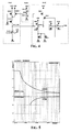
- Figure 7 and Figure 8 show simulation results of POR threshold voltage versus power up or power down time (tRAMP) with resistance values of 0.5Mohm and 1.0M ohm, respectively, in order to assess the consequent behavior of the POR threshold voltage.
- Figure 7 shows a certain lowering of the POR+ threshold voltage upon increasing the P+ resistance. Such a phenomenon can be explained by an attendant increase of the parasitic capacitance between the enlarged P+ diffusion resistor and the supply node VDD. Of course, there are parasitic capacitances of NODE_F with respect to VDD and GND.
- Figure 8 shows the POR threshold voltage behaviour in presence of a parasitic capacitance between the inverter output node NODE_F of Figure 4 and GND.
- the addition of a small junction capacitor between the output node of the input inverter of the voltage level detector of the two power on reset signal generators for compensating the parasitic capacitance of the node toward ground has been found to be effective in preventing spurious flippings of the node from a logic state to the other in case of particularly short time intervals between power off and power on phases.
- the resistive divider of the input supply voltage of the two power on reset signal generators is composed of a combination of active resistances and passive resistances of different type and selectable, for example by burning related fuses, during an EWS testing phase.
- This permits to optimize stand-by current absorption through the supply voltage dividers without compromising the dynamical response of power on reset signal generators and to select a configuration designed for a certain external power supply voltage in devices supporting two different external power supply voltages.
- FIG. 9 shows a basic functional block diagram of a semiconductor IC device with an on-chip voltage down converter (VDC) made according to this invention.
- VDC voltage down converter
- PORE_GEN is a power on reset generator of a first or primary PORE signal during external power supply voltage (VDDE) ramp up. This primary power on reset signal PORE is used for resetting not only the REF_GEN and the VDC blocks but also the secondary power on reset signal generator PORI_GEN.
- REF_GEN is a circuit that generates a stable compensated reference voltage (VREF_VDC) used by the on-chip voltage down converter VDC.
- VDC is the on-chip voltage down converter that converts the externally applied supply voltage VDDE to a stable regulated internal supply voltage (VDDI), using the reference voltage VREF_VDC for the regulation.
- PORI_GEN is the secondary power on reset signal generator that, while VDC generates the stable regulated internal supply voltage VDDI, generates the secondary power on reset signal PORI.
- This secondary power on reset signal generator is also reset by the primary PORE signal during the VDDE ramp up. In other words, the primary PORE signal cascades the secondary PORI signal during power up.
- the secondary PORI signal is the signal used for resetting and initializing core parts of the IC.
- the core parts of semiconductor device use the stable regulated internal supply voltage VDDI produced by the on-chip voltage down converter VDC and typically there is a large capacitance (Cpara) between the power supply nodes VDDI and GND.
- Figure 10 shows a circuit of PORE_GEN.
- the input and the output of PORE_GEN are the external power supply voltage VDDE and PORE, respectively.
- the circuit will contain as many POR signal generating blocks as the number of different supply voltages supported.
- one block is used for 3.0V operation, while the other is used for 1.8V operation.
- the selection of the power supply voltage may be made as shown for this embodiment by the selection fuse (Part 3), the selection being mutually exclusive by controlling VREF_POR30 or VREF_POR18.
- the compositions of the circuits are as follows.
- Partl_30 and Partl_18 are voltage dividers each composed of a PMOS active resistor and P+ diffusion and Poly resistor(s).
- VREF_POR30 is determined by dividing VDDE by the ratio between the active resistor PMOS30 and the passive resistor which is a combined Poly resistor (R30_Poly) and P+ resistor (R30_P+).
- the total passive resistance is increased to reduce stand-by current but the combination of poly resistor(s) and P+ diffusion resistor(s) in series for constituting the passive resistance portion of the input voltage divider ensures an improved POR threshold voltage dynamics and reduces the capacitance coupling of the P+ diffusion during fast power up.
- Combination of the R30_Poly and R30_P+ resistances is optimized to compromise among stand-by current, POR threshold voltage dynamics with a wide range of power up and power down times, parasitic capacitance coupling on the P+ diffusion resistor, and process spread of resistance values.
- R30_Poly must be located between the VREF_POR30 node and R30_P+ otherwise the coupling on R30_R+ will not be effectively prevented.
- C30_Poly is a parasitic capacitance between the Poly resistor and GND
- C30_P+ is a parasitic capacitance between P+ resistor and VDDE.
- C30_Poly may effectively compensate the coupling effect caused by C30_P+ during fast power up.
- PMOS30 active resistor increases the response time of VREF_POR30 when a power up with rather steep VDDE ramp occurs, so that the POR30 threshold voltage will be increased.
- VREF_POR18 is determined by dividing VDDE by the ratio between the active resistor PMOS18 and the P+ diffusion resistor (R18_P+).
- the R18_P+ value is generally moderately lower than R30_P+.
- R18_P+ resistance may be optimized to compromise between stand-by current and coupling effect.
- the active resistor PMOS 18 increases the response time during fast power up, therefore the threshold voltage POR18 will increase.
- the requirement of stand-by current in POR block is less severe because the stand-by current consumption of other blocks of Figure 9, like the VDC block is absent (the VDC in Figure 9 is normally disabled for 1.8V operation) therefore, a smaller total resistance of the input divider is tolerable.
- the use of either Part1_30 or Partl_18 depends on the requirement of stand-by current and on the parasitic capacitive coupling effect on the P+ diffusion resistor.
- Part2_30 and Part2_18 are inverter-type level detectors.
- POR30 switches to low when VREF_POR30 (VREF_POR18) reaches the logic threshold voltage of the inverter composed at one PMOS and two NMOS (PMOS0, NMOS0 and NMOS1 for 3.0V version, PMOS01, NMOS01 and NMOS11 for 1.8V version).
- NODE_F1 in Part2_1 a small capacitor on NODE_F in Part2_30 (NODE_F1 in Part2_1) for compensating the parasitic capacitance toward the ground node of the NODE_F (NODE_F1).
- This compensation capacitor Cfd or (Cfd1) may be constituted, as shown by P+ junction diode.
- NODE_F or NODE_F1
- VDDE the coupling effect on VREF_POR30 (VREF_POR18) caused by P+ diffusion resistor is effectively compensated.
- Feed back connected PMOS1, PMOS2 and NMOS2 ensure a certain hysteresis of the POR threshold value during power up and power down.
- Part3 is an optional fuse implementation of the external power supply voltage selection which selects the PMOS active resistor, R30_Poly resistor and R30_P+ resistor in Partl_30 and Part1_18, by SW30b and SW30 signals, respectively, the ability of choosing both the PMOS active resistor part and the related combination of poly and P+ passive resistors gives ample flexibility in controlling stand-by current for each selected supply voltage configuration.
- SW30b is set to “Low” and SW30 is set to “High” during power up.
- Partl_30, Part2_30 and Part3 are activated by SW30b but Partl_18 and Part2_18 remain disabled In fact, PMOS18 is off, VREF_POR18 is at GND potential through NMOS 18.
- VREF30_POR node evolves as a voltage ratio of VDDE.
- NODE_F flips and both POR30 and PORE switch to low state, driving the device into stand-by mode.
- SW30b is set to "high” and SW30 is set to "Low” during power up.
- Part1_18, Part2_18 and part3 are activated by SW30.
- Part1_30 and Part2_30 are not activated by SW30b.
- PMOS30 is off
- VREF_POR30 is set to GND through NMOS30.
- VREF18_POR node evolves as a voltage ratio of VDDE.
- NODE_F1 flips and both POR18 and PORE switch to low state, driving the device into stand-by mode.
- Figure 11 and Figure 12 shows simulation results of PORE threshold voltage versus tRAMP time.
- Figure 11 shows the result of 3.0V configuration and Figure 12 for a 1.8V configuration.
- FIG. 13 shows a simplified diagram of PORI generator.
- Input to the PORI_GEN are: VDDI and the PORE signal, and its output is PORI.
- PORI_GEN consists of three parts the details of which re as follows.
- Part1 is a voltage divider composed of a PMOS active resistor and of a P+ diffusion passive resistor.
- the P+ diffusion resistor is formed in NWELL.
- C18_P+ is a parasitic capacitance on the R18_P+ resistor
- C30_P+ is a parasitic capacitance on the R30_P+ resistor.
- the resistance value is selected by the fuse (Part3) to adapt the input divider to the selected power supply voltage ranges. For example, if the device supports the choice between 1.8V and 3.0V power supply voltages, PMOS30, R18_P+ and R30_P+ are used for 3.0V operation, PMOS18 and R18_P+ are used for 1.8V operation.
- R18_P+ is selected by an NMOS switch transistor NMOS. Circuit operation is similar to that of the primary generator PORE_GEN. The main difference is the type of passive resistor used and the resistance value. Only a P+ diffusion type resistor is used for the passive part of the voltage divider and the passive resistance is much larger than that of PORE_GEN. However, a relatively large passive P+ diffusion resistance, though significantly reducing stand-by current will exhibit an augmented capacitive coupling effect on the P+ diffusion resistor.
- the effect of a increased coupling on a larger P+ resistor is resolutively overcome by controlling the VREF_PORI input node of PORI_GEN by the primary power on reset signal PORE, through the NMOS transistor switch (NMOSP).
- Part2 is an inverter-type level detector. PORI switches to low when VREF_POR reaches the logic threshold voltage of the invert circuit, which is determined by PMOS0, NMOS0 and NMOS 1.
- a small capacitance Cfd of a P+ junction diode is connected between NODE_F and VDD to compensate for the parasitic capacitance between NODE_F and GND.
- Part3 is an optional fuse for selecting the value of total resistance of the voltage divider composed of the PMOS active resistor and the P+ passive resistor.
- FIG 14 shows the relationships among the circuit signals during operation.
- VDDI is the stable regulated supply voltage produced by the internal voltage down converter VDC
- PORE is the primary power on reset signal generated from PORE_GEN.
- VREF_PORI node after VDDE and VDDI starts rising at power up, VREF_PORI node remains in low state until the PORE signal switches to low state. When PORE switches to low, VREF_PORI node starts evolving thanks to the current flowing through the P+ resistor. When VREF_POR reaches the threshold voltage of the inverter-type level detector, NODE_F flips and the PORI switches low state, driving the device into stand-by mode.
- Figure 15 shows the relationships among signals of VDDE, VDDI, PORE and PORI. These plots are a summary of simulation results of a real sample circuit. To dotted perimeter A focus on a working condition characterized by a relatively short time interval between power down and power up or between power down and power up. It can be easily recognized that by virtue of the fact that with the novel circuit of this invention wherein the PORI generator is controlled by the primary PORE signal, PORI no longer suffers of the effects of a non-negligible time of discharge of the capacitive load represented by the parasitic capacitance. As a result, the PORI signal evolves correctly regardless of the tRAMP time of VDDE.
- the power on reset circuit of enhanced characteristics of this invention may be further provided with means for trimming the POR threshold voltage that as described above, is determined by the combination of active resistors and passive resistors in forming the voltage divider (Part1) in order to be best adapted to the actual electrical characteristics of the core parts of the IC as determined by the process spread.
- Figure 16 is another embodiment of the PORI_GEN generator characterized by including a plurality of selectable PMOS type active resistors and a plurality of selectable P+ diffusion passive resistors, all connected in series, and dedicated selection fuses FU1, FU2, FD1 and FD2, that permit, during EWS testing, to choose a certain selectable value of active resistance and a certain selectable value of passive resistance of the so configured input voltage divider of Part 1 of the circuit.
- NAND type flash devices are generally designed to ensure various values stack assembly options and in order to have sufficient flexibility of stack assembly, two of such output pins (/RB) are commonly implemented in the memory device, one of which may be used for parametric/functional test and assembly while the other one generally remains unused.
- a procedure that may be implemented before parametric and functional test of the device includes the steps of
- the fuse trimming information to get the target threshold voltage can be determined by referring to a table as the one of Figure 21. Actual values for the tested experimental device are indicated in the table of Figure 22.
Landscapes
- Engineering & Computer Science (AREA)
- Theoretical Computer Science (AREA)
- Physics & Mathematics (AREA)
- General Engineering & Computer Science (AREA)
- General Physics & Mathematics (AREA)
- Semiconductor Integrated Circuits (AREA)
- Electronic Switches (AREA)
Abstract
Description
- The present invention relates to digital integrated circuit semiconductor devices and in particular to devices including an on-chip voltage down converter for supplying core portions of the digital integrated system powerable in a low-voltage mode during certain phases of operations and precisely to an on-chip power on reset circuit.
- When an electronic system is switched on, an external power supply voltage (VDDE) is supplied to various component integrated circuit semiconductor devices and ramps up during a certain tRAMP time interval. The status of a digital semiconductor device is generally preset or initialized during power on once the supply voltage of the integrated circuits in the device has reached a correct level, in order to start operation correctly at the end of the power on phase.
- A so-called power on reset (POR) generator integrated in the device is used for initialization during power on. The generated POR signal is high until VDDE reaches a predetermined level (VPOR+) which is required for the initialization during power on, thereafter the POR signal switches to low and the semiconductor device operates in stand-by mode.
- Figure 1 shows a simplified functional block diagram of a semiconductor device, which includes an on-chip voltage down converter (VDC). A description of each block follows:
- PORE_GEN: is an "external" power on reset signal generator that generates the PORE signal during external power supply (VDDE) ramp up. The externally generated PORE signal has the function of resetting the REF_GEN and the VDC blocks.
- REF_GEN: generates a compensated stable reference voltage (VREF_VDC) that is used in an on-chip voltage down converter VDC.
- VDC: is an on-chip voltage down converter that converts VDDE to a stable regulated internal voltage supply (VDDI) using VREF_VDC for regulating it.
- PORI_GEN: is an "internal" power on reset generator that generates the internal signal PORI when a stable regulated internal voltage supply VDDI is produced by the VDC block. The PORI signal is used for resetting and initializing core parts of the IC.
- The core parts of the semiconductor device use the stable regulated internal supply voltage VDDI produced by the on-chip VDC and typically there is a large capacitance between VDDI and GND.
- Figure 2 shows a simplified PORE dynamics when VDDE is powered up and powered down with ramping time tRAMP.
- During VDDE ramp up, POR follows VDDE, (POR is in 'High' state until VDDE reaches predetermined level (VPOR_TH+: POR threshold voltage during power up); POR 'High' keeps the device in reset condition. During VDDE ramp down, POR switches to 'High' state when VDDE is lower than VPOR_TH-(POR threshold voltage during power down). The difference between VPOR_TH+ and VPOR_TH- ensures a hysteresis for filtering out the noise in the power supply voltage during the power up period.
- Figure 3 shows a simplified PORI dynamics when VDDE is ramping up and down with tRAMP time, and VDDI is being generated by VDC converting the external supplying voltage VDDE. Due to this conversion, the VDC response time induces a time lag between VDDE and VDDI during power up and down. During power down of VDDE and VDDI there is an additional time lag due to the capacitive load (Cpara) between the VDDI made that needs time to be discharged and GND. It may be observed that the relationship between PORI and VDDI is almost the same as that of PORE and VDDE.
- Figure 4 shows a basic circuit diagram used for both the first or primary power on reset circuit PORE_GEN and for the second or secondary power on reset circuit PORI_GEN.
- The two circuits are identical and function with VDD equal to the external VDDE and VDDI respectively.
- The circuit consists of three parts and the details of each part are explained as follows.
- Part1 is a non linear voltage divider composed of a PMOS active resistor and P+ diffusion passive resistor. The PMOS active resistor enhances the response time when power up ramping time is fast, while the P+ passive resistor formed on a NWELL guarantees a stable resistance value with respect to process spread and prevents possible ground bouncing during internal operation. On the other hand, an active P+ diffusion resistor introduces a parasitic capacitance between the P+ diffusion and VDD.
- Part2 is an inverter-type level detector. The POR signal switches to low when VREF_POR reaches the logic threshold of the inverter made of PMOS0, NMOS0 and NMOS1. Feed back network connected to PMOS1, PMOS2 and NMOS2 provide for a certain hysteresis of POR threshold voltage during power up and power down.
- Part3 is an optional fuse for selecting a PMOS active resistor value in the Part1 current implemented to provide a choice between different external power supply voltage ratings of the device, such as for either a 1.8V or a 3.0V supply voltage.
- For example, considering the PORE_GEN, when VDD starts rising, the VREF_POR voltage evolves as a voltage ratio of the input supply voltage VDDE. When VREF_POR reaches the threshold voltage of the level detector, the NODE_F flips and the PORE signal switches to low state, driving the device to stand-by mode.
- During stand-by mode, there is a static DC current flowing in the POR circuit according to the equation I= VREF_POR/ (Resistance of P+ diffusion resistor).
- Figure 5 shows the simulation results for different tRAMP with VDD=3.0V and resistance of P+ 0.25 Mohm.
- With a relatively short tRMAP (fast power up // power down), the POR signal is generated at higher (/lower) voltage than VPOR+min (/VPOR-max) because the parasitic capacitance on VREF_POR increases its precharge (/discharge) time through the PMOS (/P+) resistor. With relatively long tRAMP (slow power up// power down), the POR signal is generated in almost coincidence with the VPOR+min (/VPOR-max).
- The drawbacks of known POR circuits as the one described above may be summarized as follows.
- Firstly, the known circuits are unable to work reliably when the time interval between power down and power up becomes very short.
- Figure 6 shows the relationships among signals; VDDE, VDDI, PORE and PORI. When the time interval between power down and power up is short (re: dotted circle A), VDDI can't follow up VDDE because VDDI needs time to discharge the capacitive load (Cpara of Figure 1), therefore the PORI does not operate correctly as it becomes unable to detect a VDDE glitch.
- Secondly, the known circuits have an unwanted coupling effect caused by parasitic capacitance when P+ resistance value is increased for reducing stand-by current absorption.
- Figure 7 and Figure 8 show simulation results of POR threshold voltage versus power up or power down time (tRAMP) with resistance values of 0.5Mohm and 1.0M ohm, respectively, in order to assess the consequent behavior of the POR threshold voltage. Figure 7 shows a certain lowering of the POR+ threshold voltage upon increasing the P+ resistance. Such a phenomenon can be explained by an attendant increase of the parasitic capacitance between the enlarged P+ diffusion resistor and the supply node VDD. Of course, there are parasitic capacitances of NODE_F with respect to VDD and GND.
- Figure 8 shows the POR threshold voltage behaviour in presence of a parasitic capacitance between the inverter output node NODE_F of Figure 4 and GND.
- On another account, minimizing static DC current absorption during stand-by mode in a POR circuit by increasing the passive resistance portion of the input supply voltage divider is a generally attendant requisite of digital devices.
- The applicants have tried several approaches to reduce the stand-by current, however, as resumed herein below, these attempts were unsuccessful because of accompanying drawbacks:
- a) replacing the P+ resistor with an N+ resistor and increasing the resistance. With this approach, a very good POR threshold dynamics is achieved during power up, but unsatisfactory during power down because the N+ resistor is formed on a P-substrate biased to GND, therefore there is a large parasitic capacitance between N+ resistor and GND.
- b) replacing the P+ resistor with a poly resistor and increasing the resistance. With this approach, the POR threshold dynamics is very good during power up, but again quite unsatisfactory during power down due to the large parasitic capacitance between the poly resistor and GND. Moreover, the resistance of the poly resistor is subject to large process variations, which results in large spread of VPOR+.
- c) use of a large P+ resistor and addition of a compensating capacitor between VREF_POR and GND. With this approach the POR threshold dynamics is very good during power up, but unsatisfactory during power down due to the time of discharge to GND through the P+ resistor.
- In their search for a solution to these baffling shortcomings of known power on reset circuits, the applicant have found an outstandingly effective solution that is based on the intuition of making the primary power on rest signal generated during external power supply voltage ramp up not only reset the reference voltage generator and the voltage down converter but also the secondary power on reset signal generator, practically cascading the later from the primary power on reset signal.
- Moreover, according to a preferred embodiment of the circuits of this invention, the addition of a small junction capacitor between the output node of the input inverter of the voltage level detector of the two power on reset signal generators for compensating the parasitic capacitance of the node toward ground, has been found to be effective in preventing spurious flippings of the node from a logic state to the other in case of particularly short time intervals between power off and power on phases.
- Preferably, the resistive divider of the input supply voltage of the two power on reset signal generators is composed of a combination of active resistances and passive resistances of different type and selectable, for example by burning related fuses, during an EWS testing phase. This permits to optimize stand-by current absorption through the supply voltage dividers without compromising the dynamical response of power on reset signal generators and to select a configuration designed for a certain external power supply voltage in devices supporting two different external power supply voltages. The invention is defined in the dependent claims.
-
- Figure 1 shows a simplified functional block diagram of a semiconductor device, which includes an on-chip voltage down converter (VDC).
- Figure 2 shows a simplified PORE dynamics when VDDE is powered up and powered down with ramping time tRAMP.
- Figure 3 shows a simplified PORI dynamics when VDDE is ramping up and down with tRAMP time, and VDDI is being generated by an on-chip down converter of the external supply voltage VDDE.
- Figure 4 shows a basic circuit diagram commonly used for both the first or primary power on reset circuit PORE_GEN and for the second or secondary power on reset circuit PORI_GEN.
- Figure 5 shows the simulation results for different tRAMP with a power supply voltage of 3.0V and a P+ diffusion passive resistance of 0.25Mohm.
- Figure 6 shows dynamic relationships among signals; VDDE, VDDI, PORE and PORI.
- Figures 7 and 8 show simulation results of POR threshold voltage versus power up or power down time (tRAMP) with input divider resistance values of 0.5Mohm and 1.0M ohm, respectively.
- Figure 9 is a basic block diagram of a semiconductor IC device with an on-chip voltage down converter made according to this invention.
- Figure 10 shows an embodiment of a two selectable module PORE_GEN circuit of the block diagram of Figure 9.
- Figure 11 and Figure 12 shows simulation results of PORE threshold voltage versus tRAMP time.
- Figure 13 shows an embodiment of the PORI_GEN circuit of the block diagram of Figure 9.
- Figure 14 shows dynamic relationships among signals in the circuit of Figure 13.
- Figure 15 shows the relationships among signals of VDDE, VDDI, PORE and PORI for the circuit of this invention.
- Figure 16 is an alternative and preferred embodiment of the PORI_GEN generator circuit.
- Figures 17-22 relate to a power on reset circuit trimming procedure implementable before parametric and functional test of a NAND flash memory device provided with the power on reset circuit according to the embodiment of Figure 16.
- Figure 9 shows a basic functional block diagram of a semiconductor IC device with an on-chip voltage down converter (VDC) made according to this invention.
- PORE_GEN is a power on reset generator of a first or primary PORE signal during external power supply voltage (VDDE) ramp up. This primary power on reset signal PORE is used for resetting not only the REF_GEN and the VDC blocks but also the secondary power on reset signal generator PORI_GEN.
- REF_GEN is a circuit that generates a stable compensated reference voltage (VREF_VDC) used by the on-chip voltage down converter VDC.
- VDC is the on-chip voltage down converter that converts the externally applied supply voltage VDDE to a stable regulated internal supply voltage (VDDI), using the reference voltage VREF_VDC for the regulation.
- PORI_GEN is the secondary power on reset signal generator that, while VDC generates the stable regulated internal supply voltage VDDI, generates the secondary power on reset signal PORI. This secondary power on reset signal generator is also reset by the primary PORE signal during the VDDE ramp up. In other words, the primary PORE signal cascades the secondary PORI signal during power up. The secondary PORI signal is the signal used for resetting and initializing core parts of the IC.
- The core parts of semiconductor device use the stable regulated internal supply voltage VDDI produced by the on-chip voltage down converter VDC and typically there is a large capacitance (Cpara) between the power supply nodes VDDI and GND.
- Figure 10 shows a circuit of PORE_GEN. The input and the output of PORE_GEN are the external power supply voltage VDDE and PORE, respectively. In practice, the circuit will contain as many POR signal generating blocks as the number of different supply voltages supported.
- For example, if device supports 3.0V and 1.8V operation, one block is used for 3.0V operation, while the other is used for 1.8V operation.
- The selection of the power supply voltage may be made as shown for this embodiment by the selection fuse (Part 3), the selection being mutually exclusive by controlling VREF_POR30 or VREF_POR18. The compositions of the circuits are as follows.
- Partl_30 and Partl_18 are voltage dividers each composed of a PMOS active resistor and P+ diffusion and Poly resistor(s).
- Part1_30 is used for 3.0V operation VREF_POR30 is determined by dividing VDDE by the ratio between the active resistor PMOS30 and the passive resistor which is a combined Poly resistor (R30_Poly) and P+ resistor (R30_P+).
- The total passive resistance is increased to reduce stand-by current but the combination of poly resistor(s) and P+ diffusion resistor(s) in series for constituting the passive resistance portion of the input voltage divider ensures an improved POR threshold voltage dynamics and reduces the capacitance coupling of the P+ diffusion during fast power up. Combination of the R30_Poly and R30_P+ resistances is optimized to compromise among stand-by current, POR threshold voltage dynamics with a wide range of power up and power down times, parasitic capacitance coupling on the P+ diffusion resistor, and process spread of resistance values.
- R30_Poly must be located between the VREF_POR30 node and R30_P+ otherwise the coupling on R30_R+ will not be effectively prevented. C30_Poly is a parasitic capacitance between the Poly resistor and GND, C30_P+ is a parasitic capacitance between P+ resistor and VDDE. C30_Poly may effectively compensate the coupling effect caused by C30_P+ during fast power up.
- PMOS30 active resistor increases the response time of VREF_POR30 when a power up with rather steep VDDE ramp occurs, so that the POR30 threshold voltage will be increased.
- Part1_18 is used for 1.8V operation VREF_POR18 is determined by dividing VDDE by the ratio between the active resistor PMOS18 and the P+ diffusion resistor (R18_P+). The R18_P+ value is generally moderately lower than R30_P+.
- A parasitic capacitance exists between C18_P+ and VDDE. R18_P+ resistance may be optimized to compromise between stand-by current and coupling effect. The active resistor PMOS 18 increases the response time during fast power up, therefore the threshold voltage POR18 will increase. In case of 1.8V operation, the requirement of stand-by current in POR block is less severe because the stand-by current consumption of other blocks of Figure 9, like the VDC block is absent (the VDC in Figure 9 is normally disabled for 1.8V operation) therefore, a smaller total resistance of the input divider is tolerable. The use of either Part1_30 or Partl_18 depends on the requirement of stand-by current and on the parasitic capacitive coupling effect on the P+ diffusion resistor.
- Part2_30 and Part2_18 are inverter-type level detectors. POR30 (POR18) switches to low when VREF_POR30 (VREF_POR18) reaches the logic threshold voltage of the inverter composed at one PMOS and two NMOS (PMOS0, NMOS0 and NMOS1 for 3.0V version, PMOS01, NMOS01 and NMOS11 for 1.8V version).
- In addition, according to an important feature of the circuit there is a small capacitor on NODE_F in Part2_30 (NODE_F1 in Part2_1) for compensating the parasitic capacitance toward the ground node of the NODE_F (NODE_F1).
- This compensation capacitor Cfd or (Cfd1) may be constituted, as shown by P+ junction diode. By adding this small capacitance between NODE_F (or NODE_F1) to VDDE the coupling effect on VREF_POR30 (VREF_POR18) caused by P+ diffusion resistor is effectively compensated. Feed back connected PMOS1, PMOS2 and NMOS2 (PMOS11, PMOS21 and NMOS21) ensure a certain hysteresis of the POR threshold value during power up and power down.
- As already said, Part3 is an optional fuse implementation of the external power supply voltage selection which selects the PMOS active resistor, R30_Poly resistor and R30_P+ resistor in Partl_30 and Part1_18, by SW30b and SW30 signals, respectively, the ability of choosing both the PMOS active resistor part and the related combination of poly and P+ passive resistors gives ample flexibility in controlling stand-by current for each selected supply voltage configuration.
- SW30b is set to "Low" and SW30 is set to "High" during power up.
- Partl_30, Part2_30 and Part3 are activated by SW30b but Partl_18 and Part2_18 remain disabled In fact, PMOS18 is off, VREF_POR18 is at GND potential through NMOS 18.
- After VDDE starts rising at power up, VREF30_POR node evolves as a voltage ratio of VDDE. When VREF30_POR reaches the threshold voltage of the inverter-type level detector, NODE_F flips and both POR30 and PORE switch to low state, driving the device into stand-by mode.
- During stand-by mode, a static DC current flow in the PORE_GEN circuit flows but it is relatively small due to the fact that total flow path resistance is large.
- SW30b is set to "high" and SW30 is set to "Low" during power up. Part1_18, Part2_18 and part3 are activated by SW30. Contrarily, Part1_30 and Part2_30 are not activated by SW30b. In fact, PMOS30 is off, VREF_POR30 is set to GND through NMOS30.
- After VDDE starts rising at power up, VREF18_POR node evolves as a voltage ratio of VDDE. When VREF18_POR reaches the threshold voltage of the inverter-type level detector, NODE_F1 flips and both POR18 and PORE switch to low state, driving the device into stand-by mode.
- During stand-by mode, there is a static DC current flowing in PORE_GEN circuit, but it is relatively small.
- Figure 11 and Figure 12 shows simulation results of PORE threshold voltage versus tRAMP time. Figure 11 shows the result of 3.0V configuration and Figure 12 for a 1.8V configuration.
- The results show that the POR threshold dynamics retains excellent characteristics notwithstanding the use of a relatively large resistance on VREF_POR30 (VREF_POR18), thus keeping the stand-by current low.
- Figure 13 shows a simplified diagram of PORI generator. Input to the PORI_GEN are: VDDI and the PORE signal, and its output is PORI. According to a preferred embodiment, PORI_GEN consists of three parts the details of which re as follows.
- Part1 is a voltage divider composed of a PMOS active resistor and of a P+ diffusion passive resistor.
- The P+ diffusion resistor is formed in NWELL. C18_P+ is a parasitic capacitance on the R18_P+ resistor, C30_P+ is a parasitic capacitance on the R30_P+ resistor. The resistance value is selected by the fuse (Part3) to adapt the input divider to the selected power supply voltage ranges. For example, if the device supports the choice between 1.8V and 3.0V power supply voltages, PMOS30, R18_P+ and R30_P+ are used for 3.0V operation, PMOS18 and R18_P+ are used for 1.8V operation.
- R18_P+ is selected by an NMOS switch transistor NMOS. Circuit operation is similar to that of the primary generator PORE_GEN. The main difference is the type of passive resistor used and the resistance value. Only a P+ diffusion type resistor is used for the passive part of the voltage divider and the passive resistance is much larger than that of PORE_GEN. However, a relatively large passive P+ diffusion resistance, though significantly reducing stand-by current will exhibit an augmented capacitive coupling effect on the P+ diffusion resistor.
- According to the essential aspect of this invention, the effect of a increased coupling on a larger P+ resistor is resolutively overcome by controlling the VREF_PORI input node of PORI_GEN by the primary power on reset signal PORE, through the NMOS transistor switch (NMOSP).
- Part2 is an inverter-type level detector. PORI switches to low when VREF_POR reaches the logic threshold voltage of the invert circuit, which is determined by PMOS0, NMOS0 and
NMOS 1. - Also in the PORI_GEN circuit, a small capacitance Cfd of a P+ junction diode is connected between NODE_F and VDD to compensate for the parasitic capacitance between NODE_F and GND.
- Part3 is an optional fuse for selecting the value of total resistance of the voltage divider composed of the PMOS active resistor and the P+ passive resistor.
- Figure 14 shows the relationships among the circuit signals during operation. As we explained in relation to the basic diagram of Figure 9, VDDI is the stable regulated supply voltage produced by the internal voltage down converter VDC and PORE is the primary power on reset signal generated from PORE_GEN.
- According to this invention, after VDDE and VDDI starts rising at power up, VREF_PORI node remains in low state until the PORE signal switches to low state. When PORE switches to low, VREF_PORI node starts evolving thanks to the current flowing through the P+ resistor. When VREF_POR reaches the threshold voltage of the inverter-type level detector, NODE_F flips and the PORI switches low state, driving the device into stand-by mode.
- The waveforms demonstrate that there is not any observable effect of the capacitive coupling on P+ diffusion resistor notwithstanding the use of a much larger resistance on VREF_PORI compared to the maximum resistance that was tolerable to integrate in the known circuits.
- Figure 15 shows the relationships among signals of VDDE, VDDI, PORE and PORI. These plots are a summary of simulation results of a real sample circuit. To dotted perimeter A focus on a working condition characterized by a relatively short time interval between power down and power up or between power down and power up. It can be easily recognized that by virtue of the fact that with the novel circuit of this invention wherein the PORI generator is controlled by the primary PORE signal, PORI no longer suffers of the effects of a non-negligible time of discharge of the capacitive load represented by the parasitic capacitance. As a result, the PORI signal evolves correctly regardless of the tRAMP time of VDDE.
- The above described novel power on reset circuit of greatly enhanced performance both in terms of reliability of operations even with reduced time intervals between on and off switchings of the device, is useful in a variety of digital ICs, including devices such as for example NAND type flash memories that are particularly sensitive to internal signal instabilities at power on.
- Moreover, the electrical properties of certain digital devices as flash memories and even more so multilevel flash memories are subject to process spread of significant magnitude.
- For critical applications as those mentioned above, the power on reset circuit of enhanced characteristics of this invention may be further provided with means for trimming the POR threshold voltage that as described above, is determined by the combination of active resistors and passive resistors in forming the voltage divider (Part1) in order to be best adapted to the actual electrical characteristics of the core parts of the IC as determined by the process spread.
- Figure 16 is another embodiment of the PORI_GEN generator characterized by including a plurality of selectable PMOS type active resistors and a plurality of selectable P+ diffusion passive resistors, all connected in series, and dedicated selection fuses FU1, FU2, FD1 and FD2, that permit, during EWS testing, to choose a certain selectable value of active resistance and a certain selectable value of passive resistance of the so configured input voltage divider of
Part 1 of the circuit. - Increasing the value of the PMOS active resistance lowers the level of the Vref_pore that increases the pore threshold voltage.
- Conversely, by decreasing the value of the P+ passive resistance the level of the Vref_pore rises, which in turn decreases the secondary PORI_GEN threshold voltage.
- In case of a NAND flash memory, as it is well known to a skilled technician, at least a ready/busy (/RB) output pin in the form of an open drain output is often employed for indicating the status of the device. On the other hand, NAND type flash devices are generally designed to ensure various values stack assembly options and in order to have sufficient flexibility of stack assembly, two of such output pins (/RB) are commonly implemented in the memory device, one of which may be used for parametric/functional test and assembly while the other one generally remains unused.
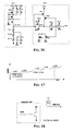
- As depicted in Figure 18, such an unused /RB pad may be exploited for permitting monitoring the internally generated PORI signal during a power on reset threshold voltage trimming procedure, as allowed by the embodiment of the PORI_GEN circuit of Figure 16, described above.
- A procedure that may be implemented before parametric and functional test of the device, includes the steps of
- step 1) applying to the device an external supply voltage (VDDE) through a staircase ramp up, as graphically depicted in Figure 17;
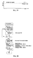
- step 2) monitoring through the available spare RB pad of the device or through a dedicated pad, the evolution of the power on reset signal, a result of which is depicted in Figure 19;
- step 3) if the POR threshold level is high go back to the first step and if pore threshold level is low continue with the next step;
- step 4) reading the VDDE voltage while POR level is low such that the read voltage gives a measured POR threshold voltage (VTH meas.).;
- step 5) extracting POR threshold trimming information based on the measured POR threshold voltage (VTH meas.);
- step 6) trimming down or up, depending on the difference between the measured POR threshold voltage (VTH meas.) and the target POR threshold voltage Vpore_TH+(VTH0), according to the minimum trimming voltage difference implementable in the trimmable input voltage divider of the PORI_GEN circuit of Figure 16;
- step 7) burning the selected fuses.
- The above described procedure is graphically illustrated in the form of a flow chart in Figure 20.
- After having read the measured POR threshold voltage, the fuse trimming information to get the target threshold voltage (VTH0) can be determined by referring to a table as the one of Figure 21. Actual values for the tested experimental device are indicated in the table of Figure 22.
Claims (5)
- A power on reset circuit for initializing a digital integrated circuit at power on, comprising
a first power on reset signal generator (PORE_GEN) supplied by an externally applied power supply voltage (VDDE), generating a first or external power on reset signal (PORE) during external power supply voltage (VDDE) ramp up, a reference voltage generator (REF_GEN) powered by said externally applied power supply voltage (VDDE) when enabled by said first power on reset signal (PORE) for generating a stable compensating reference voltage (VREF_VDC),
a voltage down converter circuit (VDC) converting the externally applied power supply voltage (VDDE) to a stable regulated internal supply voltage (VDDI) employing said reference voltage (VREF_VDC) generated by the reference voltage generator,
and a second or internal power on reset signal generator circuit (PORI_GEN) supplied at said stable regulated internal supply voltage (VDDI) and generating a second power on reset signal (PORI) conveyed to core parts of the integrated circuit for initializing them at power on, characterized in that also the second internal power on reset signal generator circuit has enablement means for enabling the generator circuit with said first power on reset signal (PORE) together with said voltage down converter circuit (VDC). - The power on reset circuit of claim 1, characterized in that said first power on reset generator (PORE_GEN) and said second power on reset signal generator (PORI_GEN) comprise a first part (Part1) constituted by a non linear voltage divider of the input power supply voltage, composed of an active resistance portion and a passive resistance portion, and by a second part (Part2) consisting in an inverter-type level detector circuit, characterized in that the output node of an input inverter, the input node which is connected to an intermediate node of said voltage divider, is capacitively coupled to the power supply node by a capacitor (Cfd) for compensating the parasitic capacitance toward ground of said output node.
- The power on reset circuit of claim 1, wherein said first power on reset signal generator (PORE_GEN) is duplicated in two mutually exclusive selectable modules for two external power supply voltage ratings, respectively, of the device, both modules have said active resistance portion of the input supply voltage divider (Part1) comprising a PMOS transistor, the module selected for low supply voltage mode of the externally powered device has said passive portion of the input voltage divider (Part1) including an additional polysilicon resistor in series to a P+ diffusion resistor, fuse means (Part3) for coupling to ground (GDN) a control gate of said PMOS transistor, for selecting the high supply voltage mode, or for coupling to the input supply voltage node, for selecting the low supply voltage mode.
- The power on reset circuit for a device according to claim 2, wherein said second power on reset signal generator (PORI_GEN) has both said active resistance portion and said passive resistance portion of said input voltage divider comprising a plurality of series connected components individually disableable by associated by-pass fuse means for trimming dynamic response and current absorption characteristics during a EWS testing phase of the fabrication process of the device.
- A NAND type flash memory device including a power on reset circuit according to claim 4.
Priority Applications (4)
| Application Number | Priority Date | Filing Date | Title |
|---|---|---|---|
| EP06425538A EP1883160B1 (en) | 2006-07-28 | 2006-07-28 | Power on reset circuit for a digital device including an on-chip voltage down converter |
| DE602006002886T DE602006002886D1 (en) | 2006-07-28 | 2006-07-28 | Operational reset circuit for a digital device with on-chip voltage-down converter |
| US11/829,413 US7602225B2 (en) | 2006-07-28 | 2007-07-27 | Power on reset circuit for a digital device including an on-chip voltage down converter |
| CN2007101371206A CN101114827B (en) | 2006-07-28 | 2007-07-30 | Power on reset circuit for a digital device including an on-chip voltage down converter |
Applications Claiming Priority (1)
| Application Number | Priority Date | Filing Date | Title |
|---|---|---|---|
| EP06425538A EP1883160B1 (en) | 2006-07-28 | 2006-07-28 | Power on reset circuit for a digital device including an on-chip voltage down converter |
Publications (2)
| Publication Number | Publication Date |
|---|---|
| EP1883160A1 true EP1883160A1 (en) | 2008-01-30 |
| EP1883160B1 EP1883160B1 (en) | 2008-09-24 |
Family
ID=37551903
Family Applications (1)
| Application Number | Title | Priority Date | Filing Date |
|---|---|---|---|
| EP06425538A Not-in-force EP1883160B1 (en) | 2006-07-28 | 2006-07-28 | Power on reset circuit for a digital device including an on-chip voltage down converter |
Country Status (4)
| Country | Link |
|---|---|
| US (1) | US7602225B2 (en) |
| EP (1) | EP1883160B1 (en) |
| CN (1) | CN101114827B (en) |
| DE (1) | DE602006002886D1 (en) |
Families Citing this family (21)
| Publication number | Priority date | Publication date | Assignee | Title |
|---|---|---|---|---|
| JP5251499B2 (en) * | 2008-12-26 | 2013-07-31 | 富士通セミコンダクター株式会社 | Semiconductor device, startup control method and system for semiconductor device |
| US7952402B2 (en) * | 2009-02-06 | 2011-05-31 | Standard Microsystems Corporation | Power-up control for very low-power systems |
| CN101697171B (en) * | 2009-09-15 | 2012-06-13 | 苏州超锐微电子有限公司 | Method for simulating power-on reset on special integrated circuit on FPGA (field programmable gate array) |
| JP5607963B2 (en) * | 2010-03-19 | 2014-10-15 | スパンション エルエルシー | Reference voltage circuit and semiconductor integrated circuit |
| TWI505075B (en) * | 2012-01-10 | 2015-10-21 | Green Solution Tech Co Ltd | Power-good signal generator and controller with power sequencingfree |
| CN102710241B (en) * | 2012-05-08 | 2015-06-03 | 卓捷创芯科技(深圳)有限公司 | Passive radio-frequency recognition power-on-reset circuit and passive radio-frequency recognition tag |
| JP5852537B2 (en) * | 2012-09-25 | 2016-02-03 | ルネサスエレクトロニクス株式会社 | Semiconductor device |
| CN103873036B (en) * | 2012-12-14 | 2017-02-22 | 普诚科技股份有限公司 | Power-on reset circuit |
| CN104007800B (en) * | 2013-02-27 | 2018-02-27 | 联想(北京)有限公司 | A kind of reset circuit, electronic equipment and repositioning method |
| JP6088306B2 (en) * | 2013-03-18 | 2017-03-01 | エスアイアイ・セミコンダクタ株式会社 | Light receiving circuit |
| CN103346779B (en) * | 2013-06-26 | 2016-01-06 | 成都鸿芯纪元科技有限公司 | A kind of FPGA on-chip low power consumption |
| CN104635822B (en) * | 2013-11-12 | 2016-07-27 | 奇景光电股份有限公司 | Power On Reset Circuit |
| CN103746681B (en) * | 2013-12-24 | 2017-06-30 | 北京时代民芯科技有限公司 | A kind of upper and lower electricity output tri-state control circuit of cmos device power supply |
| KR20170006980A (en) * | 2015-07-10 | 2017-01-18 | 에스케이하이닉스 주식회사 | Power on reset circuit and semiconductor memory device having the same |
| KR20170034524A (en) | 2015-09-21 | 2017-03-29 | 에스케이하이닉스 주식회사 | Initial signal generating device and non-volatile memory apparatus using the same |
| DE102016102696A1 (en) * | 2016-02-16 | 2017-08-17 | Infineon Technologies Ag | Apparatus and method for internal reset signal generation |
| CN105811941B (en) * | 2016-04-08 | 2017-05-17 | 厦门新页微电子技术有限公司 | Power-on reset circuit |
| KR20180111157A (en) * | 2017-03-31 | 2018-10-11 | 에스케이하이닉스 주식회사 | Controller and operating method of controller |
| CN110875733A (en) * | 2018-09-03 | 2020-03-10 | 雅特力科技(重庆)有限公司 | Power-on reset signal generator and related electronic device |
| KR102761445B1 (en) * | 2020-07-21 | 2025-02-03 | 에스케이하이닉스 주식회사 | Semiconductor apparatus and semiconductor memory apparatus |
| US11502679B2 (en) * | 2020-08-13 | 2022-11-15 | Macronix International Co., Ltd. | Robust power-on-reset circuit with body effect technique |
Citations (4)
| Publication number | Priority date | Publication date | Assignee | Title |
|---|---|---|---|---|
| US4812679A (en) * | 1987-11-09 | 1989-03-14 | Motorola, Inc. | Power-on reset circuit |
| US5519347A (en) * | 1993-11-08 | 1996-05-21 | Samsung Electronics Co., Ltd. | Start-up circuit for stable power-on of semiconductor memory device |
| US20020031032A1 (en) * | 1994-08-04 | 2002-03-14 | Tsukasa Ooishi | Semiconductor memory device with a voltage down converter stably generating an internal down-converted voltage |
| WO2004057449A2 (en) * | 2002-12-20 | 2004-07-08 | Koninklijke Philips Electronics N.V. | Power supply level monitoring and reset generation |
Family Cites Families (3)
| Publication number | Priority date | Publication date | Assignee | Title |
|---|---|---|---|---|
| JP3650186B2 (en) * | 1995-11-28 | 2005-05-18 | 株式会社ルネサステクノロジ | Semiconductor device and comparison circuit |
| DE19743347C2 (en) * | 1997-09-30 | 1999-08-12 | Siemens Ag | RS flip-flop with enable inputs |
| US6480967B1 (en) * | 1999-05-21 | 2002-11-12 | Koninklijke Philips Electronics N.V. | Multiple module processing system with reset system independent of reset characteristics of the modules |
-
2006
- 2006-07-28 DE DE602006002886T patent/DE602006002886D1/en active Active
- 2006-07-28 EP EP06425538A patent/EP1883160B1/en not_active Not-in-force
-
2007
- 2007-07-27 US US11/829,413 patent/US7602225B2/en active Active
- 2007-07-30 CN CN2007101371206A patent/CN101114827B/en active Active
Patent Citations (4)
| Publication number | Priority date | Publication date | Assignee | Title |
|---|---|---|---|---|
| US4812679A (en) * | 1987-11-09 | 1989-03-14 | Motorola, Inc. | Power-on reset circuit |
| US5519347A (en) * | 1993-11-08 | 1996-05-21 | Samsung Electronics Co., Ltd. | Start-up circuit for stable power-on of semiconductor memory device |
| US20020031032A1 (en) * | 1994-08-04 | 2002-03-14 | Tsukasa Ooishi | Semiconductor memory device with a voltage down converter stably generating an internal down-converted voltage |
| WO2004057449A2 (en) * | 2002-12-20 | 2004-07-08 | Koninklijke Philips Electronics N.V. | Power supply level monitoring and reset generation |
Non-Patent Citations (1)
| Title |
|---|
| BENZER R: "WHAT TO DO WHEN THE POWER GOES OUT", MACHINE DESIGN, PENTON MEDIA, CLEVELAND, OH, US, vol. 63, no. 7, 11 April 1991 (1991-04-11), pages 62 - 63, XP000212738, ISSN: 0024-9114 * |
Also Published As
| Publication number | Publication date |
|---|---|
| CN101114827A (en) | 2008-01-30 |
| DE602006002886D1 (en) | 2008-11-06 |
| EP1883160B1 (en) | 2008-09-24 |
| CN101114827B (en) | 2012-11-14 |
| US20080048743A1 (en) | 2008-02-28 |
| US7602225B2 (en) | 2009-10-13 |
Similar Documents
| Publication | Publication Date | Title |
|---|---|---|
| US7602225B2 (en) | Power on reset circuit for a digital device including an on-chip voltage down converter | |
| KR100285184B1 (en) | Step-up Circuits and Semiconductor Memory Devices | |
| KR100427204B1 (en) | Semiconductor device | |
| US5894423A (en) | Data processing system having an auto-ranging low voltage detection circuit | |
| US20050180076A1 (en) | Electrostatic discharge protection circuit | |
| US20140021985A1 (en) | Semiconductor device including power-on reset circuit | |
| US20090154035A1 (en) | ESD Protection Circuit | |
| JPH0214814B2 (en) | ||
| US20110156802A1 (en) | Charge pump with low power, high voltage protection circuitry | |
| US7126872B2 (en) | Semiconductor integrated circuit | |
| US10839921B2 (en) | Circuits for bleeding supply voltage from a device in a power down state | |
| US6778000B2 (en) | Integrated circuit devices that provide constant time delays irrespective of temperature variation | |
| EP0473193A2 (en) | Semiconductor device having a temperature detection circuit | |
| US20150061631A1 (en) | Semiconductor device and current amount control method | |
| US6614674B2 (en) | Regulator circuit for independent adjustment of pumps in multiple modes of operation | |
| KR102936060B1 (en) | Measure the voltage level of the voltage node using a measurement integrated circuit. | |
| EP3451338B1 (en) | Power supply ready indicator circuit | |
| JP2022044133A (en) | Semiconductor integrated circuit for power supply | |
| CN101714866A (en) | Semiconductor device and method of supplying internal power to semiconductor device | |
| CN118353235A (en) | Power application circuit | |
| US9871509B2 (en) | Power-on reset circuit | |
| JP2006511161A (en) | Power supply level monitoring and reset generation | |
| JPH03283562A (en) | Semiconductor ic device | |
| US20070030046A1 (en) | Delay cell using a capacitor displacement current | |
| KR20000015676A (en) | Power on reset circuit of semiconductor memory device |
Legal Events
| Date | Code | Title | Description |
|---|---|---|---|
| PUAI | Public reference made under article 153(3) epc to a published international application that has entered the european phase |
Free format text: ORIGINAL CODE: 0009012 |
|
| 17P | Request for examination filed |
Effective date: 20070713 |
|
| AK | Designated contracting states |
Kind code of ref document: A1 Designated state(s): AT BE BG CH CY CZ DE DK EE ES FI FR GB GR HU IE IS IT LI LT LU LV MC NL PL PT RO SE SI SK TR |
|
| AX | Request for extension of the european patent |
Extension state: AL BA HR MK YU |
|
| GRAP | Despatch of communication of intention to grant a patent |
Free format text: ORIGINAL CODE: EPIDOSNIGR1 |
|
| GRAS | Grant fee paid |
Free format text: ORIGINAL CODE: EPIDOSNIGR3 |
|
| GRAA | (expected) grant |
Free format text: ORIGINAL CODE: 0009210 |
|
| AK | Designated contracting states |
Kind code of ref document: B1 Designated state(s): DE FR GB IT |
|
| REG | Reference to a national code |
Ref country code: GB Ref legal event code: FG4D |
|
| AKX | Designation fees paid |
Designated state(s): DE FR GB IT |
|
| REF | Corresponds to: |
Ref document number: 602006002886 Country of ref document: DE Date of ref document: 20081106 Kind code of ref document: P |
|
| PLBE | No opposition filed within time limit |
Free format text: ORIGINAL CODE: 0009261 |
|
| STAA | Information on the status of an ep patent application or granted ep patent |
Free format text: STATUS: NO OPPOSITION FILED WITHIN TIME LIMIT |
|
| PG25 | Lapsed in a contracting state [announced via postgrant information from national office to epo] |
Ref country code: IT Free format text: LAPSE BECAUSE OF FAILURE TO SUBMIT A TRANSLATION OF THE DESCRIPTION OR TO PAY THE FEE WITHIN THE PRESCRIBED TIME-LIMIT Effective date: 20080924 |
|
| 26N | No opposition filed |
Effective date: 20090625 |
|
| REG | Reference to a national code |
Ref country code: FR Ref legal event code: ST Effective date: 20100331 |
|
| PG25 | Lapsed in a contracting state [announced via postgrant information from national office to epo] |
Ref country code: FR Free format text: LAPSE BECAUSE OF NON-PAYMENT OF DUE FEES Effective date: 20090731 |
|
| GBPC | Gb: european patent ceased through non-payment of renewal fee |
Effective date: 20100728 |
|
| PG25 | Lapsed in a contracting state [announced via postgrant information from national office to epo] |
Ref country code: GB Free format text: LAPSE BECAUSE OF NON-PAYMENT OF DUE FEES Effective date: 20100728 |
|
| REG | Reference to a national code |
Ref country code: DE Ref legal event code: R081 Ref document number: 602006002886 Country of ref document: DE Owner name: SK HYNIX INC., ICHEON-SI, KR Free format text: FORMER OWNERS: HYNIX SEMICONDUCTOR INC., ICHEON, KYONGGI, KR; STMICROELECTRONICS ASIA PACIFIC PTE LTD., SINGAPUR/SINGAPORE, SG; STMICROELECTRONICS S.R.L., AGRATE BRIANZA, MAILAND/MILANO, IT Ref country code: DE Ref legal event code: R081 Ref document number: 602006002886 Country of ref document: DE Owner name: SK HYNIX INC., ICHEON-SI, KR Free format text: FORMER OWNERS: HYNIX SEMICONDUCTOR INC., ICHEON, KYONGGI, KR; STMICROELECTRONICS ASIA PACIFIC PTE LTD., SINGAPUR/SINGAPORE, SG; STMICROELECTRONICS S.R.L., AGRATE BRIANZA, IT |
|
| PGFP | Annual fee paid to national office [announced via postgrant information from national office to epo] |
Ref country code: DE Payment date: 20240604 Year of fee payment: 19 |
|
| REG | Reference to a national code |
Ref country code: DE Ref legal event code: R119 Ref document number: 602006002886 Country of ref document: DE |
|
| PG25 | Lapsed in a contracting state [announced via postgrant information from national office to epo] |
Ref country code: DE Free format text: LAPSE BECAUSE OF NON-PAYMENT OF DUE FEES Effective date: 20260203 |