EP1883108A2 - Anorndung mit einem Leistungshalbleiterbauelement und mit einer Kontakteinrichtung - Google Patents
Anorndung mit einem Leistungshalbleiterbauelement und mit einer Kontakteinrichtung Download PDFInfo
- Publication number
- EP1883108A2 EP1883108A2 EP07013421A EP07013421A EP1883108A2 EP 1883108 A2 EP1883108 A2 EP 1883108A2 EP 07013421 A EP07013421 A EP 07013421A EP 07013421 A EP07013421 A EP 07013421A EP 1883108 A2 EP1883108 A2 EP 1883108A2
- Authority
- EP
- European Patent Office
- Prior art keywords
- power semiconductor
- contact
- shaped body
- spring
- connection
- Prior art date
- Legal status (The legal status is an assumption and is not a legal conclusion. Google has not performed a legal analysis and makes no representation as to the accuracy of the status listed.)
- Granted
Links
Images


Classifications
-
- H—ELECTRICITY
- H10—SEMICONDUCTOR DEVICES; ELECTRIC SOLID-STATE DEVICES NOT OTHERWISE PROVIDED FOR
- H10W—GENERIC PACKAGES, INTERCONNECTIONS, CONNECTORS OR OTHER CONSTRUCTIONAL DETAILS OF DEVICES COVERED BY CLASS H10
- H10W72/00—Interconnections or connectors in packages
-
- H—ELECTRICITY
- H10—SEMICONDUCTOR DEVICES; ELECTRIC SOLID-STATE DEVICES NOT OTHERWISE PROVIDED FOR
- H10P—GENERIC PROCESSES OR APPARATUS FOR THE MANUFACTURE OR TREATMENT OF DEVICES COVERED BY CLASS H10
- H10P95/00—Generic processes or apparatus for manufacture or treatments not covered by the other groups of this subclass
-
- H—ELECTRICITY
- H10—SEMICONDUCTOR DEVICES; ELECTRIC SOLID-STATE DEVICES NOT OTHERWISE PROVIDED FOR
- H10W—GENERIC PACKAGES, INTERCONNECTIONS, CONNECTORS OR OTHER CONSTRUCTIONAL DETAILS OF DEVICES COVERED BY CLASS H10
- H10W90/00—Package configurations
Definitions
- the first document discloses a disk cell with a control connection to the control contact of the power semiconductor component, wherein the control connection is designed as a wire element which is guided in the region of the power semiconductor component in a plastic sleeve.
- This plastic sleeve and thus the contact surface of the wire to the control contact is pressed by a spring in the direction of the power semiconductor device.
- Second-mentioned document discloses an arrangement with a power semiconductor component in a power semiconductor module or a disk cell, wherein above the power semiconductor device, a shaped body is arranged, which has a recess with an abutment in the region of the control terminal.
- the contact device itself consists of a contact spring with a pin-like extension at that end of the spring which contacts the control terminal, and furthermore with a connection formed by means of a metal molding with a connecting cable to the external connection at the other end of the spring.
- the contact device has an insulating sleeve with a contact spring arranged therein, the insulating sleeve Furthermore, has latching lugs, which together with an abutment of the molding form a snap-locking connection.
- a disadvantage of this embodiment of the contact device is that it has a large height and therefore can not be arranged in some compact power semiconductor modules or disc cells.
- the invention has for its object to present an arrangement with a contact device for a control and / or auxiliary connection of power semiconductor devices in disc cells and power semiconductor modules, which is compact and universally applicable, ensures a permanently secure electrical contact and easy mounting in the form of an assembly is accessible ,
- the basic idea of the invention is based on a power semiconductor module, preferably in pressure contact with one or more power semiconductor components or a disk cell.
- a disk cell typically only one power semiconductor device is arranged, but there are special forms with a plurality of power semiconductor devices in a housing.
- the invention relates to power semiconductor modules or disk cells with at least one controlled power semiconductor device, such as a thyristor or a transistor. These have, per controlled power semiconductor component, a control connection and usually also at least one auxiliary connection, which are each connected to an external contact device.
- a controlled power semiconductor device such as a thyristor or a transistor.
- the arrangement according to the invention with a power semiconductor component in a power semiconductor module or a disk cell has a shaped body with at least one recess above the power semiconductor component. At least one contact device for auxiliary or control connection contacting of the power semiconductor component is provided for arrangement in such a recess.
- the contact device itself consists of a contact spring with a pin-like extension at that first spring end, which faces the power semiconductor component.
- a metal molding is provided with a first connecting device configured as a planar portion of the metal mold body arranged parallel to the power semiconductor component and with a second connecting device for connection to a connecting cable.
- the contact device has a multi-part insulating material housing for the arrangement of the contact spring and the metal molding, on.
- this insulating housing has a first recess for the pin-like extension and a second laterally arranged recess for the second connection device.
- FIG. 1 shows a three-dimensional exploded view of a power semiconductor module with a contact device according to the invention.
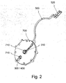
- Fig. 2 shows two contact devices according to the invention arranged in a shaped body.
- FIG. 3 shows a detailed representation of a contact device according to the invention.
- the power semiconductor components (600) in pressure-contacted power semiconductor modules (800) and disc cells are connected on both sides with a flat metal body (650) whose coefficient of thermal expansion between the coefficient of thermal expansion of horaumaleiterbauelements (600) and the coefficient of thermal expansion of a subsequent contactor (812) is the power terminals to reduce the thermal stress for the stress semiconductor device (600).
- the connection of the power semiconductor component (600) with the flat metal bodies (650), which preferably consist of molybdenum, can be realized by different methods, for example by soldering, gluing or pressure contacting of the two partners.
- the sheet metal body (650) typically has a thickness of the order of a few tenths to a few millimeters.
- the contact device (400) is here an assembly for the assembly of the power semiconductor module (800), which is arranged in the molded body (700) and thus a simple mounting of the power semiconductor module (800) is accessible.
- two contact devices (400) are used for this purpose in the associated molded body (700).
- These moldings (700) are formed from a thermosetting plastic, since they are used only for the pressure introduction via the pressure contact device (808) but not the electrical connection, since the power terminals (812) are designed here as metallic terminal lugs.
- the electrical connection of the contact device (400) to the outside is formed in each case by means of a cable (500) with a connector (520) connected thereto.
- the cable (500) is connected to the contact device (400), preferably by means of a crimp connection (220, 510).
- the plastic housing (300) of the contact device (400) additionally serves for the electrical isolation of the control signal from the power connection, which is formed by the metallic molded body (812).
- FIG. 2 shows two contact devices (400) according to the invention arranged in a molded body (700) as a detail of FIG. 1. Shown is the molded body (700) of a preferably duroplastic plastic with two recesses (710) for each contact device (400). Each contact device (400) has a plastic housing (300), wherein a recess (310) is provided on the side facing the power semiconductor component (600, see FIG. Through this recess (310) protrudes the pin-like extension (110) of the contact spring (100, see Fig. 3).
- This pin-like extension (110) is used in the centrally arranged contact device (400) contacting the control terminal (610) of the power semiconductor device (600).
- the contact device (400) for contacting the Steueranschtusses partially through a recess (650, 814, see Fig. 1) at least one disposed between the power semiconductor device and the molded body sheet metal molding (650 812, see FIG.
- the pin-like extension (110) with the control contact surface (610) of the power semiconductor device (600) is electrically connected.
- the non-centrally arranged contact device (400) is used for auxiliary contact of the power semiconductor device (600), as it is known for example as an auxiliary emitter.
- a further contact device (400) designed identically to the centrally arranged contact device (400) is likewise arranged in the molded body (700).
- the associated recess (710) is formed deeper, so that the pin-like extension (110) of the contact device (400) for contacting the auxiliary terminal with the arranged between the power semiconductor device (600) and the molding (700) flat metal moldings (650) or a Power connection element (812) is electrically connected.
- connecting cables (500) starting from the contact devices (400) to a respective plug (520) which forms the associated external connections of the power semiconductor module (800).
- Fig. 3 shows a detailed view of a contact device (400) according to the invention on the one hand as an exploded view as well as in section.
- This contact device (400) consists of a multi-part, here two-part, insulating housing (300), a contact spring (100) and a metal shaped body (200).
- the contact spring (100) itself is designed as a helical spring with a pin-like extension (110) at the first spring end. This extension (110) serves to make contact, for example, with the control connection (610) of the power semiconductor component (600).
- the resilient portion of the contact spring (100) is used over the life of the disk cell or the power semiconductor module (800) constant pressure introduction and thus secure contacting of the control terminal (610).
- the second spring end is used for electrical contact with the metal molding (200).
- This metal shaped body (200) has, as first connecting device (210) to the contact spring (100), a first planar section arranged parallel to the power semiconductor component (600). Likewise, it has a second connection device (220) for connection to a connecting cable (500). This connecting device (220) of the metal molding (200) is formed as a crimped connection to the connection cable (500).
- the insulating housing (300) is designed in two pieces, wherein the upper part (304) partially protrudes into the lower part (302) and thus the two parts are fixed relative to one another.
- a snap-locking connection may be provided between the two parts.
- the lower part (302) of the insulating material housing (300) has on its side facing the power semiconductor component (600, cf., FIGS. 1 and 2) a recess (310) as lead-through for the pin-like extension (110) of the contact spring (100).
- the upper part (304) of the insulating housing (300) has a lateral recess (320) for passing through the connecting device (220) of the metal shaped body (200).
Landscapes
- Die Bonding (AREA)
- Connector Housings Or Holding Contact Members (AREA)
- Inverter Devices (AREA)
- Details Of Connecting Devices For Male And Female Coupling (AREA)
- Connecting Device With Holders (AREA)
Abstract
Description
- Es wird eine Anordnung mit einer Kontakteinrichtung für den Steueranschluss eines Leistungshalbleiterbauelements in Scheibenzellen und Leistungshalbleitermodulen beschrieben. Eine derartige Kontakteinrichtungen ist beispielhaft aus der
DE 10 2004 058 946 A1 undDE 10 2004 050 588 bekannt. - Erstgenannte Druckschrift offenbart eine Scheibenzelle mit einem Steueranschluss zum Steuerkontakt des Leistungshalbleiterbauelements, wobei der Steueranschluss ausgebildet ist als ein Drahtelement welches im Bereich des Leistungshalbleiterbauelements in einer Kunststoffhülse geführt ist. Diese Kunststoffhülse und somit die Kontaktfläche des Drahtes zum Steuerkontakt wird mittels einer Feder in Richtung des Leistungshalbleiterbauelements gedrückt. Eine derartige Ausgestaltung gemäß dem Stand der Technik ist einer rationellen Fertigung mit einer möglichst geringen Anzahl von einzelnen vorgefertigten Baugruppen nicht zugänglich.
- Zweitgenannte Druckschrift offenbart eine Anordnung mit einem Leistungshalbleiterbauelement in einem Leistungshalbleitermodul oder einer Scheibenzelle, wobei oberhalb des Leistungshalbleiterbauelements ein Formkörper angeordnet ist, der im Bereich des Steueranschlusses eine Ausnehmung mit einem Widerlager aufweist. Die Kontakteinrichtung selbst besteht aus einer Kontaktfeder mit einem stiftartigen Fortsatz an demjenigen Federende, das den Steueranschluss kontaktiert, und weiterhin mit einer mittels eines Metallformteils gebildeten Verbindung mit einem Anschlusskabel zur externen Verbindung am anderen Federende. Die Kontakteinrichtung weist hierzu eine Isolierstoffhülse mit darin angeordneter Kontaktfeder auf, wobei die Isolierstoffhülse weiterhin Rastnasen aufweist, die zusammen mit einem Widerlager des Formkörpers eine Schnapp- Rast- Verbindung bilden. Nachteilig an dieser Ausgestaltung der Kontakteinrichtung ist, dass sie ein große Bauhöhe aufweist und daher in manchen kompakten Leistungshalbleitermodulen oder Scheibenzellen nicht anordenbar ist.
- Der Erfindung liegt die Aufgabe zugrunde eine Anordnung mit einer Kontakteinrichtung für einen Steuer- und /oder Hilfsanschluss von Leistungshalbleiterbauelementen in Scheibenzellen und Leistungshalbleitermodulen vorzustellen, die kompakt und universell einsetzbar ist, einen dauerhaft sicheren elektrischen Kontakt gewährleistet und einer einfachen Montage in Form einer Baugruppe zugänglich ist.
- Die Aufgabe wird erfindungsgemäß gelöst, durch eine Anordnung mit den Merkmalen des Anspruchs 1. Bevorzugte Ausführungsformen sind in den Unteransprüchen beschrieben.
- Der Grundgedanke der Erfindung geht aus von einem Leistungshalbleitermodul, vorzugsweise in Druckkontaktierung mit einem oder mehreren Leistungshalbleiterbauelementen oder einer Scheibenzelle. In einer Scheibenzelle ist typischerweise nur ein Leistungshalbleiterbauelement angeordnet, allerdings gibt es Sonderformen mit einer Mehrzahl von Leistungshalbleiterbauelementen in einem Gehäuse.
- Die Erfindung bezieht sich auf Leistungshalbleitermodule oder auf Scheibenzellen mit mindestens einem gesteuerten Leistungshalbleiterbauelement, wie einem Thyristor oder einem Transistor. Diese weisen pro gesteuertem Leistungshalbleiterbauelement einen Steueranschluss und meist auch mindestens einen Hilfsanschluss auf, die jeweils mit einer externen Kontakteinrichtung verbunden sind.
- Die erfindungsgemäße Anordnung mit einem Leistungshalbleiterbauelement in einem Leistungshalbleitermodul oder einer Scheibenzelle weist hierbei oberhalb des Leistungshalbleiterbauelements einen Formkörper mit mindestens einer Ausnehmung auf. Mindestens eine Kontakteinrichtung zur Hilfs- oder Steueranschlusskontaktierung des Leistungshalbleiterbauelements ist zur Anordnung in einer derartigen Ausnehmung vorgesehen.
- Die Kontakteinrichtung selbst besteht aus einer Kontaktfeder mit einem stiftartigen Fortsatz an demjenigen ersten Federende, das dem Leistungshalbleiterbauelement zugewandt ist. An dem zweiten Federende ist ein Metallformkörper vorgesehen mit einer ersten Verbindungseinrichtung ausgestaltet als flächiger Abschnitt des Metallformkörpers parallel angeordnet zum Leistungshalbleiterbauelement und mit einer zweiten Verbindungseinrichtung zur Verbindung mit einem Anschlusskabel. Weiterhin weist die Kontakteinrichtung ein mehrteiliges Isolierstoffgehäuse zur Anordnung der Kontaktfeder und des Metallformkörpers, auf. Hierzu weist dieses Isolierstoffgehäuse eine erste Ausnehmung für den stiftartigen Fortsatz und eine zweite seitlich angeordnete Ausnehmung für die zweite Verbindungseinrichtung auf.
- Der erfinderische Gedanke wird anhand der Ausführungsbeispiele in den Fig. 1 bis 3 näher erläutert.
- Fig. 1 zeigt eine dreidimensionale Explosionsdarstellung eines Leistungshalbleitermoduls mit einer erfindungsgemäßen Kontakteinrichtung.
- Fig. 2 zeigt zwei erfindungsgemäße Kontakteinrichtungen angeordnet in einem Formkörper.
- Fig. 3 zeigt eine Detaildarstellung einer erfindungsgemäßen Kontakteinrichtung.
- Fig. 1 zeigt eine dreidimensionale Explosionsdarstellung einer erfindungsgemäßen Anordnung in Ausgestaltung eines Leistungshalbleitermoduls (800) mit einer Kontakteinrichtung (400). Dargestellt ist ein Leistungshalbleitermodul (800) mit zwei Thyristoren (600) aufgebaut in Druckkontakttechnik. Auf einer Grundplatte (802) sind in geeigneter Weise angeordnet:
- Isolationsmaterial zur elektrischen Isolation der Strom führenden Teile des Leistungshalbleitermoduls (800) von der Grundplatte (802);
- die beiden Thyristoren (600) mit geeigneten elektrischen Lastverbindungselementen (812);
- zwei Formkörper (700) zur Aufnahme der Kontakteinrichtungen und zur Einleitung des Drucks auf die Leistungshalbleiterbauelemente
- eine Druckkontakteinrichtung (808) und
- ein Gehäuse (804) mit Deckel (810).
- Häufig werden die Leistungshalbleiterbauelemente (600) in druckkontaktierten Leistungshalbleitermodulen (800) und Scheibenzellen beidseitig mit je einem flächigen Metallkörper (650) verbunden, dessen Wärmeausdehnungskoeffizient zwischen dem Wärmeausdehnungskoeffizienten des Leistungshalfaleiterbauelements (600) und dem Wärmeausdehnungskoeffizienten einer anschließenden Kontakteinrichtung (812) der Leistungsanschlüsse liegt, um den thermischen Stress für das Leisfungshalbleiterbauelement (600) zu verringern. Die Verbindung des Leistungshalbleiterbauelements (600) mit den flächigen Metallkörpern (650), die vorzugsweise aus Molybdän bestehen, kann durch unterschiedliche Verfahren realisiert werden, beispielhaft durch Verlöten, Verkleben oder Druckkontaktierung der beiden Partner. Der flächige Metallkörper (650) weist typischerweise eine Dicke in der Größenordnung von einigen zehntel bis einigen Millimetern auf.
- Die Kontakteinrichtung (400) ist hier eine Baugruppe für den Zusammenbau des Leistungshalbleitermoduls (800), die in den Formkörper (700) angeordnet ist und somit einer einfachen Montage des Leistungshalbleitermoduls (800) zugänglich ist. Jeweils zwei Kontakteinrichtungen (400) werden hierzu in die zugeordneten Formkörper (700) eingesetzt. Diese Formkörper (700) sind aus einem duroplasten Kunststoff gebildet, da sie nur der Druckeinleitung über die Druckkontakteinrichtung (808) nicht aber der elektrischen Verbindung dienen, da die Leistungsanschlüsse (812) hier als metallische Anschlusslaschen ausgeführt sind. Die elektrische Verbindung der Kontakteinrichtung (400) nach außen wird jeweils mittels eines Kabels (500) mit einem damit verbundener Stecker (520) gebildet. Das Kabel (500) ist mit der Kontakteinrichtung (400) vorzugsweise mittels einer Crimpverbindung (220, 510) verbunden.
- Das Kunststoffgehäuse (300) der Kontakteinrichtung (400) dient zusätzlich der elektrischen Isolation beispielhaft des Steuersignals vom Leistungsanschluss, der durch den metallischen Formkörper (812) gebildet wird.
- Fig. 2 zeigt zwei erfindungsgemäße Kontakteinrichtungen (400) angeordnet in einem Formkörper (700) als Detaildarstellung der Fig. 1. Dargestellt ist der Formkörper (700) aus einem vorzugsweise duroplasten Kunststoff mit zwei Ausnehmungen (710) für jeweils eine Kontakteinrichtung (400). Jede Kontakteinrichtung (400) weist ein Kunststoffgehäuse (300) auf, wobei auf der dem Leistungshalbleiterbauelement (600, vgl. Fig. 1) zugewandten Seite eine Ausnehmung (310) vorgesehen ist. Durch diese Ausnehmung (310) ragt der stiftartige Fortsatz (110) der Kontaktfeder (100, vgl. Fig. 3).
- Dieser stiftartige Fortsatz (110) dient bei der zentral angeordneten Kontakteinrichtung (400) der Kontaktierung des Steueranschlusses (610) des Leistungshalbleiterbauelements(600). Hierzu reicht die Kontakteinrichtung (400) zur Kontaktierung des Steueranschtusses teilweise durch eine Ausnehmung (650, 814, vgl. Fig. 1) mindestens eines zwischen dem Leistungshalbleiterbauelement und dem Formkörper angeordneten flächigen Metallformkörper (650 812, vgl. Fig. 1) hindurch. Somit ist der stiftartige Fortsatz (110) mit der Steuerkontaktfläche (610) des Leistungshalbleiterbauelements (600) elektrisch leitend verbunden.
- Die nicht zentral angeordnete Kontakteinrichtung (400) dient der Hilfskontaktierung des Leistungshalbleiterbauelements (600), wie sie beispielhaft als Hilfsemitter bekannt ist. Hierzu ist eine identisch zur zentral angeordneten Kontakteinrichtung (400) ausgebildete weitere Kontakteinrichtung (400) ebenfalls in dem Formkörper (700) angeordnet. Allerdings ist die zugeordnete Ausnehmung (710) tiefer ausgebildet, so dass der stiftartige Fortsatz (110) der Kontakteinrichtung (400) zur Kontaktierung des Hilfsanschlusses mit dem zwischen dem Leistungshalbleiterbauelement (600) und dem Formkörper (700) angeordneten flächigen Metallformkörper (650) oder einem Leistungsanschlusselement (812) elektrisch leitend verbunden ist.
- Ebenfalls dargestellt sind Anschlusskabel (500) ausgehend von den Kontakteinrichtungen (400) zu jeweils einem Stecker (520), der die zugeordneten externen Anschlüsse des Leistungshalbleitermoduls (800) ausbildet.
- Fig. 3 zeigt eine Detaildarstellung einer erfindungsgemäßen Kontakteinrichtung (400) einerseits als Explosionsdarstellung wie auch im Schnitt. Diese Kontakteinrichtung (400) besteht aus einem mehrteiligen, hier zweiteiligen, Isolierstoffgehäuse (300), einer Kontaktfeder (100) und einem Metallformkörper (200).
- Die Kontaktfeder (100) selbst ist als Schraubenfeder mit einem stiftartigen Fortsatz (110) am ersten Federende ausgebildet. Dieser Fortsatz (110) dient der Kontaktierung beispielhaft des Steueranschlusses (610) des Leistungshalbleiterbauelements (600). Der federnde Abschnitt der Kontaktfeder (100) dient der über die Lebensdauer der Scheibenzelle bzw. des Leistungshalbleitermoduls (800) konstanten Druckeinleitung und damit sicheren Kontaktierung des Steueranschlusses (610). Das zweite Federende dient dem elektrischen Kontakt zum Metallformkörper (200).
- Dieser Metallformkörper (200) weist als erste Verbindungseinrichtung (210) zur Kontaktfeder (100) einen ersten flächigen Abschnitt parallel angeordnet zum Leistungshalbleiterbauelement (600) auf. Ebenso weist er eine zweite Verbindungseinrichtung (220) zur Verbindung mit einem Anschlusskabel (500) auf. Diese Verbindungseinrichtung (220) des Metallformkörpers (200) ist als Crimpverbindung zu dem Anschlusskabel (500), ausgebildet.
- Das Isolierstoffgehäuse (300) ist zweistückig ausgestaltet wobei der obere Teil (304) in den unteren Teil (302) teilweise hineinragt und somit die beiden Teile zueinander fixiert sind. Alternativ kann eine nicht dargestellte Schnapp- Rast- Verbindung zwischen den beiden Teilen vorgesehen werden. Durch die Verbindung der beiden Teile (302, 304) wird ein flächiger Abschnitt, die erste Verbindungseinrichtung (210), des Metallformkörper (200) auf das zweite Federende gepresst, gleichzeitig die Feder (100) selbst mäßig gespannt.
- Der untere Teil (302) des Isolierstoffgehäuses (300) weist auf seiner dem Leistungshalbleiterbauelement (600, vgl. Fig. 1 und 2) zugewandten Seite eine Ausnehmung (310) als Durchführung für den stiftartigen Fortsatz (110) der Kontaktfeder (100) auf. Der obere Teil (304) des Isolierstoffgehäuses (300) weist eine seitliche Ausnehmung (320) zur Durchführung der Verbindungseinrichtung (220) des Metallformkörpers (200) auf.
Claims (7)
- Anordnung mit einem Leistungshalbleiterbauelement (600) in einem Leistungshalbleitermodul (800) oder einer Scheibenzelle, wobei oberhalb des Leistungshalbleiterbauelements (600) ein Formkörper (700) angeordnet ist, der mindestens eine Ausnehmung (710, 720) aufweist,
mit mindestens einer Kontakteinrichtung (400) zur Hilfs- oder
Steueranschlusskontaktierung des Leistungshalbleiterbauelements (600), wobei die Kontakteinrichtung (400) zur Anordnung in einer Ausnehmung (710, 720) vorgesehen ist und besteht
aus einer Kontaktfeder (100) mit einem stiftartigen Fortsatz (1'10) an demjenigen ersten Federende, das dem Leistungshalbleiterbauelement (600) zugewandt ist, und mit einem an dem zweiten Federende angeordneten Metallformkörper (200) mit einer ersten Verbindungseinrichtung (210) ausgestaltet als flächiger Abschnitt des
Metallformkörpers (200) parallel angeordnet zum Leistungshalbleiterbauelement (600) und mit einer zweiten Verbindungseinrichtung (220) zur Verbindung mit einem Anschlusskabel (500) und
aus einem mehrteiligen Isolierstoffgehäuse (300) zur Anordnung der Kontaktfeder (100) und des Metallformkörpers (200), wobei dieses Isolierstoffgehäuse (300) eine erste Ausnehmung (310) für den stiftartigen Fortsatz (110) und eine zweite seitlich angeordnete Ausnehmung (320) für die zweite Verbindungseinrichtung (220) aufweist. - Anordnung nach Anspruch 1,
wobei das Isolierstoffgehäuse (300) zweistückig ausgebildet ist und die beiden Teile (302, 304) über eine Schnapp- Rast- Verbindung zueinander angeordnet sind. - Anordnung nach Anspruch 1,
wobei das lsolierstoffgehäuse (300) zweistückig ausgebildet ist und die beiden Teile (302, 304) ineinander angeordnet sind und hierdurch der Metallformkörper (200) auf das zweite Federende gepresst wird und die Feder (100) selbst leicht gespannt wird. - Anordnung nach Anspruch 1,
wobei die Kontaktfeder (100) als Schraubenfeder ausgebildet ist. - Anordnung nach Anspruch 1,
wobei die zweite Verbindungseinrichtung (220) des Metallformkörpers (200) als Crimpverbindung zu dem Anschlusskabel (500), ausgebildet ist. - Anordnung nach Anspruch 1,
wobei die Kontakteinrichtung (400) zur Kontaktierung des Steueranschlusses teilweise durch mindestens eine Ausnehmung (652, 814) mindestens eines zwischen dem Leistungshalbleiterbauelement (600) und dem Formkörper (700) angeordneten flächigen Metallformkörpers (650, 812) hindurch reicht und hierbei der stiftartige Fortsatz (110) mit der Steuerkontaktfläche (610) des Leistungshalbleiterbauelements (600) elektrisch leitend verbunden ist. - Anordnung nach Anspruch 1,
wobei der stiftartige Fortsatz (110) der Kontaktfeder (100) der Kontakteinrichtung (400) zur Kontaktierung des Hilfsanschlusses mit dem zwischen dem Leistungshalbleiterbauelement (600) und dem Formkörper (700) angeordneten flächigen Metallformkörpers (650, 812) elektrisch leitend verbunden ist.
Applications Claiming Priority (1)
| Application Number | Priority Date | Filing Date | Title |
|---|---|---|---|
| DE102006034964A DE102006034964B3 (de) | 2006-07-28 | 2006-07-28 | Anordnung mit einem Leistungshalbleiterbauelement und mit einer Kontakteinrichtung |
Publications (3)
| Publication Number | Publication Date |
|---|---|
| EP1883108A2 true EP1883108A2 (de) | 2008-01-30 |
| EP1883108A3 EP1883108A3 (de) | 2008-07-02 |
| EP1883108B1 EP1883108B1 (de) | 2013-09-11 |
Family
ID=38329557
Family Applications (1)
| Application Number | Title | Priority Date | Filing Date |
|---|---|---|---|
| EP07013421.8A Active EP1883108B1 (de) | 2006-07-28 | 2007-07-10 | Anordnung mit einem Leistungshalbleiterbauelement und einer Kontakteinrichtung |
Country Status (6)
| Country | Link |
|---|---|
| US (1) | US7705442B2 (de) |
| EP (1) | EP1883108B1 (de) |
| JP (1) | JP5238198B2 (de) |
| KR (1) | KR101343274B1 (de) |
| CN (1) | CN101114641B (de) |
| DE (1) | DE102006034964B3 (de) |
Families Citing this family (8)
| Publication number | Priority date | Publication date | Assignee | Title |
|---|---|---|---|---|
| DE102006034964B3 (de) * | 2006-07-28 | 2007-09-06 | Semikron Elektronik Gmbh & Co. Kg | Anordnung mit einem Leistungshalbleiterbauelement und mit einer Kontakteinrichtung |
| DE102009022660B3 (de) | 2009-05-26 | 2010-09-16 | Semikron Elektronik Gmbh & Co. Kg | Befestigung eines Bauelements an einem Substrat und/oder eines Anschlusselementes an dem Bauelement und/oder an dem Substrat durch Drucksinterung |
| DE102009024421B3 (de) | 2009-06-09 | 2010-07-08 | Semikron Elektronik Gmbh & Co. Kg | Steueranschlusskontakteinrichtung für ein Leistungshalbleiterbauelement |
| DE102010000694B4 (de) * | 2009-12-18 | 2013-12-12 | Semikron Elektronik Gmbh & Co. Kg | Leistungshalbleitermodul mit Druckkontaktfedern |
| DE102010041892A1 (de) | 2010-10-01 | 2012-04-05 | Semikron Elektronik Gmbh & Co. Kg | Leistungshalbleitermodul mit einem Grundmodul und einem Verbindungsmodul |
| DE102010041849A1 (de) | 2010-10-01 | 2012-04-05 | Semikron Elektronik Gmbh & Co. Kg | Leistungshalbleitermodul mit einem Grundmodul und einem Verbindungsmodul |
| DE102011076324B4 (de) * | 2011-05-24 | 2014-04-10 | Semikron Elektronik Gmbh & Co. Kg | Leistungselektronisches System mit Verbindungseinrichtung erster und zweiter Subsysteme |
| DE102024127418A1 (de) * | 2024-09-23 | 2026-03-26 | Infineon Technologies Bipolar Gmbh & Co. Kg | Halbleitermodul |
Citations (3)
| Publication number | Priority date | Publication date | Assignee | Title |
|---|---|---|---|---|
| DE10254617A1 (de) | 2002-03-28 | 2003-10-30 | Mitsubishi Electric Corp | Halbleitervorrichtung |
| DE102004050588A1 (de) | 2004-10-16 | 2006-04-20 | Semikron Elektronik Gmbh & Co. Kg | Kontakteinrichtung für Leistungshalbleitermodule und Scheibenzellen |
| DE102004058946A1 (de) | 2004-12-08 | 2006-06-14 | Semikron Elektronik Gmbh & Co. Kg | Leistungshalbleitermodul mit Hilfsanschluss |
Family Cites Families (13)
| Publication number | Priority date | Publication date | Assignee | Title |
|---|---|---|---|---|
| DE3826820A1 (de) * | 1987-09-28 | 1989-04-06 | Asea Brown Boveri | Leistungshalbleiterelement |
| WO1993023825A1 (fr) * | 1992-05-20 | 1993-11-25 | Seiko Epson Corporation | Cartouche destinee a un appareil electronique |
| US5451165A (en) * | 1994-07-27 | 1995-09-19 | Minnesota Mining And Manufacturing Company | Temporary package for bare die test and burn-in |
| JP3533317B2 (ja) * | 1997-08-28 | 2004-05-31 | 株式会社東芝 | 圧接型半導体装置 |
| US5990549A (en) * | 1998-02-06 | 1999-11-23 | Intel Corporation | Thermal bus bar design for an electronic cartridge |
| US5940273A (en) * | 1998-06-08 | 1999-08-17 | Inductotherm Corp. | Semiconductor clamping device |
| US6107711A (en) * | 1998-08-21 | 2000-08-22 | Emerson Electric Co. | Brushless exciter for a rotating electromagnetic machine |
| US6504445B1 (en) * | 2001-12-07 | 2003-01-07 | Renaissance Electronics Corporation | Surface mountable low IMD circulator/isolator with a locking cover and assembly method |
| EP1579004B1 (de) | 2002-10-23 | 2010-06-16 | VIRxSYS Corporation | Screening-verfahren zur identifizierung wirksamer prä-trans-spleissmoleküle |
| US7264481B2 (en) * | 2003-08-22 | 2007-09-04 | Abb Schweiz Ag | Pressure contract spring for contact arrangement in power semiconductor module |
| DE102004057421B4 (de) * | 2004-11-27 | 2009-07-09 | Semikron Elektronik Gmbh & Co. Kg | Druckkontaktiertes Leistungshalbleitermodul für hohe Umgebungstemperaturen und Verfahren zu seiner Herstellung |
| DE102006034964B3 (de) * | 2006-07-28 | 2007-09-06 | Semikron Elektronik Gmbh & Co. Kg | Anordnung mit einem Leistungshalbleiterbauelement und mit einer Kontakteinrichtung |
| CN200941348Y (zh) * | 2006-08-18 | 2007-08-29 | 富士康(昆山)电脑接插件有限公司 | 开关 |
-
2006
- 2006-07-28 DE DE102006034964A patent/DE102006034964B3/de active Active
-
2007
- 2007-07-10 EP EP07013421.8A patent/EP1883108B1/de active Active
- 2007-07-25 JP JP2007193318A patent/JP5238198B2/ja active Active
- 2007-07-27 CN CN2007101367605A patent/CN101114641B/zh active Active
- 2007-07-27 KR KR1020070075587A patent/KR101343274B1/ko active Active
- 2007-07-30 US US11/881,966 patent/US7705442B2/en active Active
Patent Citations (3)
| Publication number | Priority date | Publication date | Assignee | Title |
|---|---|---|---|---|
| DE10254617A1 (de) | 2002-03-28 | 2003-10-30 | Mitsubishi Electric Corp | Halbleitervorrichtung |
| DE102004050588A1 (de) | 2004-10-16 | 2006-04-20 | Semikron Elektronik Gmbh & Co. Kg | Kontakteinrichtung für Leistungshalbleitermodule und Scheibenzellen |
| DE102004058946A1 (de) | 2004-12-08 | 2006-06-14 | Semikron Elektronik Gmbh & Co. Kg | Leistungshalbleitermodul mit Hilfsanschluss |
Also Published As
| Publication number | Publication date |
|---|---|
| KR20080011113A (ko) | 2008-01-31 |
| DE102006034964B3 (de) | 2007-09-06 |
| EP1883108B1 (de) | 2013-09-11 |
| CN101114641B (zh) | 2011-03-09 |
| JP2008034847A (ja) | 2008-02-14 |
| EP1883108A3 (de) | 2008-07-02 |
| JP5238198B2 (ja) | 2013-07-17 |
| US7705442B2 (en) | 2010-04-27 |
| CN101114641A (zh) | 2008-01-30 |
| KR101343274B1 (ko) | 2013-12-18 |
| US20080023818A1 (en) | 2008-01-31 |
Similar Documents
| Publication | Publication Date | Title |
|---|---|---|
| EP1883108B1 (de) | Anordnung mit einem Leistungshalbleiterbauelement und einer Kontakteinrichtung | |
| EP1777720B1 (de) | Elektrisches Bauteil, insbesondere Relaisfassung, mit Federklemmen und Verfahren zu seiner Herstellung | |
| DE102009055882B4 (de) | Leistungshalbleitervorrichtung | |
| DE102004050588B4 (de) | Anordnung mit einem Leistungshalbleiterbauelement und mit einer Kontakteinrichtung | |
| DE102011013449B4 (de) | Baugruppe mit einem Träger, einem SMD-Bauteil und einem Stanzgitterteil | |
| EP3262666A1 (de) | Elektrisches bauelement und verfahren zur herstellung eines elektrischen bauelements | |
| DE102007043197A1 (de) | Anschlussklemme | |
| EP1840961A2 (de) | Leistungshalbleitermodul und zugehöriges Herstellungsverfahren | |
| EP1933380B1 (de) | Leistungshalbleitermodul mit Kontaktfedern | |
| EP2933890A1 (de) | Unterputzeinsatz eines elektrischen Installationsgerätes | |
| EP2305010B1 (de) | Elektrische schaltungsanordnung | |
| EP2854238B1 (de) | Hochfrequenz-Abdichtung von Hochfrequenz-Steckverbindern | |
| DE102011108937A1 (de) | Hochstromkontaktelement für Leiterplatten | |
| EP1791178B1 (de) | Leistungshalbleitermodul in Druckkontaktausführung | |
| EP2673848B1 (de) | Steckverbindung zur elektrischen direktkontaktierung einer leiterplatte | |
| DE102023210385A1 (de) | Kontaktvorrichtung und Leistungsmodulanordnung | |
| EP2048740A1 (de) | Elektrische Steckverbindung mit einem Klemmelement | |
| EP3304651B1 (de) | Elektrischer steckverbinder | |
| WO2013017473A2 (de) | Elektronikanordnung | |
| EP1758214A1 (de) | Anordnung mit Leistungshalbleitermodul und mit Anschlussverbinder | |
| DE102023210379A1 (de) | Kontaktvorrichtung und Leistungsmodulanordnung | |
| DE19639723A1 (de) | Elektrischer Verbinder mit einem Kurzschlußkontakt und Kurzschlußkontakt | |
| WO2022242987A1 (de) | Elektrische anordnung mit drosselspule | |
| DE102011009440A1 (de) | Vorrichtung zur elektronischen und mechanischen Verbindung von zwei nebeneinander angeordneten Leiterplatten | |
| DE102019134369A1 (de) | Leadframe für Drahtbauteile mit Kulissenstruktur |
Legal Events
| Date | Code | Title | Description |
|---|---|---|---|
| PUAI | Public reference made under article 153(3) epc to a published international application that has entered the european phase |
Free format text: ORIGINAL CODE: 0009012 |
|
| AK | Designated contracting states |
Kind code of ref document: A2 Designated state(s): AT BE BG CH CY CZ DE DK EE ES FI FR GB GR HU IE IS IT LI LT LU LV MC MT NL PL PT RO SE SI SK TR |
|
| AX | Request for extension of the european patent |
Extension state: AL BA HR MK YU |
|
| RIN1 | Information on inventor provided before grant (corrected) |
Inventor name: SCHLOETTERER, ANDRE |
|
| PUAL | Search report despatched |
Free format text: ORIGINAL CODE: 0009013 |
|
| AK | Designated contracting states |
Kind code of ref document: A3 Designated state(s): AT BE BG CH CY CZ DE DK EE ES FI FR GB GR HU IE IS IT LI LT LU LV MC MT NL PL PT RO SE SI SK TR |
|
| AX | Request for extension of the european patent |
Extension state: AL BA HR MK RS |
|
| 17P | Request for examination filed |
Effective date: 20080619 |
|
| 17Q | First examination report despatched |
Effective date: 20080820 |
|
| AKX | Designation fees paid |
Designated state(s): AT BE BG CH CY CZ DE DK EE ES FI FR GB GR HU IE IS IT LI LT LU LV MC MT NL PL PT RO SE SI SK TR |
|
| GRAP | Despatch of communication of intention to grant a patent |
Free format text: ORIGINAL CODE: EPIDOSNIGR1 |
|
| RIC1 | Information provided on ipc code assigned before grant |
Ipc: H01L 23/00 20060101ALI20130425BHEP Ipc: H01L 25/07 20060101ALI20130425BHEP Ipc: H01L 23/48 20060101AFI20130425BHEP |
|
| INTG | Intention to grant announced |
Effective date: 20130523 |
|
| GRAS | Grant fee paid |
Free format text: ORIGINAL CODE: EPIDOSNIGR3 |
|
| GRAA | (expected) grant |
Free format text: ORIGINAL CODE: 0009210 |
|
| AK | Designated contracting states |
Kind code of ref document: B1 Designated state(s): AT BE BG CH CY CZ DE DK EE ES FI FR GB GR HU IE IS IT LI LT LU LV MC MT NL PL PT RO SE SI SK TR |
|
| REG | Reference to a national code |
Ref country code: GB Ref legal event code: FG4D Free format text: NOT ENGLISH |
|
| REG | Reference to a national code |
Ref country code: CH Ref legal event code: EP |
|
| REG | Reference to a national code |
Ref country code: AT Ref legal event code: REF Ref document number: 632046 Country of ref document: AT Kind code of ref document: T Effective date: 20130915 |
|
| REG | Reference to a national code |
Ref country code: IE Ref legal event code: FG4D Free format text: LANGUAGE OF EP DOCUMENT: GERMAN |
|
| REG | Reference to a national code |
Ref country code: CH Ref legal event code: NV Representative=s name: BRAUNPAT BRAUN EDER AG, CH |
|
| REG | Reference to a national code |
Ref country code: DE Ref legal event code: R096 Ref document number: 502007012256 Country of ref document: DE Effective date: 20131107 |
|
| PG25 | Lapsed in a contracting state [announced via postgrant information from national office to epo] |
Ref country code: SE Free format text: LAPSE BECAUSE OF FAILURE TO SUBMIT A TRANSLATION OF THE DESCRIPTION OR TO PAY THE FEE WITHIN THE PRESCRIBED TIME-LIMIT Effective date: 20130911 Ref country code: LT Free format text: LAPSE BECAUSE OF FAILURE TO SUBMIT A TRANSLATION OF THE DESCRIPTION OR TO PAY THE FEE WITHIN THE PRESCRIBED TIME-LIMIT Effective date: 20130911 Ref country code: CY Free format text: LAPSE BECAUSE OF FAILURE TO SUBMIT A TRANSLATION OF THE DESCRIPTION OR TO PAY THE FEE WITHIN THE PRESCRIBED TIME-LIMIT Effective date: 20130703 |
|
| REG | Reference to a national code |
Ref country code: NL Ref legal event code: VDEP Effective date: 20130911 |
|
| REG | Reference to a national code |
Ref country code: LT Ref legal event code: MG4D |
|
| PG25 | Lapsed in a contracting state [announced via postgrant information from national office to epo] |
Ref country code: SI Free format text: LAPSE BECAUSE OF FAILURE TO SUBMIT A TRANSLATION OF THE DESCRIPTION OR TO PAY THE FEE WITHIN THE PRESCRIBED TIME-LIMIT Effective date: 20130911 Ref country code: ES Free format text: LAPSE BECAUSE OF FAILURE TO SUBMIT A TRANSLATION OF THE DESCRIPTION OR TO PAY THE FEE WITHIN THE PRESCRIBED TIME-LIMIT Effective date: 20130911 Ref country code: LV Free format text: LAPSE BECAUSE OF FAILURE TO SUBMIT A TRANSLATION OF THE DESCRIPTION OR TO PAY THE FEE WITHIN THE PRESCRIBED TIME-LIMIT Effective date: 20130911 Ref country code: GR Free format text: LAPSE BECAUSE OF FAILURE TO SUBMIT A TRANSLATION OF THE DESCRIPTION OR TO PAY THE FEE WITHIN THE PRESCRIBED TIME-LIMIT Effective date: 20131212 Ref country code: FI Free format text: LAPSE BECAUSE OF FAILURE TO SUBMIT A TRANSLATION OF THE DESCRIPTION OR TO PAY THE FEE WITHIN THE PRESCRIBED TIME-LIMIT Effective date: 20130911 |
|
| REG | Reference to a national code |
Ref country code: SK Ref legal event code: T3 Ref document number: E 15376 Country of ref document: SK |
|
| PG25 | Lapsed in a contracting state [announced via postgrant information from national office to epo] |
Ref country code: CY Free format text: LAPSE BECAUSE OF FAILURE TO SUBMIT A TRANSLATION OF THE DESCRIPTION OR TO PAY THE FEE WITHIN THE PRESCRIBED TIME-LIMIT Effective date: 20130911 |
|
| PG25 | Lapsed in a contracting state [announced via postgrant information from national office to epo] |
Ref country code: CZ Free format text: LAPSE BECAUSE OF FAILURE TO SUBMIT A TRANSLATION OF THE DESCRIPTION OR TO PAY THE FEE WITHIN THE PRESCRIBED TIME-LIMIT Effective date: 20130911 Ref country code: IS Free format text: LAPSE BECAUSE OF FAILURE TO SUBMIT A TRANSLATION OF THE DESCRIPTION OR TO PAY THE FEE WITHIN THE PRESCRIBED TIME-LIMIT Effective date: 20140111 Ref country code: RO Free format text: LAPSE BECAUSE OF FAILURE TO SUBMIT A TRANSLATION OF THE DESCRIPTION OR TO PAY THE FEE WITHIN THE PRESCRIBED TIME-LIMIT Effective date: 20130911 Ref country code: NL Free format text: LAPSE BECAUSE OF FAILURE TO SUBMIT A TRANSLATION OF THE DESCRIPTION OR TO PAY THE FEE WITHIN THE PRESCRIBED TIME-LIMIT Effective date: 20130911 Ref country code: EE Free format text: LAPSE BECAUSE OF FAILURE TO SUBMIT A TRANSLATION OF THE DESCRIPTION OR TO PAY THE FEE WITHIN THE PRESCRIBED TIME-LIMIT Effective date: 20130911 |
|
| PG25 | Lapsed in a contracting state [announced via postgrant information from national office to epo] |
Ref country code: PL Free format text: LAPSE BECAUSE OF FAILURE TO SUBMIT A TRANSLATION OF THE DESCRIPTION OR TO PAY THE FEE WITHIN THE PRESCRIBED TIME-LIMIT Effective date: 20130911 |
|
| REG | Reference to a national code |
Ref country code: DE Ref legal event code: R097 Ref document number: 502007012256 Country of ref document: DE |
|
| PG25 | Lapsed in a contracting state [announced via postgrant information from national office to epo] |
Ref country code: PT Free format text: LAPSE BECAUSE OF FAILURE TO SUBMIT A TRANSLATION OF THE DESCRIPTION OR TO PAY THE FEE WITHIN THE PRESCRIBED TIME-LIMIT Effective date: 20140113 |
|
| PLBE | No opposition filed within time limit |
Free format text: ORIGINAL CODE: 0009261 |
|
| STAA | Information on the status of an ep patent application or granted ep patent |
Free format text: STATUS: NO OPPOSITION FILED WITHIN TIME LIMIT |
|
| 26N | No opposition filed |
Effective date: 20140612 |
|
| PG25 | Lapsed in a contracting state [announced via postgrant information from national office to epo] |
Ref country code: IT Free format text: LAPSE BECAUSE OF FAILURE TO SUBMIT A TRANSLATION OF THE DESCRIPTION OR TO PAY THE FEE WITHIN THE PRESCRIBED TIME-LIMIT Effective date: 20130911 |
|
| REG | Reference to a national code |
Ref country code: DE Ref legal event code: R097 Ref document number: 502007012256 Country of ref document: DE Effective date: 20140612 |
|
| PG25 | Lapsed in a contracting state [announced via postgrant information from national office to epo] |
Ref country code: DK Free format text: LAPSE BECAUSE OF FAILURE TO SUBMIT A TRANSLATION OF THE DESCRIPTION OR TO PAY THE FEE WITHIN THE PRESCRIBED TIME-LIMIT Effective date: 20130911 |
|
| PG25 | Lapsed in a contracting state [announced via postgrant information from national office to epo] |
Ref country code: LU Free format text: LAPSE BECAUSE OF FAILURE TO SUBMIT A TRANSLATION OF THE DESCRIPTION OR TO PAY THE FEE WITHIN THE PRESCRIBED TIME-LIMIT Effective date: 20140710 |
|
| REG | Reference to a national code |
Ref country code: IE Ref legal event code: MM4A |
|
| PG25 | Lapsed in a contracting state [announced via postgrant information from national office to epo] |
Ref country code: IE Free format text: LAPSE BECAUSE OF NON-PAYMENT OF DUE FEES Effective date: 20140710 |
|
| REG | Reference to a national code |
Ref country code: AT Ref legal event code: MM01 Ref document number: 632046 Country of ref document: AT Kind code of ref document: T Effective date: 20140710 |
|
| PG25 | Lapsed in a contracting state [announced via postgrant information from national office to epo] |
Ref country code: AT Free format text: LAPSE BECAUSE OF NON-PAYMENT OF DUE FEES Effective date: 20140710 |
|
| PG25 | Lapsed in a contracting state [announced via postgrant information from national office to epo] |
Ref country code: MC Free format text: LAPSE BECAUSE OF FAILURE TO SUBMIT A TRANSLATION OF THE DESCRIPTION OR TO PAY THE FEE WITHIN THE PRESCRIBED TIME-LIMIT Effective date: 20130911 |
|
| PG25 | Lapsed in a contracting state [announced via postgrant information from national office to epo] |
Ref country code: BG Free format text: LAPSE BECAUSE OF FAILURE TO SUBMIT A TRANSLATION OF THE DESCRIPTION OR TO PAY THE FEE WITHIN THE PRESCRIBED TIME-LIMIT Effective date: 20130911 |
|
| PG25 | Lapsed in a contracting state [announced via postgrant information from national office to epo] |
Ref country code: MT Free format text: LAPSE BECAUSE OF FAILURE TO SUBMIT A TRANSLATION OF THE DESCRIPTION OR TO PAY THE FEE WITHIN THE PRESCRIBED TIME-LIMIT Effective date: 20130911 |
|
| REG | Reference to a national code |
Ref country code: FR Ref legal event code: PLFP Year of fee payment: 10 |
|
| PG25 | Lapsed in a contracting state [announced via postgrant information from national office to epo] |
Ref country code: BE Free format text: LAPSE BECAUSE OF FAILURE TO SUBMIT A TRANSLATION OF THE DESCRIPTION OR TO PAY THE FEE WITHIN THE PRESCRIBED TIME-LIMIT Effective date: 20140731 Ref country code: HU Free format text: LAPSE BECAUSE OF FAILURE TO SUBMIT A TRANSLATION OF THE DESCRIPTION OR TO PAY THE FEE WITHIN THE PRESCRIBED TIME-LIMIT; INVALID AB INITIO Effective date: 20070710 Ref country code: TR Free format text: LAPSE BECAUSE OF FAILURE TO SUBMIT A TRANSLATION OF THE DESCRIPTION OR TO PAY THE FEE WITHIN THE PRESCRIBED TIME-LIMIT Effective date: 20130911 |
|
| REG | Reference to a national code |
Ref country code: FR Ref legal event code: PLFP Year of fee payment: 11 |
|
| REG | Reference to a national code |
Ref country code: CH Ref legal event code: PCAR Free format text: NEW ADDRESS: HOLEESTRASSE 87, 4054 BASEL (CH) |
|
| REG | Reference to a national code |
Ref country code: FR Ref legal event code: PLFP Year of fee payment: 12 |
|
| PGFP | Annual fee paid to national office [announced via postgrant information from national office to epo] |
Ref country code: GB Payment date: 20250605 Year of fee payment: 19 |
|
| PGFP | Annual fee paid to national office [announced via postgrant information from national office to epo] |
Ref country code: FR Payment date: 20250610 Year of fee payment: 19 |
|
| PGFP | Annual fee paid to national office [announced via postgrant information from national office to epo] |
Ref country code: SK Payment date: 20250612 Year of fee payment: 19 |
|
| PGFP | Annual fee paid to national office [announced via postgrant information from national office to epo] |
Ref country code: DE Payment date: 20250604 Year of fee payment: 19 |
|
| REG | Reference to a national code |
Ref country code: DE Ref legal event code: R081 Ref document number: 502007012256 Country of ref document: DE Owner name: SEMIKRON DANFOSS ELEKTRONIK GMBH & CO. KG, DE Free format text: FORMER OWNER: SEMIKRON ELEKTRONIK GMBH & CO. KG, 90431 NUERNBERG, DE |
|
| PGFP | Annual fee paid to national office [announced via postgrant information from national office to epo] |
Ref country code: CH Payment date: 20250801 Year of fee payment: 19 |
|
| REG | Reference to a national code |
Ref country code: DE Ref legal event code: R079 Ref document number: 502007012256 Country of ref document: DE Free format text: PREVIOUS MAIN CLASS: H01L0023480000 Ipc: H10W0072000000 |