EP1882998A1 - Method and apparatus for adjusting a reference - Google Patents
Method and apparatus for adjusting a reference Download PDFInfo
- Publication number
- EP1882998A1 EP1882998A1 EP07252901A EP07252901A EP1882998A1 EP 1882998 A1 EP1882998 A1 EP 1882998A1 EP 07252901 A EP07252901 A EP 07252901A EP 07252901 A EP07252901 A EP 07252901A EP 1882998 A1 EP1882998 A1 EP 1882998A1
- Authority
- EP
- European Patent Office
- Prior art keywords
- current
- circuit according
- adjustment
- transistor
- circuit
- Prior art date
- Legal status (The legal status is an assumption and is not a legal conclusion. Google has not performed a legal analysis and makes no representation as to the accuracy of the status listed.)
- Withdrawn
Links
- 238000000034 method Methods 0.000 title claims abstract description 11
- 230000005669 field effect Effects 0.000 claims description 3
- 229910044991 metal oxide Inorganic materials 0.000 claims description 3
- 150000004706 metal oxides Chemical class 0.000 claims description 3
- 239000004065 semiconductor Substances 0.000 claims description 3
- 238000010586 diagram Methods 0.000 description 2
- 230000008878 coupling Effects 0.000 description 1
- 238000010168 coupling process Methods 0.000 description 1
- 238000005859 coupling reaction Methods 0.000 description 1
- 239000000463 material Substances 0.000 description 1
- 238000012986 modification Methods 0.000 description 1
- 230000004048 modification Effects 0.000 description 1
- 230000001052 transient effect Effects 0.000 description 1
- 238000009966 trimming Methods 0.000 description 1
Images


Classifications
-
- G—PHYSICS
- G05—CONTROLLING; REGULATING
- G05F—SYSTEMS FOR REGULATING ELECTRIC OR MAGNETIC VARIABLES
- G05F3/00—Non-retroactive systems for regulating electric variables by using an uncontrolled element, or an uncontrolled combination of elements, such element or such combination having self-regulating properties
- G05F3/02—Regulating voltage or current
- G05F3/08—Regulating voltage or current wherein the variable is DC
- G05F3/10—Regulating voltage or current wherein the variable is DC using uncontrolled devices with non-linear characteristics
- G05F3/16—Regulating voltage or current wherein the variable is DC using uncontrolled devices with non-linear characteristics being semiconductor devices
- G05F3/20—Regulating voltage or current wherein the variable is DC using uncontrolled devices with non-linear characteristics being semiconductor devices using diode- transistor combinations
- G05F3/26—Current mirrors
- G05F3/262—Current mirrors using field-effect transistors only
Definitions
- the present invention relates generally to electrical circuits and, more specifically, the present invention relates to adjusting a reference in an electrical circuit.
- Integrated circuit controllers for switching power supplies use references such as reference voltages and reference currents to detect when internal and external parameters reach particular values. For example, a signal that senses a current in a switch is sometimes compared to a reference in order for a controller to switch off a power switch when the current exceeds a maximum value. Or, a signal proportional to a duty ratio may be compared to a reference so the controller can prevent the duty ratio from exceeding a maximum value. In another example, a signal proportional to an input voltage is compared to a reference to disable operation of a circuit when the input voltage is too high or too low.
- a reference current or reference voltage needs to be adjusted for a particular application or a transient operating condition.
- the reference needs to be changed in response to an external component or a dynamic stimulus.
- Known techniques, however, for providing an integrated circuit solution can be costly.
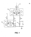
- FIG. 1 is a schematic diagram illustrating a circuit according to one embodiment of the present invention
- FIG. 2 is a graph associated with the circuit of FIG. 1;
- FIG. 3 is a schematic diagram illustrating a circuit according to one embodiment of the present invention.
- FIG. 4 is a graph associated with the circuit of FIG. 3.
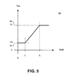
- FIG. 5 is a graph associated with the circuit of FIG. 3.
- a circuit in one aspect of the present invention, includes a current divider and a current mirror.
- the current divider may divide a current from a current source into a first and a second or reference current.
- the current mirror may be coupled to receive the first current from the current divider and an adjustment current, in an example.
- the adjustment current may set the reference current in the circuit and a resistor may be coupled to receive the reference current from the current divider to provide a reference voltage, in the example.
- the reference current and a reference voltage may be adjustable between two values, such as, for example, a full value of the reference current or voltage and a fraction of the full value of the reference current or voltage.
- FIG. 1 Shown schematically in FIG. 1 is a circuit 100 including a current divider 155 coupled to a current mirror 160, according to an example.
- current divider 155 may include a first transistor 110 including a first, second and third terminal 111, 112 and 113, respectively, and a second transistor 115 including a first, second and third terminal 116, 117 and 118, respectively.
- a first terminal 111 of first transistor 110 may be coupled to a first terminal 116 of second transistor 115.
- a current source 105 may be coupled to first transistor 110 and second transistor 115.
- a third transistor 135 including a first, second and third terminal 136, 137 and 138, respectively, and a fourth transistor 140 including a first, second and third terminal 141, 142 and 143, respectively, are included in current mirror 160.
- second terminal 112 of first transistor 110 may be coupled to first terminal 141 of fourth transistor 140, thus coupling current mirror 160 to current divider 155.
- transistors 110, 115, 135 and 140 of circuit 100 may include a metal oxide semiconductor field effect transistor (MOSFET).
- third transistor 135 and fourth transistor 140 may have respective strengths of the ratio 1:M, in the example.
- current divider 155 may divide a source current or current I 0 from a current source 105 into a first current Ix to be output from first transistor 110 and a second current or reference current I REF to be output from second transistor 115.
- first and second transistors 110 and 115 may have respective strengths related by a ratio of (1-r):r, where r is less than 1. Accordingly, in the example, a sum of first current Ix and reference current I REF may be substantially equal to a full value of the source current from current source 105 or current I 0 .
- current mirror 160 may be coupled to current divider 155 to receive first current Ix at first terminal 141 of third transistor 140.
- current mirror 160 may also be coupled to receive an adjustment current I A at second terminal 137 of third transistor 135.
- adjustment current I A may be mirrored to first current Ix.
- reference current I REF may be adjusted in response to adjustment current I A .
- adjustment current I A may set reference current I REF to an adjusted value between a full value of reference current I REF and a fraction, r, of the full value of the reference current I REF .
- a resistor 145 may be coupled to second terminal 117 of second transistor 115 to receive reference current I REF from current divider 155 to provide a reference voltage V REF .
- adjustment current I A may originate either inside or outside an integrated circuit that may contain circuit 100.
- the integrated circuit may control a power supply.
- FIG. 2 is a graph 200 depicting the relationship between adjustment current I A , indicated on a horizontal axis 201, and reference current I REF , indicated on vertical axis 203.
- a change in adjustment current I A and reference current I REF may be substantially linear or proportional when adjustment current I A is between an upper and a lower threshold value.
- reference current I REF is substantially equal to current I 0 , which is a full value 205 of reference current I REF . Because the sum of first current Ix and reference current I REF substantially equals current I 0 , when reference current I REF is at full value 205, first current Ix is equal to 0 (not shown), in the example.
- first current I x is the lesser of either mirrored adjustment current MI A or current (1-r)I 0 , in the example. Accordingly, in the example, because first current Ix may not exceed (1-r)I 0 , adjustment current I A may not reduce reference current I REF to less than a fractional value rI 0 . Thus, as shown in graph 200, as adjustment current I A increases, reference current I REF may decrease proportionally until it reaches fractional value rI 0 at 207 and first current Ix is equal to current (1-r)I 0 . In the example, adjustment current I A is then greater than or equal to the upper threshold value, (1-r)I 0 /M, in the example of FIG. 2. Note also, in the example, resistor 145 may receive reference current I REF to produce a reference voltage V REF .
- FIG. 3 illustrates an example circuit 300 associated with an implementation of circuit 100 (FIG. 1), in an example.
- circuit 300 may adjust a reference voltage V REF between a full value V 0 to a fraction of a full value rV 0 as a function of time.
- Circuit 300 may include a comparator 315 coupled to compare a sensed voltage V SENSE to reference voltage V REF to set an output 325 to a logic high value when a sensed voltage V SENSE exceeds reference voltage V REF , in accordance with an example.
- Circuit 300 may also include an input current source 310 coupled to first and second terminal 136 and 137 of third transistor 135 and coupled to receive an input current I RAMP , in the example.
- input current source 310 may remove a first threshold current I Z from input current I RAMP to produce adjustment current I A .
- FIG. 4 is a graph 400 of input current I RAMP as a function of time, during operation of circuit 300 of FIG. 3, in an example.
- input current I RAMP may decrease linearly with time from a value 402 that is greater than (1-r)I o plus a first threshold current Iz, for times less than t 1 , to a value that is less than first threshold current Iz, at 404 for times greater than t 2 .
- input current source 310 of FIG. 3 may reduce input current I RAMP by first threshold current Iz to produce adjustment current I A .
- first threshold current Iz may have a small value such as for example, approximately one microampere, to offset leakage current in I RAMP .
- first threshold current Iz may help to ensure that adjustment current I A goes to a value of zero.
- FIG. 5 further illustrates the adjustability of reference voltage V REF between two values, in an example.
- Graph 500 shows reference voltage V REF of circuit 300 (FIG. 3) as a function of time, in an example.
- Reference voltage V REF may be generated from reference current I REF and may therefore have a fractional value rV 0 at 501 for times less than t 1 , rise substantially linearly from rV 0 to a full value V 0 at 503, between time t 1 and t 2 , in the example. In the example, reference voltage V REF may then remain substantially at full value Vo for times greater than t 2 .
- parameters in the example circuits of FIGS. 1 and 3 may be controlled by design of circuits 100 and 300.
- the values of current I 0 of current source 105, first threshold current Iz and fractional value r may determine a first and a second value of reference voltage V REF or a full value and a fraction of a full value of reference voltage V REF .
- such values may be set with geometric ratios or by trimming on an integrated circuit.
Landscapes
- Engineering & Computer Science (AREA)
- Microelectronics & Electronic Packaging (AREA)
- Physics & Mathematics (AREA)
- Nonlinear Science (AREA)
- Electromagnetism (AREA)
- General Physics & Mathematics (AREA)
- Radar, Positioning & Navigation (AREA)
- Automation & Control Theory (AREA)
- Control Of Electrical Variables (AREA)
Abstract
Description
- The present invention relates generally to electrical circuits and, more specifically, the present invention relates to adjusting a reference in an electrical circuit.
- Integrated circuit controllers for switching power supplies use references such as reference voltages and reference currents to detect when internal and external parameters reach particular values. For example, a signal that senses a current in a switch is sometimes compared to a reference in order for a controller to switch off a power switch when the current exceeds a maximum value. Or, a signal proportional to a duty ratio may be compared to a reference so the controller can prevent the duty ratio from exceeding a maximum value. In another example, a signal proportional to an input voltage is compared to a reference to disable operation of a circuit when the input voltage is too high or too low.
- Oftentimes, a reference current or reference voltage needs to be adjusted for a particular application or a transient operating condition. In many cases, the reference needs to be changed in response to an external component or a dynamic stimulus. In addition, it is often desirable to adjust the reference between two values. Known techniques, however, for providing an integrated circuit solution can be costly.
- The present invention will be described by way of exemplary embodiments, but not limitations, illustrated in the accompanying drawings in which like references denote similar elements, and in which:
- FIG. 1 is a schematic diagram illustrating a circuit according to one embodiment of the present invention;
- FIG. 2 is a graph associated with the circuit of FIG. 1;
- FIG. 3 is a schematic diagram illustrating a circuit according to one embodiment of the present invention;
- FIG. 4 is a graph associated with the circuit of FIG. 3; and
- FIG. 5 is a graph associated with the circuit of FIG. 3.
- Examples of a circuit and method for adjusting a reference such as a reference current or a reference voltage are disclosed herein. In the following description, numerous specific details are set forth in order to provide a thorough understanding of the present invention. It will be apparent, however, to one having ordinary skill in the art that the specific detail need not be employed to practice the present invention. In other instances, well-known materials or methods have not been described in detail in order to avoid obscuring the present invention.
- Reference throughout this specification to "one embodiment" or "an embodiment" means that a particular feature, structure or characteristic described in connection with the embodiment is included in at least one embodiment of the present invention. Thus, the appearances of the phrases "in one embodiment" or "in an embodiment" in various places throughout this specification are not necessarily all referring to the same embodiment. Furthermore, the particular features, structures or characteristics may be combined in any suitable manner in one or more embodiments.
- In one aspect of the present invention, a circuit includes a current divider and a current mirror. In one example, the current divider may divide a current from a current source into a first and a second or reference current. The current mirror may be coupled to receive the first current from the current divider and an adjustment current, in an example. The adjustment current may set the reference current in the circuit and a resistor may be coupled to receive the reference current from the current divider to provide a reference voltage, in the example. Furthermore, in the example, the reference current and a reference voltage may be adjustable between two values, such as, for example, a full value of the reference current or voltage and a fraction of the full value of the reference current or voltage.
- Shown schematically in FIG. 1 is a
circuit 100 including acurrent divider 155 coupled to acurrent mirror 160, according to an example. As shown,current divider 155 may include afirst transistor 110 including a first, second andthird terminal second transistor 115 including a first, second andthird terminal first terminal 111 offirst transistor 110 may be coupled to afirst terminal 116 ofsecond transistor 115. In the example acurrent source 105 may be coupled tofirst transistor 110 andsecond transistor 115. - In addition, in the example, a
third transistor 135 including a first, second andthird terminal fourth transistor 140 including a first, second andthird terminal current mirror 160. As illustrated in the example,second terminal 112 offirst transistor 110 may be coupled tofirst terminal 141 offourth transistor 140, thus couplingcurrent mirror 160 tocurrent divider 155. Note that in the example,transistors circuit 100 may include a metal oxide semiconductor field effect transistor (MOSFET). In addition,third transistor 135 andfourth transistor 140 may have respective strengths of the ratio 1:M, in the example. - In operation,
current divider 155 may divide a source current or current I0 from acurrent source 105 into a first current Ix to be output fromfirst transistor 110 and a second current or reference current IREF to be output fromsecond transistor 115. In the example, first andsecond transistors current source 105 or current I0. - In the example,
current mirror 160 may be coupled tocurrent divider 155 to receive first current Ix atfirst terminal 141 ofthird transistor 140. In the example,current mirror 160 may also be coupled to receive an adjustment current IA atsecond terminal 137 ofthird transistor 135. Thus, in an example, adjustment current IA may be mirrored to first current Ix. Accordingly, in the example, reference current IREF may be adjusted in response to adjustment current IA. In particular, adjustment current IA may set reference current IREF to an adjusted value between a full value of reference current IREF and a fraction, r, of the full value of the reference current IREF. Furthermore, in the example, aresistor 145 may be coupled tosecond terminal 117 ofsecond transistor 115 to receive reference current IREF fromcurrent divider 155 to provide a reference voltage VREF. Note that in various examples, adjustment current IA may originate either inside or outside an integrated circuit that may containcircuit 100. In one example, the integrated circuit may control a power supply. - FIG. 2 is a
graph 200 depicting the relationship between adjustment current IA, indicated on ahorizontal axis 201, and reference current IREF, indicated onvertical axis 203. As illustrated in FIG. 2, a change in adjustment current IA and reference current IREF may be substantially linear or proportional when adjustment current IA is between an upper and a lower threshold value. Accordingly, in the example, when adjustment current IA is less than or equal to a lower threshold value such as 0, as in the example of FIG. 2, reference current IREF is substantially equal to current I0, which is afull value 205 of reference current IREF. Because the sum of first current Ix and reference current IREF substantially equals current I0, when reference current IREF is atfull value 205, first current Ix is equal to 0 (not shown), in the example. - Note that first current Ix is the lesser of either mirrored adjustment current MIA or current (1-r)I0, in the example. Accordingly, in the example, because first current Ix may not exceed (1-r)I0, adjustment current IA may not reduce reference current IREF to less than a fractional value rI0. Thus, as shown in
graph 200, as adjustment current IA increases, reference current IREF may decrease proportionally until it reaches fractional value rI0 at 207 and first current Ix is equal to current (1-r)I0. In the example, adjustment current IA is then greater than or equal to the upper threshold value, (1-r)I0/M, in the example of FIG. 2. Note also, in the example,resistor 145 may receive reference current IREF to produce a reference voltage VREF. - FIG. 3 illustrates an
example circuit 300 associated with an implementation of circuit 100 (FIG. 1), in an example. In the example,circuit 300 may adjust a reference voltage VREF between a full value V0 to a fraction of a full value rV0 as a function of time.Circuit 300 may include acomparator 315 coupled to compare a sensed voltage VSENSE to reference voltage VREF to set anoutput 325 to a logic high value when a sensed voltage VSENSE exceeds reference voltage VREF, in accordance with an example.Circuit 300 may also include aninput current source 310 coupled to first andsecond terminal third transistor 135 and coupled to receive an input current IRAMP, in the example. In the example, inputcurrent source 310 may remove a first threshold current IZ from input current IRAMP to produce adjustment current IA. - FIG. 4 is a
graph 400 of input current IRAMP as a function of time, during operation ofcircuit 300 of FIG. 3, in an example. As shown, in the example, input current IRAMP may decrease linearly with time from avalue 402 that is greater than (1-r)Io plus a first threshold current Iz, for times less than t1, to a value that is less than first threshold current Iz, at 404 for times greater than t2. In the example, inputcurrent source 310 of FIG. 3 may reduce input current IRAMP by first threshold current Iz to produce adjustment current IA. In the example of FIG. 3, the strengths oftransistors current mirror 160 of FIG. 1. In various examples, first threshold current Iz may have a small value such as for example, approximately one microampere, to offset leakage current in IRAMP. As a result, the presence of first threshold current Iz may help to ensure that adjustment current IA goes to a value of zero. - FIG. 5 further illustrates the adjustability of reference voltage VREF between two values, in an example. Graph 500 shows reference voltage VREF of circuit 300 (FIG. 3) as a function of time, in an example. Reference voltage VREF may be generated from reference current IREF and may therefore have a fractional value rV0 at 501 for times less than t1, rise substantially linearly from rV0 to a full value V0 at 503, between time t1 and t2, in the example. In the example, reference voltage VREF may then remain substantially at full value Vo for times greater than t2.
- In an example, parameters in the example circuits of FIGS. 1 and 3 may be controlled by design of
circuits current source 105, first threshold current Iz and fractional value r may determine a first and a second value of reference voltage VREF or a full value and a fraction of a full value of reference voltage VREF. In various examples, such values may be set with geometric ratios or by trimming on an integrated circuit. - In the foregoing detailed description, the method and apparatus of the present invention has been described with reference to specific exemplary embodiments thereof. It will, however, be evident that various modifications and changes may be made thereto without departing from the broader spirit and scope of the present invention. The present specification and figures are accordingly to be regarded as illustrative rather than restrictive.
Claims (20)
- A circuit, comprising:a current divider to divide a current from a current source into a first current and a reference current; anda current mirror coupled to the current divider to receive the first current from the current divider and to receive an adjustment current, the adjustment current to set the reference current.
- A circuit according to claim 1, further comprising a resistor coupled to receive the reference current from the current divider to provide a reference voltage.
- A circuit according to claim 1 or claim 2, wherein the current divider includes a first transistor and a second transistor, wherein a first terminal of the first transistor is coupled to a first terminal of the second transistor.
- A circuit according to claim 3, wherein the first and the second transistor have respective strengths related by a ratio of (1-r):r, wherein r is less than one.
- A circuit according to any preceding claim, wherein the reference current is adjustable between a full value and a fraction of the full value in response to the adjustment current.
- A circuit according to claim 5, wherein a change in the reference current and a change in the adjustment current are proportional when the adjustment current is between an upper and a lower threshold value.
- A circuit according to claim 6, wherein the first current is the current from the current source multiplied by (1-r) when the adjustment current is greater than the upper threshold value.
- A circuit according to claim 6, wherein the value of the first current is zero when a value of the adjustment current is less than the lower threshold value.
- A circuit according to any of claims 1 to 6, wherein the current from the current source is the sum of the first current and the reference current.
- A circuit according to any preceding claim, wherein the current mirror includes a third transistor and a fourth transistor with respective strengths of the ratio 1:M.
- A circuit according to claim 10, where the third and the fourth transistors include metal oxide semiconductor field effect transistors (MOSFETs).
- A circuit according to claim 10 or claim 11, wherein the third transistor is coupled to receive the adjustment current.
- A circuit according to claim 3, wherein the transistors in the current divider include metal oxide semiconductor field effect transistors (MOSFETs).
- A circuit according to any preceding claim, wherein the circuit is included in an integrated circuit.
- A circuit according to claim 14, wherein the integrated circuit is coupled to control a power supply.
- A method, comprising:dividing a source current into a first current and a second current such that a sum of the first and the second current is substantially equal to the source current;mirroring an adjustment current into the first current; andadjusting the second current in response to the adjustment current.
- A method according to claim 16, wherein adjusting the second current includes adjusting a reference current between a full value and a fraction of a full reference current value.
- A method according to claim 17, further comprising generating a reference voltage from the reference current.
- A method according to any of claims 16 to 18, further comprising receiving the source current from a current source.
- A method according to any of claims 16 to 19, further comprising reducing an input current by a first threshold current to produce the adjustment current.
Applications Claiming Priority (1)
| Application Number | Priority Date | Filing Date | Title |
|---|---|---|---|
| US11/493,504 US7397231B2 (en) | 2006-07-25 | 2006-07-25 | Method and apparatus for adjusting a reference |
Publications (1)
| Publication Number | Publication Date |
|---|---|
| EP1882998A1 true EP1882998A1 (en) | 2008-01-30 |
Family
ID=38520834
Family Applications (1)
| Application Number | Title | Priority Date | Filing Date |
|---|---|---|---|
| EP07252901A Withdrawn EP1882998A1 (en) | 2006-07-25 | 2007-07-23 | Method and apparatus for adjusting a reference |
Country Status (4)
| Country | Link |
|---|---|
| US (2) | US7397231B2 (en) |
| EP (1) | EP1882998A1 (en) |
| JP (1) | JP2008033934A (en) |
| CN (1) | CN101114178A (en) |
Families Citing this family (10)
| Publication number | Priority date | Publication date | Assignee | Title |
|---|---|---|---|---|
| US7397231B2 (en) * | 2006-07-25 | 2008-07-08 | Power Integrations, Inc. | Method and apparatus for adjusting a reference |
| US7502236B2 (en) | 2006-10-04 | 2009-03-10 | Power Integrations, Inc. | Power supply controller responsive to a feedforward signal |
| US7518885B2 (en) * | 2006-10-04 | 2009-04-14 | Power Integrations, Inc. | Method and apparatus for a control circuit with multiple operation modes |
| US7576528B2 (en) | 2006-10-04 | 2009-08-18 | Power Integrations, Inc. | Control circuit responsive to an impedance |
| ITTO20120479A1 (en) * | 2012-05-31 | 2013-12-01 | St Microelectronics Srl | GENERATION CIRCUIT OF AN ELECTRICITY OF CONFIGURABLE VALUE |
| CN103076834A (en) * | 2012-12-28 | 2013-05-01 | 四川和芯微电子股份有限公司 | Resistor calibrating circuit |
| KR102509586B1 (en) | 2016-08-17 | 2023-03-14 | 매그나칩 반도체 유한회사 | A generation circuit for bias current of reading otp cell and a control method thereof |
| US10819331B1 (en) * | 2019-05-07 | 2020-10-27 | Nxp B.V. | Self-regulating body-biasing techniques for process, voltage, and temperature (PVT) fluctuation compensation in fully-depleted silicon-on-insulator (FDSOI) semiconductors |
| WO2023277922A1 (en) | 2021-07-02 | 2023-01-05 | Power Integrations, Inc. | Adaptive ramp time modulation |
| US11996795B2 (en) | 2022-03-28 | 2024-05-28 | Power Integrations, Inc. | Motor alignment control |
Citations (1)
| Publication number | Priority date | Publication date | Assignee | Title |
|---|---|---|---|---|
| DE4119917A1 (en) * | 1990-06-18 | 1992-01-23 | Toyoda Automatic Loom Works | OVERCURRENT DETECTOR DEVICE |
Family Cites Families (4)
| Publication number | Priority date | Publication date | Assignee | Title |
|---|---|---|---|---|
| JPH08328676A (en) * | 1995-05-31 | 1996-12-13 | Nippon Motorola Ltd | Voltage source device for low voltage operation |
| KR100322527B1 (en) * | 1999-01-29 | 2002-03-18 | 윤종용 | Bandgap voltage reference circuit |
| DE10332864B4 (en) * | 2003-07-18 | 2007-04-26 | Infineon Technologies Ag | Voltage regulator with current mirror for decoupling a partial current |
| US7397231B2 (en) * | 2006-07-25 | 2008-07-08 | Power Integrations, Inc. | Method and apparatus for adjusting a reference |
-
2006
- 2006-07-25 US US11/493,504 patent/US7397231B2/en not_active Expired - Fee Related
-
2007
- 2007-07-23 EP EP07252901A patent/EP1882998A1/en not_active Withdrawn
- 2007-07-25 JP JP2007193174A patent/JP2008033934A/en not_active Withdrawn
- 2007-07-25 CN CNA2007101367183A patent/CN101114178A/en active Pending
-
2008
- 2008-06-06 US US12/135,087 patent/US7554315B2/en not_active Expired - Fee Related
Patent Citations (1)
| Publication number | Priority date | Publication date | Assignee | Title |
|---|---|---|---|---|
| DE4119917A1 (en) * | 1990-06-18 | 1992-01-23 | Toyoda Automatic Loom Works | OVERCURRENT DETECTOR DEVICE |
Also Published As
| Publication number | Publication date |
|---|---|
| JP2008033934A (en) | 2008-02-14 |
| US20080238401A1 (en) | 2008-10-02 |
| CN101114178A (en) | 2008-01-30 |
| US7554315B2 (en) | 2009-06-30 |
| US7397231B2 (en) | 2008-07-08 |
| US20080024105A1 (en) | 2008-01-31 |
Similar Documents
| Publication | Publication Date | Title |
|---|---|---|
| US7554315B2 (en) | Method and apparatus for adjusting a reference | |
| US9293990B2 (en) | Switching regulator and electronic apparatus | |
| KR101653001B1 (en) | Voltage regulator | |
| US8575906B2 (en) | Constant voltage regulator | |
| US11211864B2 (en) | Power supply device | |
| US10797689B2 (en) | Over-voltage clamp circuit | |
| US20090261797A1 (en) | Switching regulator | |
| US20030095368A1 (en) | Inrush current control method using a dual current limit power switch | |
| EP1708069A1 (en) | Overcurrent detecting circuit and regulator having the same | |
| JP2012088987A (en) | Semiconductor integrated circuit for regulators | |
| US9063558B2 (en) | Current limiting circuit configured to limit output current of driver circuit | |
| US20200395843A1 (en) | Integrated circuit and power supply circuit | |
| US20180196453A1 (en) | Voltage sensing mechanism to minimize short-to-ground current for low drop-out and bypass mode regulators | |
| US10756687B2 (en) | Switching controllers and methods for loads | |
| US10790752B1 (en) | Power supply device | |
| US11165337B2 (en) | Integrated circuit for power factor correction and power supply circuit containing the same | |
| EP3159994B1 (en) | Bidirectional current limiter | |
| US20160187900A1 (en) | Voltage regulator circuit and method for limiting inrush current | |
| US11057032B2 (en) | Control circuit and ideal diode circuit | |
| US7457138B2 (en) | Single pin multi-function signal detection method and structure therefor | |
| KR101319827B1 (en) | Current limit apparatus | |
| WO2019144962A1 (en) | Frequency control circuits for use in power factor correction circuits | |
| JP2006217695A (en) | Switching power supply | |
| JP2009211210A (en) | Power supply circuit device and electronic device | |
| US20240333136A1 (en) | Current limiting circuit |
Legal Events
| Date | Code | Title | Description |
|---|---|---|---|
| PUAI | Public reference made under article 153(3) epc to a published international application that has entered the european phase |
Free format text: ORIGINAL CODE: 0009012 |
|
| AK | Designated contracting states |
Kind code of ref document: A1 Designated state(s): AT BE BG CH CY CZ DE DK EE ES FI FR GB GR HU IE IS IT LI LT LU LV MC MT NL PL PT RO SE SI SK TR |
|
| AX | Request for extension of the european patent |
Extension state: AL BA HR MK YU |
|
| 17P | Request for examination filed |
Effective date: 20080221 |
|
| 17Q | First examination report despatched |
Effective date: 20080326 |
|
| RAP3 | Party data changed (applicant data changed or rights of an application transferred) |
Owner name: POWER INTEGRATIONS, INC. |
|
| AKX | Designation fees paid |
Designated state(s): DE FR GB IT NL SE |
|
| STAA | Information on the status of an ep patent application or granted ep patent |
Free format text: STATUS: THE APPLICATION IS DEEMED TO BE WITHDRAWN |
|
| 18D | Application deemed to be withdrawn |
Effective date: 20100615 |