EP1881597A1 - Multilevel LINC transmitter - Google Patents
Multilevel LINC transmitter Download PDFInfo
- Publication number
- EP1881597A1 EP1881597A1 EP07110010A EP07110010A EP1881597A1 EP 1881597 A1 EP1881597 A1 EP 1881597A1 EP 07110010 A EP07110010 A EP 07110010A EP 07110010 A EP07110010 A EP 07110010A EP 1881597 A1 EP1881597 A1 EP 1881597A1
- Authority
- EP
- European Patent Office
- Prior art keywords
- multilevel
- coupled
- linc transmitter
- scaler
- block
- Prior art date
- Legal status (The legal status is an assumption and is not a legal conclusion. Google has not performed a legal analysis and makes no representation as to the accuracy of the status listed.)
- Granted
Links
Images





Classifications
-
- H—ELECTRICITY
- H03—ELECTRONIC CIRCUITRY
- H03F—AMPLIFIERS
- H03F1/00—Details of amplifiers with only discharge tubes, only semiconductor devices or only unspecified devices as amplifying elements
- H03F1/02—Modifications of amplifiers to raise the efficiency, e.g. gliding Class A stages, use of an auxiliary oscillation
- H03F1/0205—Modifications of amplifiers to raise the efficiency, e.g. gliding Class A stages, use of an auxiliary oscillation in transistor amplifiers
- H03F1/0294—Modifications of amplifiers to raise the efficiency, e.g. gliding Class A stages, use of an auxiliary oscillation in transistor amplifiers using vector summing of two or more constant amplitude phase-modulated signals
-
- H—ELECTRICITY
- H03—ELECTRONIC CIRCUITRY
- H03F—AMPLIFIERS
- H03F1/00—Details of amplifiers with only discharge tubes, only semiconductor devices or only unspecified devices as amplifying elements
- H03F1/02—Modifications of amplifiers to raise the efficiency, e.g. gliding Class A stages, use of an auxiliary oscillation
- H03F1/0205—Modifications of amplifiers to raise the efficiency, e.g. gliding Class A stages, use of an auxiliary oscillation in transistor amplifiers
-
- H—ELECTRICITY
- H03—ELECTRONIC CIRCUITRY
- H03F—AMPLIFIERS
- H03F1/00—Details of amplifiers with only discharge tubes, only semiconductor devices or only unspecified devices as amplifying elements
- H03F1/02—Modifications of amplifiers to raise the efficiency, e.g. gliding Class A stages, use of an auxiliary oscillation
- H03F1/0205—Modifications of amplifiers to raise the efficiency, e.g. gliding Class A stages, use of an auxiliary oscillation in transistor amplifiers
- H03F1/0211—Modifications of amplifiers to raise the efficiency, e.g. gliding Class A stages, use of an auxiliary oscillation in transistor amplifiers with control of the supply voltage or current
- H03F1/0244—Stepped control
- H03F1/025—Stepped control by using a signal derived from the input signal
-
- H—ELECTRICITY
- H03—ELECTRONIC CIRCUITRY
- H03F—AMPLIFIERS
- H03F3/00—Amplifiers with only discharge tubes or only semiconductor devices as amplifying elements
- H03F3/20—Power amplifiers, e.g. Class B amplifiers, Class C amplifiers
- H03F3/24—Power amplifiers, e.g. Class B amplifiers, Class C amplifiers of transmitter output stages
-
- H—ELECTRICITY
- H03—ELECTRONIC CIRCUITRY
- H03F—AMPLIFIERS
- H03F2200/00—Indexing scheme relating to amplifiers
- H03F2200/468—Indexing scheme relating to amplifiers the temperature being sensed
Definitions
- the invention relates to a LINC transmitter (a transmitter having a LINC architecture) and, in particular, to a multilevel LINC transmitter.
- Linear amplification with nonlinear components is a transmitter architecture which increases linearity and power efficiency of a wireless transmitter. Due to accurate signal processing and insensitivity to process variation, a digital LINC architecture is more suitable for modem process technologies.
- Fig. 1 is a block diagram of a conventional LINC architecture.
- an input signal S(t) of the LINC 100 is a varying envelope signal.
- a signal separator 110 receives and divides the input signal S(t) into two constant-envelope signals S1 and S2.
- two power amplifiers PA1 and PA2 respectively amplify the constant-envelope signals S1 and S2. Since a nonlinear power amplifier can amplify a constant-envelope signal linearly, two power efficient nonlinear power amplifiers are used in such architecture.
- the two amplified signals are combined by a power combiner 120.
- a linearly amplified signal is obtained at an output of the power combiner 120.
- S(t) denotes the signal envelope
- ⁇ (t) is signal phase.
- Both S 1 (t) and S 2 (t) are on a circle with a radius r 0 .
- r 0 is a constant scale factor predefined by a system designer. Because input range of an inverse cosine function is [-1, 1], selection of r 0 needs to satisfy the formula: r 0 ⁇ max A t
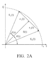
- Fig. 2B illustrates the signals after amplification.
- the amplified signals are expressed as G . S 1 (t) and G . S 2 (t), where G is voltage gain of the power amplifiers.
- the two amplified signals are combined by a power combiner to obtain a signal ⁇ 2G ⁇ S (t) which is a linear amplification of the input signal S(t). Because of the out-phasing technique, LINC achieves linear amplification with two power efficient nonlinear power amplifiers.
- An embodiment of a multilevel LINC transmitter comprises a multilevel signal component separator, a phase modulator block, and an RF block.
- the multilevel signal component separator comprises a multilevel scaler and converts an input signal to phase signals.
- the phase modulator block is coupled to the multilevel signal component separator.
- the RF block comprises a plurality of power amplifiers coupled to the phase modulator block and the multilevel scaler and a power combiner coupled to the power amplifiers.
- the invention provides a multilevel LINC transmitter with a multilevel scaler in a multilevel signal component separator thereof.
- the multilevel scaler dynamically adapts a scale factor according to the input signal and therefore the out-phasing angle is adjustable. As a result, high power efficiency and linearity are achieved.
- Fig. 1 is a block diagram of a conventional LINC architecture
- Figs. 2A and 2B are respectively phasor diagrams of a signal and components thereof before and after amplification
- Fig. 3 is a block diagram of a multilevel LINC transmitter according to an embodiment of the invention.
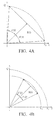
- Figs. 4A and 4B are respectively phasor diagrams showing out-phasing angles of single-level and multilevel scaling techniques
- Figs. 5A and 5B are respectively a detailed phasor diagram and a generalized phasor diagram showing out-phasing angles of multilevel scaling techniques
- Fig. 6 is a schematic diagram showing signal envelope distribution in WCDMA
- Fig. 7 is a block diagram of a multilevel scaler 313 in Fig. 3;
- Fig. 8 is a block diagram of the envelope modulator 340 in Fig. 3;
- Fig. 9A is a schematic diagram of VDD-to-PM distortion which degrades linearity
- Fig. 9B is a schematic diagram showing characteristics of the distortion compensator 350 in Fig. 3.
- Fig. 9C is a schematic diagram showing constant phase of the output signal of the multilevel LINC transmitter with different PA supply votlages.
- Fig. 3 is a block diagram of a multilevel LINC transmitter according to an embodiment of the invention.
- the multilevel LINC transmitter 300 comprises a multilevel signal component separator 310, a phase modulator block 320, and an RF block 330.
- the multilevel signal component separator 310 comprises a polar converter 311, a multilevel scaler 313 coupled to the polar converter 311, an inverse cosine module 315 coupled to the multilevel scaler 313, and a phase calculator 317 coupled to the polar converter 311 and the inverse cosine module 315.
- the polar converter 311 receives and converts the input signal S(t) to polar form.
- an envelope signal A(t) is scaled by a multilevel scaler 313 and the inverse cosine module 315 generates an out-phasing angle ⁇ '(t).
- the phase calculator 317 generates phase signals ⁇ (t)+ ⁇ '(t) and ⁇ (t)- ⁇ '(t).
- the multilevel signal component separator 310 converts the input signal S(t) into phase signals ⁇ (t)+ ⁇ '(t) and ( ⁇ (t)- ⁇ '(t).
- the phase modulator block 320 comprises two phase modulators 321 coupled to the multilevel signal component separator 310.
- the RF block 330 comprises a plurality power amplifiers 331 coupled to the phase modulator block 320 and the multilevel scaler 313 and a power combiner 333 coupled to the power amplifiers 331.
- a Wilkinson power combiner is adopted in a LINC transmitter, however, scope of the invention is not limited thereto.
- Other hybrid couplers, lossless Wilkinson power combiner, Chireix-outphasing combiner, or the like are also applicable to the invention.
- the multilevel scaler 313 in Fig. 3 reduces ⁇ (t) such that high Wilkinson power combiner efficiency is achieved.
- a 2-level design example is illustrated in Fig. 4B.
- the multilevel scaler adapts scale factor from r 0 to r 1 ., and out-phasing angle.
- ⁇ '(t) in Fig. 4B is much smaller than the conventional out-phasing angle ⁇ (t) in Fig. 4A.
- the multilevel scaling technique can be generalized to N levels in Fig.
- Fig. 6 shows envelope distribution of WCDMA where A(t) is a probability function. To acquire an expected value of ⁇ (t), the envelope A(t) is divided into several regions, illustrated in Fig. 5.
- an optimal set of R N is obtained.
- the multilevel scaler dynamically adapts R N close to and no lower than the envelope A(t).
- Fig. 7 is a block diagram of a multilevel scaler 313 in Fig. 3.
- the multilevel scaler 313 comprises a slicer 510 and a ROM 530 coupled to the slicer 510.
- the slicer 510 is used to select and output a specific r k to the inverse cosine module 315.
- the slicer 510 comprises a comparator.
- the comparator determines in which range the envelope A(t) is and which r k should be selected according thereto.
- the ROM 530 stores the optimal set of R N .
- the multilevel LINC transmitter further comprises an envelope modulator 340 coupled to the multilevel scaler 313 and the power amplifiers 331, as shown in Fig. 3.
- Fig. 8 is a block diagram of the envelope modulator 340 in Fig. 3.
- the envelope modulator 340 comprises a digital to analog converter (DAC) 341 coupled to the multilevel scaler 313, a low pass filter (LPF) 343 coupled between the DAC 341, and a low low drop-out (LDO) regulator 345 coupled between the LPF 343 and the power amplifier 331.
- An input signal of the envelope modulator 340 is a digital control signal from the multilevel scaler 313.
- the digital-to-analog converter (DAC) 341 converts the control signal to an analog signal.
- the analog control signal passes through the low pass filter (LPF) 343.
- the highly power efficient low drop out (LDO) regulator 345 ensures a robust power supply voltage to the PA 331. Due to RC delay, the control signal path group delay and the phase path delay are different. An additional delay compensator is inserted in a phase path, between the phase modulator block and the RF block, to partially overcome distortion due to RC delay.
- the multilevel LINC transmitter further comprises a distortion compensator 350 coupled between the multilevel signal component separator 310 and the envelope modulator 340. Since adjustment of the supply voltage of two RF power amplifiers 331 introduces another distortion, VDD-to-PM distortion, a distortion compensator 350 is incorporated in the multilevel LINC transmitter to compensate VDD-to-PM distortion.
- Fig. 9A is a schematic diagram of VDD-to-PM distortion which degrades linearity.
- a digital distortion compensator 350 with characteristics shown in Fig. 9B is incorporated in the multilevel LINC transmitter.
- phase of the output signal remains constant even with different PA supply voltages, as shown in Fig. 9C.
- the multilevel LINC transmitter according to an embodiment of the invention further comprises a temperature sensor 360. Since temperature variation may result in different VDD-to-PM distortion, a temperature sensor 360 is incorporated in the the multilevel LINC transmitter such that VDD-to-PM distortion is compensated.
- the invention provides a multilevel LINC transmitter with a multilevel scaler in a multilevel signal component separator thereof.
- the multilevel scaler dynamically adapts a scale factor according to the input signal and therefore the out-phasing angle is adjustable.. As a result, high power efficiency and linearity are achieved.
Landscapes
- Engineering & Computer Science (AREA)
- Power Engineering (AREA)
- Amplifiers (AREA)
- Transmitters (AREA)
Abstract
Description
- This application claims the benefit of
U.S. Provisional Application No. 60/807,952, filed on July 21, 2006 U.S. Application No. 11/757,479, filed on June 4, 2007 - The invention relates to a LINC transmitter (a transmitter having a LINC architecture) and, in particular, to a multilevel LINC transmitter.
- To prolong battery life of mobile handset devices, demands on power efficiency of wireless mobile communication systems have become more important. In general, the most power hungry device in a transceiver is a power amplifier which has nonlinear characteristics. In addition, modulation of non-constant-envelope signals demands high linearity of a power amplifier. As a result, a trade off between linearity and power efficiency in a wireless transmitter is necessary.
- Various PA linearization techniques have been adopted to improve linearity and power efficiency of wireless transmitters. Linear amplification with nonlinear components (LINC) is a transmitter architecture which increases linearity and power efficiency of a wireless transmitter. Due to accurate signal processing and insensitivity to process variation, a digital LINC architecture is more suitable for modem process technologies.
- Fig. 1 is a block diagram of a conventional LINC architecture. As shown in Fig. 1, an input signal S(t) of the
LINC 100 is a varying envelope signal. Asignal separator 110 receives and divides the input signal S(t) into two constant-envelope signals S1 and S2. Subsequently, two power amplifiers PA1 and PA2 respectively amplify the constant-envelope signals S1 and S2. Since a nonlinear power amplifier can amplify a constant-envelope signal linearly, two power efficient nonlinear power amplifiers are used in such architecture. Finally, the two amplified signals are combined by a power combiner 120. Thus, a linearly amplified signal is obtained at an output of the power combiner 120. - The input of the LINC system is a varying-envelope signal S(t),


- Fig. 2B illustrates the signals after amplification. The amplified signals are expressed as G . S1(t) and G . S2(t), where G is voltage gain of the power amplifiers. The two amplified signals are combined by a power combiner to obtain a signal √2G·S(t) which is a linear amplification of the input signal S(t). Because of the out-phasing technique, LINC achieves linear amplification with two power efficient nonlinear power amplifiers.
- An embodiment of a multilevel LINC transmitter comprises a multilevel signal component separator, a phase modulator block, and an RF block. The multilevel signal component separator comprises a multilevel scaler and converts an input signal to phase signals. The phase modulator block is coupled to the multilevel signal component separator. The RF block comprises a plurality of power amplifiers coupled to the phase modulator block and the multilevel scaler and a power combiner coupled to the power amplifiers.
- The invention provides a multilevel LINC transmitter with a multilevel scaler in a multilevel signal component separator thereof. The multilevel scaler dynamically adapts a scale factor according to the input signal and therefore the out-phasing angle is adjustable. As a result, high power efficiency and linearity are achieved.
- A detailed description is given in the following embodiments with reference to the accompanying drawings.
- The invention can be more fully understood by reading the subsequent detailed description and examples with references made to the accompanying drawings, wherein:
- Fig. 1 is a block diagram of a conventional LINC architecture;
- Figs. 2A and 2B are respectively phasor diagrams of a signal and components thereof before and after amplification;
- Fig. 3 is a block diagram of a multilevel LINC transmitter according to an embodiment of the invention;
- Figs. 4A and 4B are respectively phasor diagrams showing out-phasing angles of single-level and multilevel scaling techniques;
- Figs. 5A and 5B are respectively a detailed phasor diagram and a generalized phasor diagram showing out-phasing angles of multilevel scaling techniques;
- Fig. 6 is a schematic diagram showing signal envelope distribution in WCDMA;
- Fig. 7 is a block diagram of a
multilevel scaler 313 in Fig. 3; - Fig. 8 is a block diagram of the
envelope modulator 340 in Fig. 3; - Fig. 9A is a schematic diagram of VDD-to-PM distortion which degrades linearity;
- Fig. 9B is a schematic diagram showing characteristics of the
distortion compensator 350 in Fig. 3; and - Fig. 9C is a schematic diagram showing constant phase of the output signal of the multilevel LINC transmitter with different PA supply votlages.
- The following description is of the best-contemplated mode of carrying out the invention. This description is made for the purpose of illustrating the general principles of the invention and should not be taken in a limiting sense. The scope of the invention is best determined by reference to the appended claims.
- Fig. 3 is a block diagram of a multilevel LINC transmitter according to an embodiment of the invention. The multilevel LINC transmitter 300 comprises a multilevel
signal component separator 310, aphase modulator block 320, and anRF block 330. The multilevelsignal component separator 310 comprises apolar converter 311, amultilevel scaler 313 coupled to thepolar converter 311, aninverse cosine module 315 coupled to themultilevel scaler 313, and aphase calculator 317 coupled to thepolar converter 311 and theinverse cosine module 315. Thepolar converter 311 receives and converts the input signal S(t) to polar form. Then, an envelope signal A(t) is scaled by amultilevel scaler 313 and theinverse cosine module 315 generates an out-phasing angle θ'(t). Thereafter, thephase calculator 317 generates phase signals ϕ(t)+θ'(t) and ϕ(t)-θ'(t). In other words, the multilevelsignal component separator 310 converts the input signal S(t) into phase signals ϕ(t)+θ'(t) and (ϕ(t)-θ'(t). Thephase modulator block 320 comprises twophase modulators 321 coupled to the multilevelsignal component separator 310. TheRF block 330 comprises aplurality power amplifiers 331 coupled to thephase modulator block 320 and themultilevel scaler 313 and apower combiner 333 coupled to thepower amplifiers 331. - In an embodiment of the invention, a Wilkinson power combiner is adopted in a LINC transmitter, however, scope of the invention is not limited thereto. Other hybrid couplers, lossless Wilkinson power combiner, Chireix-outphasing combiner, or the like are also applicable to the invention. For a Wilkinson power combiner, efficiency η(t) thereof is defined as,


- Rather than the conventional scaling technique using single-level r0, the
multilevel scaler 313 in Fig. 3 reduces θ(t) such that high Wilkinson power combiner efficiency is achieved. A 2-level design example is illustrated in Fig. 4B. When A(t) is much smaller than r0, the multilevel scaler adapts scale factor from r0 to r1., and out-phasing angle. θ'(t) in Fig. 4B is much smaller than the conventional out-phasing angle θ(t) in Fig. 4A. Thus, the multilevel scaling technique enhances Wilkinson combiner efficiency. The multilevel scaling technique can be generalized to N levels in Fig. 5A, and RN is a general expression for multilevel scaling as shown in Fig. 5B, where RN = rk, for r k+1<A(t) ≤rk k = 0,1,..., N - 1, where rN = 0, r 0 = max(A(t)) . The definition of out-phasing angle θ'(t) in multilevel scaling technique is modified as
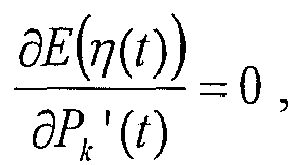
- To maximize the Wilkinson power combiner efficiency, optimal scale factors of each level rk need to be determined in advance. Since multilevel scale factors are used in the LINC transmitter, Wilkinson power combiner efficiency formula is modified as


- Fig. 7 is a block diagram of a
multilevel scaler 313 in Fig. 3. Themultilevel scaler 313 comprises aslicer 510 and aROM 530 coupled to theslicer 510. Theslicer 510 is used to select and output a specific rk to theinverse cosine module 315. Preferably, theslicer 510 comprises a comparator. The comparator determines in which range the envelope A(t) is and which rk should be selected according thereto. TheROM 530 stores the optimal set of RN. - Moreover, the multilevel LINC transmitter according to an embodiment of the invention further comprises an
envelope modulator 340 coupled to themultilevel scaler 313 and thepower amplifiers 331, as shown in Fig. 3. Fig. 8 is a block diagram of theenvelope modulator 340 in Fig. 3. Theenvelope modulator 340 comprises a digital to analog converter (DAC) 341 coupled to themultilevel scaler 313, a low pass filter (LPF) 343 coupled between theDAC 341, and a low low drop-out (LDO)regulator 345 coupled between theLPF 343 and thepower amplifier 331. An input signal of theenvelope modulator 340 is a digital control signal from themultilevel scaler 313. The digital-to-analog converter (DAC) 341 converts the control signal to an analog signal. Then the analog control signal passes through the low pass filter (LPF) 343. Finally, the highly power efficient low drop out (LDO)regulator 345 ensures a robust power supply voltage to thePA 331. Due to RC delay, the control signal path group delay and the phase path delay are different. An additional delay compensator is inserted in a phase path, between the phase modulator block and the RF block, to partially overcome distortion due to RC delay. - Additionally, the multilevel LINC transmitter according to an embodiment of the invention further comprises a
distortion compensator 350 coupled between the multilevelsignal component separator 310 and theenvelope modulator 340. Since adjustment of the supply voltage of twoRF power amplifiers 331 introduces another distortion, VDD-to-PM distortion, adistortion compensator 350 is incorporated in the multilevel LINC transmitter to compensate VDD-to-PM distortion. Fig. 9A is a schematic diagram of VDD-to-PM distortion which degrades linearity. To correct VDD-to-PM distortion, adigital distortion compensator 350 with characteristics shown in Fig. 9B is incorporated in the multilevel LINC transmitter. Thus, phase of the output signal remains constant even with different PA supply voltages, as shown in Fig. 9C. - Moreover, the multilevel LINC transmitter according to an embodiment of the invention further comprises a
temperature sensor 360. Since temperature variation may result in different VDD-to-PM distortion, atemperature sensor 360 is incorporated in the the multilevel LINC transmitter such that VDD-to-PM distortion is compensated. - The invention provides a multilevel LINC transmitter with a multilevel scaler in a multilevel signal component separator thereof. The multilevel scaler dynamically adapts a scale factor according to the input signal and therefore the out-phasing angle is adjustable.. As a result, high power efficiency and linearity are achieved.
- While the invention has been described by way of example and in terms of preferred embodiment, it is to be understood that the invention is not limited thereto. To the contrary, it is intended to cover various modifications and similar arrangements as would be apparent to those skilled in the art. Therefore, the scope of the appended claims should be accorded the broadest interpretation so as to encompass all such modifications and similar arrangements.
Claims (10)
- A multilevel LINC transmitter, comprising:a multilevel signal component separator (310) comprising a multilevel scaler (313) and converting an input signal to phase signals;a phase modulator block (320) coupled to the multilevel signal component separator (310); andan RF block (330) comprising a plurality of power amplifiers (331) coupled to the phase modulator block (320) and the multilevel scaler (313) and a power combiner (333) coupled to the power amplifiers.
- The multilevel LINC transmitter as claimed in claim 1, wherein the multilevel scaler (313) comprises an slicer (510) and a ROM (530) coupled to the slicer.
- The multilevel LINC transmitter as claimed in claim 2, wherein the slicer comprises a comparator.
- The multilevel LINC transmitter as claimed in any of the preceding claims, further comprising an envelope modulator (340) coupled to the multilevel scaler (313) and the power amplifiers (331).
- The multilevel LINC transmitter as claimed in claim 4, wherein the envelope modulator (340) comprises a digital to analog converter (341; DAC) coupled to the multilevel scaler (313) and a low pass filter (343; LPF) coupled between the DAC (341) and the power amplifiers (331).
- The multilevel LINC transmitter as claimed in claim 5, wherein the envelope modulator (340) further comprises a low drop-out (LDO) regulator (345) coupled between the LPF (343) and the power amplifier (331).
- The multilevel LINC transmitter as claimed in claim 6, further comprising a delay compensator coupled between the phase modulator block (320) and the RF block (330).
- The multilevel LINC transmitter as claimed in any of the preceding claims, further comprising a distortion compensator (350) coupled between the multilevel signal component separator (310) and the envelope modulator (340).
- The multilevel LINC transmitter as claimed in claim 8, further comprising a sensor (360) coupled to the distortion compensator (350).
- The multilevel LINC transmitter as claimed in any of the preceding claims, wherein the power combiner (333) is a Wilkinson combiner.
Applications Claiming Priority (2)
| Application Number | Priority Date | Filing Date | Title |
|---|---|---|---|
| US80795206P | 2006-07-21 | 2006-07-21 | |
| US11/757,479 US7724839B2 (en) | 2006-07-21 | 2007-06-04 | Multilevel LINC transmitter |
Publications (2)
| Publication Number | Publication Date |
|---|---|
| EP1881597A1 true EP1881597A1 (en) | 2008-01-23 |
| EP1881597B1 EP1881597B1 (en) | 2011-10-19 |
Family
ID=38559734
Family Applications (1)
| Application Number | Title | Priority Date | Filing Date |
|---|---|---|---|
| EP07110010A Active EP1881597B1 (en) | 2006-07-21 | 2007-06-11 | Multilevel LINC transmitter |
Country Status (3)
| Country | Link |
|---|---|
| US (1) | US7724839B2 (en) |
| EP (1) | EP1881597B1 (en) |
| TW (1) | TWI349445B (en) |
Cited By (7)
| Publication number | Priority date | Publication date | Assignee | Title |
|---|---|---|---|---|
| GB2463511A (en) * | 2008-09-10 | 2010-03-17 | Asahi Kasei Emd Corp | A class E amplifier with power supply modulation and a predistorted input signal |
| EP2388912A1 (en) * | 2010-05-04 | 2011-11-23 | Nxp B.V. | Power control of reconfigurable outphasing Chireix amplifiers and methods |
| US8203386B2 (en) | 2010-05-04 | 2012-06-19 | Nxp B.V. | Reconfigurable outphasing Chireix amplifiers and methods |
| EP2840710A1 (en) * | 2013-08-20 | 2015-02-25 | Analog Devices Technology | Power amplification system, device and method |
| KR20150022979A (en) * | 2012-06-18 | 2015-03-04 | 알더블유티에이치 아헨 | Amplifier assembly |
| WO2016206478A1 (en) * | 2015-06-26 | 2016-12-29 | 深圳市中兴微电子技术有限公司 | Link balancing method and device, and storage medium |
| EP3264706A3 (en) * | 2016-07-01 | 2018-04-18 | Intel IP Corporation | Low drop out compensation technique for reduced dynamic errors in digital-to-time converters |
Families Citing this family (59)
| Publication number | Priority date | Publication date | Assignee | Title |
|---|---|---|---|---|
| US7355470B2 (en) | 2006-04-24 | 2008-04-08 | Parkervision, Inc. | Systems and methods of RF power transmission, modulation, and amplification, including embodiments for amplifier class transitioning |
| US7327803B2 (en) | 2004-10-22 | 2008-02-05 | Parkervision, Inc. | Systems and methods for vector power amplification |
| US7911272B2 (en) | 2007-06-19 | 2011-03-22 | Parkervision, Inc. | Systems and methods of RF power transmission, modulation, and amplification, including blended control embodiments |
| US8334722B2 (en) | 2007-06-28 | 2012-12-18 | Parkervision, Inc. | Systems and methods of RF power transmission, modulation and amplification |
| US8013675B2 (en) | 2007-06-19 | 2011-09-06 | Parkervision, Inc. | Combiner-less multiple input single output (MISO) amplification with blended control |
| US8031804B2 (en) | 2006-04-24 | 2011-10-04 | Parkervision, Inc. | Systems and methods of RF tower transmission, modulation, and amplification, including embodiments for compensating for waveform distortion |
| US8315336B2 (en) | 2007-05-18 | 2012-11-20 | Parkervision, Inc. | Systems and methods of RF power transmission, modulation, and amplification, including a switching stage embodiment |
| KR20100059974A (en) * | 2007-09-27 | 2010-06-04 | 교세라 가부시키가이샤 | Power amplifying circuit, and transmitter and wireless communication device using the same |
| US7994854B2 (en) * | 2008-01-29 | 2011-08-09 | Nxp B.V. | Circuit with a power amplifier and amplification method |
| WO2009114731A2 (en) | 2008-03-13 | 2009-09-17 | Viasat, Inc. | Multi-level power amplification system |
| US8212541B2 (en) | 2008-05-08 | 2012-07-03 | Massachusetts Institute Of Technology | Power converter with capacitive energy transfer and fast dynamic response |
| WO2009145887A1 (en) * | 2008-05-27 | 2009-12-03 | Parkervision, Inc. | Systems and methods of rf power transmission, modulation, and amplification |
| TWI419464B (en) * | 2008-07-21 | 2013-12-11 | Applied Materials Inc | Apparatus for dual frequency power application |
| US8145157B2 (en) * | 2008-09-30 | 2012-03-27 | Infineon Technologies Ag | High efficiency modulation |
| EP2353219B1 (en) | 2008-11-11 | 2018-05-02 | Massachusetts Institute of Technology | An asymmetric multilevel outphasing architecture for rf amplifiers |
| US9634577B2 (en) | 2008-11-11 | 2017-04-25 | Massachusetts Institute Of Technology | Inverter/power amplifier with capacitive energy transfer and related techniques |
| US9912303B2 (en) * | 2010-02-03 | 2018-03-06 | Massachusetts Institute Of Technology | RF-input / RF-output outphasing amplifier |
| US10389235B2 (en) | 2011-05-05 | 2019-08-20 | Psemi Corporation | Power converter |
| KR20140026458A (en) | 2011-04-08 | 2014-03-05 | 파커비전, 인크. | Systems and methods of rf power transmission, modulation, and amplification |
| US10129055B2 (en) | 2011-04-21 | 2018-11-13 | Mediatek Singapore Pte. Ltd. | PA cell, PA module, wireless communication unit, RF transmitter architecture and method therefor |
| US9379742B2 (en) | 2011-04-21 | 2016-06-28 | Mediatek Singapore Pte. Ltd. | RF transmitter, integrated circuit device, wireless communication unit and method therefor |
| US9559879B2 (en) | 2011-04-21 | 2017-01-31 | Mediatek Singapore Pte. Ltd. | PA cell, PA module, wireless communication unit, RF transmitter architecture and method therefor |
| US9088319B2 (en) | 2011-04-21 | 2015-07-21 | Mediatek Singapore Pte. Ltd. | RF transmitter architecture, integrated circuit device, wireless communication unit and method therefor |
| US9647866B2 (en) | 2011-04-21 | 2017-05-09 | Mediatek Singapore Pte, Ltd. | RF transmitter, integrated circuit device, wireless communication unit and method therefor |
| US10680515B2 (en) | 2011-05-05 | 2020-06-09 | Psemi Corporation | Power converters with modular stages |
| CN108964442A (en) | 2011-05-05 | 2018-12-07 | 北极砂技术有限公司 | Device for power supply conversion |
| US9882471B2 (en) | 2011-05-05 | 2018-01-30 | Peregrine Semiconductor Corporation | DC-DC converter with modular stages |
| JP6174574B2 (en) | 2011-06-02 | 2017-08-02 | パーカーヴィジョン インコーポレイテッド | Antenna control |
| GB2488380B (en) | 2011-06-24 | 2018-04-04 | Snaptrack Inc | Envelope tracking system for mimo |
| JP5731326B2 (en) * | 2011-08-26 | 2015-06-10 | 富士通株式会社 | Modulator and amplifier using the same |
| US8743553B2 (en) | 2011-10-18 | 2014-06-03 | Arctic Sand Technologies, Inc. | Power converters with integrated capacitors |
| US8723491B2 (en) | 2011-12-19 | 2014-05-13 | Arctic Sand Technologies, Inc. | Control of power converters with capacitive energy transfer |
| US8964881B2 (en) | 2012-08-16 | 2015-02-24 | Massachusetts Institute Of Technology | Method and apparatus for high efficiency, high dynamic range digital RF power amplification |
| US9537456B2 (en) | 2012-10-30 | 2017-01-03 | Eta Devices, Inc. | Asymmetric multilevel backoff amplifier with radio-frequency splitter |
| US8824978B2 (en) | 2012-10-30 | 2014-09-02 | Eta Devices, Inc. | RF amplifier architecture and related techniques |
| US9166536B2 (en) | 2012-10-30 | 2015-10-20 | Eta Devices, Inc. | Transmitter architecture and related methods |
| US8829993B2 (en) | 2012-10-30 | 2014-09-09 | Eta Devices, Inc. | Linearization circuits and methods for multilevel power amplifier systems |
| US8724353B1 (en) | 2013-03-15 | 2014-05-13 | Arctic Sand Technologies, Inc. | Efficient gate drivers for switched capacitor converters |
| US8619445B1 (en) | 2013-03-15 | 2013-12-31 | Arctic Sand Technologies, Inc. | Protection of switched capacitor power converter |
| US9660520B2 (en) | 2013-04-09 | 2017-05-23 | Massachusetts Institute Of Technology | Method and apparatus to provide power conversion with high power factor |
| KR20150007404A (en) * | 2013-07-10 | 2015-01-21 | 한국전자통신연구원 | Apparatus and method for amplifier signal |
| EP3047348B1 (en) | 2013-09-17 | 2025-03-19 | Parkervision, Inc. | Method for rendering an information bearing function of time |
| US10840805B2 (en) | 2013-09-24 | 2020-11-17 | Eta Devices, Inc. | Integrated power supply and modulator for radio frequency power amplifiers |
| US9755672B2 (en) | 2013-09-24 | 2017-09-05 | Eta Devices, Inc. | Integrated power supply and modulator for radio frequency power amplifiers |
| WO2015069516A1 (en) | 2013-10-29 | 2015-05-14 | Massachusetts Institute Of Technology | Switched-capacitor split drive transformer power conversion circuit |
| WO2016004427A1 (en) | 2014-07-03 | 2016-01-07 | Massachusetts Institute Of Technology | High-frequency, high-density power factor correction conversion for universal input grid interface |
| US9768731B2 (en) | 2014-07-23 | 2017-09-19 | Eta Devices, Inc. | Linearity and noise improvement for multilevel power amplifier systems using multi-pulse drain transitions |
| US9979421B2 (en) | 2015-03-02 | 2018-05-22 | Eta Devices, Inc. | Digital pre-distortion (DPD) training and calibration system and related techniques |
| KR102688244B1 (en) | 2015-03-13 | 2024-07-24 | 피세미 코포레이션 | DC-DC transformer with an inductor to facilitate charge transport between insulating capacitors |
| WO2016207582A1 (en) * | 2015-06-26 | 2016-12-29 | Toshiba Research Europe Limited | Amplifier circuitry and method for amplifying a signal using said amplifier circuitry |
| US9685907B2 (en) * | 2015-06-30 | 2017-06-20 | Texas Instruments Incorporated | Variable gain power amplifiers |
| CN108028600B (en) | 2015-07-08 | 2022-03-08 | 派更半导体公司 | Switched Capacitor Power Converters |
| US10142136B1 (en) * | 2016-05-09 | 2018-11-27 | L3 Technologies Inc. | Self-consistent outphasing signal separation |
| KR102840312B1 (en) | 2019-07-08 | 2025-07-30 | 에타 와이어리스, 아이엔씨. | Multiple output supply generator for rf power amplifiers using differential capacitive energy transfer |
| US11637531B1 (en) | 2019-09-05 | 2023-04-25 | Murata Manufacturing Co., Ltd. | Supply generator and associated control methods |
| US11909358B1 (en) | 2020-01-22 | 2024-02-20 | Murata Manufacturing Co., Ltd. | Multilevel amplifier systems and related techniques |
| US11616505B1 (en) * | 2022-02-17 | 2023-03-28 | Qualcomm Incorporated | Temperature-compensated low-pass filter |
| WO2024008306A1 (en) * | 2022-07-08 | 2024-01-11 | Telefonaktiebolaget Lm Ericsson (Publ) | Dual polarity power amplifier with nonlinear supply modulation |
| US12573993B2 (en) | 2022-10-06 | 2026-03-10 | Murata Manufacturing Co., Ltd. | Pulse-shaping networks with coupled magnetics |
Citations (4)
| Publication number | Priority date | Publication date | Assignee | Title |
|---|---|---|---|---|
| US5901346A (en) | 1996-12-11 | 1999-05-04 | Motorola, Inc. | Method and apparatus utilizing a compensated multiple output signal source |
| WO2004077662A1 (en) | 2003-02-25 | 2004-09-10 | Huawei Technologies Co., Ltd | Power amplifying device for communication system |
| US20040185805A1 (en) | 2003-02-21 | 2004-09-23 | Postech Foundation | LINC power transmitter |
| US20050260956A1 (en) | 2004-05-18 | 2005-11-24 | Jeremy Loraine | Segmented switching power amplifier |
Family Cites Families (10)
| Publication number | Priority date | Publication date | Assignee | Title |
|---|---|---|---|---|
| JPS5250646B2 (en) * | 1972-10-16 | 1977-12-26 | ||
| US3927379A (en) * | 1975-01-08 | 1975-12-16 | Bell Telephone Labor Inc | Linear amplification using nonlinear devices and inverse sine phase modulation |
| US6054896A (en) * | 1998-12-17 | 2000-04-25 | Datum Telegraphic Inc. | Controller and associated methods for a linc linear power amplifier |
| US6825719B1 (en) * | 2000-05-26 | 2004-11-30 | Intel Corporation | RF power amplifier and methods for improving the efficiency thereof |
| US6633200B2 (en) * | 2000-06-22 | 2003-10-14 | Celiant Corporation | Management of internal signal levels and control of the net gain for a LINC amplifier |
| US20030125065A1 (en) * | 2001-12-27 | 2003-07-03 | Ilan Barak | Method and apparatus for generating an output signal |
| US7260157B2 (en) * | 2002-11-21 | 2007-08-21 | Sotoudeh Hamedi Hagh | Phase shifted transmitter architecture for communication systems |
| US7336753B2 (en) * | 2003-06-26 | 2008-02-26 | Marvell International Ltd. | Transmitter |
| US7280612B2 (en) * | 2003-07-25 | 2007-10-09 | Zarbana Digital Fund Llc | Digital branch calibrator for an RF transmitter |
| US7355470B2 (en) * | 2006-04-24 | 2008-04-08 | Parkervision, Inc. | Systems and methods of RF power transmission, modulation, and amplification, including embodiments for amplifier class transitioning |
-
2007
- 2007-06-04 US US11/757,479 patent/US7724839B2/en active Active
- 2007-06-11 EP EP07110010A patent/EP1881597B1/en active Active
- 2007-07-20 TW TW096126583A patent/TWI349445B/en active
Patent Citations (4)
| Publication number | Priority date | Publication date | Assignee | Title |
|---|---|---|---|---|
| US5901346A (en) | 1996-12-11 | 1999-05-04 | Motorola, Inc. | Method and apparatus utilizing a compensated multiple output signal source |
| US20040185805A1 (en) | 2003-02-21 | 2004-09-23 | Postech Foundation | LINC power transmitter |
| WO2004077662A1 (en) | 2003-02-25 | 2004-09-10 | Huawei Technologies Co., Ltd | Power amplifying device for communication system |
| US20050260956A1 (en) | 2004-05-18 | 2005-11-24 | Jeremy Loraine | Segmented switching power amplifier |
Cited By (10)
| Publication number | Priority date | Publication date | Assignee | Title |
|---|---|---|---|---|
| GB2463511A (en) * | 2008-09-10 | 2010-03-17 | Asahi Kasei Emd Corp | A class E amplifier with power supply modulation and a predistorted input signal |
| EP2388912A1 (en) * | 2010-05-04 | 2011-11-23 | Nxp B.V. | Power control of reconfigurable outphasing Chireix amplifiers and methods |
| US8174322B2 (en) | 2010-05-04 | 2012-05-08 | Nxp B.V. | Power control of reconfigurable outphasing chireix amplifiers and methods |
| US8203386B2 (en) | 2010-05-04 | 2012-06-19 | Nxp B.V. | Reconfigurable outphasing Chireix amplifiers and methods |
| KR20150022979A (en) * | 2012-06-18 | 2015-03-04 | 알더블유티에이치 아헨 | Amplifier assembly |
| EP2862271B1 (en) * | 2012-06-18 | 2018-10-31 | RWTH Aachen | Amplifier assembly |
| EP2840710A1 (en) * | 2013-08-20 | 2015-02-25 | Analog Devices Technology | Power amplification system, device and method |
| US9071487B2 (en) | 2013-08-20 | 2015-06-30 | Analog Devices Global | Power amplification system, device and method |
| WO2016206478A1 (en) * | 2015-06-26 | 2016-12-29 | 深圳市中兴微电子技术有限公司 | Link balancing method and device, and storage medium |
| EP3264706A3 (en) * | 2016-07-01 | 2018-04-18 | Intel IP Corporation | Low drop out compensation technique for reduced dynamic errors in digital-to-time converters |
Also Published As
| Publication number | Publication date |
|---|---|
| EP1881597B1 (en) | 2011-10-19 |
| US7724839B2 (en) | 2010-05-25 |
| TWI349445B (en) | 2011-09-21 |
| TW200807897A (en) | 2008-02-01 |
| US20080019459A1 (en) | 2008-01-24 |
Similar Documents
| Publication | Publication Date | Title |
|---|---|---|
| EP1881597B1 (en) | Multilevel LINC transmitter | |
| US7826553B2 (en) | Multilevel LINC transmitter | |
| US11031909B2 (en) | Group delay optimization circuit and related apparatus | |
| CN101401261B (en) | Power amplifier controller circuit | |
| US7368985B2 (en) | High frequency power amplifier and transmitter | |
| US8340604B2 (en) | RF power amplifier controller circuit including calibrated phase control loop | |
| EP1636902B1 (en) | Power control for a transmitter | |
| US9288098B2 (en) | Methods and apparatus for envelope tracking system | |
| US7742541B2 (en) | Transmission circuit, and communication apparatus using the same | |
| US9385666B2 (en) | Power amplifier with wide band AM-AM feedback and digital pre-distortion | |
| US9768730B2 (en) | Amplification of a radio frequency signal | |
| US8165540B2 (en) | Systems, methods and devices for dual closed loop modulation controller for nonlinear RF amplifier | |
| US20180175809A1 (en) | Power amplifier operation | |
| EP2055061B1 (en) | Replica linearized power amplifier | |
| US20100073084A1 (en) | Systems and methods for a level-shifting high-efficiency linc amplifier using dynamic power supply | |
| EP2383884A1 (en) | High frequency amplifier, wireless device and control method | |
| CN101136641B (en) | Multistage Transmitter with Linear Amplification Using Nonlinear Components | |
| US20120021695A1 (en) | Method and Apparatus for Improving Efficiency in a Power Supply Modulated System | |
| EP2840710B1 (en) | Power amplification system, device and method | |
| WO2013170116A2 (en) | Fixed point, piece-wise-linear fitting technique and related circuits | |
| JP2015533065A (en) | Transmitter architecture and related methods | |
| EP1949638B1 (en) | Transmission circuit and communication apparatus employing the same | |
| US7499502B2 (en) | Amplifier, information communication apparatus and amplification method | |
| US20100128775A1 (en) | Apparatus and method for transmitting signal in wireless communication system | |
| CN1529933A (en) | Method of Controlling High Frequency Signal Amplification |
Legal Events
| Date | Code | Title | Description |
|---|---|---|---|
| PUAI | Public reference made under article 153(3) epc to a published international application that has entered the european phase |
Free format text: ORIGINAL CODE: 0009012 |
|
| AK | Designated contracting states |
Kind code of ref document: A1 Designated state(s): AT BE BG CH CY CZ DE DK EE ES FI FR GB GR HU IE IS IT LI LT LU LV MC MT NL PL PT RO SE SI SK TR |
|
| AX | Request for extension of the european patent |
Extension state: AL BA HR MK YU |
|
| 17P | Request for examination filed |
Effective date: 20080715 |
|
| 17Q | First examination report despatched |
Effective date: 20080825 |
|
| AKX | Designation fees paid |
Designated state(s): DE FR GB |
|
| GRAP | Despatch of communication of intention to grant a patent |
Free format text: ORIGINAL CODE: EPIDOSNIGR1 |
|
| RAP1 | Party data changed (applicant data changed or rights of an application transferred) |
Owner name: NATIONAL TAIWAN UNIVERSITY Owner name: MEDIATEK INC. |
|
| GRAS | Grant fee paid |
Free format text: ORIGINAL CODE: EPIDOSNIGR3 |
|
| GRAA | (expected) grant |
Free format text: ORIGINAL CODE: 0009210 |
|
| AK | Designated contracting states |
Kind code of ref document: B1 Designated state(s): DE FR GB |
|
| REG | Reference to a national code |
Ref country code: GB Ref legal event code: FG4D |
|
| REG | Reference to a national code |
Ref country code: DE Ref legal event code: R096 Ref document number: 602007017959 Country of ref document: DE Effective date: 20111215 |
|
| PLBE | No opposition filed within time limit |
Free format text: ORIGINAL CODE: 0009261 |
|
| STAA | Information on the status of an ep patent application or granted ep patent |
Free format text: STATUS: NO OPPOSITION FILED WITHIN TIME LIMIT |
|
| 26N | No opposition filed |
Effective date: 20120720 |
|
| REG | Reference to a national code |
Ref country code: DE Ref legal event code: R097 Ref document number: 602007017959 Country of ref document: DE Effective date: 20120720 |
|
| REG | Reference to a national code |
Ref country code: FR Ref legal event code: PLFP Year of fee payment: 10 |
|
| REG | Reference to a national code |
Ref country code: FR Ref legal event code: PLFP Year of fee payment: 11 |
|
| REG | Reference to a national code |
Ref country code: FR Ref legal event code: PLFP Year of fee payment: 12 |
|
| PGFP | Annual fee paid to national office [announced via postgrant information from national office to epo] |
Ref country code: DE Payment date: 20250429 Year of fee payment: 19 |
|
| PGFP | Annual fee paid to national office [announced via postgrant information from national office to epo] |
Ref country code: GB Payment date: 20250425 Year of fee payment: 19 |
|
| PGFP | Annual fee paid to national office [announced via postgrant information from national office to epo] |
Ref country code: FR Payment date: 20250508 Year of fee payment: 19 |