EP1880416B1 - Process for minimizing electromigration in an electronic device - Google Patents
Process for minimizing electromigration in an electronic device Download PDFInfo
- Publication number
- EP1880416B1 EP1880416B1 EP06770087A EP06770087A EP1880416B1 EP 1880416 B1 EP1880416 B1 EP 1880416B1 EP 06770087 A EP06770087 A EP 06770087A EP 06770087 A EP06770087 A EP 06770087A EP 1880416 B1 EP1880416 B1 EP 1880416B1
- Authority
- EP
- European Patent Office
- Prior art keywords
- group
- carbon atoms
- formula
- alkyl group
- alkyl
- Prior art date
- Legal status (The legal status is an assumption and is not a legal conclusion. Google has not performed a legal analysis and makes no representation as to the accuracy of the status listed.)
- Expired - Lifetime
Links
- 0 CC1SC(S)=NC1* Chemical compound CC1SC(S)=NC1* 0.000 description 5
Images

Classifications
-
- C—CHEMISTRY; METALLURGY
- C09—DYES; PAINTS; POLISHES; NATURAL RESINS; ADHESIVES; COMPOSITIONS NOT OTHERWISE PROVIDED FOR; APPLICATIONS OF MATERIALS NOT OTHERWISE PROVIDED FOR
- C09D—COATING COMPOSITIONS, e.g. PAINTS, VARNISHES OR LACQUERS; FILLING PASTES; CHEMICAL PAINT OR INK REMOVERS; INKS; CORRECTING FLUIDS; WOODSTAINS; PASTES OR SOLIDS FOR COLOURING OR PRINTING; USE OF MATERIALS THEREFOR
- C09D5/00—Coating compositions, e.g. paints, varnishes or lacquers, characterised by their physical nature or the effects produced; Filling pastes
- C09D5/08—Anti-corrosive paints
- C09D5/082—Anti-corrosive paints characterised by the anti-corrosive pigment
- C09D5/086—Organic or non-macromolecular compounds
-
- H—ELECTRICITY
- H05—ELECTRIC TECHNIQUES NOT OTHERWISE PROVIDED FOR
- H05K—PRINTED CIRCUITS; CASINGS OR CONSTRUCTIONAL DETAILS OF ELECTRIC APPARATUS; MANUFACTURE OF ASSEMBLAGES OF ELECTRICAL COMPONENTS
- H05K3/00—Apparatus or processes for manufacturing printed circuits
- H05K3/22—Secondary treatment of printed circuits
- H05K3/28—Applying non-metallic protective coatings
-
- C—CHEMISTRY; METALLURGY
- C09—DYES; PAINTS; POLISHES; NATURAL RESINS; ADHESIVES; COMPOSITIONS NOT OTHERWISE PROVIDED FOR; APPLICATIONS OF MATERIALS NOT OTHERWISE PROVIDED FOR
- C09D—COATING COMPOSITIONS, e.g. PAINTS, VARNISHES OR LACQUERS; FILLING PASTES; CHEMICAL PAINT OR INK REMOVERS; INKS; CORRECTING FLUIDS; WOODSTAINS; PASTES OR SOLIDS FOR COLOURING OR PRINTING; USE OF MATERIALS THEREFOR
- C09D5/00—Coating compositions, e.g. paints, varnishes or lacquers, characterised by their physical nature or the effects produced; Filling pastes
-
- H—ELECTRICITY
- H01—ELECTRIC ELEMENTS
- H01J—ELECTRIC DISCHARGE TUBES OR DISCHARGE LAMPS
- H01J11/00—Gas-filled discharge tubes with alternating current induction of the discharge, e.g. alternating current plasma display panels [AC-PDP]; Gas-filled discharge tubes without any main electrode inside the vessel; Gas-filled discharge tubes with at least one main electrode outside the vessel
- H01J11/10—AC-PDPs with at least one main electrode being out of contact with the plasma
-
- H—ELECTRICITY
- H01—ELECTRIC ELEMENTS
- H01J—ELECTRIC DISCHARGE TUBES OR DISCHARGE LAMPS
- H01J11/00—Gas-filled discharge tubes with alternating current induction of the discharge, e.g. alternating current plasma display panels [AC-PDP]; Gas-filled discharge tubes without any main electrode inside the vessel; Gas-filled discharge tubes with at least one main electrode outside the vessel
- H01J11/20—Constructional details
- H01J11/22—Electrodes, e.g. special shape, material or configuration
-
- H—ELECTRICITY
- H01—ELECTRIC ELEMENTS
- H01J—ELECTRIC DISCHARGE TUBES OR DISCHARGE LAMPS
- H01J9/00—Apparatus or processes specially adapted for the manufacture, installation, removal, maintenance of electric discharge tubes, discharge lamps, or parts thereof; Recovery of material from discharge tubes or lamps
- H01J9/02—Manufacture of electrodes or electrode systems
-
- H—ELECTRICITY
- H05—ELECTRIC TECHNIQUES NOT OTHERWISE PROVIDED FOR
- H05K—PRINTED CIRCUITS; CASINGS OR CONSTRUCTIONAL DETAILS OF ELECTRIC APPARATUS; MANUFACTURE OF ASSEMBLAGES OF ELECTRICAL COMPONENTS
- H05K3/00—Apparatus or processes for manufacturing printed circuits
- H05K3/22—Secondary treatment of printed circuits
- H05K3/28—Applying non-metallic protective coatings
- H05K3/285—Permanent coating compositions
-
- H—ELECTRICITY
- H10—SEMICONDUCTOR DEVICES; ELECTRIC SOLID-STATE DEVICES NOT OTHERWISE PROVIDED FOR
- H10W—GENERIC PACKAGES, INTERCONNECTIONS, CONNECTORS OR OTHER CONSTRUCTIONAL DETAILS OF DEVICES COVERED BY CLASS H10
- H10W20/00—Interconnections in chips, wafers or substrates
- H10W20/01—Manufacture or treatment
-
- H—ELECTRICITY
- H01—ELECTRIC ELEMENTS
- H01J—ELECTRIC DISCHARGE TUBES OR DISCHARGE LAMPS
- H01J2211/00—Plasma display panels with alternate current induction of the discharge, e.g. AC-PDPs
- H01J2211/20—Constructional details
- H01J2211/22—Electrodes
- H01J2211/225—Material of electrodes
-
- H—ELECTRICITY
- H05—ELECTRIC TECHNIQUES NOT OTHERWISE PROVIDED FOR
- H05K—PRINTED CIRCUITS; CASINGS OR CONSTRUCTIONAL DETAILS OF ELECTRIC APPARATUS; MANUFACTURE OF ASSEMBLAGES OF ELECTRICAL COMPONENTS
- H05K2201/00—Indexing scheme relating to printed circuits covered by H05K1/00
- H05K2201/07—Electric details
- H05K2201/0753—Insulation
- H05K2201/0769—Anti metal-migration, e.g. avoiding tin whisker growth
-
- H—ELECTRICITY
- H05—ELECTRIC TECHNIQUES NOT OTHERWISE PROVIDED FOR
- H05K—PRINTED CIRCUITS; CASINGS OR CONSTRUCTIONAL DETAILS OF ELECTRIC APPARATUS; MANUFACTURE OF ASSEMBLAGES OF ELECTRICAL COMPONENTS
- H05K2203/00—Indexing scheme relating to apparatus or processes for manufacturing printed circuits covered by H05K3/00
- H05K2203/12—Using specific substances
- H05K2203/122—Organic non-polymeric compounds, e.g. oil, wax or thiol
- H05K2203/124—Heterocyclic organic compounds, e.g. azole, furan
-
- H—ELECTRICITY
- H05—ELECTRIC TECHNIQUES NOT OTHERWISE PROVIDED FOR
- H05K—PRINTED CIRCUITS; CASINGS OR CONSTRUCTIONAL DETAILS OF ELECTRIC APPARATUS; MANUFACTURE OF ASSEMBLAGES OF ELECTRICAL COMPONENTS
- H05K3/00—Apparatus or processes for manufacturing printed circuits
- H05K3/30—Assembling printed circuits with electric components, e.g. with resistors
- H05K3/32—Assembling printed circuits with electric components, e.g. with resistors electrically connecting electric components or wires to printed circuits
- H05K3/321—Assembling printed circuits with electric components, e.g. with resistors electrically connecting electric components or wires to printed circuits by conductive adhesives
- H05K3/323—Assembling printed circuits with electric components, e.g. with resistors electrically connecting electric components or wires to printed circuits by conductive adhesives by applying an anisotropic conductive adhesive layer over an array of pads
-
- H—ELECTRICITY
- H10—SEMICONDUCTOR DEVICES; ELECTRIC SOLID-STATE DEVICES NOT OTHERWISE PROVIDED FOR
- H10W—GENERIC PACKAGES, INTERCONNECTIONS, CONNECTORS OR OTHER CONSTRUCTIONAL DETAILS OF DEVICES COVERED BY CLASS H10
- H10W20/00—Interconnections in chips, wafers or substrates
- H10W20/01—Manufacture or treatment
- H10W20/031—Manufacture or treatment of conductive parts of the interconnections
Definitions
- This invention relates to a process for minimizing electromigration of silver (Ag). More particularly, this invention relates to a process for minimizing electromigration of Ag in electronic circuitry.
- the process is useful during fabrication of an electronic device having electronic circuitry that is close together, such as resistors, capacitors, and displays, e.g ., a plasma display panel (PDP) or a liquid crystal display (LCD).
- PDP plasma display panel
- LCD liquid crystal display
- Ag Under the influence of an applied electrical field, temperature, and humidity, Ag (either in a metallic form, or as an alloy such as CuAg, AgPd, or SnAg) may be converted to Ag + ions, migrate, and re-deposit to form a new Ag metallic area. In an electronic device, this new Ag metallic area often takes the form of dendrites or "whiskers", which short circuit conducting Ag traces. Electromigration requires four conditions: a mobile metal; a voltage gradient; humidity or a continuous film of water; and soluble ions. Ag migration is a problem because Ag is anodically soluble and requires low activation energy to initiate the electromigration process.
- a soluble ionic species is essential to provide the ionically conducting pathway for the Ag migration to occur, and the nature of the ionic contaminants has a major impact on the severity of Ag migration.
- High ionic mobility is influenced by such factors as ionic radius, electro-negativity, electron affinity, and charge to size. The source of these ions is varied, but can usually be traced to the substrate, or residues of the circuitry fabrication process.
- High polarity and hydrophilic substrates such as glass and some epoxy substrates are particularly susceptible to Ag migration especially when exposed to high humidity and temperature.
- US 6,773,757 discloses a method of treating silver plate with an alkaline polymer coating. The polymer coating does not include an organosilane.
- This invention relates to a process for reducing electromigration in electronic circuitry.
- the process comprises treating the electronic circuitry with an electromigration resistant composition.
- This invention further relates to a process for producing a PDP
- Corrosion means a process by which a metal oxidizes or becomes alloyed in the presence or absence of an applied electrical field.
- Electronation means the transport of a metal on a nonmetallic medium under the influence of an applied electrical field.
- This invention relates to a process comprising:
- the electronic circuitry comprises Ag electrodes, such as address electrodes, display electrodes, and scanning electrodes useful in a PDP.
- the electrodes may be bare or coated.
- the electronic circuitry may be formed by any conventional means.
- the substrate used in this process is not specifically restricted.
- the substrate selected will depend on the various factors including the use of the process described above, e.g., the type of electronic device to be fabricated.
- the substrate can be any material used in the fabrication of an electronic device.
- the substrate can be, for example a ceramic substrate, a flexible substrate, or a rigid substrate commonly used in electronic device packaging. Examples of suitable substrates include glass, a ceramic, a metal, a metal-coated surface, a polymer, and combinations thereof.
- Metals and metal coatings include aluminum, chromium, copper, gold, lead, nickel, platinum, solder, stainless steel, tin, titanium, alloys thereof, and combinations thereof.
- Ceramics include aluminum nitride, aluminum oxide, silicon carbide, silicon oxide, silicon oxynitride, and combinations thereof.
- Polymers include benzocyclobutene, bismaleimide, cyanate, epoxy, polybenzoxazole, polycarbonate, polyimide, polymethylmethacrylate, polyphenylene ether, polyvinylidene chloride, and combinations thereof.
- treating in step 2) provides an interface between the electronic circuitry and subsequent coatings that may be applied in step 3).
- the electronic circuitry may be treated by any conventional means such as dipping, spraying, flow coating, roll coating, wiping, or spin coating.
- the treated electronic circuitry from step 2) may be coated with, for example, an encapsulant, a conductive film, a conductive adhesive, or a combination thereof.
- the encapsulant may be thermally cured, radiation cured, or aerobically cured ( e.g ., moisture cured).
- the encapsulant may be an epoxy, silicone, urethane, or acrylic.
- the conductive film may be an anisotropically conductive film (ACF).
- the adhesive may be an anisotropically conductive adhesive (ACA).
- the electromigration resistant composition should not detrimentally affect performance of such encapsulant, ACF, or ACA.
- the electromigration resistant composition comprises:
- the amount of component A) will depend on the choice of electromigration resistant agent or agents selected for component A), the choice of organosilane or organosilanes for component B), the choice of catalyst or catalysts, if any, for component C), and the choice of carrier or carriers, if any, for component D).
- the amount of component A) in the electromigration resistant composition may range from 1 % to 50 % based on the combined weights of components A), B), and C).
- the composition may contain 0.01 % to 50 %, alternatively 0.01 % to 5 %, and alternatively 0.01 % to 0.5 %, based on the total weight of the composition.
- Component A) may comprise a heterocyclic aromatic compound.
- the heterocyclic aromatic compound may comprise a nitrogen atom or a sulfur atom in a ring.
- the heterocyclic aromatic compounds containing a nitrogen atom in a ring may have a substituted or unsubstituted five-membered ring.
- the ring may be substituted with mercapto, amino, or carboxyl groups.
- Component A) may comprise an aliphatic or cycloaliphatic mono- or polycarboxylic acid substituted in its aliphatic or cycloaliphatic group by at least one group of formula:
- R 3 is an aliphatic or cycloaliphatic mono- or poly- carboxylic acid containing compound
- R 2 is carbon, oxygen, sulfur, or NH
- each R 1 is independently a hydrogen atom, alkyl group, halogenated alkyl group, alkoxy group, alkylthio group, alkylsulfonyl group, cycloalkyl group, phenyl group, alkylphenyl group, phenylalkyl group, halogen atom, -CN, -NO 2 , -COOH, -COO-alkyl, -OH, primary amino, secondary amino, tertiary amino, or carbamoyl group.
- Suitable aliphatic or cycloaliphatic mono-or poly- carboxylic acids of the formula above include, but are not limited to, those compounds listed in U.S. Patent 4,612,049 at col. 4, line 20 to col. 10, line 34, which is hereby incorporated by reference.
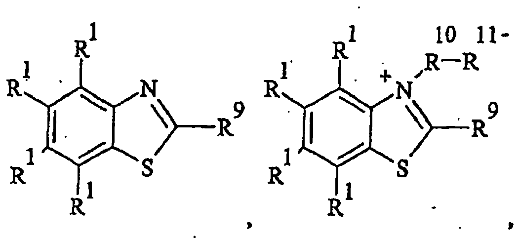
- Component A) may comprise a benzothiazole derivative.
- the benzothiazole derivative may have a formula selected from: or a combination thereof.
- R 1 is as described above.
- R 9 is a hydrogen atom, an alkyl group of 1 to 6 carbon atoms, -SH, -SCH 2 CH 2 CH 2 SO 3 Na, -NH 2 , -NHCH 3 , or -N(CH 3 ) 2 .
- R 10 is an alkyl group of 1 to 6 carbon atoms, alkenyl, or carboxyalkyl.
- R 11 is an anion comprising a halogen atom or sulfate. Examples of benzothiazole derivates are disclosed in U.S. Patent Publication 2004/0170848 A1 .
- Component A) may comprise a dialkyldithiocarbamic acid.
- the dialkyldithiocarbamic acid may have the formula: In the formula above, R 12 and R 13 are independently a hydrogen atom, an alkyl group of 1 to 6 carbon atoms, R 14 is -S- or -SCH 2 CH 2 CH 2 SO 3 -, and R 15 is a hydrogen atom, ammonium, sodium, or potassium.
- dialkyldithiocarbamic acids are disclosed in U.S. Patent Publication 2004/0170848 A1 .
- suitable thio compounds are disclosed in U.S. Patent Publication 2004/0170848 A1 , paragraphs [0016] to [0029]
- Component A) may comprise an o-alkylxanthic acid derivative.
- the o-akylxanthic acid derivative may have the formula: In the formula above, R 14 and R 15 are as described above and R 16 is an alkyl group of 1 to 6 carbon atoms.
- Component A) may comprise an amine salt derivative of a mercaptobenzothiazole.
- Said amine salt derivative may have the formula:
- R 19 is an alkyl or alkenyl group of 4 to 30 carbon atoms. Examples of amine salt derivatives of mercaptobenzothiazoles are disclosed in U.S. Patent 3,966,623 .
- Component A) may comprise a 2,5-bis-hydrocarbyldithio-1,3,4-thiadiazole.
- the 2,5-bis-hydrocarbyldithio-1,3,4-thiadiazole may have the formula:
- R 20 and R 21 are each independently alkyl groups of 4 to 30 carbon atoms or alkenyl groups of 4 to 30 carbon atoms. Examples of 2,5-bis-hydrocarbyldithio-1,3,4-thiadiazoles are disclosed in U.S. Patent 3,966,623 .
- Component A) may comprise a mercaptothiazol.
- the mercaptothiazol may have the formula:
- R 22 and R 23 are each independently selected from a hydrogen atom and an alkyl group. Examples of mercaptothiazols are disclosed in U.S. Patent 2,708,660 .
- Component A) may comprise an imidazoline.
- the imidazoline may have the formula: In the formula above, each R 24 is independently a hydrogen atom or an alkyl group, R 25 is group having a molecular weight less than 75, and R 26 is a hydrocarbon group of 8 to 20 carbon atoms. Examples of imidazolines are disclosed in U.S. Patent 2,708,660 .
- heterocyclic aromatic compounds suitable for use as component A) are exemplified by, but not limited to: acridine, 2-amino-thiazole, 2-amino-thiazoline, 2-amino-1,2-4 triazole, benzimidazole, (2-benzimidazolylthio)succinic acid, benzoxazole (and derivatives thereof), benzothiazole (and derivatives thereof), benzimidazole (and derivatives thereof), benzotriazole (BTA), 3-benzylamino-1-butyne, decamethylene imide, diaminoheptane, dicyandiamine, N,N-di-(2-ethylhexyl)-4-methyl-1H-benzotriazole-1-methanamine, 2,5-dimercapto-1,3,4 thiadiazole, dipropargyl ether, dipropargyl thioether, 6-N-ethyl purine, 1-ethylamino-2-
- Examples of compounds that may be used as component A) are disclosed in U.S. Patents 2,963,433 ; 3,966,623 ; 4,612,049 ; 5,008,153 ; 5,173,130 ; 6,583,201 and U.S. Patent Application Publication 2004/0170848 .
- Compounds suitable for use as component A) are known in the art and are commercially available. Examples include compounds supplied by CIBA® Speciality Chemicals as IRGAMET® 30 or IRGAMET® 39; R. T. Vanderbilt as CUVAN® 826 and CUVAN® 484; and Rhein Chemie Group as Additin® 8210, 8213, 8221, 8239 series.
- CIBA® Speciality Chemicals as IRGAMET® 30 or IRGAMET® 39
- R. T. Vanderbilt as CUVAN® 826 and CUVAN® 484
- Rhein Chemie Group as Additin® 8210, 8213, 8221, 8239 series.
- Component B) is an organosilane.
- the amount of organosilane added to the electromigration resistant composition may be 50 % to 90 % based on the combined weights of components A), B), and C).
- the organosilane may be, for example, an alkoxysilane, an amino alkyl silane, an epoxy alkyl silane, a mercapto alkyl silane, or a combination thereof.
- alkoxysilanes include 2-methoxy-1-methylethylorthosilicate, tetraethyl orthosilicate, tetrapropyl orthosilicate, and a combination thereof.
- amino alkyl silanes include gamma-aminopropyltriethoxysilane, aminopropyltrimethoxysilane, N-beta(aminoethyl)-gamma-aminopropyltrimethoxysilane.
- mercapto alkyl silanes include, but are not limited to, gamma-mercaptopropyltrimethoxysilane.
- organosilanes suitable for use as component B) are disclosed in U.S. Patent 5,008,153 and the references cited therein.
- the electromigration resistant composition may comprise a reaction product of components A) and B) in addition to, or instead of, all or a portion of components A) and B).
- Optional component C) is a catalyst that may be added to the electromigration resistant composition to facilitate condensation reaction.
- the catalyst may comprise a Lewis acid; a primary, secondary, or tertiary organic amine; a metal oxide; a titanium compound; a tin compound; a zirconium compound; or a combination thereof.
- Suitable catalysts are known in the art and are exemplified by the catalysts described in U.S. Patent 4,753,977 at col. 4, line 35 to col. 5, line 57.
- the amount of component C) depends on various factors including the type of catalyst selected and the choice of the remaining components in the electromigration resistant composition, however the amount of component C) may be 0 % to 50 % based on the combined weights of components A), B) and C).
- Component C) may comprise a titanium catalyst.
- Suitable titanium catalysts include organofunctional titanates, siloxytitanates, and combinations thereof.
- Organofunctional titanates are exemplified by 1,3-propanedioxytitanium bis(ethylacetoacetate); 1,3-propanedioxytitanium bis(acetylacetonate); diisopropoxytitanium bis(acetylacetonate); 2,3-di-isopropoxy-bis(ethylacetate)titanium; titanium naphthenate; tetrapropyltitanate; tetrabutyltitanate; tetraethylhexyltitanate; tetraphenyltitanate; tetraoctadecyltitanate; tetrabutoxytitanium; tetraisopropoxytitanium; ethyltriethanolaminetitanate;
- organofunctional titanates are exemplified by those in U.S. Patent 4,143,088 at col. 7, line 15 to col. 10, line 35.
- Siloxytitanates are exemplified by tetrakis(trimethylsiloxy)titanium, bis(trimethylsiloxy)bis(isopropoxy)titanium, or a combination thereof.
- the catalyst may comprise a tin compound.
- Suitable tin compounds are exemplified by dibutyltindilaurate; dibutyltindiacetate; dibutyltindimethoxide; carbomethoxyphenyl tin tris-uberate; tin octoate; isobutyl tin triceroate; dimethyl tin dibutyrate; dimethyl tin dineodeconoate; triethyl tin tartrate; dibutyl tin dibenzoate; tin oleate; tin naphthenate; butyltintri-2-ethylhexoate; tin butyrate; or a combination thereof.
- the catalyst may comprise a zirconium compound. Suitable zirconium compounds are exemplified by zirconium octoate.
- Optional component D) is a carrier that may be added to the electromigration resistant composition for ease of preparation or application of the electromigration resistant composition.
- the amount of carrier added to the electromigration resistant composition may be 0 % to 99 % based on the weight of the electromigration resistant composition.
- the carrier may be a liquid capable of wetting the substrate in step 1) and the electronic circuitry in step 2) of the process described above.
- Suitable carriers are exemplified by polar solvents such as water, alcohol, or a combination thereof. Examples of suitable alcohols include ethanol, methanol, isopropanol, butanol, and glycol ether such as propylene glycol monobutyl ether.
- the carrier may comprise a hydrocarbon such as naphtha.
- the carrier may comprise a silicone oil. Examples of carriers suitable for use as component D) are disclosed in U.S. Patent 5,008,153 .
- the electromigration resistant composition of this invention may be prepared by any conventional means, such as mixing all components at ambient temperature.
- the electromigration resistant composition of this invention is free of the film-formers disclosed in U.S. Patent Application Publication 2004/01708848 and U.S. Patent 4,612,049 .
- 'Free of film-formers' means that the electromigration resistant composition contains no film-formers or an amount of film-formers that does not interfere with the intended use of the electronic circuitry, e.g ., when the electromigration resistant composition is between Ag traces and an encapsulant, ACA, or ACF.
- FIG 1 is a portion of a PDP made using the process described above.
- the PDP includes a front sheet of glass (1) and a back sheet of glass (2).
- Ag electrodes (3) are applied to one or both sheets of glass (1), (2).
- the body of the PDP contains a dielectric layer (4) covering a portion of the Ag electrodes (3).
- the edges of the Ag electrodes (3) are kept bare to enable electrical contact between the Ag electrodes (3) and the flexible circuit tape (not shown).
- the flexible circuit tape is attached to the Ag electrodes (3) by the ACF (6).
- Application of the electromigration resistant composition to form an electromigration resistant layer (5) between the tips of the Ag electrodes (3) and the ACF (6) can reduce the occurrence of electromigration.
- Water drop testing involves applying a drop of de-ionized water to the gap between electrodes at relatively low voltages; 2 volts was used in these examples.
- the electrode patterns are those used in SIR (surface insulations resistance).
- the water drop can be viewed under an optical microscope, and the time it takes for a short to form between the conductors is measured by the increase in current. A current limit is set to avoid damaging the power supply. This test is described in Mercado, L.L., White, J., Sarihan, V.& Lee, T.T. "Failure mechanism study of ACF packages.” IEEE Trans. Comp. Hybrids & Man. Tech. 2003, 26(3) 509 .
- each composition was coated on a circuit board (P-IPC-B-25-1 from Diversified Systems of Indianapolis, Indiana, U.S.A.) having a 6.25 mil gap between Ag electrodes.
- a 3 microliter drop of de-ionized water purified via ion exchange was used, at room temperature with a 2 volts DC bias for a maximum of 1000 seconds. The drop can be limited to a 2.54 mm square area by solder mask.
- the intent of the experiment was to induce the ionic impurities on the surface to increase the strength of the electrolyte and promote silver migration. Time for the current to reach 1 Amp was recorded.
- Samples of electromigration resistant compositions are prepared by mixing the ingredients in Table 1.
- the Primer contained (C) 5 parts tetrabutoxy titanate, (B) 5 parts 2-methyoxy-1-methylethylorthosilicate, (B) 5 parts tetrapropyl orthosilicate, and 85 parts octamethyltrisiloxane.
- MBT was mercaptobenzothiazole.
- IRGAMET® 39 was N,N-bis(2-ethylhexyl)-ar-methyl-1H-benzotriazole-1-methanamine purchased from CUBA® Specialty Chemicals.
- BTA was benzotriazole.
- CUVAN® 484 was an alkylthiadiazole commercially available from R.T.
- CUVAN® 826 was a 2,5-cimercapto-1,3,4-thiadiazole derivative also available from R.T. Vanderbilt Company. 6-HQ was 6-hydroxyquinone.
- IRGAMET® 30 was a triazole derivative also from CIBA® Specialty Chemicals. 2-MB was 2-mercaptobenzimidazole.
- COBRATEC® CBT was carboxybenzotriazole from PMC Specialties Group, Inc. of Cincinnati, Ohio, U.S.A. ERA meant electromigration resistant agent.
- ERA Weight % of ERA in the total composition Time to reach 1 Amp (sec) Comparative 1 None 0 90 Comparative 2 None 0 530 3 MBT 1% 700 4 IRGAMET® 39 0.5% > 1000 5 BTA 0.5% > 1000 6 CUVAN® 484 0.5% 530 7 CUVAN® 484 1% > 1000 8 CUVAN® 826 0.5% 630 9 CUVAN® 826 1% > 1000 10 6-HQ 0.5% 850 11 2-MB 0.5% > 1000 12 COBRATEC® CBT 0.5% 630 13 Vanlube 601 0.5% 710
- the process and electromigration resistant composition of this invention reduces electromigration of Ag in electronic devices, thereby reducing failures of the devices due to short circuits. Without wishing to be bound by theory, it is thought that the process and electromigration resistant composition of this invention may also reduce corrosion.
- the process of this invention is useful during fabrication of an electronic device having electronic circuitry that is close together, such as resistors, capacitors, and displays, e.g ., a PDP or LCD.
- the process of this invention may be used during fabrication of PDP devices such as those disclosed in U.S. Patent Application Publication 2005/0062417A1 to minimize electromigration of Ag that can cause short circuits in, for example, a plasma display television.
- Figure 1 is a portion of a plasma display panel (PDP).
- PDP plasma display panel
Landscapes
- Engineering & Computer Science (AREA)
- Chemical & Material Sciences (AREA)
- Manufacturing & Machinery (AREA)
- Materials Engineering (AREA)
- Physics & Mathematics (AREA)
- Plasma & Fusion (AREA)
- Wood Science & Technology (AREA)
- Organic Chemistry (AREA)
- Life Sciences & Earth Sciences (AREA)
- Microelectronics & Electronic Packaging (AREA)
- Compositions Of Macromolecular Compounds (AREA)
- Internal Circuitry In Semiconductor Integrated Circuit Devices (AREA)
- Devices For Indicating Variable Information By Combining Individual Elements (AREA)
- Adhesives Or Adhesive Processes (AREA)
- Laminated Bodies (AREA)
Abstract
Description
- This invention relates to a process for minimizing electromigration of silver (Ag). More particularly, this invention relates to a process for minimizing electromigration of Ag in electronic circuitry. The process is useful during fabrication of an electronic device having electronic circuitry that is close together, such as resistors, capacitors, and displays, e.g., a plasma display panel (PDP) or a liquid crystal display (LCD).
- Under the influence of an applied electrical field, temperature, and humidity, Ag (either in a metallic form, or as an alloy such as CuAg, AgPd, or SnAg) may be converted to Ag+ ions, migrate, and re-deposit to form a new Ag metallic area. In an electronic device, this new Ag metallic area often takes the form of dendrites or "whiskers", which short circuit conducting Ag traces. Electromigration requires four conditions: a mobile metal; a voltage gradient; humidity or a continuous film of water; and soluble ions. Ag migration is a problem because Ag is anodically soluble and requires low activation energy to initiate the electromigration process.
- Two trends in the electronic industry are making electromigration of Ag an even more severe problem: one is the reduction in lead (Pb) in solder; the second is the continual miniaturization of circuitry. The Pb replacement solders contain increasing amounts of Ag metal, hence the greater opportunity for Ag migration. The reduction in circuitry dimensions means smaller separation between circuit elements resulting in higher electrical field gradients (Volts/m) driving the electromigration under both AC and DC conditions and increasing the potential for short circuits.
- It is known that a soluble ionic species is essential to provide the ionically conducting pathway for the Ag migration to occur, and the nature of the ionic contaminants has a major impact on the severity of Ag migration. High ionic mobility is influenced by such factors as ionic radius, electro-negativity, electron affinity, and charge to size. The source of these ions is varied, but can usually be traced to the substrate, or residues of the circuitry fabrication process. High polarity and hydrophilic substrates such as glass and some epoxy substrates are particularly susceptible to Ag migration especially when exposed to high humidity and temperature.
US 6,773,757 discloses a method of treating silver plate with an alkaline polymer coating. The polymer coating does not include an organosilane. - This invention relates to a process for reducing electromigration in electronic circuitry. The process comprises treating the electronic circuitry with an electromigration resistant composition. This invention further relates to a process for producing a PDP
- All amounts, ratios, and percentages are by weight unless otherwise indicated. The following is a list of definitions as used herein.
- "A" and "an" each mean one or more.
- "Corrosion" means a process by which a metal oxidizes or becomes alloyed in the presence or absence of an applied electrical field.
- "Electromigration" means the transport of a metal on a nonmetallic medium under the influence of an applied electrical field.
- This invention relates to a process comprising:
- 1) forming electronic circuitry on a substrate,
- 2) treating all or a portion of the electronic circuitry with an electromigration resistant composition, and
optionally 3) coating the product of step 2). - The electronic circuitry comprises Ag electrodes, such as address electrodes, display electrodes, and scanning electrodes useful in a PDP. The electrodes may be bare or coated. The electronic circuitry may be formed by any conventional means.
- The substrate used in this process is not specifically restricted. The substrate selected will depend on the various factors including the use of the process described above, e.g., the type of electronic device to be fabricated. The substrate can be any material used in the fabrication of an electronic device. The substrate can be, for example a ceramic substrate, a flexible substrate, or a rigid substrate commonly used in electronic device packaging. Examples of suitable substrates include glass, a ceramic, a metal, a metal-coated surface, a polymer, and combinations thereof.
- Metals and metal coatings include aluminum, chromium, copper, gold, lead, nickel, platinum, solder, stainless steel, tin, titanium, alloys thereof, and combinations thereof.
- Ceramics include aluminum nitride, aluminum oxide, silicon carbide, silicon oxide, silicon oxynitride, and combinations thereof.
- Polymers include benzocyclobutene, bismaleimide, cyanate, epoxy, polybenzoxazole, polycarbonate, polyimide, polymethylmethacrylate, polyphenylene ether, polyvinylidene chloride, and combinations thereof.
- Without wishing to be bound by theory it is thought that treating in step 2) provides an interface between the electronic circuitry and subsequent coatings that may be applied in step 3). The electronic circuitry may be treated by any conventional means such as dipping, spraying, flow coating, roll coating, wiping, or spin coating.
- In optional step 3), the treated electronic circuitry from step 2) may be coated with, for example, an encapsulant, a conductive film, a conductive adhesive, or a combination thereof. The encapsulant may be thermally cured, radiation cured, or aerobically cured (e.g., moisture cured). The encapsulant may be an epoxy, silicone, urethane, or acrylic. The conductive film may be an anisotropically conductive film (ACF). The adhesive may be an anisotropically conductive adhesive (ACA). The electromigration resistant composition should not detrimentally affect performance of such encapsulant, ACF, or ACA.
- The electromigration resistant composition comprises:
- A) an electromigration resistant agent,
- B) an organosilane,
optionally - C) a catalyst, and
- D) a carrier.
- The amount of component A) will depend on the choice of electromigration resistant agent or agents selected for component A), the choice of organosilane or organosilanes for component B), the choice of catalyst or catalysts, if any, for component C), and the choice of carrier or carriers, if any, for component D). However, the amount of component A) in the electromigration resistant composition may range from 1 % to 50 % based on the combined weights of components A), B), and C). Alternatively, the composition may contain 0.01 % to 50 %, alternatively 0.01 % to 5 %, and alternatively 0.01 % to 0.5 %, based on the total weight of the composition.
- Component A) may comprise a heterocyclic aromatic compound. The heterocyclic aromatic compound may comprise a nitrogen atom or a sulfur atom in a ring. The heterocyclic aromatic compounds containing a nitrogen atom in a ring may have a substituted or unsubstituted five-membered ring. The ring may be substituted with mercapto, amino, or carboxyl groups.
- Component A) may comprise an aliphatic or cycloaliphatic mono- or polycarboxylic acid substituted in its aliphatic or cycloaliphatic group by at least one group of formula:

U.S. Patent 4,612,049 at col. 4, line 20 to col. 10, line 34, which is hereby incorporated by reference. - Component A) may comprise a thiourea derivative. The thiourea derivative may have a formula selected from:

In the formula above, each R4, R5, and R6 are independently selected from a hydrogen atom, an alkyl group of 1 to 6 carbon atoms, acetyl, and alkenyl. R7 is hydrogen, an alkyl group of 1 to 6 carbon atoms, acetyl, alkenyl, or -NH2. R8 is a divalent hydrocarbon group of at least two carbon atoms such as ethylene, n-propylene, or isopropylene. Examples of thiourea derivatives are disclosed inU.S. Patent Publication 2004/0170848 A1. - Component A) may comprise a benzothiazole derivative. The benzothiazole derivative may have a formula selected from:

In the formulae above, R1 is as described above. R9 is a hydrogen atom, an alkyl group of 1 to 6 carbon atoms, -SH, -SCH2CH2CH2SO3Na, -NH2, -NHCH3, or -N(CH3)2. R10 is an alkyl group of 1 to 6 carbon atoms, alkenyl, or carboxyalkyl. R11 is an anion comprising a halogen atom or sulfate. Examples of benzothiazole derivates are disclosed inU.S. Patent Publication 2004/0170848 A1 . - Component A) may comprise a dialkyldithiocarbamic acid. The dialkyldithiocarbamic acid may have the formula:
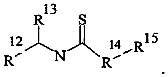
U.S. Patent Publication 2004/0170848 A1 . Examples of suitable thio compounds are disclosed inU.S. Patent Publication 2004/0170848 A1 , paragraphs [0016] to [0029] - Component A) may comprise an o-alkylxanthic acid derivative. The o-akylxanthic acid derivative may have the formula:

- Component A) may comprise a heterocyclic compound of the formula:

U.S. Patent 2,963,433 . - Component A) may comprise an amine salt derivative of a mercaptobenzothiazole. Said amine salt derivative may have the formula:

U.S. Patent 3,966,623 . - Component A) may comprise a 2,5-bis-hydrocarbyldithio-1,3,4-thiadiazole. The 2,5-bis-hydrocarbyldithio-1,3,4-thiadiazole may have the formula:

U.S. Patent 3,966,623 . - Component A) may comprise a mercaptothiazol. The mercaptothiazol may have the formula:

U.S. Patent 2,708,660 . Component A) may comprise an imidazoline. The imidazoline may have the formula: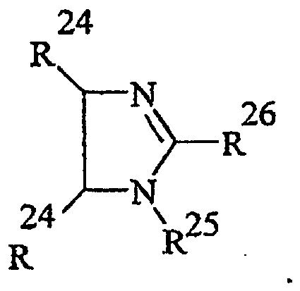
U.S. Patent 2,708,660 . - Examples of suitable heterocyclic aromatic compounds suitable for use as component A) are exemplified by, but not limited to: acridine, 2-amino-thiazole, 2-amino-thiazoline, 2-amino-1,2-4 triazole, benzimidazole, (2-benzimidazolylthio)succinic acid, benzoxazole (and derivatives thereof), benzothiazole (and derivatives thereof), benzimidazole (and derivatives thereof), benzotriazole (BTA), 3-benzylamino-1-butyne, decamethylene imide, diaminoheptane, dicyandiamine, N,N-di-(2-ethylhexyl)-4-methyl-1H-benzotriazole-1-methanamine, 2,5-dimercapto-1,3,4 thiadiazole, dipropargyl ether, dipropargyl thioether, 6-N-ethyl purine, 1-ethylamino-2-quinoline (and derivatives thereof), hexamethylene-3,5-dinitrobenzene, hexamethylene imide, hexamethylene iminebenzoate, hexamethylene tetramine, imidazole (and derivatives thereof, 3-isopropylamino-1-butyne, mercaptan, mercaptobenzothiazole (MBT), 2-mercaptothiazoline, d-oximino-b-vinyl quinuclidine 1,10-phenathiodine, phenanthroline, phenothiazine, propargyl quinolinium bromide, propargyl caproate, (2-thio-2'-benzo-thiazolyl) butanedioic acid, thiophenol (and derivatives thereof), toluidine, and combinations thereof.
- Examples of compounds that may be used as component A) are disclosed in
U.S. Patents 2,963,433 ;3,966,623 ;4,612,049 ;5,008,153 ;5,173,130 ;6,583,201 andU.S. Patent Application Publication 2004/0170848 . Compounds suitable for use as component A) are known in the art and are commercially available. Examples include compounds supplied by CIBA® Speciality Chemicals as IRGAMET® 30 or IRGAMET® 39; R. T. Vanderbilt as CUVAN® 826 and CUVAN® 484; and Rhein Chemie Group as Additin® 8210, 8213, 8221, 8239 series. One skilled in the art would recognize that a single compound described above or a combination comprising two or more of the above compounds that differ in structure may be used as component A). - Component B) is an organosilane. The amount of organosilane added to the electromigration resistant composition may be 50 % to 90 % based on the combined weights of components A), B), and C). The organosilane may be, for example, an alkoxysilane, an amino alkyl silane, an epoxy alkyl silane, a mercapto alkyl silane, or a combination thereof. Examples of alkoxysilanes include 2-methoxy-1-methylethylorthosilicate, tetraethyl orthosilicate, tetrapropyl orthosilicate, and a combination thereof. Examples of amino alkyl silanes include gamma-aminopropyltriethoxysilane, aminopropyltrimethoxysilane, N-beta(aminoethyl)-gamma-aminopropyltrimethoxysilane. Examples of mercapto alkyl silanes include, but are not limited to, gamma-mercaptopropyltrimethoxysilane. Examples of organosilanes suitable for use as component B) are disclosed in
U.S. Patent 5,008,153 and the references cited therein. Alternatively, the electromigration resistant composition may comprise a reaction product of components A) and B) in addition to, or instead of, all or a portion of components A) and B). - Optional component C) is a catalyst that may be added to the electromigration resistant composition to facilitate condensation reaction. The catalyst may comprise a Lewis acid; a primary, secondary, or tertiary organic amine; a metal oxide; a titanium compound; a tin compound; a zirconium compound; or a combination thereof. Suitable catalysts are known in the art and are exemplified by the catalysts described in
U.S. Patent 4,753,977 at col. 4, line 35 to col. 5, line 57. The amount of component C) depends on various factors including the type of catalyst selected and the choice of the remaining components in the electromigration resistant composition, however the amount of component C) may be 0 % to 50 % based on the combined weights of components A), B) and C). - Component C) may comprise a titanium catalyst. Suitable titanium catalysts include organofunctional titanates, siloxytitanates, and combinations thereof. Organofunctional titanates are exemplified by 1,3-propanedioxytitanium bis(ethylacetoacetate); 1,3-propanedioxytitanium bis(acetylacetonate); diisopropoxytitanium bis(acetylacetonate); 2,3-di-isopropoxy-bis(ethylacetate)titanium; titanium naphthenate; tetrapropyltitanate; tetrabutyltitanate; tetraethylhexyltitanate; tetraphenyltitanate; tetraoctadecyltitanate; tetrabutoxytitanium; tetraisopropoxytitanium; ethyltriethanolaminetitanate; a betadicarbonyltitanium compound such as bis(acetylacetonyl)diisopropyltitanate; or a combination thereof. Other organofunctional titanates are exemplified by those in
U.S. Patent 4,143,088 at col. 7, line 15 to col. 10, line 35. Siloxytitanates are exemplified by tetrakis(trimethylsiloxy)titanium, bis(trimethylsiloxy)bis(isopropoxy)titanium, or a combination thereof. - The catalyst may comprise a tin compound. Suitable tin compounds are exemplified by dibutyltindilaurate; dibutyltindiacetate; dibutyltindimethoxide; carbomethoxyphenyl tin tris-uberate; tin octoate; isobutyl tin triceroate; dimethyl tin dibutyrate; dimethyl tin dineodeconoate; triethyl tin tartrate; dibutyl tin dibenzoate; tin oleate; tin naphthenate; butyltintri-2-ethylhexoate; tin butyrate; or a combination thereof.
- The catalyst may comprise a zirconium compound. Suitable zirconium compounds are exemplified by zirconium octoate.
- Optional component D) is a carrier that may be added to the electromigration resistant composition for ease of preparation or application of the electromigration resistant composition. The amount of carrier added to the electromigration resistant composition may be 0 % to 99 % based on the weight of the electromigration resistant composition. The carrier may be a liquid capable of wetting the substrate in step 1) and the electronic circuitry in step 2) of the process described above. Suitable carriers are exemplified by polar solvents such as water, alcohol, or a combination thereof. Examples of suitable alcohols include ethanol, methanol, isopropanol, butanol, and glycol ether such as propylene glycol monobutyl ether. Alternatively, the carrier may comprise a hydrocarbon such as naphtha. Alternatively, the carrier may comprise a silicone oil. Examples of carriers suitable for use as component D) are disclosed in
U.S. Patent 5,008,153 . - The electromigration resistant composition of this invention may be prepared by any conventional means, such as mixing all components at ambient temperature.
- The electromigration resistant composition of this invention is free of the film-formers disclosed in
U.S. Patent Application Publication 2004/01708848 U.S. Patent 4,612,049 . 'Free of film-formers' means that the electromigration resistant composition contains no film-formers or an amount of film-formers that does not interfere with the intended use of the electronic circuitry, e.g., when the electromigration resistant composition is between Ag traces and an encapsulant, ACA, or ACF. - These examples are intended to illustrate the invention to one of ordinary skill in the art and should not be interpreted to limit the scope of the invention set forth in the claims.
-
Figure 1 is a portion of a PDP made using the process described above. The PDP includes a front sheet of glass (1) and a back sheet of glass (2). Ag electrodes (3) are applied to one or both sheets of glass (1), (2). The body of the PDP contains a dielectric layer (4) covering a portion of the Ag electrodes (3). The edges of the Ag electrodes (3) are kept bare to enable electrical contact between the Ag electrodes (3) and the flexible circuit tape (not shown). The flexible circuit tape is attached to the Ag electrodes (3) by the ACF (6). Application of the electromigration resistant composition to form an electromigration resistant layer (5) between the tips of the Ag electrodes (3) and the ACF (6) can reduce the occurrence of electromigration. - Water drop testing involves applying a drop of de-ionized water to the gap between electrodes at relatively low voltages; 2 volts was used in these examples. The electrode patterns are those used in SIR (surface insulations resistance). The water drop can be viewed under an optical microscope, and the time it takes for a short to form between the conductors is measured by the increase in current. A current limit is set to avoid damaging the power supply. This test is described in Mercado, L.L., White, J., Sarihan, V.& Lee, T.T. "Failure mechanism study of ACF packages." IEEE Trans. Comp. Hybrids & Man. Tech. 2003, 26(3) 509.
- In these examples, each composition was coated on a circuit board (P-IPC-B-25-1 from Diversified Systems of Indianapolis, Indiana, U.S.A.) having a 6.25 mil gap between Ag electrodes. A 3 microliter drop of de-ionized water purified via ion exchange was used, at room temperature with a 2 volts DC bias for a maximum of 1000 seconds. The drop can be limited to a 2.54 mm square area by solder mask. The intent of the experiment was to induce the ionic impurities on the surface to increase the strength of the electrolyte and promote silver migration. Time for the current to reach 1 Amp was recorded.
- Samples of electromigration resistant compositions are prepared by mixing the ingredients in Table 1. The Primer contained (C) 5 parts tetrabutoxy titanate, (B) 5 parts 2-methyoxy-1-methylethylorthosilicate, (B) 5 parts tetrapropyl orthosilicate, and 85 parts octamethyltrisiloxane. MBT was mercaptobenzothiazole. IRGAMET® 39 was N,N-bis(2-ethylhexyl)-ar-methyl-1H-benzotriazole-1-methanamine purchased from CUBA® Specialty Chemicals. BTA was benzotriazole. CUVAN® 484 was an alkylthiadiazole commercially available from R.T. Vanderbilt Company of Norwalk, Connecticut, U.S.A. CUVAN® 826 was a 2,5-cimercapto-1,3,4-thiadiazole derivative also available from R.T. Vanderbilt Company. 6-HQ was 6-hydroxyquinone. IRGAMET® 30 was a triazole derivative also from CIBA® Specialty Chemicals. 2-MB was 2-mercaptobenzimidazole. COBRATEC® CBT was carboxybenzotriazole from PMC Specialties Group, Inc. of Cincinnati, Ohio, U.S.A. ERA meant electromigration resistant agent.
- The electromigration resistant compositions of examples 3-13 were each coated on a circuit board. For comparison, an uncoated circuit board (Ex. 1) and a circuit board coated with a primer without an electromigration resistant agent (Ex. 2) were tested according to the method in reference example 2. The results are in Table 1. The results show that each electromigration resistant agent tested lengthened the time before failure (current reaching 1 Amp). One skilled in the art would be able to optimize the amount of electromigration resistant agent without undue experimentation.
Table 1 Example No. ERA Weight % of ERA in the total composition Time to reach 1 Amp (sec) Comparative 1None 0 90 Comparative 2None 0 530 3 MBT 1% 700 4 IRGAMET® 39 0.5% > 1000 5 BTA 0.5% > 1000 6 CUVAN® 484 0.5% 530 7 CUVAN® 484 1% > 1000 8 CUVAN® 826 0.5% 630 9 CUVAN® 826 1% > 1000 10 6-HQ 0.5% 850 11 2-MB 0.5% > 1000 12 COBRATEC® CBT 0.5% 630 13 Vanlube 601 0.5% 710 - The process and electromigration resistant composition of this invention reduces electromigration of Ag in electronic devices, thereby reducing failures of the devices due to short circuits. Without wishing to be bound by theory, it is thought that the process and electromigration resistant composition of this invention may also reduce corrosion. The process of this invention is useful during fabrication of an electronic device having electronic circuitry that is close together, such as resistors, capacitors, and displays, e.g., a PDP or LCD. The process of this invention may be used during fabrication of PDP devices such as those disclosed in
U.S. Patent Application Publication 2005/0062417A1 to minimize electromigration of Ag that can cause short circuits in, for example, a plasma display television. -
Figure 1 is a portion of a plasma display panel (PDP). -
- 1. front glass
- 2. back glass
- 3. silver electrodes
- 4. dielectric layer
- 5. anti migration layer
- 6. ACF, asymmetrically conductive adhesive
Claims (8)
- A process for minimizing electromigration of Ag in electronic circuitry comprising:1) forming the electronic circuitry on a substrate, the electronic circuitry comprising Ag electrodes,2) treating all or a portion of the electronic circuitry with an electromigration resistant composition, where the electromigration resistant composition comprisesA) an electromigration resistant agent,B) an organosilane,
optionallyC) a catalyst, andD) a carrier, and
optionally3) coating the product of step 2). - The process of claim 1, where step 3) is present and the product of step 2) is coated with a coating selected from an encapsulant, a conductive film, a conductive adhesive, or a combination thereof.
- The process of claim 2 wherein the coating is an anisotropically conductive film.
- a process according to claim 1 for fabricating a plasma display panel comprising:1) forming Ag electrodes on a glass panel,2) treating the Ag electrodes with an electromigration resistant composition where the electromigration resistant composition comprisesA) an electromigration resistant agent,B) an organosilane,
optionallyC) a catalyst andD) a carrier selected from the group consisting of a hydrocarbon, silicone oil, or a combination thereof, and3) coating the product of step 2). - The process of any of claims 1 to 4 where component A) is selected from acridine, 2-amino-thiazole, 2-amino-thiazoline, 2-amino-1,2-4 triazole, benzimidazole, (2-benzimidazolylthio)succinic acid, benzoxazole (and derivatives thereof), benzothiazole (and derivatives thereof), benzimidazole (and derivatives thereof), benzotriazole, 3-benzylamino-1-butyne, decamethylene imide; diaminoheptane, dicyandiamine, N,N-di-(2-ethylhexyl)-4-methyl-1H-benzotriazole-1-methanamine, 2,5-dimercapto-1,3,4 thiadiazole, dipropargyl ether, dipropargyl thioether, 6-N-ethyl purine, 1-ethylamino-2-quinoline (and derivatives thereof), hexamethylene-3,5-dinitrobenzene, hexamethylene imide, hexamethylene iminebenzoate, hexamethylene tetramine, imidazole (and derivatives thereof), 3-isopropylamino-1-butyne, mercaptan, mercaptobenzothiazole, 2-mercaptothiazoline, d-oximino-b-vinyl quinnolidine 1,10-phenathiodine, phenanthroline, phenothiazine, propargyl quinolinium bromide, propargyl caproate, (2-thio-2'-benzothiazolyl) butanedioic acid, thiophenol (and derivatives thereof), toluidine, or a combination thereof.
- The process of any of claims 1 to 4 where component A) is selected from:I) an aliphatic or cycloaliphatic mono- or poly- carboxylic acid substituted in its aliphatic or cycloaliphatic group by at least one group of formula:
 II) a thiourea derivative having a formula selected from:
 III) a beazothiazole derivative having a formula selected from:
 IV) a dialkyldithiocarbamic acid having formula:
 V) an o-alkylxanthic acid derivative having formula:
 VI) a.heterocyclic compound having formula:
 VII) an amine salt derivative of a mercaptobenzothiazole having formula:
 VIII) a 2,5-bis-hydrocarbyldithio-1,3,4-thiadiazole having formula:
 IX) a mercaptothiazol having formula:
 X) an imidazoline having formula:
- The process of any of claims 1 to 4, where component B) comprises an alkoxysilane, an amino alkyl silane, an epoxy alkyl silane, a mercapto alkyl silane, or a combination thereof.
- The process of any of claims 1, to 4 where component C) is present and comprises a catalyst selected from a Lewis acid; a primary, secondary, or tertiary organic amine; a metal oxide; a titanium compound; a tin compound; a zirconium compound; or a combination thereof.
Applications Claiming Priority (2)
| Application Number | Priority Date | Filing Date | Title |
|---|---|---|---|
| US67961005P | 2005-05-10 | 2005-05-10 | |
| PCT/US2006/017718 WO2006122025A1 (en) | 2005-05-10 | 2006-05-09 | Process for minimizing electromigration in an electronic device |
Publications (2)
| Publication Number | Publication Date |
|---|---|
| EP1880416A1 EP1880416A1 (en) | 2008-01-23 |
| EP1880416B1 true EP1880416B1 (en) | 2012-01-18 |
Family
ID=36917362
Family Applications (1)
| Application Number | Title | Priority Date | Filing Date |
|---|---|---|---|
| EP06770087A Expired - Lifetime EP1880416B1 (en) | 2005-05-10 | 2006-05-09 | Process for minimizing electromigration in an electronic device |
Country Status (6)
| Country | Link |
|---|---|
| US (1) | US8450931B2 (en) |
| EP (1) | EP1880416B1 (en) |
| JP (1) | JP5107236B2 (en) |
| KR (1) | KR101216577B1 (en) |
| AT (1) | ATE542239T1 (en) |
| WO (1) | WO2006122025A1 (en) |
Families Citing this family (7)
| Publication number | Priority date | Publication date | Assignee | Title |
|---|---|---|---|---|
| FR2911341B1 (en) * | 2007-01-11 | 2013-01-11 | Ascotec | CORROSION INHIBITOR |
| KR20080108767A (en) * | 2007-06-11 | 2008-12-16 | 삼성에스디아이 주식회사 | Electrode terminal coating material and plasma display panel |
| US10475546B2 (en) * | 2013-05-30 | 2019-11-12 | National Research Council Of Canada | Conductors comprising a functionalized organosiloxane network and methods for the preparation thereof |
| KR102175447B1 (en) * | 2013-07-11 | 2020-11-06 | 세메다인 가부시키 가이샤 | Production method for electrically conductive cured article and curing method for pulsed light curing composition |
| CN106153708A (en) * | 2015-04-17 | 2016-11-23 | 北京中科纳通电子技术有限公司 | A kind of experimental technique of test touch screen silver slurry anti-silver transfer ability |
| KR101769716B1 (en) * | 2016-08-04 | 2017-08-18 | 성균관대학교산학협력단 | Electrochemical migration preventive additives and method for inhibiting electrochemical migration by using the same |
| JP2023068718A (en) * | 2021-11-04 | 2023-05-18 | コニカミノルタ株式会社 | Printed wiring boards and printed circuit boards |
Family Cites Families (43)
| Publication number | Priority date | Publication date | Assignee | Title |
|---|---|---|---|---|
| US1057871A (en) | 1912-08-10 | 1913-04-01 | Burke W Mott | Window-ventilator. |
| US2708660A (en) | 1950-07-29 | 1955-05-17 | Sun Oil Co | Soluble oil rust inhibitors |
| US2963433A (en) | 1957-12-02 | 1960-12-06 | Standard Oil Co | Lubricant composition |
| US3649373A (en) | 1970-01-29 | 1972-03-14 | Schering Ag | Passivating agent for protecting the surfaces of silver-bearing materials |
| US3966623A (en) | 1975-06-05 | 1976-06-29 | Texaco Inc. | Corrosion inhibited lube oil compositions |
| FR2345491A1 (en) | 1976-03-24 | 1977-10-21 | Rhone Poulenc Ind | ORGANOSILICIC COMPOSITIONS STABLE IN STORAGE, QUICKLY HARDENING IN THE PRESENCE OF WATER IN SELF-ADHESIVE PLASTOMERS |
| US4306987A (en) | 1979-11-19 | 1981-12-22 | Basf Wyandotte Corporation | Low-foaming nonionic surfactant for machine dishwashing detergent |
| US4623474A (en) | 1981-12-10 | 1986-11-18 | Union Oil Company Of California | Oxidation and corrosion inhibitors for boron-containing lubricants |
| US4377619A (en) * | 1981-05-08 | 1983-03-22 | Bell Telephone Laboratories, Incorporated | Prevention of surface mass migration by means of a polymeric surface coating |
| NL8204783A (en) | 1982-12-10 | 1984-07-02 | Philips Nv | METHOD FOR APPLYING A METAL LAYER ON A SUBSTRATE |
| GB8313320D0 (en) | 1983-05-14 | 1983-06-22 | Ciba Geigy Ag | Coating compositions |
| DE3405916A1 (en) | 1984-02-18 | 1985-08-22 | Robert Bosch Gmbh, 7000 Stuttgart | MIXING METERING SYSTEM FOR AN INTERNAL COMBUSTION ENGINE |
| US4753977A (en) | 1986-12-10 | 1988-06-28 | General Electric Company | Water repellent for masonry |
| US5008153A (en) | 1988-12-08 | 1991-04-16 | Ppg Industries, Inc. | Corrosion inhibitive pretreatment for "copper-free" mirrors |
| CA1321068C (en) * | 1989-08-21 | 1993-08-10 | Kenneth R. Winder | Gripping ferrule |
| EP0428383A1 (en) | 1989-11-13 | 1991-05-22 | Shikoku Chemicals Corporation | Process for surface treatment of copper and copper alloy |
| US5487792A (en) | 1994-06-13 | 1996-01-30 | Midwest Research Institute | Molecular assemblies as protective barriers and adhesion promotion interlayer |
| GB9418289D0 (en) | 1994-09-10 | 1994-10-26 | Univ Liverpool | Solutions or dispersions and a method of synthesising materials having controlled electronic and optical properties therefrom |
| US6068711A (en) | 1994-10-07 | 2000-05-30 | Mcmaster University | Method of increasing corrosion resistance of metals and alloys by treatment with rare earth elements |
| US5476552A (en) | 1995-01-25 | 1995-12-19 | The United States Of America As Represented By The Secretary Of The Navy | Surface preparation for bonding titanium |
| US5925174A (en) * | 1995-05-17 | 1999-07-20 | Henkel Corporation | Composition and process for treating the surface of copper-containing metals |
| JPH08311658A (en) | 1995-05-17 | 1996-11-26 | Nippon Parkerizing Co Ltd | Composition for surface treatment of copper-based metal material |
| KR100307839B1 (en) | 1995-07-13 | 2002-11-22 | 토넨제네랄세키유 가부시키가이샤 | Composition for forming ceramic material and manufacturing method of ceramic material |
| ATE280202T1 (en) | 1995-08-25 | 2004-11-15 | Grace Gmbh | ANTI-CORROSIVE PIGMENTS AND COMPOSITIONS CONTAINING SAME |
| AU716903B2 (en) | 1995-10-10 | 2000-03-09 | Prc-Desoto International, Inc. | Non-chromate corrosion inhibitors for aluminum alloys |
| US5773197A (en) * | 1996-10-28 | 1998-06-30 | International Business Machines Corporation | Integrated circuit device and process for its manufacture |
| US6870263B1 (en) * | 1998-03-31 | 2005-03-22 | Infineon Technologies Ag | Device interconnection |
| KR19990082911A (en) * | 1998-04-06 | 1999-11-25 | 기타지마 요시토시 | A plasma display panel and a rearplate and a method for forming the fluorescence surface thereof |
| TW387926B (en) | 1998-05-15 | 2000-04-21 | Nippon Dacro Shamrock Co | Surface treatment agent for metals, surface treatment method for metals, and pre-coated steel plate |
| US6056554A (en) | 1998-09-09 | 2000-05-02 | Samole; Sidney | Apparatus and method for finding and identifying nighttime sky objects |
| EP0988802A1 (en) | 1998-09-22 | 2000-03-29 | Fabriques De Tabac Reunies S.A. | Method for removing a blockage in a machine for the manufacturing of tobacco products and machine operating according to said method |
| KR100313706B1 (en) | 1999-09-29 | 2001-11-26 | 윤종용 | Redistributed Wafer Level Chip Size Package And Method For Manufacturing The Same |
| JP4652526B2 (en) | 2000-05-12 | 2011-03-16 | 古河電気工業株式会社 | Insulated wire |
| KR100352270B1 (en) | 2000-10-19 | 2002-09-12 | 주식회사 아이센스 | Microchip-type oxygen gas sensor based on differential potentiometry |
| WO2002040419A1 (en) | 2000-11-15 | 2002-05-23 | Saint-Gobain Glass France | Object with metallic layer, method for making same and uses |
| FR2818271B1 (en) | 2000-12-20 | 2003-08-29 | Saint Gobain | PROCESS FOR THE MANUFACTURE OF A MULTI-TOUCH PRODUCT, APPLICATION OF THE PROCESS AND USE OF AN ASSOCIATED ADHESION PROMOTER |
| US6583201B2 (en) | 2001-04-25 | 2003-06-24 | National Starch And Chemical Investment Holding Corporation | Conductive materials with electrical stability for use in electronics devices |
| JP3770194B2 (en) | 2001-04-27 | 2006-04-26 | 松下電器産業株式会社 | Plasma display panel and manufacturing method thereof |
| US6447594B1 (en) | 2001-06-13 | 2002-09-10 | Wayne Pigment Corporation | Strontium chromate corrosion inhibitor pigment with reduced solubility |
| CN100378551C (en) | 2001-10-22 | 2008-04-02 | 三星电子株式会社 | Liquid crystal display and manufacturing method thereof |
| US20040170848A1 (en) | 2003-02-28 | 2004-09-02 | Columbia Chemical Corporation | Corrosion inhibiting composition for metals |
| US6773757B1 (en) * | 2003-04-14 | 2004-08-10 | Ronald Redline | Coating for silver plated circuits |
| US7285913B2 (en) | 2003-08-29 | 2007-10-23 | Matsushita Electric Industrial Co., Ltd. | Plasma display device having blue phosphor layers with alkaline earth metal aluminate containing molybdenum or tungsten |
-
2006
- 2006-05-09 EP EP06770087A patent/EP1880416B1/en not_active Expired - Lifetime
- 2006-05-09 US US11/883,992 patent/US8450931B2/en not_active Expired - Fee Related
- 2006-05-09 AT AT06770087T patent/ATE542239T1/en active
- 2006-05-09 KR KR1020077026176A patent/KR101216577B1/en not_active Expired - Fee Related
- 2006-05-09 JP JP2008511236A patent/JP5107236B2/en not_active Expired - Fee Related
- 2006-05-09 WO PCT/US2006/017718 patent/WO2006122025A1/en not_active Ceased
Also Published As
| Publication number | Publication date |
|---|---|
| ATE542239T1 (en) | 2012-02-15 |
| JP2008541453A (en) | 2008-11-20 |
| US8450931B2 (en) | 2013-05-28 |
| WO2006122025A1 (en) | 2006-11-16 |
| WO2006122025B1 (en) | 2006-12-21 |
| KR20080017309A (en) | 2008-02-26 |
| EP1880416A1 (en) | 2008-01-23 |
| KR101216577B1 (en) | 2013-01-02 |
| JP5107236B2 (en) | 2012-12-26 |
| US20080054806A1 (en) | 2008-03-06 |
Similar Documents
| Publication | Publication Date | Title |
|---|---|---|
| US7179741B2 (en) | Electroless plating method and semiconductor wafer on which metal plating layer is formed | |
| JP3510141B2 (en) | Electroplating method | |
| TW593731B (en) | Apparatus for applying a metal structure to a workpiece | |
| CN1267891A (en) | Conducting and resistance material with electrical stability using for electronic equipment | |
| US8450931B2 (en) | Process for minimizing electromigration in an electronic device | |
| US12410524B2 (en) | Method for manufacturing laminate | |
| KR101643655B1 (en) | Solution for etching silicon oxide layer | |
| JP2008007849A (en) | Primer composition for electroless plating and electroless plating method | |
| US20260130186A1 (en) | Substrate wettability for plating operations | |
| US20100155103A1 (en) | Electrically conductive ink | |
| EP3238249B1 (en) | Method for electromagnetic shielding and thermal management of active components | |
| TWI870646B (en) | Process solution composition for polymer processing | |
| KR20010087263A (en) | Anticorrosive treating concentrate | |
| KR101558479B1 (en) | Etching composition for silicon oxide layer | |
| CN114875460B (en) | Synthesis method and application of ultrathin pore-filling copper plating leveling agent | |
| JP4809546B2 (en) | Void-free copper plating method using organic solvent | |
| CN107630238B (en) | Indium electroplating composition and method for electroplating indium | |
| US12281404B2 (en) | Tin-indium alloy electroplating solution | |
| EP4640363A1 (en) | Metal paste composition and metal-ceramic composite substrate comprising the same | |
| KR102890398B1 (en) | Etchant composition for etching silicon and silicon germanium, and preparation method of pattern using the same | |
| KR20210100923A (en) | A metal layer etchant composition and a pattern formation method using the same | |
| JPS6389695A (en) | Neutral ph electrolytic bath for electroplating | |
| CN107630236A (en) | The method of indium electroplating compositions and indium plating containing 2 imidazolidine thione compounds | |
| US20220090282A1 (en) | Manufacturing method of aluminum nitride | |
| KR20000038812A (en) | Copper foil for printed circuit and production method thereof |
Legal Events
| Date | Code | Title | Description |
|---|---|---|---|
| PUAI | Public reference made under article 153(3) epc to a published international application that has entered the european phase |
Free format text: ORIGINAL CODE: 0009012 |
|
| 17P | Request for examination filed |
Effective date: 20070912 |
|
| AK | Designated contracting states |
Kind code of ref document: A1 Designated state(s): AT BE BG CH CY CZ DE DK EE ES FI FR GB GR HU IE IS IT LI LT LU LV MC NL PL PT RO SE SI SK TR |
|
| 17Q | First examination report despatched |
Effective date: 20080208 |
|
| DAX | Request for extension of the european patent (deleted) | ||
| GRAP | Despatch of communication of intention to grant a patent |
Free format text: ORIGINAL CODE: EPIDOSNIGR1 |
|
| GRAS | Grant fee paid |
Free format text: ORIGINAL CODE: EPIDOSNIGR3 |
|
| GRAA | (expected) grant |
Free format text: ORIGINAL CODE: 0009210 |
|
| AK | Designated contracting states |
Kind code of ref document: B1 Designated state(s): AT BE BG CH CY CZ DE DK EE ES FI FR GB GR HU IE IS IT LI LT LU LV MC NL PL PT RO SE SI SK TR |
|
| REG | Reference to a national code |
Ref country code: GB Ref legal event code: FG4D |
|
| REG | Reference to a national code |
Ref country code: CH Ref legal event code: EP |
|
| REG | Reference to a national code |
Ref country code: IE Ref legal event code: FG4D Ref country code: AT Ref legal event code: REF Ref document number: 542239 Country of ref document: AT Kind code of ref document: T Effective date: 20120215 |
|
| REG | Reference to a national code |
Ref country code: DE Ref legal event code: R096 Ref document number: 602006027188 Country of ref document: DE Effective date: 20120322 |
|
| REG | Reference to a national code |
Ref country code: NL Ref legal event code: VDEP Effective date: 20120118 |
|
| LTIE | Lt: invalidation of european patent or patent extension |
Effective date: 20120118 |
|
| PG25 | Lapsed in a contracting state [announced via postgrant information from national office to epo] |
Ref country code: BE Free format text: LAPSE BECAUSE OF FAILURE TO SUBMIT A TRANSLATION OF THE DESCRIPTION OR TO PAY THE FEE WITHIN THE PRESCRIBED TIME-LIMIT Effective date: 20120118 Ref country code: NL Free format text: LAPSE BECAUSE OF FAILURE TO SUBMIT A TRANSLATION OF THE DESCRIPTION OR TO PAY THE FEE WITHIN THE PRESCRIBED TIME-LIMIT Effective date: 20120118 Ref country code: LT Free format text: LAPSE BECAUSE OF FAILURE TO SUBMIT A TRANSLATION OF THE DESCRIPTION OR TO PAY THE FEE WITHIN THE PRESCRIBED TIME-LIMIT Effective date: 20120118 Ref country code: BG Free format text: LAPSE BECAUSE OF FAILURE TO SUBMIT A TRANSLATION OF THE DESCRIPTION OR TO PAY THE FEE WITHIN THE PRESCRIBED TIME-LIMIT Effective date: 20120418 Ref country code: IS Free format text: LAPSE BECAUSE OF FAILURE TO SUBMIT A TRANSLATION OF THE DESCRIPTION OR TO PAY THE FEE WITHIN THE PRESCRIBED TIME-LIMIT Effective date: 20120518 |
|
| PG25 | Lapsed in a contracting state [announced via postgrant information from national office to epo] |
Ref country code: FI Free format text: LAPSE BECAUSE OF FAILURE TO SUBMIT A TRANSLATION OF THE DESCRIPTION OR TO PAY THE FEE WITHIN THE PRESCRIBED TIME-LIMIT Effective date: 20120118 Ref country code: GR Free format text: LAPSE BECAUSE OF FAILURE TO SUBMIT A TRANSLATION OF THE DESCRIPTION OR TO PAY THE FEE WITHIN THE PRESCRIBED TIME-LIMIT Effective date: 20120419 Ref country code: LV Free format text: LAPSE BECAUSE OF FAILURE TO SUBMIT A TRANSLATION OF THE DESCRIPTION OR TO PAY THE FEE WITHIN THE PRESCRIBED TIME-LIMIT Effective date: 20120118 Ref country code: PL Free format text: LAPSE BECAUSE OF FAILURE TO SUBMIT A TRANSLATION OF THE DESCRIPTION OR TO PAY THE FEE WITHIN THE PRESCRIBED TIME-LIMIT Effective date: 20120118 Ref country code: PT Free format text: LAPSE BECAUSE OF FAILURE TO SUBMIT A TRANSLATION OF THE DESCRIPTION OR TO PAY THE FEE WITHIN THE PRESCRIBED TIME-LIMIT Effective date: 20120518 |
|
| REG | Reference to a national code |
Ref country code: AT Ref legal event code: MK05 Ref document number: 542239 Country of ref document: AT Kind code of ref document: T Effective date: 20120118 |
|
| PG25 | Lapsed in a contracting state [announced via postgrant information from national office to epo] |
Ref country code: CY Free format text: LAPSE BECAUSE OF FAILURE TO SUBMIT A TRANSLATION OF THE DESCRIPTION OR TO PAY THE FEE WITHIN THE PRESCRIBED TIME-LIMIT Effective date: 20120118 |
|
| PG25 | Lapsed in a contracting state [announced via postgrant information from national office to epo] |
Ref country code: SE Free format text: LAPSE BECAUSE OF FAILURE TO SUBMIT A TRANSLATION OF THE DESCRIPTION OR TO PAY THE FEE WITHIN THE PRESCRIBED TIME-LIMIT Effective date: 20120118 Ref country code: CZ Free format text: LAPSE BECAUSE OF FAILURE TO SUBMIT A TRANSLATION OF THE DESCRIPTION OR TO PAY THE FEE WITHIN THE PRESCRIBED TIME-LIMIT Effective date: 20120118 Ref country code: SI Free format text: LAPSE BECAUSE OF FAILURE TO SUBMIT A TRANSLATION OF THE DESCRIPTION OR TO PAY THE FEE WITHIN THE PRESCRIBED TIME-LIMIT Effective date: 20120118 Ref country code: EE Free format text: LAPSE BECAUSE OF FAILURE TO SUBMIT A TRANSLATION OF THE DESCRIPTION OR TO PAY THE FEE WITHIN THE PRESCRIBED TIME-LIMIT Effective date: 20120118 Ref country code: RO Free format text: LAPSE BECAUSE OF FAILURE TO SUBMIT A TRANSLATION OF THE DESCRIPTION OR TO PAY THE FEE WITHIN THE PRESCRIBED TIME-LIMIT Effective date: 20120118 Ref country code: DK Free format text: LAPSE BECAUSE OF FAILURE TO SUBMIT A TRANSLATION OF THE DESCRIPTION OR TO PAY THE FEE WITHIN THE PRESCRIBED TIME-LIMIT Effective date: 20120118 |
|
| PLBE | No opposition filed within time limit |
Free format text: ORIGINAL CODE: 0009261 |
|
| STAA | Information on the status of an ep patent application or granted ep patent |
Free format text: STATUS: NO OPPOSITION FILED WITHIN TIME LIMIT |
|
| PG25 | Lapsed in a contracting state [announced via postgrant information from national office to epo] |
Ref country code: IT Free format text: LAPSE BECAUSE OF FAILURE TO SUBMIT A TRANSLATION OF THE DESCRIPTION OR TO PAY THE FEE WITHIN THE PRESCRIBED TIME-LIMIT Effective date: 20120118 Ref country code: SK Free format text: LAPSE BECAUSE OF FAILURE TO SUBMIT A TRANSLATION OF THE DESCRIPTION OR TO PAY THE FEE WITHIN THE PRESCRIBED TIME-LIMIT Effective date: 20120118 |
|
| 26N | No opposition filed |
Effective date: 20121019 |
|
| PG25 | Lapsed in a contracting state [announced via postgrant information from national office to epo] |
Ref country code: MC Free format text: LAPSE BECAUSE OF NON-PAYMENT OF DUE FEES Effective date: 20120531 |
|
| REG | Reference to a national code |
Ref country code: CH Ref legal event code: PL |
|
| GBPC | Gb: european patent ceased through non-payment of renewal fee |
Effective date: 20120509 |
|
| PG25 | Lapsed in a contracting state [announced via postgrant information from national office to epo] |
Ref country code: CH Free format text: LAPSE BECAUSE OF NON-PAYMENT OF DUE FEES Effective date: 20120531 Ref country code: AT Free format text: LAPSE BECAUSE OF FAILURE TO SUBMIT A TRANSLATION OF THE DESCRIPTION OR TO PAY THE FEE WITHIN THE PRESCRIBED TIME-LIMIT Effective date: 20120118 Ref country code: LI Free format text: LAPSE BECAUSE OF NON-PAYMENT OF DUE FEES Effective date: 20120531 |
|
| REG | Reference to a national code |
Ref country code: DE Ref legal event code: R097 Ref document number: 602006027188 Country of ref document: DE Effective date: 20121019 |
|
| REG | Reference to a national code |
Ref country code: IE Ref legal event code: MM4A |
|
| REG | Reference to a national code |
Ref country code: FR Ref legal event code: ST Effective date: 20130131 |
|
| PG25 | Lapsed in a contracting state [announced via postgrant information from national office to epo] |
Ref country code: FR Free format text: LAPSE BECAUSE OF NON-PAYMENT OF DUE FEES Effective date: 20120531 Ref country code: ES Free format text: LAPSE BECAUSE OF FAILURE TO SUBMIT A TRANSLATION OF THE DESCRIPTION OR TO PAY THE FEE WITHIN THE PRESCRIBED TIME-LIMIT Effective date: 20120429 Ref country code: GB Free format text: LAPSE BECAUSE OF NON-PAYMENT OF DUE FEES Effective date: 20120509 Ref country code: IE Free format text: LAPSE BECAUSE OF NON-PAYMENT OF DUE FEES Effective date: 20120509 |
|
| REG | Reference to a national code |
Ref country code: DE Ref legal event code: R082 Ref document number: 602006027188 Country of ref document: DE Representative=s name: FLEISCHER, ENGELS & PARTNER MBB, PATENTANWAELT, DE |
|
| PG25 | Lapsed in a contracting state [announced via postgrant information from national office to epo] |
Ref country code: TR Free format text: LAPSE BECAUSE OF FAILURE TO SUBMIT A TRANSLATION OF THE DESCRIPTION OR TO PAY THE FEE WITHIN THE PRESCRIBED TIME-LIMIT Effective date: 20120118 |
|
| PG25 | Lapsed in a contracting state [announced via postgrant information from national office to epo] |
Ref country code: LU Free format text: LAPSE BECAUSE OF NON-PAYMENT OF DUE FEES Effective date: 20120509 |
|
| PG25 | Lapsed in a contracting state [announced via postgrant information from national office to epo] |
Ref country code: HU Free format text: LAPSE BECAUSE OF FAILURE TO SUBMIT A TRANSLATION OF THE DESCRIPTION OR TO PAY THE FEE WITHIN THE PRESCRIBED TIME-LIMIT Effective date: 20060509 |
|
| PGFP | Annual fee paid to national office [announced via postgrant information from national office to epo] |
Ref country code: DE Payment date: 20150506 Year of fee payment: 10 |
|
| REG | Reference to a national code |
Ref country code: DE Ref legal event code: R119 Ref document number: 602006027188 Country of ref document: DE |
|
| PG25 | Lapsed in a contracting state [announced via postgrant information from national office to epo] |
Ref country code: DE Free format text: LAPSE BECAUSE OF NON-PAYMENT OF DUE FEES Effective date: 20161201 |