EP1879232B1 - Low power phase change memory cell having different phase change materials - Google Patents
Low power phase change memory cell having different phase change materials Download PDFInfo
- Publication number
- EP1879232B1 EP1879232B1 EP07013398.8A EP07013398A EP1879232B1 EP 1879232 B1 EP1879232 B1 EP 1879232B1 EP 07013398 A EP07013398 A EP 07013398A EP 1879232 B1 EP1879232 B1 EP 1879232B1
- Authority
- EP
- European Patent Office
- Prior art keywords
- phase change
- change material
- layer
- memory cell
- stack
- Prior art date
- Legal status (The legal status is an assumption and is not a legal conclusion. Google has not performed a legal analysis and makes no representation as to the accuracy of the status listed.)
- Expired - Fee Related
Links
Images


Classifications
-
- H—ELECTRICITY
- H10—SEMICONDUCTOR DEVICES; ELECTRIC SOLID-STATE DEVICES NOT OTHERWISE PROVIDED FOR
- H10N—ELECTRIC SOLID-STATE DEVICES NOT OTHERWISE PROVIDED FOR
- H10N70/00—Solid-state devices without a potential-jump barrier or surface barrier, and specially adapted for rectifying, amplifying, oscillating or switching
- H10N70/20—Multistable switching devices, e.g. memristors
- H10N70/231—Multistable switching devices, e.g. memristors based on solid-state phase change, e.g. between amorphous and crystalline phases, Ovshinsky effect
-
- G—PHYSICS
- G11—INFORMATION STORAGE
- G11C—STATIC STORES
- G11C13/00—Digital stores characterised by the use of storage elements not covered by groups G11C11/00, G11C23/00, or G11C25/00
- G11C13/0002—Digital stores characterised by the use of storage elements not covered by groups G11C11/00, G11C23/00, or G11C25/00 using resistive RAM [RRAM] elements
- G11C13/0004—Digital stores characterised by the use of storage elements not covered by groups G11C11/00, G11C23/00, or G11C25/00 using resistive RAM [RRAM] elements comprising amorphous/crystalline phase transition cells
-
- H—ELECTRICITY
- H10—SEMICONDUCTOR DEVICES; ELECTRIC SOLID-STATE DEVICES NOT OTHERWISE PROVIDED FOR
- H10B—ELECTRONIC MEMORY DEVICES
- H10B63/00—Resistance change memory devices, e.g. resistive RAM [ReRAM] devices
- H10B63/30—Resistance change memory devices, e.g. resistive RAM [ReRAM] devices comprising selection components having three or more electrodes, e.g. transistors
-
- H—ELECTRICITY
- H10—SEMICONDUCTOR DEVICES; ELECTRIC SOLID-STATE DEVICES NOT OTHERWISE PROVIDED FOR
- H10N—ELECTRIC SOLID-STATE DEVICES NOT OTHERWISE PROVIDED FOR
- H10N70/00—Solid-state devices without a potential-jump barrier or surface barrier, and specially adapted for rectifying, amplifying, oscillating or switching
- H10N70/011—Manufacture or treatment of multistable switching devices
- H10N70/061—Patterning of the switching material
- H10N70/063—Patterning of the switching material by etching of pre-deposited switching material layers, e.g. lithography
-
- H—ELECTRICITY
- H10—SEMICONDUCTOR DEVICES; ELECTRIC SOLID-STATE DEVICES NOT OTHERWISE PROVIDED FOR
- H10N—ELECTRIC SOLID-STATE DEVICES NOT OTHERWISE PROVIDED FOR
- H10N70/00—Solid-state devices without a potential-jump barrier or surface barrier, and specially adapted for rectifying, amplifying, oscillating or switching
- H10N70/801—Constructional details of multistable switching devices
- H10N70/821—Device geometry
- H10N70/826—Device geometry adapted for essentially vertical current flow, e.g. sandwich or pillar type devices
-
- H—ELECTRICITY
- H10—SEMICONDUCTOR DEVICES; ELECTRIC SOLID-STATE DEVICES NOT OTHERWISE PROVIDED FOR
- H10N—ELECTRIC SOLID-STATE DEVICES NOT OTHERWISE PROVIDED FOR
- H10N70/00—Solid-state devices without a potential-jump barrier or surface barrier, and specially adapted for rectifying, amplifying, oscillating or switching
- H10N70/801—Constructional details of multistable switching devices
- H10N70/821—Device geometry
- H10N70/828—Current flow limiting means within the switching material region, e.g. constrictions
-
- H—ELECTRICITY
- H10—SEMICONDUCTOR DEVICES; ELECTRIC SOLID-STATE DEVICES NOT OTHERWISE PROVIDED FOR
- H10N—ELECTRIC SOLID-STATE DEVICES NOT OTHERWISE PROVIDED FOR
- H10N70/00—Solid-state devices without a potential-jump barrier or surface barrier, and specially adapted for rectifying, amplifying, oscillating or switching
- H10N70/801—Constructional details of multistable switching devices
- H10N70/861—Thermal details
- H10N70/8616—Thermal insulation means
-
- H—ELECTRICITY
- H10—SEMICONDUCTOR DEVICES; ELECTRIC SOLID-STATE DEVICES NOT OTHERWISE PROVIDED FOR
- H10N—ELECTRIC SOLID-STATE DEVICES NOT OTHERWISE PROVIDED FOR
- H10N70/00—Solid-state devices without a potential-jump barrier or surface barrier, and specially adapted for rectifying, amplifying, oscillating or switching
- H10N70/801—Constructional details of multistable switching devices
- H10N70/881—Switching materials
- H10N70/882—Compounds of sulfur, selenium or tellurium, e.g. chalcogenides
- H10N70/8828—Tellurides, e.g. GeSbTe
-
- H—ELECTRICITY
- H10—SEMICONDUCTOR DEVICES; ELECTRIC SOLID-STATE DEVICES NOT OTHERWISE PROVIDED FOR
- H10N—ELECTRIC SOLID-STATE DEVICES NOT OTHERWISE PROVIDED FOR
- H10N70/00—Solid-state devices without a potential-jump barrier or surface barrier, and specially adapted for rectifying, amplifying, oscillating or switching
- H10N70/801—Constructional details of multistable switching devices
- H10N70/881—Switching materials
- H10N70/884—Other compounds of groups 13-15, e.g. elemental or compound semiconductors
Definitions
- Semiconductor memories provide memory storage for electronic devices and have become very popular in the electronic products industry.
- semiconductor chips are typically fabricated (or built) on a silicon wafer.
- the semiconductor chips are individually separated from the wafer for subsequent use as memory in electronic devices.
- the semiconductor chips contain an array of memory cells that are configured to store retrievable data, often characterized by the logic values of 0 and 1.
- resistive memories typically use two or more different resistive values of a switchable resistor to define cell states in the memory useful in storing data.
- One particular type of resistive memory is a phase change memory.
- the memory cell is formed at the intersection of a phase change memory material and an electrode. Passing energy of an appropriate value through the electrode heats the phase change memory cell, thus affecting a phase/state change in its atomic structure.
- the phase change memory cell can be selectively switched between logic states 0 and 1, for example, and/or selectively switched between multiple logic states.
- phase change memory characteristics include elements of Group VI of the periodic table (such as Tellurium and Selenium) and their alloys, referred to as chalcogenides or chalcogenic materials. Other non-chalcogenide materials also exhibit phase change memory characteristics.
- the atomic structure of one type of phase change memory cell can be switched between an amorphous state and one or more crystalline states.
- the amorphous state has greater electrical resistance than the crystalline state(s), and typically includes a disordered atomic structure with only short range coordination.
- the crystalline states each generally have a more ordered atomic structure, and lower electrical resistance (and higher electrical conductivity).
- the atomic structure of a phase change material becomes more ordered when maintained at (or slightly above) the crystallization temperature. A subsequent slow cooling of the material results in a stable orientation of the atomic structure in the highly ordered (crystalline) state.
- the local temperature is generally raised above the melting temperature (approximately 600 degrees Celsius) to achieve a highly random atomic structure, and then rapidly cooled to "lock" the atomic structure in the amorphous state.
- the temperature-induced set/rest changes in the memory cell(s) create locally elevated temperatures, or hot spots, within each cell. Hot spots in memory cells require an increase in current (and thus power) to reset a memory state in the memory cell. It is desired to reduce the power needed to change memory states in memory cells to enable the use of smaller selection devices, thus reducing an overall size for memory devices, in general.
- KR 20060079455 A variable resistor structure and its manufacturing method, a phase change memory device with the same and its manufacturing method are provided to enhance the reliability of the variable resistor structure itself by using an improved variable resistor member with a recessed center portion.
- Non pre-published EP 1 783 844 A2 describes a phase change memory cell with a first electrode, a second electrode and a first portion of phase-change material contacting the first electrode.
- the memory cell includes a second portion of phase-change material contacting the second electrode and a third portion of phase-change material between the first portion and the second portion, wherein a phase-change material composition of the third portion and the second portion gradually transitions from the third portion to the second portion.
- Non pre-published EP 1 724 850 A2 describes a phase change memory cell with a first electrode, a second electrode, and phase-change material including a first portion contacting the first electrode, a second portion contacting the second electrode, and a third portion between the first portion and the second portion.
- a width of the third portion is less than a width of the first portion and a width of the second portion.
- the present invention provides a memory cell that includes a first electrode and an opposing second electrode, and a memory stack between the first and second electrodes.
- the memory stack includes a first layer of thermal isolation material contacting the first electrode, a second layer of thermal isolation material contacting the second electrode, and a phase change material between the first layer of thermal isolation material and the second layer of thermal isolation material.
- the phase change material has an active region width that is less than a width of either of the first layer of thermal isolation material and the second layer of thermal isolation material.
- the phase change material has an etch rate at a given reactive etch chemistry that is greater than an etch rate of either of the first and second layers of thermal insulation material at the given reactive etch chemistry.
- the present invention also provides a method of fabricating such memory cell and a memory device comprising an array of such cells.
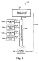
- FIG. 1 illustrates a simplified block diagram of a memory device 100 according to one embodiment of the present invention.
- Memory device 100 includes a write pulse generator 102, a distribution circuit 104, memory cells 106a, 106b, 106c, and 106d, and a sense circuit 108.
- memory cells 106a-106d are phase change memory cells that beneficially employ an amorphous to crystalline phase transition of memory material within the cell for storing data in the memory.
- Write pulse generator 102 is electrically coupled to distribution circuit 104 through signal path 110.
- Distribution circuit 104 is electrically coupled to memory cells 106a-106d through signal paths 112a-112d, respectively, and to sense circuit 108 through signal path 114.
- Write pulse generator 102 is electrically coupled to sense circuit 108 through a signal path 116.
- Each of the memory cells 106a-106d can be programmed into a memory state associated with a particular resistance value, and the resistance value is controlled using a suitable electrical write strategy.
- electrically coupled is not meant to mean that the elements must be directly coupled together, and intervening elements may be provided between the “electrically coupled” elements.
- each phase change memory cell 106a-106d includes phase change material providing a data storage location.
- the active region for the phase change memory cell is where the phase change material transitions between the crystalline state and the amorphous state for storing one bit, 1.5 bits, two bits, or several bits of data.
- write pulse generator 102 generates current or voltage pulses that are controllably directed to memory cells 106a-106d via distribution circuit 104.
- distribution circuit 104 includes a plurality of transistors that controllably direct current or voltage pulses to the memory cells.
- memory cells 106a-106d include a phase change material that can be changed from an amorphous state to a crystalline state, or from a crystalline state to an amorphous state, under influence of a temperature change. These crystalline memory states are useful for storing data in memory device 100.
- the memory state(s) can be assigned to the bit values, such as bit values "0" and "1.”
- the bit states of memory cells 106a-106d differ significantly in their electrical resistivity. In the amorphous state, a phase change material exhibits significantly higher resistivity than in the crystalline state. In this manner, sense amplifier 108 reads the cell resistance such that the bit value assigned to a particular memory cell 106a-106d is determined.
- write pulse generator 102 To program one of the memory cells 106a-106d within memory device 100, write pulse generator 102 generates a current or voltage pulse for heating the phase change material in the target memory cell. In one embodiment, write pulse generator 102 generates an appropriate current or voltage pulse, which is fed into distribution circuit 104 and distributed to the appropriate target memory cell 106a-106d. The current or voltage pulse amplitude and duration is controlled depending on whether the memory cell is being set or reset. Generally, a "set” operation of a memory cell heats the phase change material of the target memory cell above its crystallization temperature (but below its melting temperature) long enough to achieve the crystalline state. Generally, a “reset” operation of a memory cell heats the phase change material of the target memory cell above its melting temperature, and then quickly quenches/cools the material, thereby achieving the amorphous state.
- aspects of the present invention provide a memory cell stack including multiple layers of, for example, phase change materials having a variation in etch rates.
- a selective control of a thickness of each layer in the stack, in combination with the variation in the etch rate between the layers in the stack, enable a precise control of the geometry, size, and shape of the stack by controlled undercut etching of portions of the stack.
- Controlled undercut etching of different phase change materials within the stack provide memory cells having a suitably narrow current path through the stack that draw less power in changing memory states in the memory cells, which enables the use of smaller selection devices, and thus reduces an overall size for memory devices.
- Figures 2-11 illustrate various embodiments of a low power memory cell having an active region that locates large memory changing temperature gradients away from the opposing electrodes to provide improved memory cell lifetime and endurance.
- a stack of phase change material is provided between opposing electrodes that defines an active region width that is less than a width of either of a first phase change material and a second phase change material of the stack.
- the resulting phase change memory cells draw less power in changing memory states in the memory cells, which enables the use of smaller selection devices, and thus reduces an overall size for memory devices.
- the low power phase change memory cells generally include memory elements that have been fabricated by a controlled undercut etching of different phase change materials within the memory element.
- FIG. 2 illustrates a cross-sectional view of a memory cell 106 according to one embodiment of the present invention.
- memory cell 106 includes a first electrode 120, an opposing second electrode 122, and a stack 124 of phase change materials extending between first electrode 120 and second electrode 122.
- an additional conducting layer (not shown, but see, for example, layer 220 in Figure 11 ) is provided between first electrode 120 and stack 124.
- the interface formed between the additional conducting layer and stack 124 is, in one embodiment, an in-situ interface.
- stack 124 of phase change materials includes a first insulating layer 126 contacting first electrode 120, a second thermally insulating layer 128 contacting second electrode 122, and a phase change material 130 between first insulating layer 126 and second insulating layer 128, where layers 126, 128 can include phase change material and phase change material 130 is selected to have a higher electrical resistivity than either of layers 126, 128.
- layers 126, 128 include phase change materials such that stack 124 of phase change materials includes a first phase change material 126 contacting first electrode 120, a second phase change material 128 contacting second electrode 122, and a third phase change material 130 between first phase change material 126 and second phase change material 128.
- stack 124 includes a continuous gradient of phase change materials, as best illustrated in Figure 14 .
- Isolation material 132 surrounds stack 124 of phase change material and second electrode 122.
- isolation material 132 is an insulation dielectric and includes, for example, silicon dioxide (SiO 2 ), a porous oxide insulator, a low-k insulation material, or other suitable insulation materials.
- a plug landing pad 134 is subsequently coupled to memory cell 106 to enable electrical connectivity of memory cell 106 to distribution circuit 104 ( Figure 1 ), for example.
- plug landing pad 134 is a metal pad that includes titanium nitride (TiN), tungsten (W), tantalum nitride (TaN), a copper pad, or a pad of other suitable electrode material.
- memory cell 106 is fabricated directly onto an electrode plug 120 provided as a component of a pre-processed wafer 136, as best illustrated in Figures 3A and 3B.
- pre-processed wafer 136 includes electrode plug 120 disposed within a dielectric field 138.
- stack 124 of phase change material has an active region 140 that has a width D3 that is less than either a width D 1 of first phase change material 126 or a width D2 of second phase change material 128.
- third phase change material 130 has an active region width D3 that is less than either a width D1 of first phase change material 126 or a width D2 of second phase change material 128.
- Active region 140 provides a reduced power/current consumption for memory cell 106.
- Active region 140 has width D3 that is less than widths D 1 and D2, such that the largest temperature gradient within cell 106 will occur in active region 140.
- active region 140 locates this region of largest temperature gradient within cell 106 away from electrodes 120, 122, resulting in improved memory lifetime and endurance.
- width D3 is less than width D1, and width D1 is less than width D2. In another embodiment, width D3 is less than width D2, and width D2 is less than width D1. In general, widths D 1 and D2 are between about 10-100 nm, and width D3 is less than widths D1 and D2, where width D3 is between about 5-50 nm.
- First electrode 120 and second electrode 122 include titanium nitride (TiN), tantalum nitride (TaN), tungsten (W), or other suitable electrode material.
- electrode plug 120 is a TiN plug, a tungsten plug, a copper plug, or a plug of other suitable electrode material.
- plugs 120, 122 include a stack of different materials, such as a stack that includes TiN disposed on W.
- each of phase change materials 126, 128, and 130 includes chalcogenide alloys having one or more elements from Group VI of the periodic table, such as Tellurium and/or Selenium and/or Sulfur, and their alloys. In one embodiment, at least one of phase change materials 126, 128, and 130 includes chalcogenide alloys having one or more elements from Group VI of the periodic table, such as Tellurium and/or Selenium and/or Sulfur, and their alloys.
- phase change materials 126, 128, and 130 is chalcogen-free, i.e., is a phase change material that does not contain Tellurium, Selenium, or Sulfur, or alloys of Tellurium, Selenium, or Sulfur.
- Suitable materials for stack 124 of phase change material include, for example, compounds of GeSbTe, SbTe, GeTe, AgInSbTe, GeSb, GaSb, InSb, GeGaInSb.
- stack 124 includes one or more of the elements Ge, Sb, Te, Ga, As, In, Se, and S. In another embodiment, stack 124 includes a continuous gradient of the above-identified phase change materials. In addition, one or more of phase change materials 126, 128, and 130 may be selectively doped with nitrogen, oxygen, silicon, or other suitable materials.
- Stack 124 of phase change material includes third phase change material 130 disposed between first phase change material 126 and second phase change material 128.
- third phase change material 130 has an etch rate relative to a reactive etch chemistry that is greater than an etch rate of either first phase change material 126 or second change material 128 relative to the same reactive etch chemistry.
- third phase change material 130 has an etch rate of between about 5 nm/h and about 30 nm/h for a given etchant.
- the given etchant has an alkaline pH of about 11
- the third phase change material 130 has an etch rate of about 20 nm/h
- first phase change material 126 and second change material 128 have an etch rate of less than 5 nm/h. Consequently, during etching by the given etchant, third phase change material 130 is etched to a greater extent than first phase change material 126 or second phase change material 128. In this manner, third phase change material 130 is reduced to a width D3 that is less than a width D1 of first phase change material 126, or a width D2 of second phase change material 128.
- first phase change material 126 is different from second phase change material 128, and second phase change material 128 is different from third phase change material 130. In another embodiment, first phase change material 126 is substantially the same as second phase change material 128, and third phase change material 130 is different than first phase change material 126.
- third phase change material 130 has an electrical resistivity that is greater than an electrical resistivity of first phase change material 126 and an electrical resistivity of second phase change material 128.
- phase change materials have greater etch rates than amorphous phase change materials.
- third phase change material 130 that otherwise defines active region 140, have a crystallization temperature that is different than a crystallization temperature of first phase change material 126 and a crystallization temperature of second phase change material 128.
- third phase change material 130 has a lower crystallization temperature than first phase change material 126 and second phase change material 128, such that during an annealing process, third phase change material 130 is annealed to define an increased level of crystallization. In this manner, when annealed, third phase change material 130 will have an etch rate that is greater than an etch rate for first and second phase change materials 126, 128.
- Figures 3-10 illustrate various embodiments related to the fabrication of a low power memory cell having an active region that locates large memory changing temperature gradients away from the opposing electrodes to provide improved memory cell lifetime and endurance.
- a stack of material including multiple layers of, for example, phase change materials having a variation in etch rates.
- a selective control of a thickness of each layer in the stack, in combination with the variation in the etch rate between the layers in the stack, enable a precise control of the geometry, size, and shape of the stack by controlled undercut etching of portions of the stack.
- Controlled undercut etching of different phase change materials within the stack provide memory cells having a suitably narrow current path through the stack that draw less power in changing memory states in the memory cells, which enables the use of smaller selection devices, and thus reduces an overall size for memory devices.
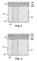
- Figure 3 illustrates a cross-sectional view of a stack 144 of phase change materials disposed on pre-processed wafer 136 according to one embodiment of the present invention.
- Stack 144 includes a first layer 126a of phase change material in contact with first electrode 120, a second layer 128a of phase change material, and a third layer 130a of phase change material extending between first layer 126a of phase change material and second layer 128a of phase change material.
- first layer 126a of phase change material is deposited using chemical vapor deposition (CVD), atomic layer deposition (ALD), metal organic chemical vapor deposition (MOCVD), plasma vapor deposition (PVD), jet vapor deposition (JVD), or other suitable depositions techniques.
- CVD chemical vapor deposition
- ALD atomic layer deposition
- MOCVD metal organic chemical vapor deposition
- PVD plasma vapor deposition
- JVD jet vapor deposition
- third layer 130a of phase change material is deposited onto first layer 126a of phase change material using a deposition technique of CVD, ALD, MOCVD, PVD, JVD, or other suitable deposition techniques.
- second layer 128a of phase change material is deposited onto third layer 130a of phase change material using a deposition technique of CVD, ALD, MOCVD, PVD, JVD, or other suitable deposition techniques.
- Figure 4 illustrates a cross-sectional view of an electrode layer 122a deposited onto stack 144 of phase change materials according to one embodiment of the present invention.
- electrode layer 122a is deposited onto second layer 128a of phase change material using a deposition technique of CVD, ALD, MOCVD, PVD, JVD, or other suitable deposition techniques.
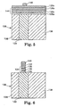
- Figure 5 illustrates a cross-sectional view of a mask layer 148 deposited onto an electrode layer 122a according to one embodiment of the present invention.
- mask layer 148 is a photoresist/arc combination that is coated onto electrode layer 122a. Photoresist/arc combination is stripped after a pillar dry etch, for example, or stripped after a pullback etch.
- mask layer 148 is a hardmask deposited onto electrode layer 122a and includes a silicon nitride, for example, deposited by a suitable deposition technique, such as CVD, ALD, MOCVD, PVD, and/or JVD.
- mask layer 148 is a stop etch layer including silicon nitride, such as SiN, or SiON, or other suitable stop etch materials.
- hard mask layer 148 can be removed, or planarized, in a suitable mechanical process, such as a chemical mechanical polish/planarization process without prior stripping processes.
- mask layer 148 is selected to define a width of one of or both first phase change material 126 and second phase change material 128 ( Figure 2 ).
- Figure 6 illustrates a cross-sectional view after a dry etch of stack 144 of phase change materials ( Figure 5 ) according to one embodiment of the present invention.
- a dry etch of electrode layer 122a and stack 144 ( Figure 5 ) is initiated to define a pillar having a stack 124 of phase change materials.
- Stack 124 of phase change materials includes first 126, second 128, and third 130 phase change materials each having an approximately equal width defined by a width of mask layer 148.
- stack 124 of phase change materials is annealed to selectively crystallize one or more of the phase change materials 126, 128, and 130.
- third phase change material 130 is selected to have a lower crystallization temperature than first phase change material 126 and second phase change material 128, such that after annealing, third phase change material 130 has an increased level of crystallization.
- the selective increase in the crystallization of third phase change material 130 predisposes third phase change material 130 to have an etch rate relative to a reactive etch chemistry that is greater than an etch rate of either of the first phase change material 126 and the second phase change material 128 relative to the same reactive etch chemistry.
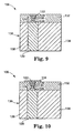
- Figure 7 illustrates a cross-sectional view of stack 124 after an undercut etch according to one embodiment of the present invention.
- the undercut etch is a wet chemical pull-back etch that pull-back etches hard mask layer 148 ( Figure 6 ) and undercut etches third phase change material 130.
- the undercut etch illustrated in Figure 7 is completed in the gas phase in a vapor etch reactor, or alternatively, the undercut etch is a plasma dry etch.
- the third phase change material 130 is selected to have an etch rate relative to the etch chemistry employed that is greater than an etch rate of either the first phase change material 126 or the second phase change material 128 relative to the same etch chemistry. In this manner, width D3 of the third phase change material 130 is less than width D2 of second phase change material 128 after the undercut etch is completed.
- Figure 8 illustrates a cross-sectional view of an isolation material 132 deposited around stack 124 to isolate memory cell 106 according to one embodiment of the present invention.
- isolation material 132 is a low-k isolation material. Suitable isolation materials include silicon dioxide, silicon nitride, porous oxide, or other suitable oxide isolation materials.
- isolation material 132 is deposited by a high density plasma chemical vapor deposition (HDP CVD) process. In one embodiment, a radio frequency biased HDP CVD process is employed to deposit a silicon dioxide isolation material 132 along a high aspect feature, such as stack 124.
- HDP CVD high density plasma chemical vapor deposition
- Figure 9 illustrates a memory cell 106 including a planarized isolation layer 132 according to one embodiment of the present invention.
- isolation layer 132 is planarized in a chemical mechanical polishing (CMP) process, although other suitable planarization processes are acceptable.
- CMP chemical mechanical polishing
- the CMP process stops within top electrode 122 where the CMP process includes a selectivity against the top electrode metallization.
- Plug landing pad 134 includes a blanket metal deposition of, for example, titanium nitride (TiN), followed by lithographic and etch processes.
- plug landing pad 134 includes a metallization of Al/Cu using a dual damascene process.
- plug landing pad 134 is a tungsten pad deposited in a plug formation process.
- FIGS 2-10 illustrate exemplary embodiments suited for fabrication of memory cell 106.
- Memory cell 106 includes first electrode 120, an opposing second electrode 122, and stack 124 of phase change material extending between first electrode 120 and second electrode 122.
- Plug landing pad 134 is provided to enable electrical connectivity of memory cell 106 to distribution circuit 104 ( Figure 1 ).
- a width D3 of third phase change material 130 is narrower than other layers of stack 124 and defines an active region 140 ( Figure 2 ), and memory cell 106 is a low power cell that locates large memory changing temperature gradients away from electrodes 120, 122 to provide memory cell 106 with improved lifetime and endurance.
- Figure 11 illustrates another embodiment of a low power memory cell having an active region that locates large memory changing temperature gradients away from the opposing electrodes to provide improved memory cell lifetime and endurance.
- a stack of phase change material is provided between opposing electrodes that defines an active region width that is less than a width of either of a first phase change material and a second phase change material of the stack.
- Figure 11 illustrates a cross-sectional view of a memory cell 206 according to another embodiment of the present invention.
- memory cell 206 is fabricated onto plug 120 provided in a pre-processed wafer 136 and includes a dedicated electrode 220 in contact with plug 120.
- Memory cell 206 includes first electrode 220, an opposing second electrode 222, and a stack 224 of phase change materials extending between first electrode 220 and second electrode 222.
- stack 224 of phase change materials includes a first phase change material 226 contacting first electrode 220, a second phase change material 228 contacting second electrode 222, and a third phase change material 230 between first phase change material 226 and second phase change material 228.
- stack 224 includes a continuous gradient of phase change materials, as best illustrated in Figure 14 .
- Isolation material 232 surrounds stack 224 of phase change material and electrodes 220, 222.
- isolation material 232 is an insulation dielectric and includes, for example, silicon dioxide (SiO 2 ) a porous oxide insulator, a low-k insulation material, or other suitable insulation materials.
- SiO 2 silicon dioxide
- a pad and other upper layers (not shown), in addition to lower layers (not shown), are subsequently coupled to memory cell 206 to enable electrical connectivity of memory cell 206 to distribution circuit 104 ( Figure 1 ), for example.
- first phase change material 226 is different from second phase change material 228, and second phase change material 228 is different from third phase change material 230.
- first phase change material 226 is substantially the same as second phase change material 228, and third phase change material 230 is different than first phase change material 226.
- Figures 12-14 illustrate other embodiments of a low power memory cell having an active region that locates large memory changing temperature gradients away from the opposing electrodes to provide improved memory cell lifetime and endurance.
- a stack of phase change material is provided between opposing electrodes that has an active region width that is less than a width of either of a first phase change material and a second phase change material of the stack.
- Figure 12 illustrates a cross-sectional view of a stack 324 of phase change materials in a memory cell 306 according to another embodiment of the present invention.
- Memory cell 306 includes first electrode 320, an opposing second electrode 322, and a stack 324 of phase change materials extending between first electrode 320 and second electrode 322.
- stack 324 of phase change materials includes a first phase change material 326 contacting first electrode 320, a second phase change material 328 contacting second electrode 322, and a third phase change material 330 between first phase change material 326 and second phase change material 328.
- Isolation material 332 surrounds stack 324 of phase change material and electrodes 320, 322.
- first phase change material 326 is different from second phase change material 328, and second phase change material 328 is different from third phase change material 330, although other suitable combinations are acceptable.
- first phase change material 326 and third phase change material 330 each have an etch rate relative to a reactive etch chemistry that is greater than an etch rate of second phase change material 328 relative to the same reactive etch chemistry.
- a width D1 of first phase change material 326 and a width D3 of third phase change material 330 are each less than a width D2 of second phase change material 328. Since width D3 of third phase change material 330 is the narrowest width within stack 324, less power is consumed in changing a memory state in memory cell 306, and large memory changing temperature gradients are located away from the opposing electrodes 320, 322.
- Figure 13 illustrates a cross-sectional view of a stack 424 of phase change materials in a memory cell 406 according to another embodiment of the present invention.
- Memory cell 406 includes first electrode 420, an opposing second electrode 422, and a stack 424 of phase change materials extending between first electrode 420 and second electrode 422.
- stack 424 of phase change materials includes a first phase change material 426 contacting first electrode 420, a second phase change material 428 contacting second electrode 422, and a third phase change material 430 between first phase change material 426 and second phase change material 428.
- Isolation material 432 surrounds stack 424 of phase change material and electrodes 420, 422.
- first phase change material 426 is different from second phase change material 428, and second phase change material 428 is different from third phase change material 430, although other suitable combinations are acceptable.
- second phase change material 428 and third phase change material 430 each an etch rate relative to a reactive etch chemistry that is greater than an etch rate of first phase change material 426 relative to the same reactive etch chemistry.
- a width D2 of second phase change material 428 and a width D3 of third phase change material 430 are each less than a width D1 of first phase change material 426. Since width D3 of third phase change material 430 is the narrowest width within stack 424, less power is consumed in changing a memory state in memory cell 406, and large memory changing temperature gradients are located away from the opposing electrodes 420, 422.
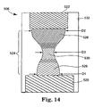
- Figure 14 illustrates a cross-sectional view of a gradient 524 of phase change materials in a memory cell 506 according to one embodiment of the present invention.
- Memory cell 506 includes first electrode 520, an opposing second electrode 522, and a stack 524 of phase change materials extending between first electrode 520 and second electrode 522.
- stack 524 of phase change materials includes a first phase change material 526 contacting first electrode 520, a second phase change material 528 contacting second electrode 522, and a third phase change material 530 between first phase change material 526 and second phase change material 528.
- Isolation material 532 surrounds stack 524 of phase change material and electrodes 520, 522.
- stack 524 of phase change materials defines a continuous pillar of phase change material that itself has a gradient of electrical and material properties.
- a central portion of stack 524 includes third phase change material 530, and it is desired that third phase change material 530 be selected and deposited to have an etch rate relative to a reactive etch chemistry that is greater than an etch rate of either of first phase change material 526 and second phase change material 528 relative to the same reactive etch chemistry.
- third phase change material 530 has an electrical resistivity that is greater than an electrical resistivity of either of first phase change material 526 and second phase change material 528.
- first phase change material 526 and third phase change material 530 each have an etch rate relative to a reactive etch chemistry that is greater than an etch rate of second phase change material 528 relative to the same reactive etch chemistry.
- a width D 1 of first phase change material 526 and a width D3 of third phase change material 530 are each less than a width D2 of second phase change material 528. Since width D3 of third phase change material 530 is the narrowest width within stack 524, less power is consumed in changing a memory state in memory cell 506, and large memory changing temperature gradients are located away from the opposing electrodes 520, 522.
- a low power memory cell having an active region that locates large memory changing temperature gradients away from the opposing electrodes to provide improved memory cell lifetime and endurance.
- a stack of phase change material is provided between opposing electrodes that has an active region width that is less than a width of either of a first phase change material and a second phase change material of the stack.
- the phase change memory cells including the stack of phase change material draw less power in changing memory states in the memory cells, which enables the use of smaller selection devices, and thus reduces an overall size for memory devices.
- the low power phase change memory cells include memory elements that have been fabricated by a controlled undercut etching of different phase change materials within the memory element.
Description
- Semiconductor memories provide memory storage for electronic devices and have become very popular in the electronic products industry. In general, many semiconductor chips are typically fabricated (or built) on a silicon wafer. The semiconductor chips are individually separated from the wafer for subsequent use as memory in electronic devices. In this regard, the semiconductor chips contain an array of memory cells that are configured to store retrievable data, often characterized by the logic values of 0 and 1.
- One class of semiconductor memories is resistive memories. They typically use two or more different resistive values of a switchable resistor to define cell states in the memory useful in storing data. One particular type of resistive memory is a phase change memory. In one known structure of a phase change memory cell, the memory cell is formed at the intersection of a phase change memory material and an electrode. Passing energy of an appropriate value through the electrode heats the phase change memory cell, thus affecting a phase/state change in its atomic structure. The phase change memory cell can be selectively switched between logic states 0 and 1, for example, and/or selectively switched between multiple logic states.
- Materials that exhibit the above-noted phase change memory characteristics include elements of Group VI of the periodic table (such as Tellurium and Selenium) and their alloys, referred to as chalcogenides or chalcogenic materials. Other non-chalcogenide materials also exhibit phase change memory characteristics.
- The atomic structure of one type of phase change memory cell can be switched between an amorphous state and one or more crystalline states. The amorphous state has greater electrical resistance than the crystalline state(s), and typically includes a disordered atomic structure with only short range coordination. In contrast, the crystalline states each generally have a more ordered atomic structure, and lower electrical resistance (and higher electrical conductivity).
- The atomic structure of a phase change material becomes more ordered when maintained at (or slightly above) the crystallization temperature. A subsequent slow cooling of the material results in a stable orientation of the atomic structure in the highly ordered (crystalline) state. To switch back, or reset to the amorphous state, for example in the chalcogenide material, the local temperature is generally raised above the melting temperature (approximately 600 degrees Celsius) to achieve a highly random atomic structure, and then rapidly cooled to "lock" the atomic structure in the amorphous state.
- The temperature-induced set/rest changes in the memory cell(s) create locally elevated temperatures, or hot spots, within each cell. Hot spots in memory cells require an increase in current (and thus power) to reset a memory state in the memory cell. It is desired to reduce the power needed to change memory states in memory cells to enable the use of smaller selection devices, thus reducing an overall size for memory devices, in general.
- In "Phase change random access memory, thermal analysis" by Sadeghipour et al. (pages 660 - 665, XP010923735 from 10th Intersociety Conference on Thermal and Thermomechanical Phenomena in Electronics Systems, 30 May - 2 June 2006, San Diego, Ca. USA) several problems in the field of phase change random access memories, such as reliability (lifetime), power consumption and speed, and thermal issues are discussed. In light of thermal engineering, different memory cell structures are described.
- In
KR 20060079455 A - Non pre-published
EP 1 783 844 A2 describes a phase change memory cell with a first electrode, a second electrode and a first portion of phase-change material contacting the first electrode. The memory cell includes a second portion of phase-change material contacting the second electrode and a third portion of phase-change material between the first portion and the second portion, wherein a phase-change material composition of the third portion and the second portion gradually transitions from the third portion to the second portion. - Non pre-published
EP 1 724 850 A2 describes a phase change memory cell with a first electrode, a second electrode, and phase-change material including a first portion contacting the first electrode, a second portion contacting the second electrode, and a third portion between the first portion and the second portion. A width of the third portion is less than a width of the first portion and a width of the second portion. - For these and other reasons, there is a need for the present invention.
- The present invention provides a memory cell that includes a first electrode and an opposing second electrode, and a memory stack between the first and second electrodes. The memory stack includes a first layer of thermal isolation material contacting the first electrode, a second layer of thermal isolation material contacting the second electrode, and a phase change material between the first layer of thermal isolation material and the second layer of thermal isolation material. In this regard, the phase change material has an active region width that is less than a width of either of the first layer of thermal isolation material and the second layer of thermal isolation material. The phase change material has an etch rate at a given reactive etch chemistry that is greater than an etch rate of either of the first and second layers of thermal insulation material at the given reactive etch chemistry.
- The present invention also provides a method of fabricating such memory cell and a memory device comprising an array of such cells.
- The accompanying drawings are included to provide a further understanding of the present invention and are incorporated in and constitute a part of this specification. The drawings illustrate the embodiments of the present invention and together with the description serve to explain the principles of the invention. Other embodiments of the present invention and many of the intended advantages of the present invention will be readily appreciated as they become better understood by reference to the following detailed description. The elements of the drawings are not necessarily to scale relative to each other. Like reference numerals designate corresponding similar parts.
-
Figure 1 illustrates a simplified block diagram of a memory device including memory cells according to one embodiment of the present invention. -
Figure 2 illustrates a cross-sectional view of a memory cell according to one embodiment of the present invention. -
Figure 3 illustrates a cross-sectional view of a stack of phase change materials disposed on a pre-processed wafer according to one embodiment of the present invention. -
Figure 4 illustrates a cross-sectional view of an electrode layer deposited onto a stack of phase change materials according to one embodiment of the present invention. -
Figure 5 illustrates a cross-sectional view of a resist and a mask deposited onto an electrode layer of a memory cell according to one embodiment of the present invention. -
Figure 6 illustrates a cross-sectional view of a stack of phase change materials after a dry etch according to one embodiment of the present invention. -
Figure 7 illustrates a cross-sectional view of a stack of phase change materials after a wet pull-back etch according to one embodiment of the present invention. -
Figure 8 illustrates a cross-sectional view of an isolation material surrounding a stack of phase change materials according to one embodiment of the present invention. -
Figure 9 illustrates a planarized isolation material of a memory cell according to one embodiment of the present invention. -
Figure 10 illustrates a cross-sectional view of memory cell having a stack of phase change materials and a plug landing pad according to one embodiment of the present invention. -
Figure 11 illustrates a cross-sectional view of a memory cell according to another embodiment of the present invention. -
Figure 12 illustrates a cross-sectional view of a stack of phase change materials in a memory cell according to another embodiment of the present invention. -
Figure 13 illustrates a cross-sectional view of a stack of phase change materials in a memory cell according to another embodiment of the present invention. -
Figure 14 illustrates a cross-sectional view of a gradient of phase change materials in a memory cell according to one embodiment of the present invention. -
Figure 1 illustrates a simplified block diagram of amemory device 100 according to one embodiment of the present invention.Memory device 100 includes awrite pulse generator 102, adistribution circuit 104,memory cells sense circuit 108. In one embodiment,memory cells 106a-106d are phase change memory cells that beneficially employ an amorphous to crystalline phase transition of memory material within the cell for storing data in the memory.Write pulse generator 102 is electrically coupled todistribution circuit 104 throughsignal path 110.Distribution circuit 104 is electrically coupled tomemory cells 106a-106d throughsignal paths 112a-112d, respectively, and to sensecircuit 108 throughsignal path 114.Write pulse generator 102 is electrically coupled to sensecircuit 108 through asignal path 116. Each of thememory cells 106a-106d can be programmed into a memory state associated with a particular resistance value, and the resistance value is controlled using a suitable electrical write strategy. - As used herein the term "electrically coupled" is not meant to mean that the elements must be directly coupled together, and intervening elements may be provided between the "electrically coupled" elements.
- In one embodiment, each phase
change memory cell 106a-106d includes phase change material providing a data storage location. The active region for the phase change memory cell is where the phase change material transitions between the crystalline state and the amorphous state for storing one bit, 1.5 bits, two bits, or several bits of data. - In one embodiment, write
pulse generator 102 generates current or voltage pulses that are controllably directed tomemory cells 106a-106d viadistribution circuit 104. In one embodiment,distribution circuit 104 includes a plurality of transistors that controllably direct current or voltage pulses to the memory cells. - In one embodiment,
memory cells 106a-106d include a phase change material that can be changed from an amorphous state to a crystalline state, or from a crystalline state to an amorphous state, under influence of a temperature change. These crystalline memory states are useful for storing data inmemory device 100. The memory state(s) can be assigned to the bit values, such as bit values "0" and "1." The bit states ofmemory cells 106a-106d differ significantly in their electrical resistivity. In the amorphous state, a phase change material exhibits significantly higher resistivity than in the crystalline state. In this manner,sense amplifier 108 reads the cell resistance such that the bit value assigned to aparticular memory cell 106a-106d is determined. - To program one of the
memory cells 106a-106d withinmemory device 100, writepulse generator 102 generates a current or voltage pulse for heating the phase change material in the target memory cell. In one embodiment, writepulse generator 102 generates an appropriate current or voltage pulse, which is fed intodistribution circuit 104 and distributed to the appropriatetarget memory cell 106a-106d. The current or voltage pulse amplitude and duration is controlled depending on whether the memory cell is being set or reset. Generally, a "set" operation of a memory cell heats the phase change material of the target memory cell above its crystallization temperature (but below its melting temperature) long enough to achieve the crystalline state. Generally, a "reset" operation of a memory cell heats the phase change material of the target memory cell above its melting temperature, and then quickly quenches/cools the material, thereby achieving the amorphous state. - Aspects of the present invention provide a memory cell stack including multiple layers of, for example, phase change materials having a variation in etch rates. A selective control of a thickness of each layer in the stack, in combination with the variation in the etch rate between the layers in the stack, enable a precise control of the geometry, size, and shape of the stack by controlled undercut etching of portions of the stack. Controlled undercut etching of different phase change materials within the stack provide memory cells having a suitably narrow current path through the stack that draw less power in changing memory states in the memory cells, which enables the use of smaller selection devices, and thus reduces an overall size for memory devices.
-
Figures 2-11 illustrate various embodiments of a low power memory cell having an active region that locates large memory changing temperature gradients away from the opposing electrodes to provide improved memory cell lifetime and endurance. In general, a stack of phase change material is provided between opposing electrodes that defines an active region width that is less than a width of either of a first phase change material and a second phase change material of the stack. The resulting phase change memory cells draw less power in changing memory states in the memory cells, which enables the use of smaller selection devices, and thus reduces an overall size for memory devices. The low power phase change memory cells generally include memory elements that have been fabricated by a controlled undercut etching of different phase change materials within the memory element. -
Figure 2 illustrates a cross-sectional view of amemory cell 106 according to one embodiment of the present invention. In one embodiment,memory cell 106 includes afirst electrode 120, an opposingsecond electrode 122, and astack 124 of phase change materials extending betweenfirst electrode 120 andsecond electrode 122. In one embodiment, an additional conducting layer (not shown, but see, for example,layer 220 inFigure 11 ) is provided betweenfirst electrode 120 andstack 124. The interface formed between the additional conducting layer and stack 124 is, in one embodiment, an in-situ interface. - In one embodiment, stack 124 of phase change materials includes a first insulating
layer 126 contactingfirst electrode 120, a second thermally insulatinglayer 128 contactingsecond electrode 122, and aphase change material 130 between first insulatinglayer 126 and second insulatinglayer 128, wherelayers phase change material 130 is selected to have a higher electrical resistivity than either oflayers stack 124 of phase change materials includes a firstphase change material 126 contactingfirst electrode 120, a secondphase change material 128 contactingsecond electrode 122, and a thirdphase change material 130 between firstphase change material 126 and secondphase change material 128. In another embodiment, stack 124 includes a continuous gradient of phase change materials, as best illustrated inFigure 14 . -
Isolation material 132 surroundsstack 124 of phase change material andsecond electrode 122. In one embodiment,isolation material 132 is an insulation dielectric and includes, for example, silicon dioxide (SiO2), a porous oxide insulator, a low-k insulation material, or other suitable insulation materials. - In one embodiment, a
plug landing pad 134 is subsequently coupled tomemory cell 106 to enable electrical connectivity ofmemory cell 106 to distribution circuit 104 (Figure 1 ), for example. In one embodiment, pluglanding pad 134 is a metal pad that includes titanium nitride (TiN), tungsten (W), tantalum nitride (TaN), a copper pad, or a pad of other suitable electrode material. In one embodiment,memory cell 106 is fabricated directly onto anelectrode plug 120 provided as a component of apre-processed wafer 136, as best illustrated inFigures 3A and 3B. In one embodiment,pre-processed wafer 136 includeselectrode plug 120 disposed within adielectric field 138. - In one embodiment, stack 124 of phase change material has an
active region 140 that has a width D3 that is less than either a width D 1 of firstphase change material 126 or a width D2 of secondphase change material 128. In particular, thirdphase change material 130 has an active region width D3 that is less than either a width D1 of firstphase change material 126 or a width D2 of secondphase change material 128. -
Active region 140 provides a reduced power/current consumption formemory cell 106.Active region 140 has width D3 that is less than widths D 1 and D2, such that the largest temperature gradient withincell 106 will occur inactive region 140. Thus,active region 140 locates this region of largest temperature gradient withincell 106 away fromelectrodes - In one embodiment, width D3 is less than width D1, and width D1 is less than width D2. In another embodiment, width D3 is less than width D2, and width D2 is less than width D1. In general, widths D 1 and D2 are between about 10-100 nm, and width D3 is less than widths D1 and D2, where width D3 is between about 5-50 nm.
-
First electrode 120 andsecond electrode 122 include titanium nitride (TiN), tantalum nitride (TaN), tungsten (W), or other suitable electrode material. In one embodiment,electrode plug 120 is a TiN plug, a tungsten plug, a copper plug, or a plug of other suitable electrode material. In one embodiment, plugs 120, 122 include a stack of different materials, such as a stack that includes TiN disposed on W. - In one embodiment, each of
phase change materials phase change materials phase change materials stack 124 of phase change material include, for example, compounds of GeSbTe, SbTe, GeTe, AgInSbTe, GeSb, GaSb, InSb, GeGaInSb. - In other embodiments,
stack 124 includes one or more of the elements Ge, Sb, Te, Ga, As, In, Se, and S. In another embodiment, stack 124 includes a continuous gradient of the above-identified phase change materials. In addition, one or more ofphase change materials -
Stack 124 of phase change material includes thirdphase change material 130 disposed between firstphase change material 126 and secondphase change material 128. In general, and as best illustrated inFigure 8 , thirdphase change material 130 has an etch rate relative to a reactive etch chemistry that is greater than an etch rate of either firstphase change material 126 orsecond change material 128 relative to the same reactive etch chemistry. - For example, in one embodiment third
phase change material 130 has an etch rate of between about 5 nm/h and about 30 nm/h for a given etchant. In one embodiment, the given etchant has an alkaline pH of about 11, and the thirdphase change material 130 has an etch rate of about 20 nm/h, and firstphase change material 126 andsecond change material 128 have an etch rate of less than 5 nm/h. Consequently, during etching by the given etchant, thirdphase change material 130 is etched to a greater extent than firstphase change material 126 or secondphase change material 128. In this manner, thirdphase change material 130 is reduced to a width D3 that is less than a width D1 of firstphase change material 126, or a width D2 of secondphase change material 128. - In one embodiment, first
phase change material 126 is different from secondphase change material 128, and secondphase change material 128 is different from thirdphase change material 130. In another embodiment, firstphase change material 126 is substantially the same as secondphase change material 128, and thirdphase change material 130 is different than firstphase change material 126. - In general, it is desired that third
phase change material 130 has an electrical resistivity that is greater than an electrical resistivity of firstphase change material 126 and an electrical resistivity of secondphase change material 128. - In general, crystalline phase change materials have greater etch rates than amorphous phase change materials. In this regard, it is desired that third
phase change material 130, that otherwise definesactive region 140, have a crystallization temperature that is different than a crystallization temperature of firstphase change material 126 and a crystallization temperature of secondphase change material 128. Preferably, thirdphase change material 130 has a lower crystallization temperature than firstphase change material 126 and secondphase change material 128, such that during an annealing process, thirdphase change material 130 is annealed to define an increased level of crystallization. In this manner, when annealed, thirdphase change material 130 will have an etch rate that is greater than an etch rate for first and secondphase change materials -
Figures 3-10 illustrate various embodiments related to the fabrication of a low power memory cell having an active region that locates large memory changing temperature gradients away from the opposing electrodes to provide improved memory cell lifetime and endurance. In general, a stack of material is provided including multiple layers of, for example, phase change materials having a variation in etch rates. A selective control of a thickness of each layer in the stack, in combination with the variation in the etch rate between the layers in the stack, enable a precise control of the geometry, size, and shape of the stack by controlled undercut etching of portions of the stack. Controlled undercut etching of different phase change materials within the stack provide memory cells having a suitably narrow current path through the stack that draw less power in changing memory states in the memory cells, which enables the use of smaller selection devices, and thus reduces an overall size for memory devices. -
Figure 3 illustrates a cross-sectional view of astack 144 of phase change materials disposed onpre-processed wafer 136 according to one embodiment of the present invention.Stack 144 includes afirst layer 126a of phase change material in contact withfirst electrode 120, asecond layer 128a of phase change material, and athird layer 130a of phase change material extending betweenfirst layer 126a of phase change material andsecond layer 128a of phase change material. - In one embodiment,
first layer 126a of phase change material is deposited using chemical vapor deposition (CVD), atomic layer deposition (ALD), metal organic chemical vapor deposition (MOCVD), plasma vapor deposition (PVD), jet vapor deposition (JVD), or other suitable depositions techniques. - In one embodiment,
third layer 130a of phase change material is deposited ontofirst layer 126a of phase change material using a deposition technique of CVD, ALD, MOCVD, PVD, JVD, or other suitable deposition techniques. - In one embodiment,
second layer 128a of phase change material is deposited ontothird layer 130a of phase change material using a deposition technique of CVD, ALD, MOCVD, PVD, JVD, or other suitable deposition techniques. -
Figure 4 illustrates a cross-sectional view of anelectrode layer 122a deposited ontostack 144 of phase change materials according to one embodiment of the present invention. In one embodiment,electrode layer 122a is deposited ontosecond layer 128a of phase change material using a deposition technique of CVD, ALD, MOCVD, PVD, JVD, or other suitable deposition techniques. -
Figure 5 illustrates a cross-sectional view of amask layer 148 deposited onto anelectrode layer 122a according to one embodiment of the present invention. In one embodiment,mask layer 148 is a photoresist/arc combination that is coated ontoelectrode layer 122a. Photoresist/arc combination is stripped after a pillar dry etch, for example, or stripped after a pullback etch. - In another embodiment,
mask layer 148 is a hardmask deposited ontoelectrode layer 122a and includes a silicon nitride, for example, deposited by a suitable deposition technique, such as CVD, ALD, MOCVD, PVD, and/or JVD. In one embodiment,mask layer 148 is a stop etch layer including silicon nitride, such as SiN, or SiON, or other suitable stop etch materials. In this regard,hard mask layer 148 can be removed, or planarized, in a suitable mechanical process, such as a chemical mechanical polish/planarization process without prior stripping processes. In one embodiment,mask layer 148 is selected to define a width of one of or both firstphase change material 126 and second phase change material 128 (Figure 2 ). -
Figure 6 illustrates a cross-sectional view after a dry etch ofstack 144 of phase change materials (Figure 5 ) according to one embodiment of the present invention. In one embodiment, a dry etch ofelectrode layer 122a and stack 144 (Figure 5 ) is initiated to define a pillar having astack 124 of phase change materials.Stack 124 of phase change materials includes first 126, second 128, and third 130 phase change materials each having an approximately equal width defined by a width ofmask layer 148. - In one embodiment, stack 124 of phase change materials is annealed to selectively crystallize one or more of the
phase change materials phase change material 130 is selected to have a lower crystallization temperature than firstphase change material 126 and secondphase change material 128, such that after annealing, thirdphase change material 130 has an increased level of crystallization. The selective increase in the crystallization of thirdphase change material 130 predisposes thirdphase change material 130 to have an etch rate relative to a reactive etch chemistry that is greater than an etch rate of either of the firstphase change material 126 and the secondphase change material 128 relative to the same reactive etch chemistry. -
Figure 7 illustrates a cross-sectional view ofstack 124 after an undercut etch according to one embodiment of the present invention. In one embodiment, the undercut etch is a wet chemical pull-back etch that pull-back etches hard mask layer 148 (Figure 6 ) and undercut etches thirdphase change material 130. In one embodiment, the undercut etch illustrated inFigure 7 is completed in the gas phase in a vapor etch reactor, or alternatively, the undercut etch is a plasma dry etch. In any regard, the thirdphase change material 130 is selected to have an etch rate relative to the etch chemistry employed that is greater than an etch rate of either the firstphase change material 126 or the secondphase change material 128 relative to the same etch chemistry. In this manner, width D3 of the thirdphase change material 130 is less than width D2 of secondphase change material 128 after the undercut etch is completed. -
Figure 8 illustrates a cross-sectional view of anisolation material 132 deposited aroundstack 124 to isolatememory cell 106 according to one embodiment of the present invention. In one embodiment,isolation material 132 is a low-k isolation material. Suitable isolation materials include silicon dioxide, silicon nitride, porous oxide, or other suitable oxide isolation materials. In one embodiment,isolation material 132 is deposited by a high density plasma chemical vapor deposition (HDP CVD) process. In one embodiment, a radio frequency biased HDP CVD process is employed to deposit a silicondioxide isolation material 132 along a high aspect feature, such asstack 124. -
Figure 9 illustrates amemory cell 106 including aplanarized isolation layer 132 according to one embodiment of the present invention. In one embodiment,isolation layer 132 is planarized in a chemical mechanical polishing (CMP) process, although other suitable planarization processes are acceptable. In one embodiment, the CMP process stops withintop electrode 122 where the CMP process includes a selectivity against the top electrode metallization. -
Figure 10 illustrates formation of aplug landing pad 134 onmemory cell 106 according to one embodiment of the present invention. In one embodiment, pluglanding pad 134 includes a blanket metal deposition of, for example, titanium nitride (TiN), followed by lithographic and etch processes. In one embodiment, pluglanding pad 134 includes a metallization of Al/Cu using a dual damascene process. In another embodiment, pluglanding pad 134 is a tungsten pad deposited in a plug formation process. -
Figures 2-10 illustrate exemplary embodiments suited for fabrication ofmemory cell 106.Memory cell 106 includesfirst electrode 120, an opposingsecond electrode 122, and stack 124 of phase change material extending betweenfirst electrode 120 andsecond electrode 122.Plug landing pad 134 is provided to enable electrical connectivity ofmemory cell 106 to distribution circuit 104 (Figure 1 ). A width D3 of thirdphase change material 130 is narrower than other layers ofstack 124 and defines an active region 140 (Figure 2 ), andmemory cell 106 is a low power cell that locates large memory changing temperature gradients away fromelectrodes memory cell 106 with improved lifetime and endurance. -
Figure 11 illustrates another embodiment of a low power memory cell having an active region that locates large memory changing temperature gradients away from the opposing electrodes to provide improved memory cell lifetime and endurance. In general, a stack of phase change material is provided between opposing electrodes that defines an active region width that is less than a width of either of a first phase change material and a second phase change material of the stack. -
Figure 11 illustrates a cross-sectional view of amemory cell 206 according to another embodiment of the present invention. In one embodiment,memory cell 206 is fabricated ontoplug 120 provided in apre-processed wafer 136 and includes adedicated electrode 220 in contact withplug 120. -
Memory cell 206 includesfirst electrode 220, an opposingsecond electrode 222, and astack 224 of phase change materials extending betweenfirst electrode 220 andsecond electrode 222. In one embodiment, stack 224 of phase change materials includes a firstphase change material 226 contactingfirst electrode 220, a secondphase change material 228 contactingsecond electrode 222, and a thirdphase change material 230 between firstphase change material 226 and secondphase change material 228. In another embodiment, stack 224 includes a continuous gradient of phase change materials, as best illustrated inFigure 14 . -
Isolation material 232 surroundsstack 224 of phase change material andelectrodes isolation material 232 is an insulation dielectric and includes, for example, silicon dioxide (SiO2) a porous oxide insulator, a low-k insulation material, or other suitable insulation materials. In one embodiment, a pad and other upper layers (not shown), in addition to lower layers (not shown), are subsequently coupled tomemory cell 206 to enable electrical connectivity ofmemory cell 206 to distribution circuit 104 (Figure 1 ), for example. - In one embodiment, first
phase change material 226 is different from secondphase change material 228, and secondphase change material 228 is different from thirdphase change material 230. In another embodiment, firstphase change material 226 is substantially the same as secondphase change material 228, and thirdphase change material 230 is different than firstphase change material 226. -
Figures 12-14 illustrate other embodiments of a low power memory cell having an active region that locates large memory changing temperature gradients away from the opposing electrodes to provide improved memory cell lifetime and endurance. In general, a stack of phase change material is provided between opposing electrodes that has an active region width that is less than a width of either of a first phase change material and a second phase change material of the stack. -
Figure 12 illustrates a cross-sectional view of astack 324 of phase change materials in amemory cell 306 according to another embodiment of the present invention.Memory cell 306 includesfirst electrode 320, an opposingsecond electrode 322, and astack 324 of phase change materials extending betweenfirst electrode 320 andsecond electrode 322. - In one embodiment, stack 324 of phase change materials includes a first
phase change material 326 contactingfirst electrode 320, a secondphase change material 328 contactingsecond electrode 322, and a thirdphase change material 330 between firstphase change material 326 and secondphase change material 328.Isolation material 332 surroundsstack 324 of phase change material andelectrodes - In one embodiment, first
phase change material 326 is different from secondphase change material 328, and secondphase change material 328 is different from thirdphase change material 330, although other suitable combinations are acceptable. - In one embodiment, as best illustrated in
Figure 12 , firstphase change material 326 and thirdphase change material 330 each have an etch rate relative to a reactive etch chemistry that is greater than an etch rate of secondphase change material 328 relative to the same reactive etch chemistry. As a consequence, during a pull-back etch or wet reactive etch, a width D1 of firstphase change material 326 and a width D3 of thirdphase change material 330 are each less than a width D2 of secondphase change material 328. Since width D3 of thirdphase change material 330 is the narrowest width withinstack 324, less power is consumed in changing a memory state inmemory cell 306, and large memory changing temperature gradients are located away from the opposingelectrodes -
Figure 13 illustrates a cross-sectional view of astack 424 of phase change materials in amemory cell 406 according to another embodiment of the present invention.Memory cell 406 includesfirst electrode 420, an opposingsecond electrode 422, and astack 424 of phase change materials extending betweenfirst electrode 420 andsecond electrode 422. - In one embodiment, stack 424 of phase change materials includes a first
phase change material 426 contactingfirst electrode 420, a secondphase change material 428 contactingsecond electrode 422, and a thirdphase change material 430 between firstphase change material 426 and secondphase change material 428.Isolation material 432 surroundsstack 424 of phase change material andelectrodes - In one embodiment, first
phase change material 426 is different from secondphase change material 428, and secondphase change material 428 is different from thirdphase change material 430, although other suitable combinations are acceptable. - In one embodiment, second
phase change material 428 and thirdphase change material 430 each an etch rate relative to a reactive etch chemistry that is greater than an etch rate of firstphase change material 426 relative to the same reactive etch chemistry. As a consequence, during a pull-back etch or wet reactive etch, a width D2 of secondphase change material 428 and a width D3 of thirdphase change material 430 are each less than a width D1 of firstphase change material 426. Since width D3 of thirdphase change material 430 is the narrowest width withinstack 424, less power is consumed in changing a memory state inmemory cell 406, and large memory changing temperature gradients are located away from the opposingelectrodes -
Figure 14 illustrates a cross-sectional view of agradient 524 of phase change materials in amemory cell 506 according to one embodiment of the present invention.Memory cell 506 includesfirst electrode 520, an opposingsecond electrode 522, and astack 524 of phase change materials extending betweenfirst electrode 520 andsecond electrode 522. - In one embodiment, stack 524 of phase change materials includes a first
phase change material 526 contactingfirst electrode 520, a secondphase change material 528 contactingsecond electrode 522, and a thirdphase change material 530 between firstphase change material 526 and secondphase change material 528.Isolation material 532 surroundsstack 524 of phase change material andelectrodes - In one embodiment, stack 524 of phase change materials defines a continuous pillar of phase change material that itself has a gradient of electrical and material properties. In particular, a central portion of
stack 524 includes thirdphase change material 530, and it is desired that thirdphase change material 530 be selected and deposited to have an etch rate relative to a reactive etch chemistry that is greater than an etch rate of either of firstphase change material 526 and secondphase change material 528 relative to the same reactive etch chemistry. In another embodiment, it is desired that thirdphase change material 530 has an electrical resistivity that is greater than an electrical resistivity of either of firstphase change material 526 and secondphase change material 528. - In one embodiment, first
phase change material 526 and thirdphase change material 530 each have an etch rate relative to a reactive etch chemistry that is greater than an etch rate of secondphase change material 528 relative to the same reactive etch chemistry. As a consequence, during a pull-back etch or wet reactive etch, a width D 1 of firstphase change material 526 and a width D3 of thirdphase change material 530 are each less than a width D2 of secondphase change material 528. Since width D3 of thirdphase change material 530 is the narrowest width withinstack 524, less power is consumed in changing a memory state inmemory cell 506, and large memory changing temperature gradients are located away from the opposingelectrodes - Various embodiments have been described of a low power memory cell having an active region that locates large memory changing temperature gradients away from the opposing electrodes to provide improved memory cell lifetime and endurance. In general, a stack of phase change material is provided between opposing electrodes that has an active region width that is less than a width of either of a first phase change material and a second phase change material of the stack. The phase change memory cells including the stack of phase change material draw less power in changing memory states in the memory cells, which enables the use of smaller selection devices, and thus reduces an overall size for memory devices. The low power phase change memory cells include memory elements that have been fabricated by a controlled undercut etching of different phase change materials within the memory element.
- Although specific embodiments have been illustrated and described herein, it will be appreciated by those of ordinary skill in the art that a variety of alternate and/or equivalent implementations may be substituted for the specific embodiments shown and described without departing from the scope of the present invention. This application is intended to cover any adaptations or variations of the specific embodiments discussed herein. Therefore, it is intended that this invention be limited only by the claims.
Claims (21)
- A memory cell comprising:a first electrode and an opposing second electrode; anda memory stack comprising a first layer of thermal isolation material in contact with the first electrode, a second layer of thermal isolation material in contact with the second electrode, and a phase change material between the first and second layers of thermal isolation material;wherein the phase change material has an active region width that is less than a width of either of the first layer of thermal isolation material and the second layer of thermal isolation material;characterised in that the phase change material has an etch rate at a given reactive etch chemistry that is greater than an etch rate of either of the first and second layers of thermal insulation material at the given reactive etch chemistry.
- The memory cell of claim 1, wherein the active region width is between 5-50 nm.
- The memory cell of claim 1, wherein the first layer of thermal insulation material and the second layer of thermal insulation material comprise substantially the same material.
- The memory cell of claim 1, wherein the phase change material has an electrical resistivity that is greater than an electrical resistivity of either of the first layer of thermal isolation material and the second layer of thermal isolation material.
- The memory cell of claim 1, wherein the memory stack comprises a gradient of at least two phase change materials, the gradient comprising a variation relative to the at least two phase change materials in one of a material property and an electrical property.
- The memory cell of claim 1, wherein the first layer of thermal isolation material comprises a first phase change material and the second layer of thermal isolation material comprises a second phase change material and the phase change material is different from the first and second phase change materials.
- The memory cell of claim 1, wherein the phase change material has a crystallization temperature that is different than a crystallization temperature of either of the first and second thermal isolation materials.
- A method of fabricating a memory cell comprising:depositing a stack of phase change materials between a top and bottom electrode of the memory cell, the stack comprising a first phase change material contacting the bottom electrode, a second phase change material contacting the top electrode, and a third phase change material between the first phase change material and the second phase change material; andselectively etching the stack of phase change materials to define an active region in the third phase change material having a width that is less than an etched width of the first and second phase change materials, wherein the third phase change material has an etch rate relative to a chemical etchant that is greater than an etch rate of either of the first and second phase change materials relative to the same chemical etchant.
- The method of claim 8, further comprising:selectively crystallizing at least the third phase change material such that the third phase change material has a level of crystallinity that is greater than a level of crystallinity of either of the first and second phase change materials.
- The method of claim 8, wherein the first phase change material and the second phase change material are substantially the same, and the third phase change material is different from the first and second phase change materials.
- The method of claim 8, wherein selectively etching the stack of phase change materials comprises pullback etching each of the first, second and third phase change materials for about the same period of time.
- The method of claim 8, wherein the selective etching of the stack of phase change materials comprises:coating the top electrode with a mask layer;etching down through the mask layer and the stack of phase change materials to define a pillar memory cell.
- The method of claim 12, wherein the selective etching to define an active region comprises one of wet etching, gas etching, pullback etching, pillar dry etching, and plasma dry etching.
- The method of claim 13, wherein pullback etching comprises etching with a wet chemical etchant.
- The method of claim 12, further comprising:filling etched portions of the memory cell with an insulation material.
- A memory device comprising:a distribution circuit;a write pulse generator electrically coupled to the distribution circuit;a sense circuit electrically coupled to the distribution circuit and electrically coupled to the write pulse generator through a signal path; andan array of memory cells electrically coupled to the distribution circuit, each memory cell comprising:a memory stack comprising a first layer of thermal isolation material in contact with a first electrode, a second layer of thermal isolation material in contact with a second electrode, and a phase change material between the first and second layers of thermal isolation material, wherein the phase change material has an active region width that is less than a width of either of the first layer of thermal isolation material and the second layer of thermal isolation material, characterised in that the phase change material has an etch rate at a given reactive etch chemistry that is greater than an etch rate of either of the first and second layers of thermal insulation material at the given reactive etch chemistry.
- The memory device of claim 16, wherein the first layer of thermal isolation material is a phase change material.
- The memory device of claim 16, wherein the second layer of thermal isolation material is a phase change material.
- The memory cell of claim 16, wherein the active region width is between about 5-50 nm.
- The memory cell of claim 16, wherein the first layer of thermal insulation material and the second layer of thermal insulation material comprise substantially the same material.
- The memory cell of claim 16, wherein the phase change material has an electrical resistivity that is greater than an electrical resistivity of either of the first layer of thermal isolation material and the second layer of thermal isolation material.
Applications Claiming Priority (1)
| Application Number | Priority Date | Filing Date | Title |
|---|---|---|---|
| US11/483,873 US7663909B2 (en) | 2006-07-10 | 2006-07-10 | Integrated circuit having a phase change memory cell including a narrow active region width |
Publications (3)
| Publication Number | Publication Date |
|---|---|
| EP1879232A2 EP1879232A2 (en) | 2008-01-16 |
| EP1879232A3 EP1879232A3 (en) | 2011-08-10 |
| EP1879232B1 true EP1879232B1 (en) | 2013-08-28 |
Family
ID=38542955
Family Applications (1)
| Application Number | Title | Priority Date | Filing Date |
|---|---|---|---|
| EP07013398.8A Expired - Fee Related EP1879232B1 (en) | 2006-07-10 | 2007-07-09 | Low power phase change memory cell having different phase change materials |
Country Status (5)
| Country | Link |
|---|---|
| US (1) | US7663909B2 (en) |
| EP (1) | EP1879232B1 (en) |
| JP (1) | JP2008072088A (en) |
| KR (1) | KR20080005886A (en) |
| CN (1) | CN101106175A (en) |
Families Citing this family (87)
| Publication number | Priority date | Publication date | Assignee | Title |
|---|---|---|---|---|
| US7394088B2 (en) * | 2005-11-15 | 2008-07-01 | Macronix International Co., Ltd. | Thermally contained/insulated phase change memory device and method (combined) |
| US7635855B2 (en) * | 2005-11-15 | 2009-12-22 | Macronix International Co., Ltd. | I-shaped phase change memory cell |
| US7786460B2 (en) | 2005-11-15 | 2010-08-31 | Macronix International Co., Ltd. | Phase change memory device and manufacturing method |
| US7449710B2 (en) | 2005-11-21 | 2008-11-11 | Macronix International Co., Ltd. | Vacuum jacket for phase change memory element |
| US7688619B2 (en) | 2005-11-28 | 2010-03-30 | Macronix International Co., Ltd. | Phase change memory cell and manufacturing method |
| US7459717B2 (en) | 2005-11-28 | 2008-12-02 | Macronix International Co., Ltd. | Phase change memory cell and manufacturing method |
| US7531825B2 (en) * | 2005-12-27 | 2009-05-12 | Macronix International Co., Ltd. | Method for forming self-aligned thermal isolation cell for a variable resistance memory array |
| US8062833B2 (en) | 2005-12-30 | 2011-11-22 | Macronix International Co., Ltd. | Chalcogenide layer etching method |
| US7560337B2 (en) * | 2006-01-09 | 2009-07-14 | Macronix International Co., Ltd. | Programmable resistive RAM and manufacturing method |
| US7785920B2 (en) | 2006-07-12 | 2010-08-31 | Macronix International Co., Ltd. | Method for making a pillar-type phase change memory element |
| US7504653B2 (en) | 2006-10-04 | 2009-03-17 | Macronix International Co., Ltd. | Memory cell device with circumferentially-extending memory element |
| US7863655B2 (en) | 2006-10-24 | 2011-01-04 | Macronix International Co., Ltd. | Phase change memory cells with dual access devices |
| US7476587B2 (en) | 2006-12-06 | 2009-01-13 | Macronix International Co., Ltd. | Method for making a self-converged memory material element for memory cell |
| US7903447B2 (en) | 2006-12-13 | 2011-03-08 | Macronix International Co., Ltd. | Method, apparatus and computer program product for read before programming process on programmable resistive memory cell |
| US7718989B2 (en) | 2006-12-28 | 2010-05-18 | Macronix International Co., Ltd. | Resistor random access memory cell device |
| US7456460B2 (en) * | 2007-01-29 | 2008-11-25 | International Business Machines Corporation | Phase change memory element and method of making the same |
| US7619311B2 (en) * | 2007-02-02 | 2009-11-17 | Macronix International Co., Ltd. | Memory cell device with coplanar electrode surface and method |
| US8008643B2 (en) * | 2007-02-21 | 2011-08-30 | Macronix International Co., Ltd. | Phase change memory cell with heater and method for fabricating the same |
| US7956344B2 (en) | 2007-02-27 | 2011-06-07 | Macronix International Co., Ltd. | Memory cell with memory element contacting ring-shaped upper end of bottom electrode |
| US7786461B2 (en) | 2007-04-03 | 2010-08-31 | Macronix International Co., Ltd. | Memory structure with reduced-size memory element between memory material portions |
| TWI402980B (en) | 2007-07-20 | 2013-07-21 | Macronix Int Co Ltd | Resistive memory structure with buffer layer |
| US7729161B2 (en) | 2007-08-02 | 2010-06-01 | Macronix International Co., Ltd. | Phase change memory with dual word lines and source lines and method of operating same |
| US7919766B2 (en) | 2007-10-22 | 2011-04-05 | Macronix International Co., Ltd. | Method for making self aligning pillar memory cell device |
| US8158965B2 (en) | 2008-02-05 | 2012-04-17 | Macronix International Co., Ltd. | Heating center PCRAM structure and methods for making |
| US7852658B2 (en) * | 2008-03-14 | 2010-12-14 | Micron Technology, Inc. | Phase change memory cell with constriction structure |
| US8084842B2 (en) * | 2008-03-25 | 2011-12-27 | Macronix International Co., Ltd. | Thermally stabilized electrode structure |
| US8030634B2 (en) | 2008-03-31 | 2011-10-04 | Macronix International Co., Ltd. | Memory array with diode driver and method for fabricating the same |
| US7825398B2 (en) | 2008-04-07 | 2010-11-02 | Macronix International Co., Ltd. | Memory cell having improved mechanical stability |
| US7791057B2 (en) * | 2008-04-22 | 2010-09-07 | Macronix International Co., Ltd. | Memory cell having a buried phase change region and method for fabricating the same |
| US8077505B2 (en) * | 2008-05-07 | 2011-12-13 | Macronix International Co., Ltd. | Bipolar switching of phase change device |
| US7701750B2 (en) | 2008-05-08 | 2010-04-20 | Macronix International Co., Ltd. | Phase change device having two or more substantial amorphous regions in high resistance state |
| US8415651B2 (en) * | 2008-06-12 | 2013-04-09 | Macronix International Co., Ltd. | Phase change memory cell having top and bottom sidewall contacts |
| US8134857B2 (en) * | 2008-06-27 | 2012-03-13 | Macronix International Co., Ltd. | Methods for high speed reading operation of phase change memory and device employing same |
| US20100019215A1 (en) * | 2008-07-22 | 2010-01-28 | Macronix International Co., Ltd. | Mushroom type memory cell having self-aligned bottom electrode and diode access device |
| US7932506B2 (en) | 2008-07-22 | 2011-04-26 | Macronix International Co., Ltd. | Fully self-aligned pore-type memory cell having diode access device |
| US7888165B2 (en) | 2008-08-14 | 2011-02-15 | Micron Technology, Inc. | Methods of forming a phase change material |
| US7903457B2 (en) * | 2008-08-19 | 2011-03-08 | Macronix International Co., Ltd. | Multiple phase change materials in an integrated circuit for system on a chip application |
| US7834342B2 (en) | 2008-09-04 | 2010-11-16 | Micron Technology, Inc. | Phase change material and methods of forming the phase change material |
| US7719913B2 (en) * | 2008-09-12 | 2010-05-18 | Macronix International Co., Ltd. | Sensing circuit for PCRAM applications |
| US8324605B2 (en) * | 2008-10-02 | 2012-12-04 | Macronix International Co., Ltd. | Dielectric mesh isolated phase change structure for phase change memory |
| US7897954B2 (en) | 2008-10-10 | 2011-03-01 | Macronix International Co., Ltd. | Dielectric-sandwiched pillar memory device |
| US8036014B2 (en) * | 2008-11-06 | 2011-10-11 | Macronix International Co., Ltd. | Phase change memory program method without over-reset |
| US8907316B2 (en) * | 2008-11-07 | 2014-12-09 | Macronix International Co., Ltd. | Memory cell access device having a pn-junction with polycrystalline and single crystal semiconductor regions |
| US8664689B2 (en) | 2008-11-07 | 2014-03-04 | Macronix International Co., Ltd. | Memory cell access device having a pn-junction with polycrystalline plug and single-crystal semiconductor regions |
| US7869270B2 (en) | 2008-12-29 | 2011-01-11 | Macronix International Co., Ltd. | Set algorithm for phase change memory cell |
| US8089137B2 (en) * | 2009-01-07 | 2012-01-03 | Macronix International Co., Ltd. | Integrated circuit memory with single crystal silicon on silicide driver and manufacturing method |
| US8107283B2 (en) * | 2009-01-12 | 2012-01-31 | Macronix International Co., Ltd. | Method for setting PCRAM devices |
| US8030635B2 (en) | 2009-01-13 | 2011-10-04 | Macronix International Co., Ltd. | Polysilicon plug bipolar transistor for phase change memory |
| US8064247B2 (en) | 2009-01-14 | 2011-11-22 | Macronix International Co., Ltd. | Rewritable memory device based on segregation/re-absorption |
| US8933536B2 (en) | 2009-01-22 | 2015-01-13 | Macronix International Co., Ltd. | Polysilicon pillar bipolar transistor with self-aligned memory element |
| US8003521B2 (en) * | 2009-04-07 | 2011-08-23 | Micron Technology, Inc. | Semiconductor processing |
| US8084760B2 (en) | 2009-04-20 | 2011-12-27 | Macronix International Co., Ltd. | Ring-shaped electrode and manufacturing method for same |
| US8173987B2 (en) * | 2009-04-27 | 2012-05-08 | Macronix International Co., Ltd. | Integrated circuit 3D phase change memory array and manufacturing method |
| US8097871B2 (en) * | 2009-04-30 | 2012-01-17 | Macronix International Co., Ltd. | Low operational current phase change memory structures |
| US7933139B2 (en) | 2009-05-15 | 2011-04-26 | Macronix International Co., Ltd. | One-transistor, one-resistor, one-capacitor phase change memory |
| US8350316B2 (en) | 2009-05-22 | 2013-01-08 | Macronix International Co., Ltd. | Phase change memory cells having vertical channel access transistor and memory plane |
| US7968876B2 (en) | 2009-05-22 | 2011-06-28 | Macronix International Co., Ltd. | Phase change memory cell having vertical channel access transistor |
| US8809829B2 (en) | 2009-06-15 | 2014-08-19 | Macronix International Co., Ltd. | Phase change memory having stabilized microstructure and manufacturing method |
| US8406033B2 (en) | 2009-06-22 | 2013-03-26 | Macronix International Co., Ltd. | Memory device and method for sensing and fixing margin cells |
| US8238149B2 (en) | 2009-06-25 | 2012-08-07 | Macronix International Co., Ltd. | Methods and apparatus for reducing defect bits in phase change memory |
| US8363463B2 (en) | 2009-06-25 | 2013-01-29 | Macronix International Co., Ltd. | Phase change memory having one or more non-constant doping profiles |
| US8110822B2 (en) | 2009-07-15 | 2012-02-07 | Macronix International Co., Ltd. | Thermal protect PCRAM structure and methods for making |
| US7894254B2 (en) | 2009-07-15 | 2011-02-22 | Macronix International Co., Ltd. | Refresh circuitry for phase change memory |
| US8198619B2 (en) | 2009-07-15 | 2012-06-12 | Macronix International Co., Ltd. | Phase change memory cell structure |
| US8064248B2 (en) | 2009-09-17 | 2011-11-22 | Macronix International Co., Ltd. | 2T2R-1T1R mix mode phase change memory array |
| US8178387B2 (en) | 2009-10-23 | 2012-05-15 | Macronix International Co., Ltd. | Methods for reducing recrystallization time for a phase change material |
| KR20110058031A (en) * | 2009-11-25 | 2011-06-01 | 삼성전자주식회사 | Manufacturing method of nonvolatile memory device |
| US8729521B2 (en) | 2010-05-12 | 2014-05-20 | Macronix International Co., Ltd. | Self aligned fin-type programmable memory cell |
| US8310864B2 (en) | 2010-06-15 | 2012-11-13 | Macronix International Co., Ltd. | Self-aligned bit line under word line memory array |
| US8395935B2 (en) | 2010-10-06 | 2013-03-12 | Macronix International Co., Ltd. | Cross-point self-aligned reduced cell size phase change memory |
| US8497705B2 (en) | 2010-11-09 | 2013-07-30 | Macronix International Co., Ltd. | Phase change device for interconnection of programmable logic device |
| US8467238B2 (en) | 2010-11-15 | 2013-06-18 | Macronix International Co., Ltd. | Dynamic pulse operation for phase change memory |
| US8987700B2 (en) | 2011-12-02 | 2015-03-24 | Macronix International Co., Ltd. | Thermally confined electrode for programmable resistance memory |
| FR2995443B1 (en) * | 2012-09-10 | 2014-09-26 | St Microelectronics Crolles 2 | MEMORY CELL WITH PHASE CHANGE |
| JP2014216553A (en) * | 2013-04-26 | 2014-11-17 | 株式会社東芝 | Resistance change storage device |
| KR20150085155A (en) * | 2014-01-13 | 2015-07-23 | 에스케이하이닉스 주식회사 | Semiconductor Integrated Circuit Device Having Phase Changeable Structure And Method of Manufacturing the Same |
| CN104966717B (en) | 2014-01-24 | 2018-04-13 | 旺宏电子股份有限公司 | A kind of storage arrangement and the method that the storage arrangement is provided |
| US9559113B2 (en) | 2014-05-01 | 2017-01-31 | Macronix International Co., Ltd. | SSL/GSL gate oxide in 3D vertical channel NAND |
| US9672906B2 (en) | 2015-06-19 | 2017-06-06 | Macronix International Co., Ltd. | Phase change memory with inter-granular switching |
| CN105098070B (en) * | 2015-07-07 | 2017-09-19 | 江苏时代全芯存储科技有限公司 | The preparation method of phase-change memory |
| US10103325B2 (en) * | 2016-12-15 | 2018-10-16 | Winbond Electronics Corp. | Resistance change memory device and fabrication method thereof |
| US11035044B2 (en) * | 2017-01-23 | 2021-06-15 | Versum Materials Us, Llc | Etching solution for tungsten and GST films |
| EP3570339B1 (en) * | 2018-05-17 | 2020-12-30 | IMEC vzw | Switching device with active portion switching from insulating state to conducting state |
| US11647683B2 (en) | 2019-09-20 | 2023-05-09 | International Business Machines Corporation | Phase change memory cell with a thermal barrier layer |
| EP3890024B1 (en) * | 2020-03-30 | 2024-05-01 | STMicroelectronics (Crolles 2) SAS | Electronic chip with two phase change memories and method of fabrication |
| US20230077912A1 (en) * | 2021-09-15 | 2023-03-16 | International Business Machines Corporation | Phase change memory cell with superlattice based thermal barrier |
| CN114512601A (en) * | 2022-01-28 | 2022-05-17 | 长江先进存储产业创新中心有限责任公司 | Phase change memory and manufacturing method thereof |
Family Cites Families (12)
| Publication number | Priority date | Publication date | Assignee | Title |
|---|---|---|---|---|
| EP1318552A1 (en) * | 2001-12-05 | 2003-06-11 | STMicroelectronics S.r.l. | Small area contact region, high efficiency phase change memory cell and fabrication method thereof |
| KR100543445B1 (en) * | 2003-03-04 | 2006-01-23 | 삼성전자주식회사 | Phase change memory device and method of forming the same |
| US7227170B2 (en) * | 2003-03-10 | 2007-06-05 | Energy Conversion Devices, Inc. | Multiple bit chalcogenide storage device |
| JP2005150243A (en) * | 2003-11-12 | 2005-06-09 | Toshiba Corp | Phase transition memory |
| US7485891B2 (en) * | 2003-11-20 | 2009-02-03 | International Business Machines Corporation | Multi-bit phase change memory cell and multi-bit phase change memory including the same, method of forming a multi-bit phase change memory, and method of programming a multi-bit phase change memory |
| KR100568109B1 (en) * | 2003-11-24 | 2006-04-05 | 삼성전자주식회사 | Phase change memory devices and methods of forming the same |
| KR100564608B1 (en) * | 2004-01-29 | 2006-03-28 | 삼성전자주식회사 | Phase-change memory device |
| KR100668825B1 (en) * | 2004-06-30 | 2007-01-16 | 주식회사 하이닉스반도체 | Phase-change memory device and method for manufacturing the same |
| KR100695682B1 (en) * | 2004-12-31 | 2007-03-15 | 재단법인서울대학교산학협력재단 | Variable resistance structure, method of manufacturing the variable resistance structure, phase-change memory device having the variable resistance structure, and method of manufacturing the phase-change memory device |
| KR100657956B1 (en) * | 2005-04-06 | 2006-12-14 | 삼성전자주식회사 | Multi-bit memory device having resistive material layers as storage node and methods of manufacturing and operating the same |
| US7973301B2 (en) * | 2005-05-20 | 2011-07-05 | Qimonda Ag | Low power phase change memory cell with large read signal |
| US7973384B2 (en) * | 2005-11-02 | 2011-07-05 | Qimonda Ag | Phase change memory cell including multiple phase change material portions |
-
2006
- 2006-07-10 US US11/483,873 patent/US7663909B2/en not_active Expired - Fee Related
-
2007
- 2007-07-09 EP EP07013398.8A patent/EP1879232B1/en not_active Expired - Fee Related
- 2007-07-09 JP JP2007179476A patent/JP2008072088A/en active Pending
- 2007-07-10 KR KR1020070069304A patent/KR20080005886A/en not_active Application Discontinuation
- 2007-07-10 CN CNA2007101272910A patent/CN101106175A/en active Pending
Also Published As
| Publication number | Publication date |
|---|---|
| US7663909B2 (en) | 2010-02-16 |
| CN101106175A (en) | 2008-01-16 |
| JP2008072088A (en) | 2008-03-27 |
| EP1879232A2 (en) | 2008-01-16 |
| KR20080005886A (en) | 2008-01-15 |
| EP1879232A3 (en) | 2011-08-10 |
| US20080006811A1 (en) | 2008-01-10 |
Similar Documents
| Publication | Publication Date | Title |
|---|---|---|
| EP1879232B1 (en) | Low power phase change memory cell having different phase change materials | |
| US8896045B2 (en) | Integrated circuit including sidewall spacer | |
| US7973301B2 (en) | Low power phase change memory cell with large read signal | |
| US7714312B2 (en) | Phase change memory cell with high read margin at low power operation | |
| US7417245B2 (en) | Phase change memory having multilayer thermal insulation | |
| EP1881542B1 (en) | Phase change memory cell including nanocomposite insulator | |
| US8017930B2 (en) | Pillar phase change memory cell | |
| US20120298946A1 (en) | Shaping a Phase Change Layer in a Phase Change Memory Cell | |
| US20080012079A1 (en) | Memory cell having active region sized for low reset current and method of fabricating such memory cells | |
| US20070249086A1 (en) | Phase change memory | |
| US7541609B2 (en) | Phase change memory cell having a sidewall contact | |
| US7718464B2 (en) | Integrated circuit fabricated using an oxidized polysilicon mask | |
| US8189374B2 (en) | Memory device including an electrode having an outer portion with greater resistivity | |
| EP1732148A1 (en) | Phase change memory cell having ring contacts | |
| US8254166B2 (en) | Integrated circuit including doped semiconductor line having conductive cladding | |
| US20230189672A1 (en) | Pcm cell with nanoheater surrounded with airgaps | |
| EP2276083A1 (en) | Method for fabricating an integrated circuit with line-lithography processes and integrated circuit fabricated with line-lithography processes |
Legal Events
| Date | Code | Title | Description |
|---|---|---|---|
| PUAI | Public reference made under article 153(3) epc to a published international application that has entered the european phase |
Free format text: ORIGINAL CODE: 0009012 |
|
| AK | Designated contracting states |
Kind code of ref document: A2 Designated state(s): AT BE BG CH CY CZ DE DK EE ES FI FR GB GR HU IE IS IT LI LT LU LV MC MT NL PL PT RO SE SI SK TR |
|
| AX | Request for extension of the european patent |
Extension state: AL BA HR MK YU |
|
| PUAL | Search report despatched |
Free format text: ORIGINAL CODE: 0009013 |
|
| AK | Designated contracting states |
Kind code of ref document: A3 Designated state(s): AT BE BG CH CY CZ DE DK EE ES FI FR GB GR HU IE IS IT LI LT LU LV MC MT NL PL PT RO SE SI SK TR |
|
| AX | Request for extension of the european patent |
Extension state: AL BA HR MK RS |
|
| RIC1 | Information provided on ipc code assigned before grant |
Ipc: H01L 45/00 20060101ALI20110701BHEP Ipc: H01L 27/24 20060101AFI20110701BHEP |
|
| RAP1 | Party data changed (applicant data changed or rights of an application transferred) |
Owner name: QIMONDA AG |
|
| 17P | Request for examination filed |
Effective date: 20120210 |
|
| AKX | Designation fees paid |
Designated state(s): DE FR GB |
|
| GRAP | Despatch of communication of intention to grant a patent |
Free format text: ORIGINAL CODE: EPIDOSNIGR1 |
|
| GRAS | Grant fee paid |
Free format text: ORIGINAL CODE: EPIDOSNIGR3 |
|
| GRAA | (expected) grant |
Free format text: ORIGINAL CODE: 0009210 |
|
| AK | Designated contracting states |
Kind code of ref document: B1 Designated state(s): DE FR GB |
|
| REG | Reference to a national code |
Ref country code: GB Ref legal event code: FG4D |
|
| REG | Reference to a national code |
Ref country code: DE Ref legal event code: R096 Ref document number: 602007032502 Country of ref document: DE Effective date: 20131024 |
|
| REG | Reference to a national code |
Ref country code: DE Ref legal event code: R097 Ref document number: 602007032502 Country of ref document: DE |
|
| PLBE | No opposition filed within time limit |
Free format text: ORIGINAL CODE: 0009261 |
|
| STAA | Information on the status of an ep patent application or granted ep patent |
Free format text: STATUS: NO OPPOSITION FILED WITHIN TIME LIMIT |
|
| 26N | No opposition filed |
Effective date: 20140530 |
|
| REG | Reference to a national code |
Ref country code: DE Ref legal event code: R097 Ref document number: 602007032502 Country of ref document: DE Effective date: 20140530 |
|
| REG | Reference to a national code |
Ref country code: DE Ref legal event code: R081 Ref document number: 602007032502 Country of ref document: DE Owner name: INFINEON TECHNOLOGIES AG, DE Free format text: FORMER OWNER: QIMONDA AG, 81739 MUENCHEN, DE Ref country code: DE Ref legal event code: R081 Ref document number: 602007032502 Country of ref document: DE Owner name: POLARIS INNOVATIONS LTD., IE Free format text: FORMER OWNER: QIMONDA AG, 81739 MUENCHEN, DE |
|
| REG | Reference to a national code |
Ref country code: FR Ref legal event code: PLFP Year of fee payment: 9 |
|
| REG | Reference to a national code |
Ref country code: GB Ref legal event code: 732E Free format text: REGISTERED BETWEEN 20150827 AND 20150902 |
|
| REG | Reference to a national code |
Ref country code: DE Ref legal event code: R081 Ref document number: 602007032502 Country of ref document: DE Owner name: POLARIS INNOVATIONS LTD., IE Free format text: FORMER OWNER: INFINEON TECHNOLOGIES AG, 85579 NEUBIBERG, DE |
|
| PGFP | Annual fee paid to national office [announced via postgrant information from national office to epo] |
Ref country code: GB Payment date: 20150721 Year of fee payment: 9 |
|
| REG | Reference to a national code |
Ref country code: FR Ref legal event code: TP Owner name: INFINEON TECHNOLOGIES AG, DE Effective date: 20160212 |
|
| REG | Reference to a national code |
Ref country code: FR Ref legal event code: PLFP Year of fee payment: 10 |
|
| PGFP | Annual fee paid to national office [announced via postgrant information from national office to epo] |
Ref country code: FR Payment date: 20160613 Year of fee payment: 10 |
|
| PGFP | Annual fee paid to national office [announced via postgrant information from national office to epo] |
Ref country code: DE Payment date: 20160705 Year of fee payment: 10 |
|
| GBPC | Gb: european patent ceased through non-payment of renewal fee |
Effective date: 20160709 |
|
| PG25 | Lapsed in a contracting state [announced via postgrant information from national office to epo] |
Ref country code: GB Free format text: LAPSE BECAUSE OF NON-PAYMENT OF DUE FEES Effective date: 20160709 |
|
| REG | Reference to a national code |
Ref country code: DE Ref legal event code: R119 Ref document number: 602007032502 Country of ref document: DE |
|
| REG | Reference to a national code |
Ref country code: FR Ref legal event code: ST Effective date: 20180330 |
|
| PG25 | Lapsed in a contracting state [announced via postgrant information from national office to epo] |
Ref country code: DE Free format text: LAPSE BECAUSE OF NON-PAYMENT OF DUE FEES Effective date: 20180201 |
|
| PG25 | Lapsed in a contracting state [announced via postgrant information from national office to epo] |
Ref country code: FR Free format text: LAPSE BECAUSE OF NON-PAYMENT OF DUE FEES Effective date: 20170731 |