EP1879171A1 - Organic electroluminescent display - Google Patents
Organic electroluminescent display Download PDFInfo
- Publication number
- EP1879171A1 EP1879171A1 EP06300786A EP06300786A EP1879171A1 EP 1879171 A1 EP1879171 A1 EP 1879171A1 EP 06300786 A EP06300786 A EP 06300786A EP 06300786 A EP06300786 A EP 06300786A EP 1879171 A1 EP1879171 A1 EP 1879171A1
- Authority
- EP
- European Patent Office
- Prior art keywords
- voltage
- electroluminescent
- electroluminescent display
- column electrode
- amplifier
- Prior art date
- Legal status (The legal status is an assumption and is not a legal conclusion. Google has not performed a legal analysis and makes no representation as to the accuracy of the status listed.)
- Withdrawn
Links
- 239000000758 substrate Substances 0.000 claims abstract description 23
- 210000000352 storage cell Anatomy 0.000 claims description 7
- 229910021417 amorphous silicon Inorganic materials 0.000 description 9
- 239000003990 capacitor Substances 0.000 description 7
- 229910021420 polycrystalline silicon Inorganic materials 0.000 description 7
- 238000010586 diagram Methods 0.000 description 6
- 230000006870 function Effects 0.000 description 4
- 238000000034 method Methods 0.000 description 4
- 238000004519 manufacturing process Methods 0.000 description 3
- 239000010409 thin film Substances 0.000 description 3
- 238000000137 annealing Methods 0.000 description 2
- 230000018109 developmental process Effects 0.000 description 2
- 230000000694 effects Effects 0.000 description 2
- 238000005516 engineering process Methods 0.000 description 2
- 239000011159 matrix material Substances 0.000 description 2
- 230000002093 peripheral effect Effects 0.000 description 2
- XUIMIQQOPSSXEZ-UHFFFAOYSA-N Silicon Chemical compound [Si] XUIMIQQOPSSXEZ-UHFFFAOYSA-N 0.000 description 1
- 230000003213 activating effect Effects 0.000 description 1
- 230000032683 aging Effects 0.000 description 1
- 239000013078 crystal Substances 0.000 description 1
- 230000007547 defect Effects 0.000 description 1
- 239000000284 extract Substances 0.000 description 1
- 238000005224 laser annealing Methods 0.000 description 1
- 239000002184 metal Substances 0.000 description 1
- 229910052710 silicon Inorganic materials 0.000 description 1
- 239000010703 silicon Substances 0.000 description 1
- 230000002123 temporal effect Effects 0.000 description 1
Images


Classifications
-
- G—PHYSICS
- G09—EDUCATION; CRYPTOGRAPHY; DISPLAY; ADVERTISING; SEALS
- G09G—ARRANGEMENTS OR CIRCUITS FOR CONTROL OF INDICATING DEVICES USING STATIC MEANS TO PRESENT VARIABLE INFORMATION
- G09G3/00—Control arrangements or circuits, of interest only in connection with visual indicators other than cathode-ray tubes
- G09G3/20—Control arrangements or circuits, of interest only in connection with visual indicators other than cathode-ray tubes for presentation of an assembly of a number of characters, e.g. a page, by composing the assembly by combination of individual elements arranged in a matrix no fixed position being assigned to or needed to be assigned to the individual characters or partial characters
- G09G3/22—Control arrangements or circuits, of interest only in connection with visual indicators other than cathode-ray tubes for presentation of an assembly of a number of characters, e.g. a page, by composing the assembly by combination of individual elements arranged in a matrix no fixed position being assigned to or needed to be assigned to the individual characters or partial characters using controlled light sources
- G09G3/30—Control arrangements or circuits, of interest only in connection with visual indicators other than cathode-ray tubes for presentation of an assembly of a number of characters, e.g. a page, by composing the assembly by combination of individual elements arranged in a matrix no fixed position being assigned to or needed to be assigned to the individual characters or partial characters using controlled light sources using electroluminescent panels
- G09G3/32—Control arrangements or circuits, of interest only in connection with visual indicators other than cathode-ray tubes for presentation of an assembly of a number of characters, e.g. a page, by composing the assembly by combination of individual elements arranged in a matrix no fixed position being assigned to or needed to be assigned to the individual characters or partial characters using controlled light sources using electroluminescent panels semiconductive, e.g. using light-emitting diodes [LED]
- G09G3/3208—Control arrangements or circuits, of interest only in connection with visual indicators other than cathode-ray tubes for presentation of an assembly of a number of characters, e.g. a page, by composing the assembly by combination of individual elements arranged in a matrix no fixed position being assigned to or needed to be assigned to the individual characters or partial characters using controlled light sources using electroluminescent panels semiconductive, e.g. using light-emitting diodes [LED] organic, e.g. using organic light-emitting diodes [OLED]
- G09G3/3225—Control arrangements or circuits, of interest only in connection with visual indicators other than cathode-ray tubes for presentation of an assembly of a number of characters, e.g. a page, by composing the assembly by combination of individual elements arranged in a matrix no fixed position being assigned to or needed to be assigned to the individual characters or partial characters using controlled light sources using electroluminescent panels semiconductive, e.g. using light-emitting diodes [LED] organic, e.g. using organic light-emitting diodes [OLED] using an active matrix
- G09G3/3233—Control arrangements or circuits, of interest only in connection with visual indicators other than cathode-ray tubes for presentation of an assembly of a number of characters, e.g. a page, by composing the assembly by combination of individual elements arranged in a matrix no fixed position being assigned to or needed to be assigned to the individual characters or partial characters using controlled light sources using electroluminescent panels semiconductive, e.g. using light-emitting diodes [LED] organic, e.g. using organic light-emitting diodes [OLED] using an active matrix with pixel circuitry controlling the current through the light-emitting element
- G09G3/3241—Control arrangements or circuits, of interest only in connection with visual indicators other than cathode-ray tubes for presentation of an assembly of a number of characters, e.g. a page, by composing the assembly by combination of individual elements arranged in a matrix no fixed position being assigned to or needed to be assigned to the individual characters or partial characters using controlled light sources using electroluminescent panels semiconductive, e.g. using light-emitting diodes [LED] organic, e.g. using organic light-emitting diodes [OLED] using an active matrix with pixel circuitry controlling the current through the light-emitting element the current through the light-emitting element being set using a data current provided by the data driver, e.g. by using a two-transistor current mirror
- G09G3/325—Control arrangements or circuits, of interest only in connection with visual indicators other than cathode-ray tubes for presentation of an assembly of a number of characters, e.g. a page, by composing the assembly by combination of individual elements arranged in a matrix no fixed position being assigned to or needed to be assigned to the individual characters or partial characters using controlled light sources using electroluminescent panels semiconductive, e.g. using light-emitting diodes [LED] organic, e.g. using organic light-emitting diodes [OLED] using an active matrix with pixel circuitry controlling the current through the light-emitting element the current through the light-emitting element being set using a data current provided by the data driver, e.g. by using a two-transistor current mirror the data current flowing through the driving transistor during a setting phase, e.g. by using a switch for connecting the driving transistor to the data driver
-
- G—PHYSICS
- G09—EDUCATION; CRYPTOGRAPHY; DISPLAY; ADVERTISING; SEALS
- G09G—ARRANGEMENTS OR CIRCUITS FOR CONTROL OF INDICATING DEVICES USING STATIC MEANS TO PRESENT VARIABLE INFORMATION
- G09G3/00—Control arrangements or circuits, of interest only in connection with visual indicators other than cathode-ray tubes
- G09G3/20—Control arrangements or circuits, of interest only in connection with visual indicators other than cathode-ray tubes for presentation of an assembly of a number of characters, e.g. a page, by composing the assembly by combination of individual elements arranged in a matrix no fixed position being assigned to or needed to be assigned to the individual characters or partial characters
- G09G3/22—Control arrangements or circuits, of interest only in connection with visual indicators other than cathode-ray tubes for presentation of an assembly of a number of characters, e.g. a page, by composing the assembly by combination of individual elements arranged in a matrix no fixed position being assigned to or needed to be assigned to the individual characters or partial characters using controlled light sources
- G09G3/30—Control arrangements or circuits, of interest only in connection with visual indicators other than cathode-ray tubes for presentation of an assembly of a number of characters, e.g. a page, by composing the assembly by combination of individual elements arranged in a matrix no fixed position being assigned to or needed to be assigned to the individual characters or partial characters using controlled light sources using electroluminescent panels
- G09G3/32—Control arrangements or circuits, of interest only in connection with visual indicators other than cathode-ray tubes for presentation of an assembly of a number of characters, e.g. a page, by composing the assembly by combination of individual elements arranged in a matrix no fixed position being assigned to or needed to be assigned to the individual characters or partial characters using controlled light sources using electroluminescent panels semiconductive, e.g. using light-emitting diodes [LED]
- G09G3/3208—Control arrangements or circuits, of interest only in connection with visual indicators other than cathode-ray tubes for presentation of an assembly of a number of characters, e.g. a page, by composing the assembly by combination of individual elements arranged in a matrix no fixed position being assigned to or needed to be assigned to the individual characters or partial characters using controlled light sources using electroluminescent panels semiconductive, e.g. using light-emitting diodes [LED] organic, e.g. using organic light-emitting diodes [OLED]
- G09G3/3275—Details of drivers for data electrodes
- G09G3/3283—Details of drivers for data electrodes in which the data driver supplies a variable data current for setting the current through, or the voltage across, the light-emitting elements
-
- G—PHYSICS
- G09—EDUCATION; CRYPTOGRAPHY; DISPLAY; ADVERTISING; SEALS
- G09G—ARRANGEMENTS OR CIRCUITS FOR CONTROL OF INDICATING DEVICES USING STATIC MEANS TO PRESENT VARIABLE INFORMATION
- G09G2300/00—Aspects of the constitution of display devices
- G09G2300/04—Structural and physical details of display devices
- G09G2300/0421—Structural details of the set of electrodes
- G09G2300/043—Compensation electrodes or other additional electrodes in matrix displays related to distortions or compensation signals, e.g. for modifying TFT threshold voltage in column driver
-
- G—PHYSICS
- G09—EDUCATION; CRYPTOGRAPHY; DISPLAY; ADVERTISING; SEALS
- G09G—ARRANGEMENTS OR CIRCUITS FOR CONTROL OF INDICATING DEVICES USING STATIC MEANS TO PRESENT VARIABLE INFORMATION
- G09G2300/00—Aspects of the constitution of display devices
- G09G2300/08—Active matrix structure, i.e. with use of active elements, inclusive of non-linear two terminal elements, in the pixels together with light emitting or modulating elements
- G09G2300/0809—Several active elements per pixel in active matrix panels
-
- G—PHYSICS
- G09—EDUCATION; CRYPTOGRAPHY; DISPLAY; ADVERTISING; SEALS
- G09G—ARRANGEMENTS OR CIRCUITS FOR CONTROL OF INDICATING DEVICES USING STATIC MEANS TO PRESENT VARIABLE INFORMATION
- G09G2310/00—Command of the display device
- G09G2310/02—Addressing, scanning or driving the display screen or processing steps related thereto
- G09G2310/0262—The addressing of the pixel, in a display other than an active matrix LCD, involving the control of two or more scan electrodes or two or more data electrodes, e.g. pixel voltage dependent on signals of two data electrodes
-
- G—PHYSICS
- G09—EDUCATION; CRYPTOGRAPHY; DISPLAY; ADVERTISING; SEALS
- G09G—ARRANGEMENTS OR CIRCUITS FOR CONTROL OF INDICATING DEVICES USING STATIC MEANS TO PRESENT VARIABLE INFORMATION
- G09G2320/00—Control of display operating conditions
- G09G2320/02—Improving the quality of display appearance
- G09G2320/0242—Compensation of deficiencies in the appearance of colours
-
- G—PHYSICS
- G09—EDUCATION; CRYPTOGRAPHY; DISPLAY; ADVERTISING; SEALS
- G09G—ARRANGEMENTS OR CIRCUITS FOR CONTROL OF INDICATING DEVICES USING STATIC MEANS TO PRESENT VARIABLE INFORMATION
- G09G2320/00—Control of display operating conditions
- G09G2320/02—Improving the quality of display appearance
- G09G2320/029—Improving the quality of display appearance by monitoring one or more pixels in the display panel, e.g. by monitoring a fixed reference pixel
- G09G2320/0295—Improving the quality of display appearance by monitoring one or more pixels in the display panel, e.g. by monitoring a fixed reference pixel by monitoring each display pixel
-
- G—PHYSICS
- G09—EDUCATION; CRYPTOGRAPHY; DISPLAY; ADVERTISING; SEALS
- G09G—ARRANGEMENTS OR CIRCUITS FOR CONTROL OF INDICATING DEVICES USING STATIC MEANS TO PRESENT VARIABLE INFORMATION
- G09G2320/00—Control of display operating conditions
- G09G2320/04—Maintaining the quality of display appearance
- G09G2320/043—Preventing or counteracting the effects of ageing
-
- G—PHYSICS
- G09—EDUCATION; CRYPTOGRAPHY; DISPLAY; ADVERTISING; SEALS
- G09G—ARRANGEMENTS OR CIRCUITS FOR CONTROL OF INDICATING DEVICES USING STATIC MEANS TO PRESENT VARIABLE INFORMATION
- G09G2320/00—Control of display operating conditions
- G09G2320/04—Maintaining the quality of display appearance
- G09G2320/043—Preventing or counteracting the effects of ageing
- G09G2320/045—Compensation of drifts in the characteristics of light emitting or modulating elements
Definitions
- the present invention relates to an electroluminescent display of the active matrix type.
- a display comprises a large number of pixel circuits, each of which comprises an electroluminescent device, such as an OLED (Organic Light Emitting Diode) and a current modulator associated to it, which is programmable to supply its electroluminescent device with a continuous operating current.
- the current modulator comprises a number of transistors which must be formed on a same substrate with the respective electroluminescent devices and which must be addressable for programming.
- the transistors and other components of the current modulators occupy substrate space which is not available for the electroluminescent devices.
- the portion of the display surface occupied by the electroluminescent devices should be as high as possible. Therefore considerable development efforts have been invested in the development of simple and space-saving current modulators.
- WO 2005/013250 describes a current modulator formed of a switch, a capacitor and a drive transistor which controls the current flowing through an OLED based on a control voltage which is selectively admitted to the storage capacitor and the control electrode of the drive transistor by the switch.
- This current modulator is simple and space-saving, but the image quality that can be obtained using it is not satisfactory. The reason for this is in the quality of the drive transistor.
- Display substrates may be based on poly-crystalline silicon (Poly-Si) or hydrogenated amorphous silicon (a-Si:H).
- Thin film transistors manufactured on a poly-Si substrate tend to have large manufacturing tolerances: crystal borders are distributed stochastically in the different conductivity regions of the transistors, causing performance characteristics of the transistors such as threshold voltage, slope, etc. to vary from one transistor to the next, so that the luminosity of OLEDs may be different although the same programming voltage is applied to their drive transistors.
- transistors having closely similar performance characteristics can be manufactured, but the inherent meta-stability of the amorphous silicon layer causes these performance characteristics to drift, so that a good image quality cannot be maintained for a long time.
- the object of the present invention is, therefore, to provide an electroluminescent display device in which locally or temporally variable thresholds of drive transistors of the electroluminescent devices are compensated for without substantially increasing the number of necessary contacts between a substrate on which the electroluminescent devices are formed and peripheral circuitry.
- an electroluminescent display device comprising a plurality of pixel circuits formed on a substrate and connected to a common electrode, wherein each pixel circuit comprises a drive transistor and an electroluminescent device connected in series between first and second supply potentials via an intermediate node, a voltage storage element connected to a control electrode of said drive transistor, a first switch for connecting and disconnecting said voltage storage element and said column electrode, and a second switch, by the fact that the second switch is arranged to connect and disconnect said intermediate node and said column electrode, and that control means are provided for closing not more than one of said first and second switches at a time.
- This arrangement allows for using the common column electrode for extracting a voltage at said intermediate node, from which a threshold voltage of the drive transistor can be inferred, whenever the common column electrode is not in use for programming the pixel circuits associated to it.
- the luminosity is proportional to the intensity of a current flowing in the device.
- the display preferably further comprises a drive voltage compensator which is controlled by the device current control signal, for determining a first voltage which, when applied to the electroluminescent device of one of said pixel circuits, will cause a current of the desired intensity to flow through said electroluminescent device, and a second voltage corresponding to a voltage between the control electrode and the intermediate node of said pixel circuit in case of a current of the desired intensity flowing through its drive transistor, and outputting, at an output terminal, a sum of said first and second voltages to the control electrode.
- the first voltage may conveniently be determined based on a voltage/intensity characteristic of the OLED.
- the drive voltage compensator therefore preferably comprises a memory for storing a definition of such a characteristic.
- the definition may e. g. be in the form of an algorithm for carrying out by a digital processor or of a lookup table.
- the definition of the characteristic may be built into the drive voltage compensator at the time of manufacturing, without a need for a later update.
- a certain aging may be observed, so that for these a possibility of updating the characteristic may be appropriate, as will be further detailed in a later section of the this description.
- the drive voltage compensator therefore preferably has an input connected to the common electrode for detecting the voltage applied to the OLED. Further, memory means for storing a threshold voltage obtained from the voltage applied to the OLED should be provided.
- one value of the threshold voltage may be assumed to be appropriate for all drive transistors, and a same storage cell of said memory means may be associated to all pixel circuits of the display.
- each pixel circuit may have a storage cell of said memory means associated to it for storing therein the threshold voltage of the drive transistor of said pixel circuit.
- the substrate is a poly-Si substrate manufactured by annealing an amorphous silicon layer by scanning it with a laser beam
- transistors formed along a scanning line of the laser beam may have rather homogeneous characteristics.
- storage space may be saved if the pixel circuits are divided into groups, the pixel circuits of a same group being arranged along a same line on the substrate, and a storage cell of said memory means is associated to each said groups for storing the threshold voltage.
- a charging current should be provided at low impedance.
- a first amplifier may be provided which has a first input connected to the output port of the voltage compensator for receiving a voltage signal representative of a desired current intensity in the electroluminescent devices and an output coupled to the voltage storage elements.
- the amplifier is selectively coupled to the voltage storage elements of all pixel circuits associated to a same common column electrode via said common column electrode.
- the first amplifier may be a differential amplifier which has a second input coupled to the common column electrode. In this way, the first amplifier may operate at unity gain.
- a second amplifier may be provided, which has an input coupled to the common column electrode and an output coupled to the input of the voltage compensator, for providing the voltage compensator with the voltage present at the intermediate node.
- This second amplifier may also preferably operate at unity gain, providing a signal at the voltage level of the intermediate node, to which a load may be applied without influencing the voltage at the intermediate node.
- the output of the first amplifier preferably has a high impedance state. This state can be activated when the voltage at the intermediate node is applied to the input of the second amplifier.
- the two amplifiers are prevented from influencing each other by implementing them in a same amplifier, which may fulfil the functions of both in a time-multiplexed manner.
- the first switch is preferably provided between the output of said same amplifier and the common column electrode, and the second switch is provided between the common column electrode and the first input of the amplifier.
- these devices may have a first electrode connected to the intermediate node and a second electrode connected to the second supply potential by a third switch, and a resistor provided between the first input of the first amplifier and the second supply potential allows to deviate a current flowing through the drive transistor into the resistor in order to estimate its intensity.
- the electroluminescent devices may have their second electrodes connected together, so that a single third switch connected between these second electrodes and the second supply potential is sufficient for interrupting the current in all of the electroluminescent devices.
- Fig. 1 is a block diagram of a display device according to the present invention. It comprises a large number of pixel circuits 1 arranged in a pattern of rows and columns on a silicon thin film substrate made of amorphous or polycrystalline silicon. In the drawing, only two rows and two columns are illustrated, but it is obvious a skilled person that an arbitrary number of rows and columns may be provided. All pixel circuits 1 belonging to a same column are connected to a common column electrode 2. All pixel circuits 1 that belong to a same row are connected to a same row selection circuit 17 by common first and second row select lines 3, 4.
- the first row select line 3 is connected to a gate of a first thin film transistor (TFT) 5, which has one of its current electrodes connected to the common column electrode 2 and its other current electrode to a first plate of a storage capacitor 6 and to a gate of a drive transistor 7.
- TFT thin film transistor
- the drive transistor 7 has its drain connected to the other plate of the storage capacitor 6 and to a positive supply potential Vdd, whereas its source is connected to the anode of an OLED 8 via an intermediate node 9.
- the cathode of the OLED 8 is connected to ground GND.
- the second row select line 4 is connected to a gate of a second TFT 10 in each pixel circuit.
- Current electrodes of the second TFT are connected to the column electrode 2 of the pixel circuit 1, on the one hand, and to the intermediate node 9 thereof, on the other.
- a controller circuit 11 has an input terminal 12 for receiving a video signal VIDEO of arbitrary conventional type which specifies a desired luminosity of each of the OLEDs 8, and a plurality of output terminals 13, each of which is coupled to an associated one of the common column electrodes 2 by a first operational amplifier 14.
- the operational amplifier 14 has its output terminal connected to an inverting input terminal, so as to provide unity gain.
- the controller circuit 11 further has a plurality of feedback input terminals 15, one per column, each of which is coupled to the common column electrode 2 associated to it by a second operational amplifier 16.
- the amplifiers 16, too have their output terminals connected to respective inverting input terminals, so as to provide unity gain.
- the controller circuit 11 Based on desired intensity information it extracts from the input video signal VIDEO for a given row of pixel circuits 1, the controller circuit 11 derives a programming voltage V data for each pixel circuit 1 of that row, which is representative of the desired luminosity of the OLED 8 of that pixel circuit.
- the first amplifier 14 outputs the programming voltages V data to each column electrode 2.
- the row selection circuit 17 of the row to which the output programming voltages V data correspond controls the first TFTs 5 of that row to be conductive, whereas the second TFTs 10 of that row and first and second TFTs of all other rows are kept non-conductive.
- the programming voltage V data is applied to the first plate of the storage capacitor 6 and to the gate of drive transistor 7. After a short time, the first TFT 5 is made non-conductive again, so that the programming voltage V data remains stored in the storage capacitor 6 and continues to be applied to the gate of drive transistor 7.
- V GS voltage at intermediate node 9
- V data -V GS V OLED .
- the luminosity of each OLED 8 is directly proportional to the current I OLED flowing through it, and the current I OLED is a function of V OLED which varies very little during the lifetime of the OLED.
- the controller circuit 11 determines the programming voltage V data for each pixel circuit 1 as follows: based on the desired luminosity of the OLED 8, an appropriate OLED current I OLED is determined. Based on the current/voltage characteristic of the OLEDs, which may be represented in a memory 18 of control circuit 11 in the form of a look-up table or of an algorithm, the controller circuit 11 determines an appropriate OLED voltage V OLED . In order to provide this voltage at the intermediate node, the programming voltage V data output by controller circuit 11 must compensate the gate-source voltage drop V GS of drive transistor 7, i. e.
- V data V GS + V OLED must hold.
- the controller circuit 11 is able to provide a programming voltage V data that will yield correct luminosity values for the OLED of each pixel circuit 1, regardless of variations of the threshold voltage between the drive transistor 7 of different pixel circuits 1.
- the threshold voltages of said drive transistors 7 are obtained in an initialisation procedure which will be described in the following.
- the initialisation procedure does not have to be carried out at the frame rate or image rate of the input video signal VIDEO; it is sufficient to carry it out e.g. whenever the display is switched on.
- each pixel circuit 1 Upon initialisation, each pixel circuit 1 is first supplied with a programming voltage V data of arbitrary value.
- V data has been stored in storage capacitor 6 of a given pixel circuit 1, and its first TFT 5 has become non-conductive
- amplifier 14 associated to the common column electrode 2 of that pixel circuit is controlled to assume a high impedance state at its output, and row selection circuit 17 activates second row select line 4, causing second TFT 10 to become conductive, whereby the voltage V OLED at intermediate node 9 is output to common column electrode 2.
- Vth V GS - Id / K
- the threshold voltage Vth is written into storage cells of a memory 19 for each drive transistor 7.
- the above-described initialisation can be shortened if the drive transistors 7 are formed along laser scanning lines on a poly-Si substrate obtained by laser annealing of an amorphous silicon layer.
- annealing conditions are homogeneous along a scanning line, performance characteristics of a group of transistors formed along a same scanning line are closely similar, so that it is sufficient to determine the threshold voltage only for one of these transistors and to use the obtained threshold voltage later for driving all transistors of the group.
- threshold voltages of the drive transistor 7 are likely to be closely similar to one another, but they tend to drift over the lifetime of the display. In that case, the initialisation may be reduced to determining the threshold voltage Vth of just one of the drive transistors 7, so that during normal operation the programming voltage V data is calculated based on this threshold voltage Vth for all drive transistors 7 of the display.
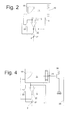
- Fig. 2 shows the controller circuit 11 and circuitry connecting it to a common column electrode 2 according to a second embodiment of the invention.
- the structure of the pixel circuits 1 and the row selection circuits 17 in this second embodiment is the same as in the first one and is not shown and described again.
- the two operational amplifiers 14, 16 are replaced by a single operational amplifier 20 and first and second switches 21, 22, of which the first one 21 is provided between an output terminal of operational amplifier 20 and the common column electrode 2, and the second one 22 is provided between the common column electrode 2 and a non-inverting input terminal of amplifier 20.
- the output terminal of amplifier 20 is further directly connected to feedback input terminal 15 of controller circuit 11.
- switch 21 is closed and switch 22 is open, causing the operational amplifier 20 to assume the functions of first amplifier 14 of Fig. 1.
- switch 22 is closed, and switch 21 is open, causing amplifier 20 to assume the functions of second amplifier 16 of Fig. 1. Since the two amplifiers 14, 16 of Fig. 1 must not operate simultaneously anyway, the embodiment of Fig. 2 very conveniently reduces hardware complexity without reducing the performance of the display.
- Fig. 3 illustrates a third embodiment of the display in a block diagram analogous to Fig. 1.
- a resistor 24 is provided between each common column electrode 2 and the ground potential, and all OLEDs 8 have a common cathode 25 which is formed by a transparent thin metal layer extending all over the substrate, which is coupled to ground by a fourth switch 26 controlled by controller circuit 11.
- controller circuit 11 When the third switch 23 is open and the fourth switch 26 is closed, the display of Fig. 3 is capable of operating just as described with respect to Fig. 1.
- Vth can be reliably obtained for every drive transistor (7) regardless of a possible drift of the current-voltage characteristic of the OLEDs 8.
- Fig. 3 may be simplified in analogy to Fig. 2 by substituting a single operational amplifier 20 and first and second switches 21, 22 for the two amplifiers 14, 16 of Fig. 3. It should be noted that in this embodiment, there are no more third switches 23, either, since in the circuit design of Fig. 4, in programming operation mode, with switch 21 closed and switch 22 open, switch 22 separates resistor 25 from column electrode 2, so that no drain current Id from drive transistor 7 is lost to resistor 25, and the entire drain current Id passes OLED 8 instead.
Landscapes
- Engineering & Computer Science (AREA)
- Physics & Mathematics (AREA)
- Computer Hardware Design (AREA)
- General Physics & Mathematics (AREA)
- Theoretical Computer Science (AREA)
- Control Of Indicators Other Than Cathode Ray Tubes (AREA)
Abstract
An electroluminescent display device comprises
- a plurality of pixel circuits (1) formed on a substrate and connected to a common column electrode (2),
wherein each pixel circuit (1) comprises a drive transistor (7) and an electroluminescent device (8) connected in series between first and second supply potentials (Vdd, GND) via an intermediate node (9), a voltage storage element (6) connected to a control electrode of said drive transistor (7), a first switch (5) for connecting and disconnecting said voltage storage element (6) and said column electrode (2), and a second switch (10) for connecting and disconnecting said intermediate node (9) and said column electrode (2);
- and control means (17) for closing not more than one of said first and second switches (5;10) at a time.
- a drive voltage compensator (11) comprising a memory (19) for storing a threshold voltage of the drive transistor (7).
- a plurality of pixel circuits (1) formed on a substrate and connected to a common column electrode (2),
wherein each pixel circuit (1) comprises a drive transistor (7) and an electroluminescent device (8) connected in series between first and second supply potentials (Vdd, GND) via an intermediate node (9), a voltage storage element (6) connected to a control electrode of said drive transistor (7), a first switch (5) for connecting and disconnecting said voltage storage element (6) and said column electrode (2), and a second switch (10) for connecting and disconnecting said intermediate node (9) and said column electrode (2);
- and control means (17) for closing not more than one of said first and second switches (5;10) at a time.
- a drive voltage compensator (11) comprising a memory (19) for storing a threshold voltage of the drive transistor (7).
Description
- The present invention relates to an electroluminescent display of the active matrix type.
- In active matrix electroluminescent display technology, a display comprises a large number of pixel circuits, each of which comprises an electroluminescent device, such as an OLED (Organic Light Emitting Diode) and a current modulator associated to it, which is programmable to supply its electroluminescent device with a continuous operating current. The current modulator comprises a number of transistors which must be formed on a same substrate with the respective electroluminescent devices and which must be addressable for programming. The transistors and other components of the current modulators occupy substrate space which is not available for the electroluminescent devices. In order to achieve a high luminosity of the display, the portion of the display surface occupied by the electroluminescent devices should be as high as possible. Therefore considerable development efforts have been invested in the development of simple and space-saving current modulators.
-
WO 2005/013250 describes a current modulator formed of a switch, a capacitor and a drive transistor which controls the current flowing through an OLED based on a control voltage which is selectively admitted to the storage capacitor and the control electrode of the drive transistor by the switch. This current modulator is simple and space-saving, but the image quality that can be obtained using it is not satisfactory. The reason for this is in the quality of the drive transistor. Display substrates may be based on poly-crystalline silicon (Poly-Si) or hydrogenated amorphous silicon (a-Si:H). Thin film transistors manufactured on a poly-Si substrate tend to have large manufacturing tolerances: crystal borders are distributed stochastically in the different conductivity regions of the transistors, causing performance characteristics of the transistors such as threshold voltage, slope, etc. to vary from one transistor to the next, so that the luminosity of OLEDs may be different although the same programming voltage is applied to their drive transistors. On the other hand, on a a-Si:H substrate, transistors having closely similar performance characteristics can be manufactured, but the inherent meta-stability of the amorphous silicon layer causes these performance characteristics to drift, so that a good image quality cannot be maintained for a long time. - In order to overcome these problems, display devices have been developed in which the local or temporal variability of the drive transistor threshold is compensated.
- However, any compensation which is carried out locally in the current modulator itself will undesirably increase the number of its components and, hence, the space it occupies on the display substrate.
- In order to overcome this problem, a scheme has been proposed in
WO 2005/013250 A1 , in which a feedback signal from each current modulator is supplied to compensating circuitry which is located apart from the display substrate. A disadvantage of this concept is that the number of connections between the display substrate and peripheral circuitry is considerably increased, which makes the production of such a display laborious and increases the risk of defects due to faulty contacts. - The object of the present invention is, therefore, to provide an electroluminescent display device in which locally or temporally variable thresholds of drive transistors of the electroluminescent devices are compensated for without substantially increasing the number of necessary contacts between a substrate on which the electroluminescent devices are formed and peripheral circuitry.
- The object is achieved by an electroluminescent display device comprising a plurality of pixel circuits formed on a substrate and connected to a common electrode, wherein each pixel circuit comprises a drive transistor and an electroluminescent device connected in series between first and second supply potentials via an intermediate node, a voltage storage element connected to a control electrode of said drive transistor, a first switch for connecting and disconnecting said voltage storage element and said column electrode, and a second switch, by the fact that the second switch is arranged to connect and disconnect said intermediate node and said column electrode, and that control means are provided for closing not more than one of said first and second switches at a time.
- This arrangement allows for using the common column electrode for extracting a voltage at said intermediate node, from which a threshold voltage of the drive transistor can be inferred, whenever the common column electrode is not in use for programming the pixel circuits associated to it.
- In electroluminescent diodes such as OLEDs, the luminosity is proportional to the intensity of a current flowing in the device. In order to enable the display of the invention to directly process a device current control signal representative of desired luminosities / current intensities in each of said electroluminescent devices, the display preferably further comprises a drive voltage compensator which is controlled by the device current control signal, for determining a first voltage which, when applied to the electroluminescent device of one of said pixel circuits, will cause a current of the desired intensity to flow through said electroluminescent device, and a second voltage corresponding to a voltage between the control electrode and the intermediate node of said pixel circuit in case of a current of the desired intensity flowing through its drive transistor, and outputting, at an output terminal, a sum of said first and second voltages to the control electrode.
- The first voltage may conveniently be determined based on a voltage/intensity characteristic of the OLED. The drive voltage compensator therefore preferably comprises a memory for storing a definition of such a characteristic. The definition may e. g. be in the form of an algorithm for carrying out by a digital processor or of a lookup table.
- The inventors found that for modern OLEDs, in particular those in the red to green wavelength regions, the voltage/intensity characteristic varies extremely little over the expected lifetime, so that the definition of the characteristic may be built into the drive voltage compensator at the time of manufacturing, without a need for a later update. In case of blue OLEDs, a certain aging may be observed, so that for these a possibility of updating the characteristic may be appropriate, as will be further detailed in a later section of the this description.
- Based on the voltage/intensity characteristic and a voltage applied to the OLED of the pixel circuit, it is possible to derive the second voltage mentioned above. The drive voltage compensator therefore preferably has an input connected to the common electrode for detecting the voltage applied to the OLED. Further, memory means for storing a threshold voltage obtained from the voltage applied to the OLED should be provided.
- If the characteristics of the drive transistors are homogeneous all over the substrate, in particular in case of the substrate being made of amorphous silicon, one value of the threshold voltage may be assumed to be appropriate for all drive transistors, and a same storage cell of said memory means may be associated to all pixel circuits of the display.
- On the other hand, if the characteristics of the drive transistors are not homogeneous, e. g. in case of the substrate being made of poly-Si, each pixel circuit may have a storage cell of said memory means associated to it for storing therein the threshold voltage of the drive transistor of said pixel circuit.
- If the substrate is a poly-Si substrate manufactured by annealing an amorphous silicon layer by scanning it with a laser beam, transistors formed along a scanning line of the laser beam may have rather homogeneous characteristics. In that case, storage space may be saved if the pixel circuits are divided into groups, the pixel circuits of a same group being arranged along a same line on the substrate, and a storage cell of said memory means is associated to each said groups for storing the threshold voltage.
- For quickly programming a new voltage in the voltage storage element, a charging current should be provided at low impedance. To this effect, a first amplifier may be provided which has a first input connected to the output port of the voltage compensator for receiving a voltage signal representative of a desired current intensity in the electroluminescent devices and an output coupled to the voltage storage elements. Preferably, the amplifier is selectively coupled to the voltage storage elements of all pixel circuits associated to a same common column electrode via said common column electrode.
- The first amplifier may be a differential amplifier which has a second input coupled to the common column electrode. In this way, the first amplifier may operate at unity gain.
- A second amplifier may be provided, which has an input coupled to the common column electrode and an output coupled to the input of the voltage compensator, for providing the voltage compensator with the voltage present at the intermediate node. This second amplifier may also preferably operate at unity gain, providing a signal at the voltage level of the intermediate node, to which a load may be applied without influencing the voltage at the intermediate node.
- In order to prevent the two amplifiers from influencing each other, the output of the first amplifier preferably has a high impedance state. This state can be activated when the voltage at the intermediate node is applied to the input of the second amplifier.
- In an alternative embodiment, the two amplifiers are prevented from influencing each other by implementing them in a same amplifier, which may fulfil the functions of both in a time-multiplexed manner. To this effect, the first switch is preferably provided between the output of said same amplifier and the common column electrode, and the second switch is provided between the common column electrode and the first input of the amplifier.
- In order to judge a possible drift of the characteristics of the electroluminescent devices of the pixel circuits, these devices may have a first electrode connected to the intermediate node and a second electrode connected to the second supply potential by a third switch, and a resistor provided between the first input of the first amplifier and the second supply potential allows to deviate a current flowing through the drive transistor into the resistor in order to estimate its intensity.
- The electroluminescent devices may have their second electrodes connected together, so that a single third switch connected between these second electrodes and the second supply potential is sufficient for interrupting the current in all of the electroluminescent devices.
- Further features and advantages of the invention become apparent from the subsequent description of embodiments thereof referring to the appended drawings.
- Fig. 1
- is a block diagram of an electroluminescent display according to a first embodiment of the invention;
- Fig. 2
- is a block diagram of part of the control circuitry of the display according to a second embodiment;
- Fig. 3
- is a block diagram of an electroluminescent display according to a third embodiment;
- Fig. 4
- is a block diagram of the control circuitry according to a fourth embodiment.
- Fig. 1 is a block diagram of a display device according to the present invention. It comprises a large number of
pixel circuits 1 arranged in a pattern of rows and columns on a silicon thin film substrate made of amorphous or polycrystalline silicon. In the drawing, only two rows and two columns are illustrated, but it is obvious a skilled person that an arbitrary number of rows and columns may be provided. Allpixel circuits 1 belonging to a same column are connected to acommon column electrode 2. Allpixel circuits 1 that belong to a same row are connected to a samerow selection circuit 17 by common first and second rowselect lines pixel circuit 1, the first rowselect line 3 is connected to a gate of a first thin film transistor (TFT) 5, which has one of its current electrodes connected to thecommon column electrode 2 and its other current electrode to a first plate of a storage capacitor 6 and to a gate of adrive transistor 7. Thedrive transistor 7 has its drain connected to the other plate of the storage capacitor 6 and to a positive supply potential Vdd, whereas its source is connected to the anode of an OLED 8 via an intermediate node 9. The cathode of theOLED 8 is connected to ground GND. - The second row
select line 4 is connected to a gate of asecond TFT 10 in each pixel circuit. Current electrodes of the second TFT are connected to thecolumn electrode 2 of thepixel circuit 1, on the one hand, and to the intermediate node 9 thereof, on the other. - A
controller circuit 11 has aninput terminal 12 for receiving a video signal VIDEO of arbitrary conventional type which specifies a desired luminosity of each of theOLEDs 8, and a plurality ofoutput terminals 13, each of which is coupled to an associated one of thecommon column electrodes 2 by a firstoperational amplifier 14. Theoperational amplifier 14 has its output terminal connected to an inverting input terminal, so as to provide unity gain. Thecontroller circuit 11 further has a plurality offeedback input terminals 15, one per column, each of which is coupled to thecommon column electrode 2 associated to it by a secondoperational amplifier 16. Theamplifiers 16, too, have their output terminals connected to respective inverting input terminals, so as to provide unity gain. - Based on desired intensity information it extracts from the input video signal VIDEO for a given row of
pixel circuits 1, thecontroller circuit 11 derives a programming voltage Vdata for eachpixel circuit 1 of that row, which is representative of the desired luminosity of theOLED 8 of that pixel circuit. Thefirst amplifier 14 outputs the programming voltages Vdata to eachcolumn electrode 2. Therow selection circuit 17 of the row to which the output programming voltages Vdata correspond controls thefirst TFTs 5 of that row to be conductive, whereas thesecond TFTs 10 of that row and first and second TFTs of all other rows are kept non-conductive. Thus, in eachpixel circuit 1 of that row the programming voltage Vdata is applied to the first plate of the storage capacitor 6 and to the gate ofdrive transistor 7. After a short time, thefirst TFT 5 is made non-conductive again, so that the programming voltage Vdata remains stored in the storage capacitor 6 and continues to be applied to the gate ofdrive transistor 7. - Between the gate and the source of
drive transistor 7, there is a voltage drop VGS, so that the voltage at intermediate node 9 is Vdata-VGS=VOLED. The luminosity of eachOLED 8 is directly proportional to the current IOLED flowing through it, and the current IOLED is a function of VOLED which varies very little during the lifetime of the OLED. The drain current Id of thedrive transistor 7 is identical to IOLED. If it is assumed thatdrive transistor 7 is operating in the saturation region, the following equation holds:
wherein VGS is the gate-source-voltage of thetransistor 7; Vth is its threshold voltage and K is an empirical constant of thetransistor 7. - In order to program a voltage Vdata into a
pixel circuit 1 which will cause itsOLED 8 to generate a luminosity as specified by the input video signal VIDEO, thecontroller circuit 11 determines the programming voltage Vdata for eachpixel circuit 1 as follows: based on the desired luminosity of theOLED 8, an appropriate OLED current IOLED is determined. Based on the current/voltage characteristic of the OLEDs, which may be represented in amemory 18 ofcontrol circuit 11 in the form of a look-up table or of an algorithm, thecontroller circuit 11 determines an appropriate OLED voltage VOLED. In order to provide this voltage at the intermediate node, the programming voltage Vdata output bycontroller circuit 11 must compensate the gate-source voltage drop VGS ofdrive transistor 7, i. e.
must hold. Threshold voltages Vth of eachdrive transistor 7 are stored in astorage 19 ofcontroller circuit 11, enablingcontroller circuit 11 to calculate VGS according to the formula
- In other words, if the threshold voltages Vth of the
drive transistors 7 are known and stored instorage 19, thecontroller circuit 11 is able to provide a programming voltage Vdata that will yield correct luminosity values for the OLED of eachpixel circuit 1, regardless of variations of the threshold voltage between thedrive transistor 7 ofdifferent pixel circuits 1. - The threshold voltages of said
drive transistors 7 are obtained in an initialisation procedure which will be described in the following. The initialisation procedure does not have to be carried out at the frame rate or image rate of the input video signal VIDEO; it is sufficient to carry it out e.g. whenever the display is switched on. - Upon initialisation, each
pixel circuit 1 is first supplied with a programming voltage Vdata of arbitrary value. When Vdata has been stored in storage capacitor 6 of a givenpixel circuit 1, and itsfirst TFT 5 has become non-conductive,amplifier 14 associated to thecommon column electrode 2 of that pixel circuit is controlled to assume a high impedance state at its output, androw selection circuit 17 activates second rowselect line 4, causingsecond TFT 10 to become conductive, whereby the voltage VOLED at intermediate node 9 is output tocommon column electrode 2.Second amplifier 16 inputs VOLED into one offeedback input terminals 15 ofcontroller circuit 11. Based on Vdata and VOLED being known,controller circuit 11 calculates the gate-source voltage VGS of drive transistor 7:
- Based on the current-voltage characteristic of the
OLEDs 8 stored inmemory 18,controller circuit 11 determines the drain current of drive transistor 7:
- The threshold voltage Vth of
drive transistor 7 is then obtained by
- The threshold voltage Vth is written into storage cells of a
memory 19 for eachdrive transistor 7. - The above-described initialisation can be shortened if the
drive transistors 7 are formed along laser scanning lines on a poly-Si substrate obtained by laser annealing of an amorphous silicon layer. In this case, since annealing conditions are homogeneous along a scanning line, performance characteristics of a group of transistors formed along a same scanning line are closely similar, so that it is sufficient to determine the threshold voltage only for one of these transistors and to use the obtained threshold voltage later for driving all transistors of the group. - If the
pixel circuits 1 are formed on a substrate of amorphous silicon, threshold voltages of thedrive transistor 7 are likely to be closely similar to one another, but they tend to drift over the lifetime of the display. In that case, the initialisation may be reduced to determining the threshold voltage Vth of just one of thedrive transistors 7, so that during normal operation the programming voltage Vdata is calculated based on this threshold voltage Vth for all drivetransistors 7 of the display. - Fig. 2 shows the
controller circuit 11 and circuitry connecting it to acommon column electrode 2 according to a second embodiment of the invention. The structure of thepixel circuits 1 and therow selection circuits 17 in this second embodiment is the same as in the first one and is not shown and described again. In this second embodiment, the twooperational amplifiers second switches first one 21 is provided between an output terminal of operational amplifier 20 and thecommon column electrode 2, and thesecond one 22 is provided between thecommon column electrode 2 and a non-inverting input terminal of amplifier 20. The output terminal of amplifier 20 is further directly connected tofeedback input terminal 15 ofcontroller circuit 11. Under programming operation, switch 21 is closed and switch 22 is open, causing the operational amplifier 20 to assume the functions offirst amplifier 14 of Fig. 1. During the initialisation procedure, switch 22 is closed, and switch 21 is open, causing amplifier 20 to assume the functions ofsecond amplifier 16 of Fig. 1. Since the twoamplifiers - Fig. 3 illustrates a third embodiment of the display in a block diagram analogous to Fig. 1. In this embodiment, a
resistor 24 is provided between eachcommon column electrode 2 and the ground potential, and allOLEDs 8 have acommon cathode 25 which is formed by a transparent thin metal layer extending all over the substrate, which is coupled to ground by afourth switch 26 controlled bycontroller circuit 11. When thethird switch 23 is open and thefourth switch 26 is closed, the display of Fig. 3 is capable of operating just as described with respect to Fig. 1. On the other hand, when theswitch 23 of each column is closed and thefourth switch 26 is open, the current flow through theOLEDs 8 is interrupted, and the drain currents ld ofdrive transistors 7 of a row ofpixel circuits 1 specified by activating one of the second rowselect lines 4 will flow through the respective associatedthird switch 23 andresistor 24 to ground. The voltage drop Vr thus caused atresistor 24 is applied to thefeedback input terminals 15 ofcontroller circuit 11 bysecond amplifiers 16. Since currents through theresistors 24 are identical to the drain currents Id of their associateddrive transistors 7, i.e.
applies instead of eq. (2), while eq. (3) still holds, Vth can be reliably obtained for every drive transistor (7) regardless of a possible drift of the current-voltage characteristic of theOLEDs 8. This makes the embodiment particularly suited ifOLEDs 8 are used that have a current-voltage characteristic which drifts noticeably with time, as may occur with blue OLEDs according to present-day technology. - Comparing the voltages Vr thus obtained to the OLED voltages VOLED which are applied to the
feedback input terminals 15 when third switches 23 are open andfourth switch 26 is closed enables thecontroller circuit 11 to update the current-voltage characteristic of theOLEDs 8 stored inmemory 18. - As indicated in Fig. 4, the embodiment of Fig. 3 may be simplified in analogy to Fig. 2 by substituting a single operational amplifier 20 and first and
second switches amplifiers third switches 23, either, since in the circuit design of Fig. 4, in programming operation mode, withswitch 21 closed and switch 22 open,switch 22 separates resistor 25 fromcolumn electrode 2, so that no drain current Id fromdrive transistor 7 is lost toresistor 25, and the entire drain current Id passesOLED 8 instead.
Claims (14)
- An electroluminescent display device comprising- a plurality of pixel circuits (1) formed on a substrate and connected to a common column electrode (2),
wherein each pixel circuit (1) comprises a drive transistor (7) and an electroluminescent device (8) connected in series between first and second supply potentials (Vdd, GND) via an intermediate node (9), a voltage storage element (6) connected to a control electrode of said drive transistor (7), a first switch (5) for connecting and disconnecting said voltage storage element (6) and said column electrode (2), and a second switch (10) for connecting and disconnecting said intermediate node (9) and said column electrode (2);- and control means (17) for closing not more than one of said first and second switches (5; 10) at a time. - The electroluminescent display of claim 1, further comprising a drive voltage compensator (11) controlled by a device current control signal (VIDEO) representative of desired current intensities in each of said electroluminescent devices (8), for determining a first voltage (VOLED) which, when applied to the electroluminescent device (8) of one of said pixel circuits (1), will cause a current of the desired intensity (IOLED) to flow through said electroluminescent device (8), and a second voltage (Vcs) corresponding to a voltage between the control electrode and the intermediate node (9) of said pixel circuit (1) in case of a current of the desired intensity (Id) flowing through its drive transistor (7), and outputting, at an output terminal (13), a sum of said first and second voltages to the control electrode.
- The electroluminescent display of claim 2, wherein said drive voltage compensator (11) comprises a memory (18) for storing a definition of a voltage/intensity characteristic of said electroluminescent device.
- The electroluminescent display of claim 3, wherein said drive voltage compensator (11) has a feedback input (15) connected to said common column electrode (2) for detecting a voltage (VOLED) applied to the electroluminescent device (8) of said pixel circuit (1) and memory means (19) for storing a threshold voltage (Vth) of the drive transistor (7) of said pixel circuit (1) derived from said voltage (VOLED) applied to the electroluminescent device (8).
- The electroluminescent display of claim 4, wherein said memory means (19) comprises a storage cell for storing the threshold voltage (Vth) associated to all pixel circuits.
- The electroluminescent display of claim 4, wherein each pixel circuit has a storage cell of said memory means (19) associated to it for storing the threshold voltage (Vth) of said pixel circuit (1).
- The electroluminescent display of claim 4, wherein the pixel circuits (1) are divided into groups, the pixel circuits (1) of a same group being arranged along a same line on the substrate, and a storage cell of said memory means (19) is associated to each of said groups for storing the threshold voltage (Vth).
- The electroluminescent display of any of claims 2 to 7, further comprising a first amplifier (14) having a first input connected to said output port (13) of the voltage compensator (11) for receiving a voltage signal (Vdata) representative of desired current intensities in said electroluminescent devices (8) and an output coupled to said voltage storage element (6).
- The electroluminescent display of claim 8, wherein the first amplifier (14) is a differential amplifier and has a second input coupled to said common column electrode (2).
- The electroluminescent display of claim 8 or 9, further comprising a second amplifier (16) having an input coupled to said common column electrode (2) and an output coupled to the feedback input (15) of the voltage compensator (11).
- The electroluminescent display of claim 10, wherein the output of the first amplifier (14) has a high-impedance state.
- The electroluminescent display of claim 10, wherein said first and second amplifiers are a same amplifier (20), further comprising a first switch (21) installed between the output of said same amplifier (20) and said common column electrode (2), and a second switch (22) installed between the common column electrode (2) and said first input.
- The electroluminescent display of any one of the preceding claims, wherein the electroluminescent device (8) of each pixel circuit (1) has a first electrode connected to said intermediate node (9) and a second electrode (25) connected to said second supply potential (GND) by a switch (26), and a resistor (25) and another switch (23; 22) are provided in series between the common column electrode (2) and said second supply potential (GND).
- The OLED display of claim 13, wherein the electroluminescent devices (8) have their second electrodes (25) in common.
Priority Applications (1)
| Application Number | Priority Date | Filing Date | Title |
|---|---|---|---|
| EP06300786A EP1879171A1 (en) | 2006-07-10 | 2006-07-10 | Organic electroluminescent display |
Applications Claiming Priority (1)
| Application Number | Priority Date | Filing Date | Title |
|---|---|---|---|
| EP06300786A EP1879171A1 (en) | 2006-07-10 | 2006-07-10 | Organic electroluminescent display |
Publications (1)
| Publication Number | Publication Date |
|---|---|
| EP1879171A1 true EP1879171A1 (en) | 2008-01-16 |
Family
ID=37460933
Family Applications (1)
| Application Number | Title | Priority Date | Filing Date |
|---|---|---|---|
| EP06300786A Withdrawn EP1879171A1 (en) | 2006-07-10 | 2006-07-10 | Organic electroluminescent display |
Country Status (1)
| Country | Link |
|---|---|
| EP (1) | EP1879171A1 (en) |
Cited By (4)
| Publication number | Priority date | Publication date | Assignee | Title |
|---|---|---|---|---|
| EP2081177A3 (en) * | 2008-01-21 | 2009-12-16 | Samsung Mobile Display Co., Ltd. | Organic light emitting display and method of driving the same |
| JP2011170313A (en) * | 2010-02-19 | 2011-09-01 | Samsung Mobile Display Co Ltd | Display device and driving method thereof |
| CN104361861A (en) * | 2014-11-20 | 2015-02-18 | 昆山国显光电有限公司 | Organic electroluminescent device |
| WO2024139025A1 (en) * | 2022-12-26 | 2024-07-04 | 惠科股份有限公司 | Pixel driving circuit, resistance compensation method, and display panel |
Citations (4)
| Publication number | Priority date | Publication date | Assignee | Title |
|---|---|---|---|---|
| US20040046719A1 (en) * | 2002-08-16 | 2004-03-11 | Wen-Chun Wang | Active organic light emitting diode drive circuit |
| FR2857146A1 (en) * | 2003-07-03 | 2005-01-07 | Thomson Licensing Sa | Organic LED display device for e.g. motor vehicle, has operational amplifiers connected between gate and source electrodes of modulators, where counter reaction of amplifiers compensates threshold trigger voltages of modulators |
| WO2005109389A1 (en) * | 2004-05-06 | 2005-11-17 | Thomson Licensing | Circuit and control method for a light-emitting display |
| US20060139253A1 (en) * | 2004-12-24 | 2006-06-29 | Choi Sang M | Pixel and light emitting display |
-
2006
- 2006-07-10 EP EP06300786A patent/EP1879171A1/en not_active Withdrawn
Patent Citations (4)
| Publication number | Priority date | Publication date | Assignee | Title |
|---|---|---|---|---|
| US20040046719A1 (en) * | 2002-08-16 | 2004-03-11 | Wen-Chun Wang | Active organic light emitting diode drive circuit |
| FR2857146A1 (en) * | 2003-07-03 | 2005-01-07 | Thomson Licensing Sa | Organic LED display device for e.g. motor vehicle, has operational amplifiers connected between gate and source electrodes of modulators, where counter reaction of amplifiers compensates threshold trigger voltages of modulators |
| WO2005109389A1 (en) * | 2004-05-06 | 2005-11-17 | Thomson Licensing | Circuit and control method for a light-emitting display |
| US20060139253A1 (en) * | 2004-12-24 | 2006-06-29 | Choi Sang M | Pixel and light emitting display |
Cited By (7)
| Publication number | Priority date | Publication date | Assignee | Title |
|---|---|---|---|---|
| EP2081177A3 (en) * | 2008-01-21 | 2009-12-16 | Samsung Mobile Display Co., Ltd. | Organic light emitting display and method of driving the same |
| CN101494023B (en) * | 2008-01-21 | 2011-12-14 | 三星移动显示器株式会社 | Organic light emitting display and method of driving the same |
| JP2011170313A (en) * | 2010-02-19 | 2011-09-01 | Samsung Mobile Display Co Ltd | Display device and driving method thereof |
| US8896585B2 (en) | 2010-02-19 | 2014-11-25 | Samsung Display Co., Ltd. | Display device and driving method thereof |
| CN104361861A (en) * | 2014-11-20 | 2015-02-18 | 昆山国显光电有限公司 | Organic electroluminescent device |
| CN104361861B (en) * | 2014-11-20 | 2017-10-10 | 昆山国显光电有限公司 | A kind of Organnic electroluminescent device |
| WO2024139025A1 (en) * | 2022-12-26 | 2024-07-04 | 惠科股份有限公司 | Pixel driving circuit, resistance compensation method, and display panel |
Similar Documents
| Publication | Publication Date | Title |
|---|---|---|
| JP5118312B2 (en) | Active matrix display and driving method | |
| US7199768B2 (en) | Display apparatus controlling brightness of current-controlled light emitting element | |
| EP2232557B1 (en) | Pixel circuit | |
| JP5618170B2 (en) | Electroluminescence display device | |
| KR100968252B1 (en) | Method for detecting light emitting elements of active matrix display pixel cells, active matrix display devices and pixel cells in active matrix display devices | |
| JP4559847B2 (en) | Display device using organic light emitting element | |
| US7554514B2 (en) | Electro-optical device and electronic apparatus | |
| JP5144262B2 (en) | Method for driving an element of an electroluminescent display and circuit for an element of an electroluminescent display | |
| JP5184625B2 (en) | Display panel device and control method thereof | |
| US7248255B2 (en) | Active drive type light emitting display device and drive control method thereof | |
| US8294737B2 (en) | Display apparatus and display-apparatus driving method | |
| US20040095168A1 (en) | Electronic circuit, method of driving electronic circuit, electronic device, electro-optical device, method of driving electro-optical device, and electronic apparatus | |
| KR20070029539A (en) | Display circuitry and control circuitry for the optical modulator | |
| JP2010281914A (en) | Display device, display device driving method, and electronic apparatus | |
| CN105453164A (en) | Brightness deviation compensation apparatus and compensation method of display device | |
| US7427970B2 (en) | Circuit for driving light emitting element and current-control-type light-emitting display | |
| KR20080090954A (en) | Pixel driving method and apparatus of organic light emitting display device | |
| KR100813097B1 (en) | Pixel circuit, data driving circuit and organic light emitting display device including the same | |
| US7573442B2 (en) | Display, active matrix substrate, and driving method | |
| KR100744402B1 (en) | Data drive | |
| KR20250041674A (en) | Display device and method of driving display device | |
| KR100655779B1 (en) | Precharge Circuit for AMOLED |
Legal Events
| Date | Code | Title | Description |
|---|---|---|---|
| PUAI | Public reference made under article 153(3) epc to a published international application that has entered the european phase |
Free format text: ORIGINAL CODE: 0009012 |
|
| AK | Designated contracting states |
Kind code of ref document: A1 Designated state(s): AT BE BG CH CY CZ DE DK EE ES FI FR GB GR HU IE IS IT LI LT LU LV MC NL PL PT RO SE SI SK TR |
|
| AX | Request for extension of the european patent |
Extension state: AL BA HR MK YU |
|
| AKX | Designation fees paid | ||
| STAA | Information on the status of an ep patent application or granted ep patent |
Free format text: STATUS: THE APPLICATION IS DEEMED TO BE WITHDRAWN |
|
| 18D | Application deemed to be withdrawn |
Effective date: 20080717 |
|
| REG | Reference to a national code |
Ref country code: DE Ref legal event code: 8566 |