EP1878999A1 - Semiconductor substrate for interferometer fiber optic gyroscopes - Google Patents
Semiconductor substrate for interferometer fiber optic gyroscopes Download PDFInfo
- Publication number
- EP1878999A1 EP1878999A1 EP07106155A EP07106155A EP1878999A1 EP 1878999 A1 EP1878999 A1 EP 1878999A1 EP 07106155 A EP07106155 A EP 07106155A EP 07106155 A EP07106155 A EP 07106155A EP 1878999 A1 EP1878999 A1 EP 1878999A1
- Authority
- EP
- European Patent Office
- Prior art keywords
- wave guide
- substrate
- gyroscope
- fiber
- light source
- Prior art date
- Legal status (The legal status is an assumption and is not a legal conclusion. Google has not performed a legal analysis and makes no representation as to the accuracy of the status listed.)
- Withdrawn
Links
- 239000000758 substrate Substances 0.000 title claims abstract description 118
- 239000000835 fiber Substances 0.000 title claims abstract description 14
- 239000004065 semiconductor Substances 0.000 title abstract description 43
- 230000003287 optical effect Effects 0.000 claims description 14
- 238000005530 etching Methods 0.000 claims description 8
- 238000010894 electron beam technology Methods 0.000 claims description 7
- 238000004891 communication Methods 0.000 claims description 5
- 239000011521 glass Substances 0.000 claims description 5
- 238000007740 vapor deposition Methods 0.000 claims description 4
- 230000035945 sensitivity Effects 0.000 claims description 3
- 238000000034 method Methods 0.000 abstract description 25
- 238000001465 metallisation Methods 0.000 description 12
- 230000008569 process Effects 0.000 description 12
- 239000000463 material Substances 0.000 description 9
- 230000000873 masking effect Effects 0.000 description 8
- 238000010586 diagram Methods 0.000 description 5
- 239000013307 optical fiber Substances 0.000 description 5
- 230000005540 biological transmission Effects 0.000 description 4
- 150000001875 compounds Chemical class 0.000 description 4
- 238000004519 manufacturing process Methods 0.000 description 4
- 238000005259 measurement Methods 0.000 description 4
- 230000010363 phase shift Effects 0.000 description 4
- 229910000980 Aluminium gallium arsenide Inorganic materials 0.000 description 2
- 229910001218 Gallium arsenide Inorganic materials 0.000 description 2
- 230000001133 acceleration Effects 0.000 description 2
- 238000013461 design Methods 0.000 description 2
- 230000000694 effects Effects 0.000 description 2
- 238000005305 interferometry Methods 0.000 description 2
- 238000000059 patterning Methods 0.000 description 2
- 230000002093 peripheral effect Effects 0.000 description 2
- 238000003860 storage Methods 0.000 description 2
- 239000003039 volatile agent Substances 0.000 description 2
- 241000256837 Apidae Species 0.000 description 1
- 241000257159 Musca domestica Species 0.000 description 1
- XUIMIQQOPSSXEZ-UHFFFAOYSA-N Silicon Chemical compound [Si] XUIMIQQOPSSXEZ-UHFFFAOYSA-N 0.000 description 1
- FTWRSWRBSVXQPI-UHFFFAOYSA-N alumanylidynearsane;gallanylidynearsane Chemical compound [As]#[Al].[As]#[Ga] FTWRSWRBSVXQPI-UHFFFAOYSA-N 0.000 description 1
- 210000003484 anatomy Anatomy 0.000 description 1
- 238000013459 approach Methods 0.000 description 1
- 239000003990 capacitor Substances 0.000 description 1
- 230000008859 change Effects 0.000 description 1
- 239000007795 chemical reaction product Substances 0.000 description 1
- 238000004590 computer program Methods 0.000 description 1
- 239000004020 conductor Substances 0.000 description 1
- 238000010276 construction Methods 0.000 description 1
- 230000008878 coupling Effects 0.000 description 1
- 238000010168 coupling process Methods 0.000 description 1
- 238000005859 coupling reaction Methods 0.000 description 1
- 238000013500 data storage Methods 0.000 description 1
- 230000003247 decreasing effect Effects 0.000 description 1
- 239000003814 drug Substances 0.000 description 1
- 238000005265 energy consumption Methods 0.000 description 1
- 230000006870 function Effects 0.000 description 1
- 238000005286 illumination Methods 0.000 description 1
- 230000010354 integration Effects 0.000 description 1
- 230000003993 interaction Effects 0.000 description 1
- 229910052751 metal Inorganic materials 0.000 description 1
- 239000002184 metal Substances 0.000 description 1
- 238000004806 packaging method and process Methods 0.000 description 1
- 230000004044 response Effects 0.000 description 1
- 230000035939 shock Effects 0.000 description 1
- 229910052710 silicon Inorganic materials 0.000 description 1
- 239000010703 silicon Substances 0.000 description 1
Images


Classifications
-
- G—PHYSICS
- G01—MEASURING; TESTING
- G01C—MEASURING DISTANCES, LEVELS OR BEARINGS; SURVEYING; NAVIGATION; GYROSCOPIC INSTRUMENTS; PHOTOGRAMMETRY OR VIDEOGRAMMETRY
- G01C19/00—Gyroscopes; Turn-sensitive devices using vibrating masses; Turn-sensitive devices without moving masses; Measuring angular rate using gyroscopic effects
- G01C19/58—Turn-sensitive devices without moving masses
- G01C19/64—Gyrometers using the Sagnac effect, i.e. rotation-induced shifts between counter-rotating electromagnetic beams
- G01C19/72—Gyrometers using the Sagnac effect, i.e. rotation-induced shifts between counter-rotating electromagnetic beams with counter-rotating light beams in a passive ring, e.g. fibre laser gyrometers
- G01C19/721—Details, e.g. optical or electronical details
- G01C19/722—Details, e.g. optical or electronical details of the mechanical construction
Definitions
- a fiber optic gyroscope contains a coil (for example, up to 2 miles) of wound optical fiber.
- FOGS measure angular rotation by determining the phase difference in light waves that propagates in opposite directions through the coil of optical fiber. Light waves that propagate through the coil in the opposite direction of the rotation take a shorter time than light waves that propagate in the direction of rotation.
- an optical system with a beam splitter directs two light beams on a photodetector.
- the phase shift between the two beams is 180°; the two beams cancel each other and output photocurrent is minimized.
- FOGs provide extremely precise rotational rate information, due in part to a lack of cross-axis sensitivity to vibration, acceleration, and shock. FOGs will typically show higher resolution than a traditional ring laser gyroscope, and are commonly used to measure rotation in navigation applications such as aircraft, missiles, satellites, and other vehicles.
- the original phase shift changes.
- This phase shift change occurs because of an increase in the light path for one beam and a decrease in the light path for another beam.
- the photodetectors current responds to the increased illumination and becomes larger. This is typically known as the Sagnac effect.
- ring interferometry involves a beam of light (for example, a laser) split into two beams.
- the two beams are made to follow a trajectory in opposite directions.
- the trajectory must enclose an area.
- light inside the laser cavity is several frequencies at first, and one frequency quickly outperforms other frequencies (after that the light is monochromatic).
- the frequency that outperforms the others fits well in the laser cavity; a multiple of its wavelength is the length of the cavity.
- the laser process generates two frequencies of laser light.
- the two resulting frequencies are such that at all times, the same number of cycles exist in both directions of propagation (that is, a standing wave).
- This standing wave is stationary with respect to the local inertial frame of reference when the ring laser is not rotating.
- the standing wave is also stationary with respect to the local inertial frame of reference when the ring laser interferometer is rotating. This property makes the ring interferometer the electronic counterpart of a mechanical gyroscope.
- Combining a ring interferometer with a FOG currently involves integrating a separate laser source/detector and the coil of optical fiber with a wave guide for the two light beams. Such a combination requires numerous mechanical connections. The additional interactions involved lead to decreased reliability and is prone to numerous usability and capability issues (for example, more frequent calibrations). Also, the end product is typically bulky with demanding operating requirements (for example, energy consumption). These characteristics are not conducive to many present and future applications.
- a method for forming an interferometer involves forming a ring interferometer and a fiber optic gyroscope on a single semiconductor substrate.
- the following detailed description discusses at least one embodiment for combining a ring interferometer with a fiber optic gyroscope on a semiconductor substrate.
- This combination is referred to as an interferometer fiber optic gyroscope (IFOG).
- IFOG interferometer fiber optic gyroscope
- the IFOG serves as a building block in conjunction with peripheral electronics on the same semiconductor substrate.
- the final result is a miniaturized gyroscope for a plurality of applications that require navigation-related data from a measurement device.
- Application possibilities range from unaccompanied navigation drones and ballistic trajectory measurement sensors to physiological data recorders for anatomy studies.
- FIG. 1 is a block diagram of an embodiment of an electronic package assembly 100 incorporating an IFOG.
- Electronic package assembly 100 comprises device substrate 102, IFOG substrate 104, and substrate logic components 106.
- Examples of electronic package assembly 100 include any logic device such as an application-specific integrated circuit (ASIC) and the like.
- Device substrate 102 is composed of electrically conductive material known to one of skill in the art of conventional semiconductor wafer fabrication.
- IFOG substrate 104 resides within device substrate 102 and is in communication with substrate logic components 106 along communication interface 108.
- Substrate logic components 106 include, but are not limited to, peripheral electronic components known to one of skill in the art.
- substrate logic components 106 include resistors, transistors, capacitors, inductors, etc.
- IFOG substrate 104 is formed on one or more semiconductor chip die substrates using conventional semiconductor wafer fabrication methods. It is noted that for simplicity in description, a single IFOG substrate 104 is shown in FIG. 1. However, it is understood that device substrate 102 is capable of accommodating any appropriate number of IFOG substrates 104 (for example, at least one IFOG substrate in a single device substrate 102). IFOG substrate 104 is described in further detail below with respect to FIG. 2.
- electronic package assembly 100 is incorporated into one or more electronic devices.
- the one or more electronic devices (one example, electronic device 1404, is provided below with respect to FIG. 14) will measure location and orientation with the capabilities provided by IFOG substrate 104.
- electronic device 1404 retains a form factor suitable for use in applications requiring miniaturized navigational aids and operates with a minimal amount of power.
- Electronic package assembly 100 is suitable for packaging in a variety of electronic devices, such as low power navigation drones, ballistic tracing equipment, tracking aids for internal medicine, and the like. Incorporating the necessary components for an interferometer fiber optic gyroscope in IFOG substrate 104 eliminates integrating separate components (for example, a separate light source and detector with a separate length of optical fiber) into a hybrid system or device.
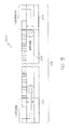
- FIG. 2 is a cross-sectional view 200 of an embodiment of IFOG substrate 104.
- IFOG substrate 104 comprises light source 202, light detector 204, wave guide coupler 206, and ring interferometer wave guide 208.
- wave guide coupler 206 further includes integrated optical circuits (IOCs) 210 1 and 210 2 .
- IOCs 210 1 and 210 2 serve as beam splitters to direct a single light beam in at least two separate and opposite directions.
- Light source wave guide 212 couples light source 202 to IOC 210 1 .
- Light detector wave guide 214 couples IOC 210 1 to light detector 204.
- IOC 210 2 is coupled to each end of ring interferometer wave guide 208.
- IOC 210 2 is a mirror image of IOC 210 1 (as illustrated in FIG. 2).
- Wave guide coupler 206 is fabricated within IFOG substrate 104 using standard semiconductor wafer fabrication processes, as further described below with respect to FIGS. 5 (9), 6 (10), 7 (11), and 8 (12).
- wave guide coupler 206, ring interferometer wave guide 208, light source wave guide 212. and light detector wave guide 214 form at least one continuous fiber-equivalent optical wave guide.
- the at least one continuous fiber-equivalent optical wave guide does not consist of optical fiber.
- ring interferometer wave guide 208 consists of a length of concentric coils whose shape is fitted to represent a ring interferometer.
- the length of concentric coils of ring interferometer wave guide 208 is at least a portion of the at least one continuous fiber-equivalent optical wave guide discussed above.
- the length of concentric coils of ring interferometer wave guide 208 reside in one or more semiconductor substrate layers for coupling with wave guide coupler 206 (as illustrated in FIG. 2).
- the length of concentric coils of ring interferometer wave guide 208 (along with light source 202, wave guide coupler 206, light source wave guide 212 and light detector wave guide 214) reside in a particular plane (for example, the x-y plane) and light detector 204 resides in a separate plane (for example, the z-plane) of a single semiconductor substrate layer.
- Wave guide coupler 206, ring interferometer wave guide 208, light source wave guide 212, and light detector wave guide 214 are formed by one or more electron-beam etching processes. At least one electron-beam etching process is described in further detail below with respect to FIGS. 3 and 4. A cross-sectional view of IFOG substrate 104 along line AA is illustrated in further detail below with respect to FIG. 13.
- IFOG substrate 104 receives electrical power to activate light source 202.
- Light source 202 emits a light beam along light source wave guide 212 and into wave guide coupler 206.
- IOC 210 2 splits the emitted light beam into two beams traveling in a clockwise (CW) and counter-clockwise (CCW) direction (as illustrated) through ring interferometer wave guide 208.
- Ring interferometer wave guide 208 encompasses an optical path represented by an area vector A .
- Wave guide coupler 206 separates the previously-emitted light beam in IOC 210 1 from at least one returning light beam of ring interferometer wave guide 208.
- ⁇ R represents a phase differential between the emitted light beam of light source 202 and the at least one returning light beam
- ⁇ represents an angular frequency of the emitted light beam of light source 202
- c represents velocity of light in a vacuum.
- ⁇ R is proportional to the rotational rate vector r combined vectorially with area vector A .
- the phase differential is used to calculate the orientation of electronic device 1404 of FIG. 14.
- the length of the concentric coils of ring interferometer wave guide 208 controls sensitivity (that is, measurement resolution) of IFOG substrate 104 based on a magnitude of area vector A .
- IFOG substrate 104 is suitable for large-scale semiconductor wafer integration. The construction of each major component of IFOG substrate 104 is described in further detail below with respect to FIGS. 3 to 12.
- FIG. 3 is a cross-sectional view of an embodiment of wave guide 206 for IFOG substrate 104 shown in a partially-formed state with a substrate structure 300 comprising at least one semiconductor substrate layer.
- Substrate structure 300 comprises IFOG substrate 104, wave guide coupler 206 (ring interferometer wave guide 208), and trough opening 302.
- wave guide coupler 206 ring interferometer wave guide 208
- a vapor deposition glass oxide creates wave guide coupler 206 (ring interferometer wave guide 208) and trough opening 302 using electron-beam etching.
- substrate structure 300 is exposed to one or more volatile agents.
- Wave guide coupler 206 (ring interferometer wave guide 208) is formed as a rounded glass trough of a number of concentric coils created by the electron-beam etching process.
- the electron-beam etching process allows a direct image of wave guide coupler 206 (ring interferometer wave guide 208) to be formed without a mask as substrate structure 300 is modified by the etching process.
- FIG. 4 is a cross-sectional view of a substrate structure 400 comprising an enclosed wave guide 206 formed on at least one semiconductor substrate layer.
- Substrate structure 400 further comprises capping material 402.
- wave guide coupler 206 (ring interferometer wave guide 208) is perfectly rounded on IFOG substrate 104 by the vapor deposition glass oxide and electron-beam etching processes.
- Wave guide coupler 206 (ring interferometer wave guide 208) is sealed with capping material 402.
- capping material 402 is constructed of an N-P doping material, a metal layer, or the like.
- FIG. 5 is a cross-sectional view of an embodiment of light source 202 for IFOG substrate 104 shown in a partially-formed state with a substrate structure 500 comprising a compound junction and at least one semiconductor substrate layer.
- Substrate structure 500 further comprises at least one field oxide layer 502 and at least one semiconductor substrate layer 504.
- the at least one field oxide layer 502 serves as at least one doping layer when light source 202 is fabricated.
- FIG. 6 is a cross-sectional view of a substrate structure 600 with an additional masking layer formed on the at least one semiconductor substrate layer 504 of FIG. 5.
- Substrate structure 600 further comprises at least one semiconductor dioxide layer 602 and at least one masking layer 604.
- the at least one semiconductor dioxide layer 602 and the at least one masking layer 604 are deposited during a series of patterning and layering operations that define a location of light source 202 on IFOG substrate 104.
- FIG. 7 is a cross-sectiorlal view of a substrate structure 700 with at least one additional doping layer formed on the at least one semiconductor substrate layer 504 of FIG. 5.
- Substrate structure 700 further comprises source P-N junction 702.
- Source P-N junction 702 is formed during at least one doping operation performed on substrate layer 600.
- the at least one doping operation creates a plurality of pockets in substrate structure 700 that are either rich in electrons (N-type) or rich in electron holes (P-type).
- the plurality of pockets forms an electricaily-active region.
- FIG. 8 is a cross-sectional view of a substrate structure 800 with an additional metallization layer formed on the at least one semiconductor substrate layer 504 of FIG. 5.
- Substrate structure 800 further comprises metallization layer 802, shown as 802 1 and 802 2 .
- substrate structure 800 represents light source 202 and light source wave guide 212, with light source wave guide 212 enclosed by capping material 402.
- Metallization layer 802 forms during an additional layering operation that provides an electrical connection for light source 202 in at least one design pattern of IFOG substrate 104.
- light source 202 comprises a laser diode on IFOG substrate 104.
- electrical current passes through substrate structure 800 from metallization layer 802 1 to metallization layer 802 2 .
- the electrical current flows through source P-N junction 702 from P-layer to N-layer, releasing electrical energy that creates a plurality of photons.
- the plurality of photons emit laser light into light source wave guide 212 (as illustrated).
- the emitted laser light from light source 202 is transferred to light detector 204 as described above with respect to FIG. 2.
- FIG. 9 is a cross-sectional view of an embodiment of light detector 204 for IFOG substrate 104 shown in a partially-formed state with a substrate structure 900 comprising a compound junction and at least one semiconductor substrate layer.
- Substrate structure 900 further comprises at least one field oxide layer 902 and at least one semiconductor layer 904.
- the at least one field oxide layer 902 serves as at least one doping layer when light detector 204 is fabricated.
- FIG. 10 is a cross-sectional view of substrate structure 1000 with at least one additional masking layer formed on the at least one semiconductor substrate layer 904 of FIG. 9.
- Substrate structure 1000 further comprises at least one semiconductor dioxide layer 1002 and at least one masking layer 1004.
- the at least one semiconductor dioxide layer 1002 and the at least one masking layer 1004 are deposited during a series of patterning and layering operations that define a location of light detector 1002 on IFOG substrate 104.
- FIG. 11 is a cross-sectional view of substrate structure 1100 with at least one additional doping layer formed on the at least one semiconductor substrate layer 904 of FIG. 9.
- Substrate structure 1100 further comprises source P-N junction 1102.
- Source P-N junction 1102 is formed during at least one doping operation performed on substrate layer 1000.
- the at least one doping operation creates a plurality of pockets in substrate structure 1100 that are either rich in electrons (N-type) or rich in electron holes (P-type).
- the plurality of pockets forms an electrically-active region.
- FIG. 12 is a cross-sectional view of substrate structure 1200 with an additional metallization layer formed on the at least one semiconductor substrate layer 904 of FIG. 9.
- Substrate structure 1200 further comprises metallization layer 1202, shown as 1202 1 and 1202 2 .
- substrate structure 1200 represents light detector 204 and light detector wave guide 214, with light detector wave guide 214 enclosed by capping material 402.
- Metallization layer 1202 forms during an additional layering operation that provides an electrical connection for light detector 204 in at least one design pattern of IFOG substrate 104.
- light detector 204 comprises a photodiode on IFOG substrate 104.
- light detector 204 detects returning laser light from light detector wave guide 214 (as illustrated).
- the returning laser light from light detector wave guide 214 flows into detector P-N junction 1102, absorbing the plurality of photons described earlier with respect to FIG. 8.
- Light detector 204 produces a photocurrent (that is, an electrical current) passing through metallization layer 1202 1 to metallization layer 1202 2 .
- assembly 100 processes the photocurrent for at least one IFOG measurement.
- FIG. 13 is a cross-sectional view of an embodiment of the substrate structure 1300 along line AA of FIG. 2 (IFOG substrate 104).
- Substrate structure 1300 comprises light source (source diode) 202, light detector (detector diode) 204 and ring interferometer wave guide 208.
- substrate structure 1300 is fabricated with one or more standard semiconductor wafer processes (for example, one or more silicon wafer fabrication methods). Alternate methods of fabricating substrate structure 1300 comprise a heterojunction composed of one or more layers of one or more dissimilar semiconductor material.
- the one or more dissimilar semiconductor materials have non-equal bandgaps (that is, energy differences between junctions).
- a sequence of aluminum gallium arsenide - gallium arsenide - aluminum gallium arsenide form a double heterojunction.
- characteristics of modem laser diodes for example, source diode 600 and detector diode 1200
- diode model parameters for source diode 600 and detector diode 1200 that define the diode current vs. voltage response are tunable by adjusting the thicknesses and bandgaps of the one or more layers of dissimilar semiconductor material.
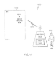
- FIG. 14 is a block diagram of an embodiment of a system 1400 for recording data with an electronic device.
- System 1400 comprises area 1402, electronic device 1404, base station 1408, and user 1412.
- base station 1408 further comprises display 1410.
- Electronic device 1404 comprises electronic package assembly 100, including at least one IFOG substrate 104, as described earlier with respect to FIG. 1.
- Examples of electronic device 1404 include, without limitation, a miniature camera, a miniature navigation drone, and a minute remote sensor suitable for providing base station 1408 with navigation-related data surrounding or within area 1402.
- electronic device 1404 is appropriately sized (for example, the size of a common housefly or a bumblebee) for unrestricted travel within area 1402.
- Electronic device 1404 is self-powered and travels throughout area 1402, continuously recording navigation-related data.
- navigation-related data is a position estimate to be determined by electronic device 1404.
- Another example of navigation-related data is an estimate of an attribute related to motion within area 1402 (for example, the distance traveled, velocity, acceleration, location, etc.)
- Wireless transmission link 1406 comprises secure wireless communication transmissions between electronic device 1404 and base station 1408. Communication between electronic device 1404 and base station 1408 over wireless transmission link 1406 occurs when electronic device 1404 is sufficiently close to base station 1408.
- display 1410 displays the navigation-related data in real time to user 1412.
- alternate methods for conveying the navigation-related data include a database, a network server, and the like.
- the methods and techniques described here may be implemented in digital electronic circuitry, or with a programmable processor (for example, a special-purpose processor or a general-purpose processor such as a computer) firmware, software, or in combinations of them.
- An apparatus embodying these techniques may include appropriate input and output devices, a programmable processor, and a storage medium tangibly embodying program instructions for execution by the programmable processor.
- a process embodying these techniques may be performed by a programmable processor executing a program of instructions to perform desired functions by operating on input data and generating appropriate output.
- the techniques may advantageously be implemented in one or more programs that are executable on a programmable system including at least one programmable processor coupled to receive data and instructions from, and to transmit data and instructions to, a data storage system, at least one input device, and at least one output device.
- a processor will receive instructions and data from a read-only memory and/or a random access memory.
- Storage devices suitable for tangibly embodying computer program instructions and data include all forms of non-volatile memory, including by way of example semiconductor memory devices, such as EPROM, EEPROM, and flash memory devices; magnetic disks such as internal hard disks and removable disks; magnetooptical disks; and DVDs. Any of the foregoing may be supplemented by, or incorporated in, electronic package assembly 100 of FIG. 1.
Landscapes
- Physics & Mathematics (AREA)
- Engineering & Computer Science (AREA)
- Optics & Photonics (AREA)
- Electromagnetism (AREA)
- Power Engineering (AREA)
- General Physics & Mathematics (AREA)
- Radar, Positioning & Navigation (AREA)
- Remote Sensing (AREA)
- Gyroscopes (AREA)
Abstract
Description
- The U.S. Government may have certain rights in the present invention under contract no. N00030-05-C-0007 (Prime) and DL-H-551019 (Subcontract) awarded by the United States Navy.
- A fiber optic gyroscope (FOG) contains a coil (for example, up to 2 miles) of wound optical fiber. FOGS measure angular rotation by determining the phase difference in light waves that propagates in opposite directions through the coil of optical fiber. Light waves that propagate through the coil in the opposite direction of the rotation take a shorter time than light waves that propagate in the direction of rotation.
- Typically, an optical system with a beam splitter directs two light beams on a photodetector. With a zero attitude rate, the phase shift between the two beams is 180°; the two beams cancel each other and output photocurrent is minimized. FOGs provide extremely precise rotational rate information, due in part to a lack of cross-axis sensitivity to vibration, acceleration, and shock. FOGs will typically show higher resolution than a traditional ring laser gyroscope, and are commonly used to measure rotation in navigation applications such as aircraft, missiles, satellites, and other vehicles.
- With the attitude rate oriented along the fiber (that is, around the coil's axis) the original phase shift changes. This phase shift change occurs because of an increase in the light path for one beam and a decrease in the light path for another beam. As a result, the photodetectors current responds to the increased illumination and becomes larger. This is typically known as the Sagnac effect.
- The Sagnac effect is illustrated in what is commonly referred to as ring interferometry. Similar to the FOG, ring interferometry involves a beam of light (for example, a laser) split into two beams. The two beams are made to follow a trajectory in opposite directions. To act as a ring, the trajectory must enclose an area. In normal laser operation, light inside the laser cavity is several frequencies at first, and one frequency quickly outperforms other frequencies (after that the light is monochromatic). The frequency that outperforms the others fits well in the laser cavity; a multiple of its wavelength is the length of the cavity. When a ring laser is rotating, the effective path lengths of the two counter-propagating beams of laser light are different. At this point, the laser process generates two frequencies of laser light. The two resulting frequencies are such that at all times, the same number of cycles exist in both directions of propagation (that is, a standing wave). This standing wave is stationary with respect to the local inertial frame of reference when the ring laser is not rotating. The standing wave is also stationary with respect to the local inertial frame of reference when the ring laser interferometer is rotating. This property makes the ring interferometer the electronic counterpart of a mechanical gyroscope.
- Combining a ring interferometer with a FOG currently involves integrating a separate laser source/detector and the coil of optical fiber with a wave guide for the two light beams. Such a combination requires numerous mechanical connections. The additional interactions involved lead to decreased reliability and is prone to numerous usability and capability issues (for example, more frequent calibrations). Also, the end product is typically bulky with demanding operating requirements (for example, energy consumption). These characteristics are not conducive to many present and future applications.
- The following specification addresses recording orientation with an electronic device. Particularly, in one embodiment, a method for forming an interferometer is provided. The method involves forming a ring interferometer and a fiber optic gyroscope on a single semiconductor substrate.
- These and other features, aspects, and advantages will become better understood with regard to the following description, appended claims, and accompanying drawings where:
- FIG. 1 is a block diagram of an embodiment of an electronic package assembly incorporating an interferometer fiber optic gyroscope;
- FIG. 2 is a block diagram of an embodiment of an interferometer fiber optic gyroscope;
- FIG. 3 is a cross-sectional view of an embodiment of a wave guide for an interferometer fiber optic gyroscope shown in a partially-formed state with a substrate structure comprising at least one semiconductor substrate layer;
- FIG. 4 is a cross-sectional view of the substrate structure of FIG. 3 comprising an enclosed wave guide formed on the at least one semiconductor substrate layer;
- FIG. 5 is a cross-sectional view of an embodiment of a light source for an interferometer fiber optic gyroscope shown in a partially-formed state with a substrate structure comprising a compound junction and at least one semiconductor substrate layer;
- FIG. 6 is a cross-sectional view of the substrate structure of FIG. 5 with at least one additional masking layer formed on the at least one semiconductor substrate layer;
- FIG. 7 is a cross-sectional view of the substrate structure of FIG. 6 with at least one additional doping layer formed on the at least one semiconductor substrate layer;
- FIG. 8 is a cross-sectional view of the substrate structure of FIG. 7 with an additional metallization layer formed on the at least one semiconductor substrate layer;
- FIG. 9 is a cross-sectional view of an embodiment of a light detector for an interferometer fiber optic gyroscope shown in a partially-formed state with a substrate structure comprising a compound junction and at least one semiconductor substrate layer;
- FIG. 10 is a cross-sectional view of the substrate structure of FIG. 9 with at least one additional masking layer formed on the at least one semiconductor substrate layer;
- FIG. I 1 is a cross-sectional view of the substrate structure of FIG. 10 with at least one additional doping layer formed on the at least one semiconductor substrate layer;
- FIG. 12 is a cross-sectional view of the substrate structure of FIG. 11 with an additional metallization layer formed on the at least one semiconductor substrate layer; and
- FIG. 13 is a cross-sectional view of an embodiment of the substrate structure of FIG. 2; and
- FIG. 14 is a block diagram of an embodiment of a system for recording orientation with an electronic device.
- Like reference numbers and designations in the various drawings indicate like elements.
- The following detailed description discusses at least one embodiment for combining a ring interferometer with a fiber optic gyroscope on a semiconductor substrate. This combination is referred to as an interferometer fiber optic gyroscope (IFOG). Advantageously, the IFOG serves as a building block in conjunction with peripheral electronics on the same semiconductor substrate. The final result is a miniaturized gyroscope for a plurality of applications that require navigation-related data from a measurement device. Application possibilities range from unaccompanied navigation drones and ballistic trajectory measurement sensors to physiological data recorders for anatomy studies.
- FIG. 1 is a block diagram of an embodiment of an
electronic package assembly 100 incorporating an IFOG.Electronic package assembly 100 comprisesdevice substrate 102, IFOGsubstrate 104, andsubstrate logic components 106. Examples ofelectronic package assembly 100 include any logic device such as an application-specific integrated circuit (ASIC) and the like.Device substrate 102 is composed of electrically conductive material known to one of skill in the art of conventional semiconductor wafer fabrication. IFOGsubstrate 104 resides withindevice substrate 102 and is in communication withsubstrate logic components 106 alongcommunication interface 108.Substrate logic components 106 include, but are not limited to, peripheral electronic components known to one of skill in the art. For example,substrate logic components 106 include resistors, transistors, capacitors, inductors, etc. formed on one or more semiconductor chip die substrates using conventional semiconductor wafer fabrication methods. It is noted that for simplicity in description, asingle IFOG substrate 104 is shown in FIG. 1. However, it is understood thatdevice substrate 102 is capable of accommodating any appropriate number of IFOG substrates 104 (for example, at least one IFOG substrate in a single device substrate 102). IFOGsubstrate 104 is described in further detail below with respect to FIG. 2. - In operation,
electronic package assembly 100 is incorporated into one or more electronic devices. The one or more electronic devices (one example,electronic device 1404, is provided below with respect to FIG. 14) will measure location and orientation with the capabilities provided byIFOG substrate 104. In one implementation,electronic device 1404 retains a form factor suitable for use in applications requiring miniaturized navigational aids and operates with a minimal amount of power.Electronic package assembly 100 is suitable for packaging in a variety of electronic devices, such as low power navigation drones, ballistic tracing equipment, tracking aids for internal medicine, and the like. Incorporating the necessary components for an interferometer fiber optic gyroscope inIFOG substrate 104 eliminates integrating separate components (for example, a separate light source and detector with a separate length of optical fiber) into a hybrid system or device. - FIG. 2 is a
cross-sectional view 200 of an embodiment ofIFOG substrate 104.IFOG substrate 104 compriseslight source 202,light detector 204,wave guide coupler 206, and ringinterferometer wave guide 208. In the example embodiment of FIG. 2,wave guide coupler 206 further includes integrated optical circuits (IOCs) 2101 and 2102. In one implementation, each of IOCs 2101 and 2102 serve as beam splitters to direct a single light beam in at least two separate and opposite directions. Light source wave guide 212 coupleslight source 202 to IOC 2101. Light detector wave guide 214 couples IOC 2101 tolight detector 204. IOC 2102 is coupled to each end of ringinterferometer wave guide 208. In one implementation, IOC 2102 is a mirror image of IOC 2101 (as illustrated in FIG. 2). Alternate implementations forwave guide coupler 206 are possible. Light source 202 (light detector 204) is fabricated withinIFOG substrate 104 using standard semiconductor wafer fabrication processes, as further described below with respect to FIGS. 5 (9), 6 (10), 7 (11), and 8 (12). In the example embodiment of FIG. 2,wave guide coupler 206, ringinterferometer wave guide 208, lightsource wave guide 212. and lightdetector wave guide 214 form at least one continuous fiber-equivalent optical wave guide. In one implementation, the at least one continuous fiber-equivalent optical wave guide does not consist of optical fiber. - In the example embodiment of FIG. 2, ring
interferometer wave guide 208 consists of a length of concentric coils whose shape is fitted to represent a ring interferometer. The length of concentric coils of ringinterferometer wave guide 208 is at least a portion of the at least one continuous fiber-equivalent optical wave guide discussed above. In one implementation, the length of concentric coils of ringinterferometer wave guide 208 reside in one or more semiconductor substrate layers for coupling with wave guide coupler 206 (as illustrated in FIG. 2). In alternate implementations, the length of concentric coils of ring interferometer wave guide 208 (along withlight source 202,wave guide coupler 206, lightsource wave guide 212 and light detector wave guide 214) reside in a particular plane (for example, the x-y plane) andlight detector 204 resides in a separate plane (for example, the z-plane) of a single semiconductor substrate layer. -
Wave guide coupler 206, ringinterferometer wave guide 208, lightsource wave guide 212, and lightdetector wave guide 214 are formed by one or more electron-beam etching processes. At least one electron-beam etching process is described in further detail below with respect to FIGS. 3 and 4. A cross-sectional view ofIFOG substrate 104 along line AA is illustrated in further detail below with respect to FIG. 13. - In operation,
IFOG substrate 104 receives electrical power to activatelight source 202.Light source 202 emits a light beam along lightsource wave guide 212 and intowave guide coupler 206. IOC 2102 splits the emitted light beam into two beams traveling in a clockwise (CW) and counter-clockwise (CCW) direction (as illustrated) through ringinterferometer wave guide 208. Ringinterferometer wave guide 208 encompasses an optical path represented by an area vectorA .Wave guide coupler 206 separates the previously-emitted light beam in IOC 2101 from at least one returning light beam of ringinterferometer wave guide 208. Oncelight detector 204 detects the at least one returning light beam on lightdetector wave guide 214,IFOG substrate 104 establishes a rotational rate vector F . After traveling through ringinterferometer wave guide 208, the at least one returning light beam experiences a phase shift (phase differential) illustrated byEquation 1 below:
- With respect to
Equation 1 above, ΔΦR represents a phase differential between the emitted light beam oflight source 202 and the at least one returning light beam, ω represents an angular frequency of the emitted light beam oflight source 202, and c represents velocity of light in a vacuum. ΔΦR is proportional to the rotational rate vectorr combined vectorially with area vectorA . In one implementation, the phase differential is used to calculate the orientation ofelectronic device 1404 of FIG. 14. The length of the concentric coils of ringinterferometer wave guide 208 controls sensitivity (that is, measurement resolution) ofIFOG substrate 104 based on a magnitude of area vectorA .IFOG substrate 104 is suitable for large-scale semiconductor wafer integration. The construction of each major component ofIFOG substrate 104 is described in further detail below with respect to FIGS. 3 to 12. - FIG. 3 is a cross-sectional view of an embodiment of
wave guide 206 forIFOG substrate 104 shown in a partially-formed state with asubstrate structure 300 comprising at least one semiconductor substrate layer.Substrate structure 300 comprisesIFOG substrate 104, wave guide coupler 206 (ring interferometer wave guide 208), andtrough opening 302. In the example embodiment of FIG. 3, a vapor deposition glass oxide creates wave guide coupler 206 (ring interferometer wave guide 208) andtrough opening 302 using electron-beam etching. In the vapor deposition glass oxide process,substrate structure 300 is exposed to one or more volatile agents. The one or more volatile agents react to (for example, decompose)substrate structure 300 enough to produce wave guide coupler 206 (ring interferometer wave guide 208) andtrough opening 302. Wave guide coupler 206 (ring interferometer wave guide 208) is formed as a rounded glass trough of a number of concentric coils created by the electron-beam etching process. The electron-beam etching process allows a direct image of wave guide coupler 206 (ring interferometer wave guide 208) to be formed without a mask assubstrate structure 300 is modified by the etching process. - FIG. 4 is a cross-sectional view of a
substrate structure 400 comprising anenclosed wave guide 206 formed on at least one semiconductor substrate layer.Substrate structure 400 further comprises cappingmaterial 402. As described above with respect to FIG. 3, wave guide coupler 206 (ring interferometer wave guide 208) is perfectly rounded onIFOG substrate 104 by the vapor deposition glass oxide and electron-beam etching processes. Wave guide coupler 206 (ring interferometer wave guide 208) is sealed with cappingmaterial 402. In the example embodiment of FIG. 4, cappingmaterial 402 is constructed of an N-P doping material, a metal layer, or the like. - FIG. 5 is a cross-sectional view of an embodiment of
light source 202 forIFOG substrate 104 shown in a partially-formed state with asubstrate structure 500 comprising a compound junction and at least one semiconductor substrate layer.Substrate structure 500 further comprises at least onefield oxide layer 502 and at least onesemiconductor substrate layer 504. The at least onefield oxide layer 502 serves as at least one doping layer whenlight source 202 is fabricated. - FIG. 6 is a cross-sectional view of a
substrate structure 600 with an additional masking layer formed on the at least onesemiconductor substrate layer 504 of FIG. 5.Substrate structure 600 further comprises at least onesemiconductor dioxide layer 602 and at least onemasking layer 604. The at least onesemiconductor dioxide layer 602 and the at least onemasking layer 604 are deposited during a series of patterning and layering operations that define a location oflight source 202 onIFOG substrate 104. - FIG. 7 is a cross-sectiorlal view of a
substrate structure 700 with at least one additional doping layer formed on the at least onesemiconductor substrate layer 504 of FIG. 5.Substrate structure 700 further comprises sourceP-N junction 702.Source P-N junction 702 is formed during at least one doping operation performed onsubstrate layer 600. The at least one doping operation creates a plurality of pockets insubstrate structure 700 that are either rich in electrons (N-type) or rich in electron holes (P-type). The plurality of pockets forms an electricaily-active region. - FIG. 8 is a cross-sectional view of a
substrate structure 800 with an additional metallization layer formed on the at least onesemiconductor substrate layer 504 of FIG. 5.Substrate structure 800 further comprises metallization layer 802, shown as 8021 and 8022. In the example embodiment of FIG. 8,substrate structure 800 representslight source 202 and lightsource wave guide 212, with lightsource wave guide 212 enclosed by cappingmaterial 402. Metallization layer 802 forms during an additional layering operation that provides an electrical connection forlight source 202 in at least one design pattern ofIFOG substrate 104. In the example embodiment of FIG. 8,light source 202 comprises a laser diode onIFOG substrate 104. - In operation, electrical current passes through
substrate structure 800 from metallization layer 8021 to metallization layer 8022. The electrical current flows through sourceP-N junction 702 from P-layer to N-layer, releasing electrical energy that creates a plurality of photons. The plurality of photons emit laser light into light source wave guide 212 (as illustrated). The emitted laser light fromlight source 202 is transferred tolight detector 204 as described above with respect to FIG. 2. - FIG. 9 is a cross-sectional view of an embodiment of
light detector 204 forIFOG substrate 104 shown in a partially-formed state with asubstrate structure 900 comprising a compound junction and at least one semiconductor substrate layer.Substrate structure 900 further comprises at least onefield oxide layer 902 and at least onesemiconductor layer 904. The at least onefield oxide layer 902 serves as at least one doping layer whenlight detector 204 is fabricated. - FIG. 10 is a cross-sectional view of
substrate structure 1000 with at least one additional masking layer formed on the at least onesemiconductor substrate layer 904 of FIG. 9.Substrate structure 1000 further comprises at least onesemiconductor dioxide layer 1002 and at least onemasking layer 1004. The at least onesemiconductor dioxide layer 1002 and the at least onemasking layer 1004 are deposited during a series of patterning and layering operations that define a location oflight detector 1002 onIFOG substrate 104. - FIG. 11 is a cross-sectional view of
substrate structure 1100 with at least one additional doping layer formed on the at least onesemiconductor substrate layer 904 of FIG. 9.Substrate structure 1100 further comprises sourceP-N junction 1102.Source P-N junction 1102 is formed during at least one doping operation performed onsubstrate layer 1000. The at least one doping operation creates a plurality of pockets insubstrate structure 1100 that are either rich in electrons (N-type) or rich in electron holes (P-type). The plurality of pockets forms an electrically-active region. - FIG. 12 is a cross-sectional view of
substrate structure 1200 with an additional metallization layer formed on the at least onesemiconductor substrate layer 904 of FIG. 9.Substrate structure 1200 further comprises metallization layer 1202, shown as 12021 and 12022. In this example embodiment,substrate structure 1200 representslight detector 204 and lightdetector wave guide 214, with lightdetector wave guide 214 enclosed by cappingmaterial 402. Metallization layer 1202 forms during an additional layering operation that provides an electrical connection forlight detector 204 in at least one design pattern ofIFOG substrate 104. In this example embodiment,light detector 204 comprises a photodiode onIFOG substrate 104. - In operation,
light detector 204 detects returning laser light from light detector wave guide 214 (as illustrated). The returning laser light from lightdetector wave guide 214 flows intodetector P-N junction 1102, absorbing the plurality of photons described earlier with respect to FIG. 8.Light detector 204 produces a photocurrent (that is, an electrical current) passing through metallization layer 12021 to metallization layer 12022. In this example embodiment,assembly 100 processes the photocurrent for at least one IFOG measurement. - FIG. 13 is a cross-sectional view of an embodiment of the
substrate structure 1300 along line AA of FIG. 2 (IFOG substrate 104).Substrate structure 1300 comprises light source (source diode) 202, light detector (detector diode) 204 and ringinterferometer wave guide 208. As described above with respect to FIGS. 3 to 12,substrate structure 1300 is fabricated with one or more standard semiconductor wafer processes (for example, one or more silicon wafer fabrication methods). Alternate methods of fabricatingsubstrate structure 1300 comprise a heterojunction composed of one or more layers of one or more dissimilar semiconductor material. The one or more dissimilar semiconductor materials have non-equal bandgaps (that is, energy differences between junctions). In one implementation, a sequence of aluminum gallium arsenide - gallium arsenide - aluminum gallium arsenide (AlGaAs - GaAs - AlGaAs) form a double heterojunction. With a heterojunction, characteristics of modem laser diodes (for example,source diode 600 and detector diode 1200) closely approach those of an idealized diode. Furthermore, diode model parameters forsource diode 600 anddetector diode 1200 that define the diode current vs. voltage response are tunable by adjusting the thicknesses and bandgaps of the one or more layers of dissimilar semiconductor material. - FIG. 14 is a block diagram of an embodiment of a
system 1400 for recording data with an electronic device.System 1400 comprisesarea 1402,electronic device 1404,base station 1408, anduser 1412. In this example embodiment,base station 1408 further comprisesdisplay 1410.Electronic device 1404 compriseselectronic package assembly 100, including at least oneIFOG substrate 104, as described earlier with respect to FIG. 1. Examples ofelectronic device 1404 include, without limitation, a miniature camera, a miniature navigation drone, and a minute remote sensor suitable for providingbase station 1408 with navigation-related data surrounding or withinarea 1402. In one implementation,electronic device 1404 is appropriately sized (for example, the size of a common housefly or a bumblebee) for unrestricted travel withinarea 1402.Electronic device 1404 is self-powered and travels throughoutarea 1402, continuously recording navigation-related data. One example of navigation-related data is a position estimate to be determined byelectronic device 1404. Another example of navigation-related data is an estimate of an attribute related to motion within area 1402 (for example, the distance traveled, velocity, acceleration, location, etc.) -
Electronic device 1404 transmits the navigation-related data alongwireless transmission link 1406.Wireless transmission link 1406 comprises secure wireless communication transmissions betweenelectronic device 1404 andbase station 1408. Communication betweenelectronic device 1404 andbase station 1408 overwireless transmission link 1406 occurs whenelectronic device 1404 is sufficiently close tobase station 1408. In one implementation,display 1410 displays the navigation-related data in real time touser 1412. In other implementations, alternate methods for conveying the navigation-related data include a database, a network server, and the like. - The methods and techniques described here may be implemented in digital electronic circuitry, or with a programmable processor (for example, a special-purpose processor or a general-purpose processor such as a computer) firmware, software, or in combinations of them. An apparatus embodying these techniques may include appropriate input and output devices, a programmable processor, and a storage medium tangibly embodying program instructions for execution by the programmable processor. A process embodying these techniques may be performed by a programmable processor executing a program of instructions to perform desired functions by operating on input data and generating appropriate output. The techniques may advantageously be implemented in one or more programs that are executable on a programmable system including at least one programmable processor coupled to receive data and instructions from, and to transmit data and instructions to, a data storage system, at least one input device, and at least one output device. Generally, a processor will receive instructions and data from a read-only memory and/or a random access memory. Storage devices suitable for tangibly embodying computer program instructions and data include all forms of non-volatile memory, including by way of example semiconductor memory devices, such as EPROM, EEPROM, and flash memory devices; magnetic disks such as internal hard disks and removable disks; magnetooptical disks; and DVDs. Any of the foregoing may be supplemented by, or incorporated in,
electronic package assembly 100 of FIG. 1.
Claims (9)
- A gyroscope (1404), comprising:a ring interferometer (104) formed in a substrate (102); anda fiber optic gyroscope formed in the same substrate (102) and in communication with the ring interferometer.
- The gyroscope (1404) of claim 1, wherein the ring interferometer (104) further comprises:at least one fiber-equivalent optical wave guide (208);a light source (202) coupled to the at least one fiber-equivalent optical wave guide (208);a light detector (204) coupled to the same at least one fiber-equivalent optical wave guide (208); and
wherein the light source (202) and the light detector (208) are coupled to the at least one fiber-equivalent optical wave guide (208) with one or more integrated optical circuits (210). - The gyroscope (1404) of claim 2, wherein the at least one fiber-equivalent optical wave guide (208) further comprises a series of concentric coils created by electron-beam etching.
- The gyroscope (1404) of claim 3, wherein a length of the series of concentric coils controls sensitivity of the ring interferometer (104).
- The gyroscope (1404) of claim 2, wherein the at least one fiber-equivalent optical wave guide (208) further comprises at least one wave guide trough (206) created with a vapor deposition glass oxide.
- The gyroscope (1404) of claim 2, wherein the light source (202) further comprises a laser diode.
- The gyroscope (1404) of claim 2, wherein the light detector (204) further comprises a photodiode.
- The gyroscope (1404) of claim 2, wherein the at least one fiber-equivalent optical wave guide (208), the light source (202), and the light detector (204) are formed on a single substrate layer.
- The gyroscope (1404) of claim 1, wherein the substrate (102) further comprises a device substrate for an application-specific integrated circuit.
Applications Claiming Priority (1)
| Application Number | Priority Date | Filing Date | Title |
|---|---|---|---|
| US11/457,680 US20080013094A1 (en) | 2006-07-14 | 2006-07-14 | Semiconductor substrate for interferometer fiber optic gyroscopes |
Publications (1)
| Publication Number | Publication Date |
|---|---|
| EP1878999A1 true EP1878999A1 (en) | 2008-01-16 |
Family
ID=38134570
Family Applications (1)
| Application Number | Title | Priority Date | Filing Date |
|---|---|---|---|
| EP07106155A Withdrawn EP1878999A1 (en) | 2006-07-14 | 2007-04-13 | Semiconductor substrate for interferometer fiber optic gyroscopes |
Country Status (3)
| Country | Link |
|---|---|
| US (1) | US20080013094A1 (en) |
| EP (1) | EP1878999A1 (en) |
| JP (1) | JP2008020435A (en) |
Cited By (2)
| Publication number | Priority date | Publication date | Assignee | Title |
|---|---|---|---|---|
| WO2009117371A1 (en) * | 2008-03-15 | 2009-09-24 | Morgan Research Corporation | Fiber laser coil form and related manufacturing techniques |
| EP2711668A1 (en) * | 2012-09-24 | 2014-03-26 | Honeywell International Inc. | Coaxial gyro accelerometer in a semiconductor substrate |
Families Citing this family (5)
| Publication number | Priority date | Publication date | Assignee | Title |
|---|---|---|---|---|
| US7929143B2 (en) * | 2008-12-08 | 2011-04-19 | Honeywell International Inc. | Integrated resonating gyro accelerometer in a semiconductor substrate |
| JP5982791B2 (en) * | 2011-11-16 | 2016-08-31 | ソニー株式会社 | Information processing apparatus, information processing method, information providing apparatus, and information providing system |
| EP3631361B1 (en) * | 2017-05-30 | 2025-01-01 | California Institute of Technology | Integrated optical gyroscope with noise cancellation |
| TWI765412B (en) | 2020-11-13 | 2022-05-21 | 國立中山大學 | Silicon photonic integrated circuit and fiber optic gyroscope apparatus |
| CN115290062B (en) * | 2022-07-05 | 2024-04-02 | 河北汉光重工有限责任公司 | Integrated small-sized optical fiber gyroscope |
Citations (2)
| Publication number | Priority date | Publication date | Assignee | Title |
|---|---|---|---|---|
| JPH0534164A (en) | 1991-07-26 | 1993-02-09 | Japan Aviation Electron Ind Ltd | Optical ring resonator of optical gyroscope |
| US7106448B1 (en) * | 2004-02-17 | 2006-09-12 | Sandia Corporation | Integrated resonant micro-optical gyroscope and method of fabrication |
Family Cites Families (6)
| Publication number | Priority date | Publication date | Assignee | Title |
|---|---|---|---|---|
| US4274742A (en) * | 1979-11-29 | 1981-06-23 | Sperry Corporation | Passive ring laser rate of turn devices |
| DE4027024A1 (en) * | 1990-08-27 | 1992-03-05 | Standard Elektrik Lorenz Ag | FIBER GYRO |
| FR2686411B1 (en) * | 1992-01-17 | 1997-03-14 | Commissariat Energie Atomique | OPTICAL GYROMETER WITH SAGNAC EFFECT IN A FULLY INTEGRATED STRUCTURE. |
| EP0964251B1 (en) * | 1997-12-15 | 2008-07-23 | Seiko Instruments Inc. | Optical waveguide probe and its manufacturing method |
| US6259089B1 (en) * | 1998-05-15 | 2001-07-10 | Rice Systems, Inc. | Integrated optics rotation sensor |
| US7228022B1 (en) * | 2005-08-16 | 2007-06-05 | The United States Of America As Represented By The Secretary Of The Navy | Polymer integrated optical transceiver |
-
2006
- 2006-07-14 US US11/457,680 patent/US20080013094A1/en not_active Abandoned
-
2007
- 2007-04-13 EP EP07106155A patent/EP1878999A1/en not_active Withdrawn
- 2007-04-13 JP JP2007105978A patent/JP2008020435A/en not_active Withdrawn
Patent Citations (2)
| Publication number | Priority date | Publication date | Assignee | Title |
|---|---|---|---|---|
| JPH0534164A (en) | 1991-07-26 | 1993-02-09 | Japan Aviation Electron Ind Ltd | Optical ring resonator of optical gyroscope |
| US7106448B1 (en) * | 2004-02-17 | 2006-09-12 | Sandia Corporation | Integrated resonant micro-optical gyroscope and method of fabrication |
Non-Patent Citations (1)
| Title |
|---|
| SILVANO DONATI: "electro optical instrumentation", 2004, PRENTICE HALL, 6109, XP002438234, 013061 * |
Cited By (3)
| Publication number | Priority date | Publication date | Assignee | Title |
|---|---|---|---|---|
| WO2009117371A1 (en) * | 2008-03-15 | 2009-09-24 | Morgan Research Corporation | Fiber laser coil form and related manufacturing techniques |
| EP2711668A1 (en) * | 2012-09-24 | 2014-03-26 | Honeywell International Inc. | Coaxial gyro accelerometer in a semiconductor substrate |
| US8873029B2 (en) | 2012-09-24 | 2014-10-28 | Honeywell International Inc. | Coaxial gyro accelerometer in a semiconductor substrate |
Also Published As
| Publication number | Publication date |
|---|---|
| JP2008020435A (en) | 2008-01-31 |
| US20080013094A1 (en) | 2008-01-17 |
Similar Documents
| Publication | Publication Date | Title |
|---|---|---|
| US10274319B2 (en) | Photonic integrated circuit for an interference fiber optic gyroscope (IFOG) | |
| US11656081B2 (en) | Integrated photonics optical gyroscopes optimized for autonomous terrestrial and aerial vehicles | |
| US7929143B2 (en) | Integrated resonating gyro accelerometer in a semiconductor substrate | |
| US10578438B2 (en) | Optical gyroscope, electro-optic system, and methods of forming the same | |
| CN101858745B (en) | All solid state micro-opto-electro-mechanical gyro based on annular resonant cavity | |
| JP2008020435A (en) | Semiconductor substrate for interferometer fiber optic gyroscope | |
| US20240068813A1 (en) | Silicon nitride waveguide based integrated photonics front-end chip for optical gyroscope | |
| US20250257999A1 (en) | Portable optical gyroscope and compass unit | |
| US8873029B2 (en) | Coaxial gyro accelerometer in a semiconductor substrate | |
| EP4121717A1 (en) | Semi-finished product for the construction of a gyroscope and gyroscope including the semi-finished product | |
| Dranitsyna et al. | Current state and development prospects of fiber-optic gyroscopes | |
| WO2023205471A1 (en) | Method for fabrication of a multiple range accelerometer | |
| Shukri et al. | Photonic integrated circuit microchip-based optical gyroscopes for high-precision inertial measurement units | |
| US9163941B2 (en) | System and method for implementing low-cost electronic gyroscopes and accelerometer | |
| US7057734B2 (en) | Integrated reaction wheel assembly and fiber optic gyro | |
| JP2009036650A (en) | Semiconductor ring laser gyro | |
| CN116086496B (en) | A method and system for improving the sensitivity of an integrated fiber optic gyroscope | |
| US12123718B1 (en) | Mitigating bias instabilities in optical gyroscopes | |
| Ruffin | Fiber gyroscope sensors | |
| JPS5966181A (en) | Integrated semiconductor laser gyro | |
| CN121702368A (en) | Triaxial integrated fiber-optic gyroscope integrated device with low electric crosstalk and fiber-optic gyroscope | |
| HK40017341B (en) | Photonic integrated circuit for an interference fiber optic gyroscope (ifog) | |
| Nielson et al. | Application Design and Fabrication Challenges and Solutions for a Fully Integrated 6-axis IMU with Timing. |
Legal Events
| Date | Code | Title | Description |
|---|---|---|---|
| PUAI | Public reference made under article 153(3) epc to a published international application that has entered the european phase |
Free format text: ORIGINAL CODE: 0009012 |
|
| AK | Designated contracting states |
Kind code of ref document: A1 Designated state(s): AT BE BG CH CY CZ DE DK EE ES FI FR GB GR HU IE IS IT LI LT LU LV MC MT NL PL PT RO SE SI SK TR |
|
| AX | Request for extension of the european patent |
Extension state: AL BA HR MK YU |
|
| 17P | Request for examination filed |
Effective date: 20080702 |
|
| 17Q | First examination report despatched |
Effective date: 20080731 |
|
| AKX | Designation fees paid |
Designated state(s): DE |
|
| STAA | Information on the status of an ep patent application or granted ep patent |
Free format text: STATUS: THE APPLICATION IS DEEMED TO BE WITHDRAWN |
|
| 18D | Application deemed to be withdrawn |
Effective date: 20101103 |