EP1876655A2 - Light emitting device housing and a manufacturing method thereof, and light emitting apparatus using the same - Google Patents
Light emitting device housing and a manufacturing method thereof, and light emitting apparatus using the same Download PDFInfo
- Publication number
- EP1876655A2 EP1876655A2 EP07013110A EP07013110A EP1876655A2 EP 1876655 A2 EP1876655 A2 EP 1876655A2 EP 07013110 A EP07013110 A EP 07013110A EP 07013110 A EP07013110 A EP 07013110A EP 1876655 A2 EP1876655 A2 EP 1876655A2
- Authority
- EP
- European Patent Office
- Prior art keywords
- light emitting
- emitting device
- concave part
- side surfaces
- silicon substrate
- Prior art date
- Legal status (The legal status is an assumption and is not a legal conclusion. Google has not performed a legal analysis and makes no representation as to the accuracy of the status listed.)
- Withdrawn
Links
Images




Classifications
-
- H—ELECTRICITY
- H10—SEMICONDUCTOR DEVICES; ELECTRIC SOLID-STATE DEVICES NOT OTHERWISE PROVIDED FOR
- H10H—INORGANIC LIGHT-EMITTING SEMICONDUCTOR DEVICES HAVING POTENTIAL BARRIERS
- H10H20/00—Individual inorganic light-emitting semiconductor devices having potential barriers, e.g. light-emitting diodes [LED]
- H10H20/80—Constructional details
- H10H20/85—Packages
- H10H20/855—Optical field-shaping means, e.g. lenses
- H10H20/856—Reflecting means
-
- H—ELECTRICITY
- H10—SEMICONDUCTOR DEVICES; ELECTRIC SOLID-STATE DEVICES NOT OTHERWISE PROVIDED FOR
- H10H—INORGANIC LIGHT-EMITTING SEMICONDUCTOR DEVICES HAVING POTENTIAL BARRIERS
- H10H20/00—Individual inorganic light-emitting semiconductor devices having potential barriers, e.g. light-emitting diodes [LED]
- H10H20/80—Constructional details
- H10H20/85—Packages
- H10H20/8506—Containers
-
- H—ELECTRICITY
- H10—SEMICONDUCTOR DEVICES; ELECTRIC SOLID-STATE DEVICES NOT OTHERWISE PROVIDED FOR
- H10W—GENERIC PACKAGES, INTERCONNECTIONS, CONNECTORS OR OTHER CONSTRUCTIONAL DETAILS OF DEVICES COVERED BY CLASS H10
- H10W72/00—Interconnections or connectors in packages
- H10W72/851—Dispositions of multiple connectors or interconnections
- H10W72/874—On different surfaces
- H10W72/884—Die-attach connectors and bond wires
-
- H—ELECTRICITY
- H10—SEMICONDUCTOR DEVICES; ELECTRIC SOLID-STATE DEVICES NOT OTHERWISE PROVIDED FOR
- H10W—GENERIC PACKAGES, INTERCONNECTIONS, CONNECTORS OR OTHER CONSTRUCTIONAL DETAILS OF DEVICES COVERED BY CLASS H10
- H10W90/00—Package configurations
-
- H—ELECTRICITY
- H10—SEMICONDUCTOR DEVICES; ELECTRIC SOLID-STATE DEVICES NOT OTHERWISE PROVIDED FOR
- H10W—GENERIC PACKAGES, INTERCONNECTIONS, CONNECTORS OR OTHER CONSTRUCTIONAL DETAILS OF DEVICES COVERED BY CLASS H10
- H10W90/00—Package configurations
- H10W90/701—Package configurations characterised by the relative positions of pads or connectors relative to package parts
- H10W90/731—Package configurations characterised by the relative positions of pads or connectors relative to package parts of die-attach connectors
- H10W90/734—Package configurations characterised by the relative positions of pads or connectors relative to package parts of die-attach connectors between a chip and a stacked insulating package substrate, interposer or RDL
-
- H—ELECTRICITY
- H10—SEMICONDUCTOR DEVICES; ELECTRIC SOLID-STATE DEVICES NOT OTHERWISE PROVIDED FOR
- H10W—GENERIC PACKAGES, INTERCONNECTIONS, CONNECTORS OR OTHER CONSTRUCTIONAL DETAILS OF DEVICES COVERED BY CLASS H10
- H10W90/00—Package configurations
- H10W90/701—Package configurations characterised by the relative positions of pads or connectors relative to package parts
- H10W90/751—Package configurations characterised by the relative positions of pads or connectors relative to package parts of bond wires
- H10W90/754—Package configurations characterised by the relative positions of pads or connectors relative to package parts of bond wires between a chip and a stacked insulating package substrate, interposer or RDL
-
- Y—GENERAL TAGGING OF NEW TECHNOLOGICAL DEVELOPMENTS; GENERAL TAGGING OF CROSS-SECTIONAL TECHNOLOGIES SPANNING OVER SEVERAL SECTIONS OF THE IPC; TECHNICAL SUBJECTS COVERED BY FORMER USPC CROSS-REFERENCE ART COLLECTIONS [XRACs] AND DIGESTS
- Y10—TECHNICAL SUBJECTS COVERED BY FORMER USPC
- Y10S—TECHNICAL SUBJECTS COVERED BY FORMER USPC CROSS-REFERENCE ART COLLECTIONS [XRACs] AND DIGESTS
- Y10S362/00—Illumination
- Y10S362/80—Light emitting diode
Definitions
- the present invention relates to a light emitting device housing and a manufacturing method thereof, and a light emitting apparatus. More specifically, it relates to a light emitting device housing including a concave part where a light emitting device is provided therein, manufacturing methods thereof, and a light emitting apparatus.
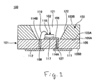
- FIG. 1 is a cross sectional view of a conventional light emitting apparatus.
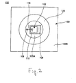
- FIG. 2 is a plan view of the light emitting apparatus shown in FIG. 1.
- a conventional light emitting apparatus 100 has awiring substrate 101, alight emitting apparatus 102, and a metal frame 103.
- the wiring substrate 101 has a main substrate 105, a wiring 106, through vias 107 and 108, and external connection terminals 111 and 112.
- the main substrate 105 is shaped in a plate form, and has through holes 114A and 114B.
- the wiring 106 is provided on the top side 105A of the main substrate 105.
- the through via 107 is provided in the through hole 114A, and is connected to the wiring 106.
- the through via 108 is provided in the through hole 114B.
- the external connection terminal 111 is provided on the back surface 105B of the main substrate 105.
- the external connection terminal 111 is connected with the through via 107.
- the external connection terminal 112 is provided on the back surface 105B of the main substrate 105.
- the external connection terminal 112 is connected with the through via 108.
- the light emitting device 102 is provided on the wiring 106.
- the light emitting device 102 has power supply terminals 117 and 118.
- the power supply terminal 117 is connected with the wiring 106, while the power supply terminal 118 is electrically connected with the through via 108 by a wire 119.
- the metal frame 103 is provided on the top side 105A of the main substrate 105.
- the metal frame 103 has an inner opening 121, and an inclined surface 122 forming the side surface of the inner opening 121.
- the inner opening 121 is formed in a taper shape such as to increase in width from the back surface 103A side of the metal frame 103 toward the top side 103B side thereof.
- the inclined surface 122 is functioning as a reflector to reflect the light emitted from the light emitting device 102 to a lens (not shown) which is disposed over the light emitting apparatus 100. Provision of such an inclined surface 122 can improve the luminous efficiency of the light emitting apparatus 100 such as known in JP-A-2004-281992 .
- the conventional light emitting apparatus 100 can be improved in luminous efficiency, it is hardly avoidable that the light emitted upwardly from the light emitting apparatus 100 would eventually diffuse. In this regard, it is not an appropriate application to use the light emitted from the light emitting apparatus 100 as a point light source.
- the light emitting apparatus serving as a point light source they can be applied for a spotlight, a headlight of a vehicle, and so on.
- the light emitting device housing according to independent claim 1 the light emitting apparatus according to claim 4, and he method for manufacturing a light emitting device housing according to independent claim 5 are provided.
- a light emitting device housing including a concave part where a light emitting device is provided therein, characterized in that the concave part has a plurality of side surfaces, at least one side surface among the plurality of the side surfaces is configured to be substantially perpendicular to the bottom surface of the concave part, and other side surfaces in said plurality of the side surfaces, in other words, other than those being configured as the perpendicular surface , are configured to be inclined surfaces to reflect the light from the light emitting device upwardly.
- the present invention makes it possible to improve the luminous efficiency by suppressing the diffusion of light emitted upwardly from the light emitting device housing.
- a method for manufacturing a light emitting device housing including a concave part provided where a light emitting device is mounted therein comprising the steps of: a silicon substrate preparation step of preparing a silicon substrate of which principal surface is a ⁇ 100> plane, a resist film formation step of forming a resist film on the principal surface of the silicon substrate, said resist film including an opening in a quadrangular shape in plan view, , and a concave part formation step of etching the silicon substrate to form the concave part by wet etching using the resist film as a mask, characterized in that forming the opening is performed in a way such that any one pair of the opposing two sides of the opening is aligned to have an angle of 45 degrees with respect to the ⁇ 110> plane of the silicon substrate.
- the concave part which has the side surfaces of the concave part made substantially perpendicular to the bottom surface of the concave part, and the side surfaces of the concave part each configured to be an inclined surface so as to reflect the light emitted from the light emitting device upwardly.
- Embodiments are also directed to apparatuses for carrying out the disclosed methods and including apparatus parts for performing described method steps. Furthermore, embodiments are also directed to methods by which the described apparatus operates or by which the described apparatus is manufactured. It may include method steps for carrying out functions of the apparatus or manufacturing parts of the apparatus. The method steps may be performed by way of hardware components, firmware, a computer programmed by appropriate software, by any combination thereof or in any other manner.
- FIG. 3 is a plan view of a light emitting apparatus in accordance with a first embodiment of the invention.
- FIG. 4 is a cross sectional view along line A-A of the light emitting apparatus shown in FIG. 3.
- a light emitting apparatus 10 of the first embodiment has a light emitting device housing 11 and a light emitting device 12.
- the light emitting device housing 11 has a housing main body 14 and via electrodes 15 and 16.
- the housing main body 14 is for housing the light emitting device 12.
- the housing main body 14 has through holes 17A and 17B, and a concave part 18.
- the through holes 17A and 17B are formed so as to penetrate through the housing main body 14.
- the concave part 18 is for housing the light emitting device 12, and has six side surfaces 18B to 18G (a plurality of side surfaces).
- the side surfaces 18B and 18C of the concave part 18 are provided so as to face any one of two long sides of the four sides of the light emitting device 12 which is a rectangle in plan configuration.
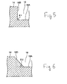
- FIG. 5 is a cross sectional view along line B-B of the light emitting apparatus shown in FIG. 3.
- the same constitutional elements as those of the light emitting apparatus 10 shown in FIG. 3 are given the same reference numerals and signs.
- the side surface 18B of the concave part 18 is configured to have a perpendicular surface substantially perpendicular to the bottom surface 18A of the concave part 18.
- the angle 01 formed between the side surface 18B and the bottom surface 18A of the concave part 18 is set to be substantially 90 degrees.
- the side surface 18C of the concave part 18 is configured to have a perpendicular surface substantially perpendicular to the bottom surface 18A of the concave part 18.
- the angle formed between the side surface 18C and the bottom surface 18A of the concave part 18 is set to be substantially 90 degrees.
- the side surfaces 18B and 18C of the concave part 18 for housing the light emitting device 12 are configured to have perpendicular surfaces made substantially perpendicular to the bottom surface 18A of the concave part 18. This can suppress the diffusion of light emitted from the light emitting apparatus 10. As a result of this, it becomes possible to allow the light emitted from the light emitting apparatus 10 to serve as a point source.
- each of the side surfaces 18B and 18C having the perpendicular surfaces is opposed to any one of two long sides of the four sides of the light emitting device 12 which is a rectangle in plan configuration. This can improve the effect of suppressing the diffusion of light emitted upwardly from the light emitting device 12.
- the ⁇ 010> planes of the silicon substrate can be utilized for the side surfaces 18B and 18C of the concave part 18, which turns out significantly improving its manufacturing productivity. This is because a method of forming the housing body 14 is directly performed on the silicon substrate, and etching the concave part of the housing body is performed by aligning one pair of the opposing two sides of the opening to have an angle of 45 degree with respect to the ⁇ 110> plane of the silicon substrate as will be explained later on.
- the side surface 18D of the concave part 18 is disposed so as to be adjacent to the side surfaces 18B and 18E of the concave part 18.
- the side surface 18E of the concave part 18 is disposed so as to be adjacent to the side surfaces 18C and 18D of the concave part 18.
- the side surfaces 18D and 18E of the concave part 18 are arranged so as to be adjacent to each other.
- the side surface 18F of the concave part 18 is disposed so as to be adjacent to the side surfaces 18B and 18G of the concave part 18.
- the side surface 18G of the concave part 18 is disposed so as to be adjacent to the side surfaces 18C and 18F of the concave part 18.
- the side surfaces 18F and 18G of the concave part 18 are arranged so as to be adjacent to each other.
- FIG. 6 is a cross sectional view along line C-C of the light emitting apparatus shown in FIG. 3.
- the same constitutional elements as those of the light emitting apparatus 10 shown in FIG. 3 are given the same reference numerals and signs.
- the side surface 18D of the concave part 18 is configured to have an inclined surface capable of reflecting light emitted from the light emitting device 12 toward above the light emitting device 12.
- the angle 02 formed between the side surface 18D and the bottom surface 18A of the concave part 18 can be set to be, for example, 54.7 degrees.
- the side surfaces 18E to 18G of the concave part 18 are inclined surfaces shaped in the same form as that of the side surface 18D described above.
- the side surfaces 18D to 18G of the concave part 18 for housing the light emitting device 12 are each configured to be an inclined surface capable of reflecting light from the light emitting device 12 toward above the light emitting device 12. This can improve the luminous efficiency of the light emitting apparatus 10.
- the side surfaces 18D and 18E of the concave part 18 configured to have incline surfaces are arranged so as to be adjacent to each other. As a result, it makes possible to reflect light with efficiency. This can further improve the luminous efficiency of the light emitting apparatus 10.
- the side surfaces 18F and 18G of the concave part 18 configured to be incline surfaces are arranged so as to be adjacent to each other. This can further improve the luminous efficiency of the light emitting apparatus 10.
- the ⁇ 111> plane of the silicon substrate can be utilized for the side surfaces 18D to 18G of the concave part 18, which turns out significantly improving its manufacturing productivity.
- a method of forming the housing body 14 is directly performed on the silicon substrate, and etching the concave part of the housing body is performed by aligning one pair of the opposing two sides of the opening to have an angle of 45 degree with respect to the ⁇ 110> plane of the silicon substrate as will be explained later on.
- the side surfaces 18B and 18C of the concave part 18 for housing the light emitting device 12 are each configured to have a perpendicular surface made substantially perpendicular to the bottom surface 18A of the concave part 18.
- the side surfaces 18D to 18G of the concave part 18 are each configured to be an inclined surface capable of reflecting light toward above the light emitting device 12.
- the via electrode 15 is disposed in the through hole 17A.
- the upper end portion of the via electrode 15 is electrically connected with a power supply terminal 22 of the light emitting device 12 .
- the lower end portion of the via electrode 15 has a function as an external connection terminal.
- the via electrode 16 is disposed in the through hole 17B.
- the upper end portion of the via electrode 16 is electrically connected with a power supply terminal 23 of the light emitting device 12.
- the lower end portion of the via electrode 16 has a function as an external connection terminal.
- the material for the via electrodes 15 and 16 for example, Cu can be used.
- an insulation film (not shown) is formed at the portion at which the through holes 17A and 17B are formed of the housing main bodyl4. This establishes insulation between the housing main body 14 and the via electrodes 15 and 16.
- the light emitting device 12 is mounted on the bottom surface 18A of the concave part 18.
- the light emitting device 12 is an element which emits light from all sides.
- the light emitting device 12 is a rectangle in plan configuration, and has power supply terminals 22 and 23.
- the power supply terminal 22 is electrically connected with the via electrode 15 via a wire 25.
- the power supply terminal 23 is electrically connected with the via electrode 16 via a wire 26.
- the side surfaces 18B and 18C of the concave part 18 for housing the light emitting device 12 are configured to have perpendicular surfaces made substantially perpendicular to the bottom surface 18A of the concave part 18.
- the side surfaces 18D to 18G of the concave part 18 are each configured to be an inclined surface capable of reflecting light toward above the light emitting device 12.
- the side surfaces 18B and 18C of the concave part 18 are each configured to have a perpendicular surface as an example.
- the perpendicular surface is formed on only one side surface of the side surfaces of the concave part 18.
- the respective numbers of the perpendicular surfaces and the inclines surfaces formed on the side surfaces of the concave part 18 are not limited to those discussed in the light emitting apparatus 10 of this embodiment.
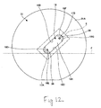
- FIGS. 7 to 14 are diagrams showing the manufacturing process of the light emitting device housing in accordance with the first embodiment of the invention.
- E denotes the region in which the light emitting device housing 11 is formed (which is hereinafter referred to as a "light emitting device housing formation region E")
- F denotes the ⁇ 110> plane of the silicon substrate 31 perpendicular to the ⁇ 100> plane of the silicon substrate 31.
- the silicon substrate 31 in which the top side 31A (fist main side) is a ⁇ 100> plane is prepared (silicon substrate preparation step).
- a resist film 33 having an opening 34 in a quadrangular shape in plan view is formed (resist film formation step).
- the opening 34 is formed in the resist film 33 corresponding to the light emitting device housing formation region E.
- the silicon substrate 31 is etched by wet etching using the resist film 33 having the opening 34 as a mask.
- This forms the concave part 18 including the side surfaces 18B and 18C which are the perpendicular surfaces made substantially perpendicular to the bottom surface 18A of the concave part 18, and the side surfaces 18D to 18G each configured to be an inclined surface reflecting light emitted from the light emitting device 12 toward above the light emitting device 12 (concave part formation step).
- the side surfaces 18B and 18C of the concave part 18 are the surfaces corresponding to the ⁇ 010> plane of the silicon substrate 31.
- the side surfaces 18D to 18G of the concave part 18 are the surfaces corresponding to the ⁇ 111> plane of the silicon substrate 31.
- the resist film 33 having the opening 34 is formed in a quadrangular shape, where the top side 31A is aligned to be a ⁇ 100> plane of the silicon substrate 31.
- the opening 34 is formed in such a way that a pair of opposing two sides 34A and 34B has an angle of 45 degrees with respect to the ⁇ 110> plane of the silicon substrate 31. Then, the silicon substrate 31 is etched by wet etching or anisotropic etching method with using the resist film 33 as a mask.
- this makes it possible to readily form the concave part 18 including the side surfaces 18B and 18C made substantially perpendicular to the bottom surface 18A, as well as the side surfaces 18D to 18G each configured to be an inclined surface to reflect the light emitted from the light emitting device 12 upwardly.
- the resist film 33 is removed.
- the through holes 17A and 17B are formed.
- a resist film (not shown) having openings corresponding to the positions at which the through holes 17A and 17B are formed is formed. With dry etching using the resist film as a mask, etching is carried out until the silicon substrate 31 is penetrated, thereby to form the through holes 17A and 17B.
- an insulation film 38 is formed on each portion of the silicon substrate 31 corresponding to the side surfaces of the through holes 17A and 17B.
- the via electrodes 15 and 16 are formed in the through holes 17A and 17B each having the insulation film 38 formed thereon, respectively.
- a structure corresponding to the light emitting device housing 11 is formed on a portion of the silicon substrate 31 corresponding to the light emitting device housing formation region E.
- the via electrodes 15 and 16 can be formed by, for example, a plating method. Whereas, as the material for the via electrodes 15 and 16, for example, Cu can be used.
- the portion of the silicon substrate 31 corresponding to the light emitting device housing formation region E is cut from the silicon substrate 31.
- the light emitting device housing 11 as shown in FIG. 14 is manufactured.
- the resist film 33 having the opening 34 in a tetragon in plan configuration is formed on the top side 31A of the silicon substrate 31 configured to be a ⁇ 100> plane.
- the opening 34 is formed such that any one pair of opposing two sides 34A and 34B of the two pairs of opposing two sides of the tetragon in plan configuration each form an angle of 45 degrees with the ⁇ 110> plane of the silicon substrate 31.
- the silicon substrate 31 is etched by wet etching using the resist film 33 as a mask.
- the concave part 18 including the side surfaces 18B and 18C made substantially perpendicular to the bottom surface 18A, and the side surfaces 18D to 18G each configured to be an inclined surface reflecting light from the light emitting device 12 toward above the light emitting device 12.
- FIG. 15 is a plan view of a light emitting apparatus in accordance with a second embodiment of the invention.
- the same constitutional elements as those of the light emitting apparatus 10 of the first embodiment are given the same reference numerals and signs.
- a light emitting apparatus 50 of the second embodiment has a light emitting device housing 51 and light emitting devices 53 and 54.
- the light emitting device housing 51 is configured similarly with the light emitting device housing 11, except that the through holes 17A and 17B, and the via electrodes 15 and 16 disposed on the light emitting device housing 11 of the first embodiment are disposed in the vicinity of the center of the bottom surface 18A of the concave part 18.
- the light emitting device 53 has a substantially square form in plan configuration, and is an element which emits light from all sides.
- the light emitting device 53 is provided on the bottom surface 18A of the concave part 18.
- the light emitting device 53 is arranged such that the side surface 53A of the light emitting device 53 faces the side surface 18Dof the concave part 18 configured to be an inclined surface, and such that the side surface 53B of the light emitting device 53 adjacent to the side surface 53A faces the side surface 18E of the concave part 18 configured to be an inclined surface.
- the light emitting device 53 has power supply terminals 56 and 57.
- the power supply terminal 56 is electrically connected with the via electrode 15 via a wire 58.
- the power supply terminal 57 is electrically connected with the via electrode 16 via a wire 59.
- the light emitting device 54 has a substantially square form in plan configuration, and is an element which emits light from all sides.
- the light emitting device 54 is provided on the bottom surface 18A of the concave part 18.
- the light emitting device 54 is arranged such that the side surface 54A of the light emitting device 54 faces the side surface 18F of the concave part 18 configured to be an inclined surface, and such that the side surface 54B of the light emitting device 54 adjacent to the side surface 54A of the light emitting device 54 faces the side surface 18G of the concave part 18 configured to be an inclined surface.
- the light emitting device 54 has power supply terminals 61 and 62.
- the power supply terminal 61 is electrically connected with the via electrode 15 by a wire 63.
- the power supply terminal 62 is electrically connected with the via electrode 16 by a wire 64. Having had this configurations, it is possible to avoid the emitted light from being shielded by the wires.
- the light emitting devices 53 and 54 are disposed on the bottom surface 18A of the concave part 18 such that the side surfaces 53A, 53B, 54A, and 54B of the light emitting devices 53 and 54 face any one of the side surfaces 18D to 18G of the concave part 18 each configured to be an inclined surface.
- the light emitting apparatus 50 it is possible to further improve the luminous efficiency of the light emitting apparatus 50 as compared with the light emitting apparatus 10 of the first embodiment.
- the light emitting apparatus 50 of the second embodiment with the foregoing configuration can provide the same effects as with the light emitting apparatus 10 of the first embodiment.
- the light emitting device housing 51 described in this embodiment can be manufactured with the same procedures as with the light emitting device housing 11 described in the first embodiment. Further, a description was given by taking, as an example, the case where the two light emitting devices 53 and 54 were mounted on the concave part 18 of the light emitting device housing 51. However, it is also acceptable that three or more light emitting devices are provided on the bottom surface 18A of the concave part 18.
- the "concave part” might also be denoted s a “recess part”.
- the present invention is applicable to a light emitting device housing for use in spotlight, headlight of a car, or the like, and a manufacturing method thereof, and a light emitting apparatus.
Landscapes
- Led Device Packages (AREA)
- Non-Portable Lighting Devices Or Systems Thereof (AREA)
Abstract
Description
- The present invention relates to a light emitting device housing and a manufacturing method thereof, and a light emitting apparatus. More specifically, it relates to a light emitting device housing including a concave part where a light emitting device is provided therein, manufacturing methods thereof, and a light emitting apparatus.
- FIG. 1 is a cross sectional view of a conventional light emitting apparatus. FIG. 2 is a plan view of the light emitting apparatus shown in FIG. 1.
- With reference to FIGS. 1 and 2, a conventional
light emitting apparatus 100 hasawiring substrate 101, alight emittingapparatus 102, and ametal frame 103. Thewiring substrate 101 has amain substrate 105, awiring 106, throughvias external connection terminals - The
main substrate 105 is shaped in a plate form, and has throughholes wiring 106 is provided on thetop side 105A of themain substrate 105. Thethrough via 107 is provided in thethrough hole 114A, and is connected to thewiring 106. Thethrough via 108 is provided in thethrough hole 114B. - The
external connection terminal 111 is provided on theback surface 105B of themain substrate 105. Theexternal connection terminal 111 is connected with the through via 107. Theexternal connection terminal 112 is provided on theback surface 105B of themain substrate 105. Theexternal connection terminal 112 is connected with the through via 108. - The
light emitting device 102 is provided on thewiring 106. Thelight emitting device 102 haspower supply terminals power supply terminal 117 is connected with thewiring 106, while thepower supply terminal 118 is electrically connected with the through via 108 by awire 119. - The
metal frame 103 is provided on thetop side 105A of themain substrate 105. Themetal frame 103 has aninner opening 121, and aninclined surface 122 forming the side surface of theinner opening 121. Theinner opening 121 is formed in a taper shape such as to increase in width from theback surface 103A side of themetal frame 103 toward thetop side 103B side thereof. Theinclined surface 122 is functioning as a reflector to reflect the light emitted from thelight emitting device 102 to a lens (not shown) which is disposed over thelight emitting apparatus 100. Provision of such aninclined surface 122 can improve the luminous efficiency of thelight emitting apparatus 100 such as known inJP-A-2004-281992 - However, although the conventional
light emitting apparatus 100 can be improved in luminous efficiency, it is hardly avoidable that the light emitted upwardly from thelight emitting apparatus 100 would eventually diffuse. In this regard, it is not an appropriate application to use the light emitted from thelight emitting apparatus 100 as a point light source. As for the light emitting apparatus serving as a point light source, they can be applied for a spotlight, a headlight of a vehicle, and so on. - In light of the above, the light emitting device housing according to independent claim 1, the light emitting apparatus according to claim 4, and he method for manufacturing a light emitting device housing according to independent claim 5 are provided.
- Further advantages, features, aspects and details of the invention are evident from the dependent claims, the description and the drawings.
- Under such circumstances, it is an object of the present invention to provide a light emitting device housing capable of improving the luminous efficiency, and capable of suppressing the diffusion of light emitted upwardly from the light emitting device, and a manufacturing method thereof, and a method for manufacturing a light emitting apparatus.
- In accordance with one of the aspects of the present invention, there is provided a light emitting device housing including a concave part where a light emitting device is provided therein, characterized in that the concave part has a plurality of side surfaces, at least one side surface among the plurality of the side surfaces is configured to be substantially perpendicular to the bottom surface of the concave part, and other side surfaces in said plurality of the side surfaces, in other words, other than those being configured as the perpendicular surface , are configured to be inclined surfaces to reflect the light from the light emitting device upwardly.
- In accordance with the invention, because of said at least one side surface that is substantially perpendicular to the bottom surface of the concave part, and the side surfaces having such inclined surfaces reflecting light from the light emitting device toward above the light emitting device, the present invention makes it possible to improve the luminous efficiency by suppressing the diffusion of light emitted upwardly from the light emitting device housing.
- In accordance with another aspect of the invention, there is provided a method for manufacturing a light emitting device housing including a concave part provided where a light emitting device is mounted therein, said methods comprising the steps of: a silicon substrate preparation step of preparing a silicon substrate of which principal surface is a <100> plane, a resist film formation step of forming a resist film on the principal surface of the silicon substrate, said resist film including an opening in a quadrangular shape in plan view, , and a concave part formation step of etching the silicon substrate to form the concave part by wet etching using the resist film as a mask, characterized in that forming the opening is performed in a way such that any one pair of the opposing two sides of the opening is aligned to have an angle of 45 degrees with respect to the <110> plane of the silicon substrate.
- In accordance with the invention, because of the resist film formed on the silicon substrate with a quadrangular shape opening of which one pair of the opposing two sides is aligned to have an angle of 45 degrees with respect to the <110> plane of the silicon substrate, it is possible to readily form the concave part which has the side surfaces of the concave part made substantially perpendicular to the bottom surface of the concave part, and the side surfaces of the concave part each configured to be an inclined surface so as to reflect the light emitted from the light emitting device upwardly.
- Embodiments are also directed to apparatuses for carrying out the disclosed methods and including apparatus parts for performing described method steps. Furthermore, embodiments are also directed to methods by which the described apparatus operates or by which the described apparatus is manufactured. It may include method steps for carrying out functions of the apparatus or manufacturing parts of the apparatus. The method steps may be performed by way of hardware components, firmware, a computer programmed by appropriate software, by any combination thereof or in any other manner.
- In accordance with the present invention, it is possible to improve the luminous efficiency of a light emitting apparatus, and it is possible to suppress the diffusion of light emitted upwardly from a light emitting device.
- The invention will be better understood by reference to the following description of embodiments of the invention taken in conjunction with the accompanying drawings, wherein:
- FIG. 1 shows a cross sectional view of a conventional light emitting apparatus;
- FIG. 2 shows a plan view of the light emitting apparatus shown in FIG. 1;
- FIG. 3 shows a plan view of a light emitting apparatus in accordance with a first embodiment of the invention;
- FIG. 4 shows a cross sectional view along line A-A of the light emitting apparatus shown in FIG. 3;
- FIG. 5 shows a cross sectional view along line B-B of the light emitting apparatus shown in FIG. 3;
- FIG. 6 shows a cross sectional view along line C-C of the light emitting apparatus shown in FIG. 3;
- FIG. 7 shows the first explanation view in a manufacturing step of a light emitting device housing in accordance with the first embodiment of the invention;
- FIG. 8 shows the second explanation view in a manufacturing step of the light emitting device housing in accordance with the first embodiment of the invention;
- FIG. 9 shows the third explanation view in a manufacturing step of the light emitting device housing in accordance with the first embodiment of the invention;
- FIG. 10 shows the fourth explanation view in a manufacturing step of the light emitting device housing in accordance with the first embodiment of the invention;
- FIG. 11 shows the fifth explanation view in a manufacturing step of the light emitting device housing in accordance with the first embodiment of the invention;
- FIG. 12 shows the sixth explanation view in a manufacturing step of the light emitting device housing in accordance with the first embodiment of the invention;
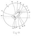
- FIG. 13 shows the seventh explanation view in a manufacturing step of the light emitting device housing in accordance with the first embodiment of the invention;
- FIG. 14 shows the eighth explanation view in a manufacturing step of the light emitting device housing in accordance with the first embodiment of the invention; and
- FIG. 15 shows a plan view of a light emitting apparatus in accordance with a second embodiment of the invention.
- Then, the invention will be described by way of embodiments with reference to the accompanying drawings.
- FIG. 3 is a plan view of a light emitting apparatus in accordance with a first embodiment of the invention. FIG. 4 is a cross sectional view along line A-A of the light emitting apparatus shown in FIG. 3.
- With reference to FIGS. 3 and 4, a
light emitting apparatus 10 of the first embodiment has a lightemitting device housing 11 and alight emitting device 12. - The light
emitting device housing 11 has a housingmain body 14 and viaelectrodes main body 14 is for housing thelight emitting device 12. As the material for the housingmain body 14, for example, silicon can be used. - The housing
main body 14 has throughholes concave part 18. - The through
holes main body 14. - The
concave part 18 is for housing thelight emitting device 12, and has sixside surfaces 18B to 18G (a plurality of side surfaces). - The
side surfaces concave part 18 are provided so as to face any one of two long sides of the four sides of thelight emitting device 12 which is a rectangle in plan configuration. - FIG. 5 is a cross sectional view along line B-B of the light emitting apparatus shown in FIG. 3. In FIG. 5, the same constitutional elements as those of the
light emitting apparatus 10 shown in FIG. 3 are given the same reference numerals and signs. - By reference to FIG. 5, the
side surface 18B of theconcave part 18 is configured to have a perpendicular surface substantially perpendicular to thebottom surface 18A of theconcave part 18. - The angle 01 formed between the
side surface 18B and thebottom surface 18A of theconcave part 18 is set to be substantially 90 degrees. Whereas, theside surface 18C of theconcave part 18 is configured to have a perpendicular surface substantially perpendicular to thebottom surface 18A of theconcave part 18. The angle formed between theside surface 18C and thebottom surface 18A of theconcave part 18 is set to be substantially 90 degrees. - Thus, the side surfaces 18B and 18C of the
concave part 18 for housing thelight emitting device 12 are configured to have perpendicular surfaces made substantially perpendicular to thebottom surface 18A of theconcave part 18. This can suppress the diffusion of light emitted from thelight emitting apparatus 10. As a result of this, it becomes possible to allow the light emitted from thelight emitting apparatus 10 to serve as a point source. - Further, the
light emitting device 12 is disposed such that each of the side surfaces 18B and 18C having the perpendicular surfaces is opposed to any one of two long sides of the four sides of thelight emitting device 12 which is a rectangle in plan configuration. This can improve the effect of suppressing the diffusion of light emitted upwardly from thelight emitting device 12. - When a silicon substrate is used as the base material for the housing
main body 14, the <010> planes of the silicon substrate can be utilized for the side surfaces 18B and 18C of theconcave part 18, which turns out significantly improving its manufacturing productivity. This is because a method of forming thehousing body 14 is directly performed on the silicon substrate, and etching the concave part of the housing body is performed by aligning one pair of the opposing two sides of the opening to have an angle of 45 degree with respect to the <110> plane of the silicon substrate as will be explained later on. - By reference to FIG. 3, the
side surface 18D of theconcave part 18 is disposed so as to be adjacent to the side surfaces 18B and 18E of theconcave part 18. Theside surface 18E of theconcave part 18 is disposed so as to be adjacent to the side surfaces 18C and 18D of theconcave part 18. In other words, the side surfaces 18D and 18E of theconcave part 18 are arranged so as to be adjacent to each other. - The
side surface 18F of theconcave part 18 is disposed so as to be adjacent to the side surfaces 18B and 18G of theconcave part 18. Theside surface 18G of theconcave part 18 is disposed so as to be adjacent to the side surfaces 18C and 18F of theconcave part 18. In other words, the side surfaces 18F and 18G of theconcave part 18 are arranged so as to be adjacent to each other. - FIG. 6 is a cross sectional view along line C-C of the light emitting apparatus shown in FIG. 3. In FIG. 6, the same constitutional elements as those of the
light emitting apparatus 10 shown in FIG. 3 are given the same reference numerals and signs. - By reference to FIG. 6, the
side surface 18D of theconcave part 18 is configured to have an inclined surface capable of reflecting light emitted from thelight emitting device 12 toward above thelight emitting device 12. Theangle 02 formed between theside surface 18D and thebottom surface 18A of theconcave part 18 can be set to be, for example, 54.7 degrees. The side surfaces 18E to 18G of theconcave part 18 are inclined surfaces shaped in the same form as that of theside surface 18D described above. - Thus, the side surfaces 18D to 18G of the
concave part 18 for housing thelight emitting device 12 are each configured to be an inclined surface capable of reflecting light from thelight emitting device 12 toward above thelight emitting device 12. This can improve the luminous efficiency of thelight emitting apparatus 10. - Further, the side surfaces 18D and 18E of the
concave part 18 configured to have incline surfaces are arranged so as to be adjacent to each other. As a result, it makes possible to reflect light with efficiency. This can further improve the luminous efficiency of thelight emitting apparatus 10. Whereas, the side surfaces 18F and 18G of theconcave part 18 configured to be incline surfaces are arranged so as to be adjacent to each other. This can further improve the luminous efficiency of thelight emitting apparatus 10. - When a silicon substrate is used as the base material for the housing
main body 14, the <111> plane of the silicon substrate can be utilized for the side surfaces 18D to 18G of theconcave part 18, which turns out significantly improving its manufacturing productivity. - This is because a method of forming the
housing body 14 is directly performed on the silicon substrate, and etching the concave part of the housing body is performed by aligning one pair of the opposing two sides of the opening to have an angle of 45 degree with respect to the <110> plane of the silicon substrate as will be explained later on. - With the light emitting device housing of this embodiment, the side surfaces 18B and 18C of the
concave part 18 for housing thelight emitting device 12 are each configured to have a perpendicular surface made substantially perpendicular to thebottom surface 18A of theconcave part 18. In addition, the side surfaces 18D to 18G of theconcave part 18 are each configured to be an inclined surface capable of reflecting light toward above thelight emitting device 12. As a result, it is possible to improve the luminous efficiency of thelight emitting apparatus 10, and it is possible to suppress the diffusion of light emitted from thelight emitting apparatus 10. - Then, by reference to FIGS. 3 and 4, the via
electrodes light emitting device 12 will be described in this order. The viaelectrode 15 is disposed in the throughhole 17A. The upper end portion of the viaelectrode 15 is electrically connected with apower supply terminal 22 of thelight emitting device 12 . The lower end portion of the viaelectrode 15 has a function as an external connection terminal. - The via
electrode 16 is disposed in the throughhole 17B. The upper end portion of the viaelectrode 16 is electrically connected with apower supply terminal 23 of thelight emitting device 12. The lower end portion of the viaelectrode 16 has a function as an external connection terminal. - As the material for the via
electrodes main body 14, an insulation film (not shown) is formed at the portion at which the throughholes main body 14 and the viaelectrodes - The
light emitting device 12 is mounted on thebottom surface 18A of theconcave part 18. Thelight emitting device 12 is an element which emits light from all sides. Thelight emitting device 12 is a rectangle in plan configuration, and haspower supply terminals power supply terminal 22 is electrically connected with the viaelectrode 15 via awire 25. Thepower supply terminal 23 is electrically connected with the viaelectrode 16 via awire 26. - With the light emitting apparatus of this embodiment, the side surfaces 18B and 18C of the
concave part 18 for housing thelight emitting device 12 are configured to have perpendicular surfaces made substantially perpendicular to thebottom surface 18A of theconcave part 18. In addition, the side surfaces 18D to 18G of theconcave part 18 are each configured to be an inclined surface capable of reflecting light toward above thelight emitting device 12. As a result, it is possible to improve the luminous efficiency of thelight emitting apparatus 10, and it is possible to suppress the diffusion of light emitted from thelight emitting apparatus 10. - In this embodiment, a description was given by taking the case where two perpendicular surfaces were provided. More specifically, the side surfaces 18B and 18C of the
concave part 18 are each configured to have a perpendicular surface as an example. However, it might be sufficient for achieving the object of the invention even if the perpendicular surface is formed on only one side surface of the side surfaces of theconcave part 18. Further, the respective numbers of the perpendicular surfaces and the inclines surfaces formed on the side surfaces of theconcave part 18 are not limited to those discussed in thelight emitting apparatus 10 of this embodiment. - FIGS. 7 to 14 are diagrams showing the manufacturing process of the light emitting device housing in accordance with the first embodiment of the invention. In FIGS. 7 to 14, as to the same structural elements of the light emitting
device housing 11 of the first embodiment, the same reference numerals and signs will be given. Whereas, in FIGS. 7 to 14, E denotes the region in which the light emittingdevice housing 11 is formed (which is hereinafter referred to as a "light emitting device housing formation region E"), and F denotes the <110> plane of thesilicon substrate 31 perpendicular to the <100> plane of thesilicon substrate 31. - First, in a step shown in FIG. 7, the
silicon substrate 31 in which thetop side 31A (fist main side) is a <100> plane is prepared (silicon substrate preparation step). - Then, in a step shown in FIG. 8, on the
top side 31A of thesilicon substrate 31, a resistfilm 33 having anopening 34 in a quadrangular shape in plan view is formed (resist film formation step). Theopening 34 is formed in the resistfilm 33 corresponding to the light emitting device housing formation region E. Theopening 34 is formed in such a way that any one pair of opposing two sides (e.g. 34A and 34B in Fig. 8) of the opening 34has an angle of 45 degrees (03 = 45 degrees) with respect to the <110> plane (F shown in FIG. 8) of thesilicon substrate 31. - Then, in a step shown in FIG. 9, the
silicon substrate 31 is etched by wet etching using the resistfilm 33 having the opening 34 as a mask. This forms theconcave part 18 including the side surfaces 18B and 18C which are the perpendicular surfaces made substantially perpendicular to thebottom surface 18A of theconcave part 18, and the side surfaces 18D to 18G each configured to be an inclined surface reflecting light emitted from thelight emitting device 12 toward above the light emitting device 12 (concave part formation step). The side surfaces 18B and 18C of theconcave part 18 are the surfaces corresponding to the <010> plane of thesilicon substrate 31. On the other hand, the side surfaces 18D to 18G of theconcave part 18 are the surfaces corresponding to the <111> plane of thesilicon substrate 31. - As explained above, the resist
film 33 having theopening 34 is formed in a quadrangular shape, where thetop side 31A is aligned to be a <100> plane of thesilicon substrate 31. In addition, theopening 34 is formed in such a way that a pair of opposing twosides silicon substrate 31. Then, thesilicon substrate 31 is etched by wet etching or anisotropic etching method with using the resistfilm 33 as a mask. As a result, this makes it possible to readily form theconcave part 18 including the side surfaces 18B and 18C made substantially perpendicular to thebottom surface 18A, as well as the side surfaces 18D to 18G each configured to be an inclined surface to reflect the light emitted from thelight emitting device 12 upwardly. - This can be realized by utilizing the physical characteristics of the semiconductor wafer, more specifically, the difference of the etching rates between the <010> plane and the <111> plane. That is, since the etching rate is much slower in <010> plane than in <111> plane, it is possible to keep the side surfaces 18B and 18C to be substantially perpendicular to the bottom surface or to the <100> surface due to the time required for revealing the inclined side surfaces 18D to 18G or for the <111> plane, which is relatively shorter than that of being required for revealing the <010> plane.
- Then, in a step shown in FIG. 10, the resist
film 33 is removed. Then, in a step shown in FIG. 11, in thesilicon substrate 31 corresponding to thebottom surface 18A of theconcave part 18, the throughholes holes silicon substrate 31 is penetrated, thereby to form the throughholes - Then, in a step shown in FIG. 12, on each portion of the
silicon substrate 31 corresponding to the side surfaces of the throughholes insulation film 38 is formed. - Then, in a step shown in FIG. 13, the via
electrodes holes insulation film 38 formed thereon, respectively. As a result of this, on a portion of thesilicon substrate 31 corresponding to the light emitting device housing formation region E, a structure corresponding to the light emittingdevice housing 11 is formed. - The via
electrodes electrodes - Subsequently, the portion of the
silicon substrate 31 corresponding to the light emitting device housing formation region E is cut from thesilicon substrate 31. As a result, the light emittingdevice housing 11 as shown in FIG. 14 is manufactured. - With the manufacturing method of the light emitting device housing of this embodiment, on the
top side 31A of thesilicon substrate 31 configured to be a <100> plane, the resistfilm 33 having the opening 34 in a tetragon in plan configuration is formed. In addition, theopening 34 is formed such that any one pair of opposing twosides silicon substrate 31. Then, thesilicon substrate 31 is etched by wet etching using the resistfilm 33 as a mask. As a result, it is possible to easily form theconcave part 18 including the side surfaces 18B and 18C made substantially perpendicular to thebottom surface 18A, and the side surfaces 18D to 18G each configured to be an inclined surface reflecting light from thelight emitting device 12 toward above thelight emitting device 12. - FIG. 15 is a plan view of a light emitting apparatus in accordance with a second embodiment of the invention. In FIG. 15, the same constitutional elements as those of the
light emitting apparatus 10 of the first embodiment are given the same reference numerals and signs. - With reference to FIG. 15, a
light emitting apparatus 50 of the second embodiment has a light emittingdevice housing 51 and light emittingdevices device housing 51 is configured similarly with the light emittingdevice housing 11, except that the throughholes electrodes device housing 11 of the first embodiment are disposed in the vicinity of the center of thebottom surface 18A of theconcave part 18. - The
light emitting device 53 has a substantially square form in plan configuration, and is an element which emits light from all sides. - The
light emitting device 53 is provided on thebottom surface 18A of theconcave part 18. Thelight emitting device 53 is arranged such that theside surface 53A of thelight emitting device 53 faces the side surface 18Dof theconcave part 18 configured to be an inclined surface, and such that theside surface 53B of thelight emitting device 53 adjacent to theside surface 53A faces theside surface 18E of theconcave part 18 configured to be an inclined surface. Thelight emitting device 53 haspower supply terminals power supply terminal 56 is electrically connected with the viaelectrode 15 via awire 58. Thepower supply terminal 57 is electrically connected with the viaelectrode 16 via awire 59. - The
light emitting device 54 has a substantially square form in plan configuration, and is an element which emits light from all sides. Thelight emitting device 54 is provided on thebottom surface 18A of theconcave part 18. Thelight emitting device 54 is arranged such that theside surface 54A of thelight emitting device 54 faces theside surface 18F of theconcave part 18 configured to be an inclined surface, and such that theside surface 54B of thelight emitting device 54 adjacent to theside surface 54A of thelight emitting device 54 faces theside surface 18G of theconcave part 18 configured to be an inclined surface. Thelight emitting device 54 haspower supply terminals power supply terminal 61 is electrically connected with the viaelectrode 15 by awire 63. - While, the
power supply terminal 62 is electrically connected with the viaelectrode 16 by awire 64. Having had this configurations, it is possible to avoid the emitted light from being shielded by the wires. - With the light emitting apparatus of this embodiment, the
light emitting devices bottom surface 18A of theconcave part 18 such that the side surfaces 53A, 53B, 54A, and 54B of thelight emitting devices concave part 18 each configured to be an inclined surface. As a result, it is possible to further improve the luminous efficiency of thelight emitting apparatus 50 as compared with thelight emitting apparatus 10 of the first embodiment. - Incidentally, the
light emitting apparatus 50 of the second embodiment with the foregoing configuration can provide the same effects as with thelight emitting apparatus 10 of the first embodiment. Whereas, the light emittingdevice housing 51 described in this embodiment can be manufactured with the same procedures as with the light emittingdevice housing 11 described in the first embodiment. Further, a description was given by taking, as an example, the case where the two light emittingdevices concave part 18 of the light emittingdevice housing 51. However, it is also acceptable that three or more light emitting devices are provided on thebottom surface 18A of theconcave part 18. - Generally, according to embodiments described herein, the "concave part" might also be denoted s a "recess part".
- Up to this point, the preferred embodiments of the invention were described in details. However, the invention is not limited to such specific embodiments, and various modifications / changes are possible within the scope of the gist of the invention described in the appended claims.
- The present invention is applicable to a light emitting device housing for use in spotlight, headlight of a car, or the like, and a manufacturing method thereof, and a light emitting apparatus.
Claims (5)
- Alight emitting device housing (11; 51)including a concave part where a light emitting device (12; 53; 54)is provided, comprising:the concave part (18) which has a plurality of side surfaces,at least one side surface among the plurality of the side surfaces is configured have a perpendicular surface (18B; 18C) so as to be substantially perpendicular to the bottom surface (18A) of the concave part, andinclined side surfaces, which are the side surfaces in said plurality of the side surfaces but other than said perpendicular surface, and configured to be inclined surfaces (18D-18G) to reflect light from the light emitting device upwardly.
- The light emitting device housing according to claim 1, wherein the inclined surfaces are arranged so as to be adjacent to each other.
- The light emitting device housing according to claim 1 or 2, wherein the light emitting device (12) has a rectangle or quadrangular shape, and the light emitting device is disposed such that at least one long side thereof faces the perpendicular surface of the light emitting device housing.
- A light emitting apparatus (10; 50) comprising:a light emitting device which is provided in a light emitting device housing (11; 51), according, to any of claims 1 to 3.
- A method for manufacturing a light emitting device housing (1; 51) including a concave part (18) where a light emitting device is mounted therein, said methods comprising the steps of:a silicon substrate preparation step of preparing a silicon substrate (31) of which principal surface is a <100> plane,a resist film formation step of forming a resist film (33) on the principal surface of the silicon substrate, said resist film including an opening in a quadrangular shape in plan view, anda concave part formation step of etching the silicon substrate to form the concave part (18) by wet etching using the resist film as a mask, whereinforming the opening is performed in a way such that any one pair of the opposing two sides of the opening is aligned to have an angle of 45 degrees with respect to the <110> plane of the silicon substrate.
Applications Claiming Priority (1)
| Application Number | Priority Date | Filing Date | Title |
|---|---|---|---|
| JP2006184860A JP2008016565A (en) | 2006-07-04 | 2006-07-04 | LIGHT EMITTING ELEMENT CONTAINER, MANUFACTURING METHOD THEREOF, AND LIGHT EMITTING DEVICE |
Publications (2)
| Publication Number | Publication Date |
|---|---|
| EP1876655A2 true EP1876655A2 (en) | 2008-01-09 |
| EP1876655A3 EP1876655A3 (en) | 2012-11-28 |
Family
ID=38544203
Family Applications (1)
| Application Number | Title | Priority Date | Filing Date |
|---|---|---|---|
| EP07013110A Withdrawn EP1876655A3 (en) | 2006-07-04 | 2007-07-04 | Light emitting device housing and a manufacturing method thereof, and light emitting apparatus using the same |
Country Status (4)
| Country | Link |
|---|---|
| US (1) | US7850344B2 (en) |
| EP (1) | EP1876655A3 (en) |
| JP (1) | JP2008016565A (en) |
| TW (1) | TW200805719A (en) |
Cited By (1)
| Publication number | Priority date | Publication date | Assignee | Title |
|---|---|---|---|---|
| EP2263268B1 (en) * | 2008-04-18 | 2016-01-06 | Tridonic Jennersdorf GmbH | Led module having a platform with a central recession |
Families Citing this family (7)
| Publication number | Priority date | Publication date | Assignee | Title |
|---|---|---|---|---|
| KR100820529B1 (en) | 2006-05-11 | 2008-04-08 | 엘지이노텍 주식회사 | Light emitting device and manufacturing method thereof, surface light emitting device |
| US20120068218A1 (en) * | 2010-09-17 | 2012-03-22 | Taiwan Semiconductor Manufacturing Company, Ltd. | Thermally efficient packaging for a photonic device |
| US20140367816A1 (en) * | 2013-06-12 | 2014-12-18 | Avago Technologies General Ip (Singapore) Pte.Ltd. | Photodetector device having light-collecting optical microstructure |
| JP6142883B2 (en) | 2015-02-05 | 2017-06-07 | 日亜化学工業株式会社 | Light emitting device |
| JP6444754B2 (en) | 2015-02-05 | 2018-12-26 | 日亜化学工業株式会社 | Light emitting device |
| JP6156402B2 (en) | 2015-02-13 | 2017-07-05 | 日亜化学工業株式会社 | Light emitting device |
| JP6874288B2 (en) | 2016-06-30 | 2021-05-19 | 日亜化学工業株式会社 | Light emitting device and backlight source |
Family Cites Families (15)
| Publication number | Priority date | Publication date | Assignee | Title |
|---|---|---|---|---|
| JPH0269382U (en) * | 1988-11-16 | 1990-05-25 | ||
| JPH075010A (en) * | 1993-02-25 | 1995-01-10 | Robert Bosch Gmbh | Mass flow sensor |
| DE10039433B4 (en) * | 2000-08-11 | 2017-10-26 | Osram Opto Semiconductors Gmbh | Semiconductor chip for optoelectronics |
| US6531328B1 (en) * | 2001-10-11 | 2003-03-11 | Solidlite Corporation | Packaging of light-emitting diode |
| JP4336137B2 (en) | 2003-01-24 | 2009-09-30 | 京セラ株式会社 | Light emitting element storage package and light emitting device |
| US7518155B2 (en) * | 2003-03-18 | 2009-04-14 | Sumitomo Electric Industries, Ltd. | Light emitting element mounting member, and semiconductor device using the same |
| JP3878579B2 (en) * | 2003-06-11 | 2007-02-07 | ローム株式会社 | Optical semiconductor device |
| JP4561954B2 (en) * | 2003-08-08 | 2010-10-13 | 東芝ライテック株式会社 | Light emitting device |
| JP2005260211A (en) * | 2004-02-10 | 2005-09-22 | Seiko Epson Corp | Light source device base, light source device base manufacturing method, light source device, and projector |
| JP4572312B2 (en) * | 2004-02-23 | 2010-11-04 | スタンレー電気株式会社 | LED and manufacturing method thereof |
| US7009285B2 (en) * | 2004-03-19 | 2006-03-07 | Lite-On Technology Corporation | Optoelectronic semiconductor component |
| TWI239670B (en) * | 2004-12-29 | 2005-09-11 | Ind Tech Res Inst | Package structure of light emitting diode and its manufacture method |
| JP2006245020A (en) * | 2005-02-28 | 2006-09-14 | Sharp Corp | Light emitting diode element and manufacturing method thereof |
| KR100665216B1 (en) * | 2005-07-04 | 2007-01-09 | 삼성전기주식회사 | Side-side light emitting diode with improved sidewall reflection structure |
| TWM318188U (en) * | 2007-02-02 | 2007-09-01 | Lighthouse Technology Co Ltd | Light-emitting diode |
-
2006
- 2006-07-04 JP JP2006184860A patent/JP2008016565A/en active Pending
-
2007
- 2007-07-03 US US11/773,155 patent/US7850344B2/en active Active
- 2007-07-04 EP EP07013110A patent/EP1876655A3/en not_active Withdrawn
- 2007-07-04 TW TW096124267A patent/TW200805719A/en unknown
Cited By (1)
| Publication number | Priority date | Publication date | Assignee | Title |
|---|---|---|---|---|
| EP2263268B1 (en) * | 2008-04-18 | 2016-01-06 | Tridonic Jennersdorf GmbH | Led module having a platform with a central recession |
Also Published As
| Publication number | Publication date |
|---|---|
| JP2008016565A (en) | 2008-01-24 |
| TW200805719A (en) | 2008-01-16 |
| US20080123344A1 (en) | 2008-05-29 |
| US7850344B2 (en) | 2010-12-14 |
| EP1876655A3 (en) | 2012-11-28 |
Similar Documents
| Publication | Publication Date | Title |
|---|---|---|
| US7850344B2 (en) | Light emitting device housing and a manufacturing method thereof, and light emitting apparatus using the same | |
| EP2672531B1 (en) | Light emitting device package and method of manufacturing the same | |
| US7183587B2 (en) | Solid metal block mounting substrates for semiconductor light emitting devices | |
| CN100505229C (en) | Semiconductor package and lead frame therefor | |
| US7247948B2 (en) | Semiconductor device and method for fabricating the semiconductor device | |
| TWI233189B (en) | Semiconductor device and manufacturing method thereof | |
| EP1267401A2 (en) | Semiconductor device and method of production of same | |
| US7824938B2 (en) | Method for manufacturing an LED chip package structure | |
| JP2009021426A (en) | Chip component type LED and manufacturing method thereof | |
| CN106409777A (en) | Packaged stacked semiconductor assembly with bottom element confined within dielectric cavity | |
| KR20130109319A (en) | Semiconductor light emitting device, light emitting module and lighting device | |
| US7180182B2 (en) | Semiconductor component | |
| KR20070069056A (en) | Semiconductor device and manufacturing method thereof | |
| TWI609511B (en) | Lead frame processing method and lead frame | |
| US20070278483A1 (en) | Light emitting device and method of manufacturing the same | |
| JP2001332769A (en) | Light-emitting diode lighting | |
| CN1534776A (en) | Semiconductor package and its lead frame | |
| CN101305453A (en) | Fine pitch interconnect and method of manufacture | |
| JP2016100552A (en) | Semiconductor device | |
| US20060104563A1 (en) | Optical semiconductor bare chip, printed wiring board, lighting unit and lighting device | |
| JP2000031545A (en) | Semiconductor light emitting device and method of manufacturing the same | |
| EP1696482A2 (en) | Semiconductor device package and method of manufacturing the same | |
| JPH11163416A (en) | Surface mount type photoelectric conversion device and method of manufacturing the same | |
| US9461438B2 (en) | Housing for laser diodes and method for producing a housing | |
| JP2015523718A (en) | SEMICONDUCTOR STRUCTURE AND METHOD FOR FORMING SEMICONDUCTOR STRUCTURE |
Legal Events
| Date | Code | Title | Description |
|---|---|---|---|
| PUAI | Public reference made under article 153(3) epc to a published international application that has entered the european phase |
Free format text: ORIGINAL CODE: 0009012 |
|
| AK | Designated contracting states |
Kind code of ref document: A2 Designated state(s): AT BE BG CH CY CZ DE DK EE ES FI FR GB GR HU IE IS IT LI LT LU LV MC MT NL PL PT RO SE SI SK TR |
|
| AX | Request for extension of the european patent |
Extension state: AL BA HR MK YU |
|
| PUAL | Search report despatched |
Free format text: ORIGINAL CODE: 0009013 |
|
| AK | Designated contracting states |
Kind code of ref document: A3 Designated state(s): AT BE BG CH CY CZ DE DK EE ES FI FR GB GR HU IE IS IT LI LT LU LV MC MT NL PL PT RO SE SI SK TR |
|
| AX | Request for extension of the european patent |
Extension state: AL BA HR MK RS |
|
| RIC1 | Information provided on ipc code assigned before grant |
Ipc: H01L 33/00 20100101AFI20121023BHEP |
|
| AKY | No designation fees paid | ||
| REG | Reference to a national code |
Ref country code: DE Ref legal event code: R108 |
|
| REG | Reference to a national code |
Ref country code: DE Ref legal event code: R108 Effective date: 20130731 |
|
| STAA | Information on the status of an ep patent application or granted ep patent |
Free format text: STATUS: THE APPLICATION IS DEEMED TO BE WITHDRAWN |
|
| 18D | Application deemed to be withdrawn |
Effective date: 20130529 |